humidity sensors using mems and standard …etd.lib.metu.edu.tr/upload/4/1124106/index.pdf ·...
TRANSCRIPT
HUMIDITY SENSORS USING MEMS AND STANDARD CMOS
TECHNOLOGIES
A THESIS SUBMITTED TO
THE GRADUATE SCHOOL OF NATURAL AND APPLIED SCIENCES
OF
THE MIDDLE EAST TECHNICAL UNIVERSITY
BY
BURAK OKCAN
IN PARTIAL FULFILLMENT OF THE REQUIREMENTS FOR THE DEGREE OF
MASTER OF SCIENCE
IN
THE DEPARTMENT OF ELECTRICAL AND ELECTRONICS ENGINEERING
AUGUST 2003
Approval of Graduate School of Natural and Applied Sciences.
_____________________________
Prof. Dr. Canan ÖZGEN
Director
I certify that this thesis satisfies all the requirements as a thesis for the degree of
Master of Science.
_____________________________
Prof. Dr. Mübeccel DEMİREKLER
Head of Department
This is to certify that we have read this thesis and that in our opinion it is fully
adequate, in scope and quality, as a thesis for the degree of Master of Science.
____________________________
Assoc. Prof. Dr. Tayfun AKIN
Supervisor
Examining Committee Members:
Assoc. Prof. Dr. Cengiz BEŞİKÇİ (Chairman)
____________________________
Assoc. Prof. Dr. Tayfun AKIN
____________________________
Assist. Prof. Dr. Özlem AYDIN ÇİVİ
____________________________
Dr. Deniz SABUNCUOĞLU TEZCAN
____________________________
Cem KURAL (M.S. in EE, ARÇELİK A.Ş.)
____________________________
iii
ABSTRACT
HUMIDITY SENSORS USING MEMS AND STANDARD CMOS
TECHNOLOGIES
Okcan, Burak
M. Sc., Department of Electrical and Electronics Engineering
Supervisor: Assoc. Prof. Dr. Tayfun Akın
August 2003, 127 pages
This thesis presents the development of humidity sensors using surface
micromachining and standard CMOS processes. Two types of humidity sensors are
designed and implemented. The first one is a capacitive humidity sensor with a
polyimide film as the humidity sensitive dielectric layer. The second sensor is a
thermal conductivity based humidity sensor, which measures the amount of humidity
using the difference between the thermal conductivity of the air and the water vapor.
The capacitive humidity sensor is fabricated by three mask process, where the
humidity sensitive polyimide layer is sandwiched between two metal electrodes. The
bottom electrode is designed in a heater resistor shape, which provides humidity
measurement at high relative humidity levels where there is the risk of water
condensation. Characterization results show that the fabricated sensor tracks the
humidity change with a sensitivity of 145fF/%RH, with nonlinearity less than 0.2%.
iv
The hysteresis of the sensor is 2.57% RH. The sensor is hybrid connected to a
switched capacitor readout circuit, which dissipates 1.75mW power. The measured
sensitivity of the hybrid module is 19.4mV/%RH with nonlinearity less than 0.2%.
Operation of the integrated heater is also verified by monitoring the resistance versus
temperature and resistance versus power characteristics.
The thermal conductivity based humidity sensor is implemented using
thermally isolated p-n junction diodes obtained by standard CMOS and post-CMOS
bulk silicon micromachining processes. Thermal isolation is achieved by anisotropic
bulk silicon etching using electrochemical etch stop technique in a TMAH solution.
One of the suspended diodes is sealed and has a fixed thermal conductance, while the
other one is exposed to the ambient and has humidity dependent thermal
conductance; therefore, they provide different diode voltages when they are heated
with same biasing currents. The difference between the diode voltages are converted
into current through a monolithic transconductance amplifier, and this current is
integrated by a switched capacitor integrator to obtain an amplified output signal.
The measured temperature sensitivity of the diodes is -1.3mV/K within 150ºC to
250ºC range at 100µA bias level. Relative humidity sensitivity of the sensor is
14.3mV/%RH, 26mV/%RH, and 46.9mV/%RH for 20ºC, 30ºC, and 40ºC ambient
temperature respectively with a nonlinearity less than 0.3%. The measured
hysteresis of the sensor is less than 1% at 20ºC and 30ºC ambient temperature
conditions. The sensor operates from a 5V supply and dissipates 1.38mW power.
v
ÖZ
MEMS VE STANDART CMOS TEKNOLOJİLERİ İLE NEM
SENSÖRLERİ
Okcan, Burak
Yüksek Lisans, Elektrik ve Elektronik Mühendisliği Bölümü
Tez Yöneticisi: Doç. Dr. Tayfun Akın
Ağustos 2003, 127 sayfa
Bu tezde MEMS ve standart CMOS süreci kullanılarak geliştirilmiş nem
sensörleri anlatılmaktadır. İki çeşit nem sensörü tasarlanmış ve üretilmiştir. Birinci
sensör, neme duyarlı dielektrik katmanı polyimide kullanılarak yapılmış kapasitif bir
sensördür. Diğer sensör, havanın ve su buharının ısıl iletkenlikleri arasındaki farkı
ölçen, ısıl iletkenlik bazlı nem sensörüdür.
Kapasitif sensör, polyimide katmanının iki metal elektrot arasına sıkıştırıldığı
üç maskelik bir süreçle üretilmiştir. Alt elektrot, su yoğunlaşması riskinin bulunduğu
yüksek nem seviyelerinde ölçüm yapma olanağı sağlayan ısıtıcı direnç şeklinde
tasarlanmıştır. Üretilen sensör üzerinde yapılan testler, sensörün nem değişimini
145fF/%RH’lik hassasiyet ve 0.2%’den düşük orantı katsayısı hatası ile algıladığını
göstermiştir. Sensör anahtarlamalı kapasitör okuma devresiyle entegre edilmiştir.
Hibrid yapının hassasiyeti 19.4mV/%RH, orantı katsayısı hatası 0.2%’den düşük
vi
olarak bulunmuştur. Sensörün histeresisi 2.57% RH’dir. Isıtıcının çalışması da
sıcaklığa ve güce bağlı direnç karakteristiğinin ölçümüyle doğrulanmıştır.
Isıl iletkenlik bazlı nem sensörü, standard CMOS ve CMOS sonrası gövde
aşındırma işlemleri kullanılarak elde edilen, ısıl olarak yalıtılmış diyotlar kullanılarak
elde edilmiştir. Isıl yalıtım, TMAH çözeltisi kullanılarak, yönlü silisyum gövde
aşındırması ve elektrokimyasal aşındırma-durdurma yöntemi ile sağlanmıştır.
Diyotlardan bir tanesi kapatılarak ısıl iletkenliği sabit tutulmuş, diğer diyot çevreyle
temas eder durumda bırakılarak ısıl iletkenliğinin nemle değişmesi sağlanmıştır. Bu
nedenle sabit akımla beslendiklerinde farklı çıkış gerilimleri üretmektedirler.
Diyotların çıkış gerilimleri arasındaki fark fark-geçiş-ileti yükselticisi ile akıma
dönüştürülmüş, akım da anahtarlamalı kapasitör entegratörü ile entegre edilerek
yükseltilmiş çıkış sinyali elde edilmiştir. 100µm akım seviyesinde ve 150ºC’den
250ºC’ye olan sıcaklık aralığında, diyotların sıcaklık hassasiyetleri -1.3mV/K olarak
ölçülmüştür. Sensörün bağıl nem hassasiyeti 20ºC, 30ºC ve 40ºC sıcaklık şartlarında
sırasıyla 14.3mV/%RH, 26mV/%RH ve 46.9mV/%RH olarak ölçülmüştür.
Sensörün ölçülen histeresisi 1% RH’den azdır. Sensör 5V ile beslenmektedir ve
1.38mW güç harcamaktadır.
vii
ACKNOWLEDGMENTS
I would like to express my appreciation and thanks to my supervisor Assoc.
Prof. Dr. Tayfun AKIN not only for his guidance and support during the
development of this thesis, but also for his friendly attitude towards me.
I would like to thank Orhan AKAR for the clean room training sessions, for
his great patience, and for his innovative ideas. I would also like to thank Dr. Deniz
S. TEZCAN and Yusuf TANRIKULU for their helps in the post processing of the
CMOS chips. I am also grateful to Dr. Selim EMİNOĞLU for sharing his circuit
design knowledge and experience with me. I would also like to thank METU-MET
staff for their help and guidance in the operation and maintenance of the sputtering
system. I am also thankful to my office mates Kağan TOPALLI, Mehmet Ünlü, Fırat
YAZICIOĞLU, Özge ZORLU, Hüseyin SAĞKOL, Murat TEPEGÖZ, M. Akif
ERİŞMİŞ, and Mustafa SANLI for creating a nice working atmosphere.
Finally, I would like to thank my family and all of my friends for their trust
and support through all my life.
viii
TABLE OF CONTENTS
ABSTRACT................................................................................................................iii
ÖZ…..………………………………………………………………………………...v
ACKNOWLEDGMENTS .........................................................................................vii
TABLE OF CONTENTS..........................................................................................viii
LIST OF TABLES ...................................................................................................... xi
LIST OF FIGURES ...................................................................................................xii
CHAPTER
1. INTRODUCTION ................................................................................................ 1
1.2.1 The Psychrometer.............................................................................. 6
1.2.2 The Dew-Point Hygrometer.............................................................. 7
1.2.3 Hygrometers Using Hygroscopic Materials...................................... 8
1.3.1 Resistive Humidity Sensors ............................................................ 11
1.3.2 Hygrometric Humidity Sensors ...................................................... 12
1.3.3 Gravimetric Humidity Sensors........................................................ 13
1.3.4 Optical Humidity Sensors ............................................................... 15
1.3.5 Thermal Humidity Sensors ............................................................. 15
1.3.6 Capacitive Humidity Sensors.......................................................... 17
2. A CAPACITIVE HUMIDITY SENSOR WITH AN INTEGRATED
HEATER ............................................................................................................. 25
1.1 Humidity Definition and Formulations......................................................... 3
1.2 Classical Humidity Measurement Methods .................................................. 6
1.3 Miniaturized Humidity Sensors .................................................................. 10
1.4 Research Objectives and Thesis Organization............................................ 22
ix
2.3.1 Thermal Simulations ....................................................................... 39
3. CAPACITIVE READOUT CIRCUIT ............................................................. 45
3.1.1 RC Oscillator................................................................................... 46
3.1.2 Capacitance to Current Converter................................................... 47
3.1.3 Switched Capacitor Charge Integrator ............................................ 48
3.2.1 Digital Section................................................................................. 54
3.2.2 Operational Amplifier ..................................................................... 55
3.2.3 Floor Plan and Layout..................................................................... 60
4. FABRICATION AND TEST RESULTS.......................................................... 63
4.2.1 The Humidity Response.................................................................. 67
4.2.2 Hysteresis Characteristics ............................................................... 70
4.2.3 Response Time Measurements........................................................ 72
4.2.4 Characterization Summary.............................................................. 72
5. A THERMAL CONDUCTIVITY BASED HUMIDITY SENSOR IN A
STANDARD CMOS PROCESS ....................................................................... 85
5.2.1 Temperature Sensitivity of Diodes ................................................. 89
5.2.2 Humidity Sensitive Diode Design................................................... 90
2.1 Polyimide as a Humidity Sensitive Material............................................... 25
2.2 Sensor Design ............................................................................................. 27
2.3 Integrated Heater Design............................................................................. 34
2.4 Device Fabrication ...................................................................................... 41
2.5 Conclusion .................................................................................................. 44
3.1 Capacitive Readout Techniques.................................................................. 45
3.2 Capacitive Readout Circuit Designed in This Study................................... 50
3.3 Conclusion .................................................................................................. 62
4.1 Fabrication Results...................................................................................... 63
4.2 Characterization Results.............................................................................. 66
4.3 Integrated Heater Tests ............................................................................... 75
4.4 The Hybrid Humidity Sensor Module ........................................................ 78
4.5 Conclusion .................................................................................................. 83
5.1 Humidity Sensing Principle ........................................................................ 85
5.2 Sensor Design ............................................................................................. 87
x
5.2.3 The Diode Layout ........................................................................... 95
5.5.1 Temperature Sensitivity Test ........................................................ 109
5.5.2 The Humidity Response................................................................ 110
5.5.3 Hysteresis Characteristics ............................................................. 111
6. CONCLUSIONS AND FUTURE WORK ..................................................... 114
REFERENCES......................................................................................................... 117
APPENDIX.............................................................................................................. 122
5.3 The Readout Circuit .................................................................................... 96
5.4 Post Processing ......................................................................................... 103
5.5 Fabrication and Test Results ..................................................................... 106
5.6 Conclusion ................................................................................................ 113
xi
LIST OF TABLES
TABLE
2.1: Design parameters of the two humidity sensors mask layouts. Pad frame and
dicing lines are not included in the total area calculation. Expected capacitance
values are calculated for 0.5 µm polyimide thickness. ...................................... 30
2.2: Expected resistance and the thermal conductance values of the heater electrodes.
The resistivity and the thermal conductivity of aluminum were taken as
2.665x10⁻⁸ Ω.m and 237 W/m.K respectively. .................................................. 36
2.3: Thickness, thermal conductivity, and electrical resistivity values of the
capacitive humidity sensor layers used in the thermal simulation..................... 39
2.4: Process flow for polyimide coating and patterning. .......................................... 42
3.1: Channel widths and lengths of the transistors used in the OTA. ....................... 57
3.2: Simulated figures of merit for the operational transconductance amplifier....... 60
4.1: Summary of the characterization results of the two capacitive humidity sensors
types. .................................................................................................................. 75
4.2: Comparison table for the performance parameters of the two humidity sensors.
............................................................................................................................ 83
5.1: Important design parameters of the humidity sensitive diode. .......................... 95
5.2: Important parameters of the TMAH etching and electrochemical etch stop
processes. ......................................................................................................... 106
5.3: Characterization summary of the thermal conductivity based humidity sensor.
.......................................................................................................................... 113
xii
LIST OF FIGURES
FIGURE
1.1: Saturation vapor pressure concept to explain the relative humidity: (a) vapor
pressure is less than saturation vapor pressure; (b) system is in equilibrium. ..... 4
1.2: Saturation water vapor pressure versus temperature graph [1]............................ 5
1.3: The schematic of a psychrometer [4]. .................................................................. 7
1.4: The structure of a dew-point hygrometer [1]. ...................................................... 8
1.5: A mechanical hygrometer, which uses the human hair as the hygroscopic
material [1]. .......................................................................................................... 9
1.6: The structure of a capacitive hygrometer [1]. .................................................... 10
1.7: A prototype of the dew point hygrometer [13]. ................................................. 12
1.8: The schematic diagram of the QCM humidity sensor [18]................................ 14
1.9: An SEM picture of the micro bridge heater humidity sensor [24]..................... 16
1.10: The cross sectional view of the thermal conductivity based humidity sensor
structure [25]. ..................................................................................................... 17
1.11: The cross sectional view of the capacitive humidity sensor with ceramic
humidity sensitive layer [27].............................................................................. 18
1.12: An SEM picture of the porous silicon capacitive humidity sensor [29]. ......... 19
1.13: The top view of the capacitive dew point detector [33]................................... 20
1.14: The capacitive humidity sensor with cylindrical polyimide columns integrated
with polysilicon heater [34]. .............................................................................. 21
1.15: The capacitive humidity sensor fabricated in a standard CMOS process [36].21
2.1: A symbolic view of the sensor structure. It is a variable capacitor with two
metal electrodes and a dielectric layer. .............................................................. 27
2.2: (a) Top views of both the top electrode and the polyimide layer, (b) cross
section of the structure. ...................................................................................... 29
xiii
2.3: The layout of the capacitive humidity sensor with 25µm metal line width. Total
layout dimensions are 1mm x 1mm. .................................................................. 31
2.4: The layout of the capacitive humidity sensor with 50µm metal line width. Total
layout dimensions are 1mm x 1mm. .................................................................. 32
2.5: The layout of the capacitive humidity sensor with 25µm metal width including
the pads and dicing lines. Total layout dimensions are 2400 µm x 1500 µm... 33
2.6: Three dimensional view of the bottom electrode designed in heater resistor
shape................................................................................................................... 34
2.7: The schematic of the lumped element thermal circuit representing the self
heating of the heater electrode. .......................................................................... 35
2.8: The layout of the heater with (a) 25µm, (b) 50µm metal width......................... 36
2.9: The layout of the capacitive humidity sensor with heater electrode including the
pad frame and dicing lines. Layout dimensions are 2400 x 1500 µm. ............. 37
2.10: The cross sectional view of the capacitive humidity sensor with the heater
electrode. ............................................................................................................ 38
2.11: CoventorWare windows that demonstrate the simulation results: (a) maximum
and minimum node temperature values, and (b) temperature distribution of the
sensor. Since the silicon base is very thick compared to the other layers, it is
not shown. Maximum temperature of the sensor reaches to 483 K at 100mW dc
power dissipation ............................................................................................... 40
2.12: Thickness versus spin speed graph for the polyimide film used as the dielectric
layer.................................................................................................................... 43
3.1: RC oscillator circuit structure. ........................................................................... 46
3.2: The circuit schematic of the capacitance to current converter........................... 48
3.3: The circuit schematic of the switched capacitor charge integrator. ................... 49
3.4: The block diagram of the readout circuit developed in this study. .................... 50
3.5: Switched capacitor charge integrator and the digital timing signals generated by
the digital section. .............................................................................................. 51
3.6: The circuit schematic of the switched capacitor integrator with offset
cancellation. ....................................................................................................... 53
3.7: The block diagram of the digital timing circuit. ................................................ 54
xiv
3.8: The circuit schematic of the folded cascode operational transconductance
amplifier. ............................................................................................................ 56
3.9: Simulated gain and phase characteristics of the operational transconductance
amplifier. ............................................................................................................ 58
3.10: The layout of the operational transconductance amplifier designed in 0.8µm
CMOS process. Transistors arrangement is done according to the stacked
layout technique. Total layout dimensions are 75µm x 90µm. ......................... 59
3.11: The layout of the switched capacitor readout circuit designed in a 0.8µm
CMOS process. Total layout dimensions are 640µm x 675µm. ....................... 61
4.1: SEM pictures of the fabricated capacitive humidity sensors with heater
electrodes with (a) 25µm metal line width, (b) 50µm metal line width. ........... 64
4.2: A zoomed view of the capacitive humidity sensor with the heater electrode.... 65
4.3: Initial capacitance measurements of the two capacitive humidity sensors with
(a) 25µm opening width, (b) 50µm opening width. Measurement frequency is 1
kHz. .................................................................................................................... 66
4.4: The capacitive humidity sensor wire bonded on a three pad alumina substrate.67
4.5: Capacitance versus relative humidity characteristics of the capacitive humidity
sensor performed at 20ºC ambient temperature. Sensitivity of the sensor is
145fF/%RH, with a nonlinearity of 0.13%. ....................................................... 68
4.6: The humidity response of the capacitive humidity sensor in the extended range
of operation at 20ºC ambient temperature. Nonlinearity increases above 70%
relative humidity. ............................................................................................... 69
4.7: The humidity response of the capacitive humidity sensor at different ambient
temperature levels. ............................................................................................. 70
4.8: Hysteresis test results of the capacitive humidity sensor. Calculated hysteresis
is 2.57% RH at 20ºC ambient temperature. ....................................................... 71
4.9: (a) The capacitance change monitored by the impedance analyzer during the
response time measurement; (b) impedance analyzer data converted to excel
graph................................................................................................................... 73
4.10: (a) The capacitance change monitored by the impedance analyzer during the
desorption time measurement; (b) impedance analyzer data converted to excel
graph. Desorption time is 12.1 seconds. ........................................................... 74
xv
4.11: Temperature versus resistance curve of the heater electrode........................... 75
4.12: Resistance versus power characteristics of the heater electrode...................... 76
4.13: Capacitance versus time graph monitored during the heating power applied on
the heater resistor. .............................................................................................. 77
4.14: Capacitance versus relative humidity plot when the sensor is heated by
applying 50mW power on the heater resistor at 20ºC ambient temperature. It is
seen that the linearity of the capacitance change increases between 70%RH and
90% RH range. ................................................................................................... 78
4.15: The hybrid humidity sensor module integrated on the TO package. ............... 79
4.16: Input signals and the output waveform of the integrator. ................................ 80
4.17: The output voltage response of the hybrid humidity sensor module. Sensitivity
is 19.4mV/%RH with a nonlinearity of 0.17%. ................................................. 81
4.18: Humidity sensor output versus temperature curves at different ambient relative
humidity values. ................................................................................................. 81
4.19: Hysteresis characteristics of the hybrid humidity sensor module. Calculated
hysteresis is 2.54% RH. ..................................................................................... 82
5.1: Thermal conductivity versus temperature plots for water vapor and air [59].... 86
5.2: A symbolic cross sectional view of the proposed sensor structure.................... 87
5.3: The lumped element thermal circuit representing the self heating of a diode
biased with constant current............................................................................... 88
5.4: Graphics showing the diode parameters with respect to the bias current and the
polysilicon length over width ratio: (a) operating temperature, (b) sensitivity. 93
5.5: Graphics showing the diode parameters with respect to the bias current at fixed
polysilicon dimensions: (a) sensitivity and operating temperature, (b) sensitivity
over power dissipation and operating temperature. ........................................... 94
5.6: The layout of the humidity sensitive diode designed in AMS 0.6µm CUP
process. Diode dimensions are 25µm x 25µm, where total layout dimensions
are 160µm x 160µm. .......................................................................................... 96
5.7: The block diagram of the readout circuit designed for the thermal conductivity
based humidity sensor chip. ............................................................................... 97
5.8: The circuit schematic of the transconductance amplifier................................... 98
xvi
5.9: The circuit schematic of the switched capacitor integrator with switching
configuration designed for offset cancellation................................................... 99
5.10: The layout of the humidity sensitive diode chip designed in the AMS 0.6µm
CMOS process. Total layout dimensions are 1650µm x 1900µm. ................. 101
5.11: A schematic view of the thermal conductivity based humidity sensor system.
……………………………………………………………………………………...102
5.12: The humidity sensitive diode chip placed on an alumina substrate............... 103
5.13: Four-electrode electrochemical etch stop configuration................................ 105
5.14: An SEM picture of the fabricated chip. ......................................................... 106
5.15: SEM pictures of the thermally isolated diode by post-CMOS anisotropic bulk
silicon etching. ................................................................................................. 107
5.16: The PCB used for the characterization of the thermal conductivity based
humidity sensor. ............................................................................................... 108
5.17: Output voltage versus temperature curves for the sensor and the reference
diodes at 100µA bias level. .............................................................................. 109
5.18: Output voltage versus relative humidity curve for the thermal conductivity
based humidity sensor. Humidity sensitivity is 14.3mV/%RH at 20ºC.......... 110
5.19: Output voltage versus relative humidity curves for different ambient
temperature conditions. .................................................................................... 111
5.20: Hysteresis test results of the humidity sensor at (a) 20ºC and (b) 30ºC ambient
temperatures. .................................................................................................... 112
1
1. CHAPTER 1
INTRODUCTION
Humidity, which is the amount of water vapor in the air, has an important role
in the quality of human life. In industry, optimum humidity conditions should be
provided on production lines for obtaining high quality products. For example, in
textile processing, generation of electrostatic charges during the fabrication may
cause the materials to cling. This is prevented by keeping the environment in damp
conditions. On the other hand, dry conditions are required in processing silicon
wafers in the clean room or assembling electrical products on the assembly line. In
agriculture, adequate environmental humidity conditions are needed to grow fruits
and vegetables. Similar conditions are needed in the preservation of products such as
food, cotton, and tobacco. Thus, the measurement and control of humidity have
significant importance in many areas for different purposes.
There have been continuous efforts for the measurement of humidity
throughout the development of science and engineering [1]. Several instruments for
measuring humidity based on different physical principles were invented in the 17th
century. Most important examples of these instruments are the hygroscopic
hygrometer, dew-point hygrometer, and psychrometer. These devices have large size
and slow response compared to modern instruments. However, their working
principles are still in use in the recent instruments.
CHAPTER 1
2
Today, thin film humidity sensors are widely used due to their small size, low
cost, low power consumption, and high performance. Various kinds of thin film
humidity sensors are available based on different measurement principles such as
resistive, capacitive, hygrometric, gravimetric, and thermal techniques. Thin film
humidity sensors still suffer from long term stability and chemical durability
problems in harsh environments. Instability at high relative humidity conditions due
to water condensation on the sensor surface is another drawback of most of the
commercial thin film humidity sensors.
This thesis reports two humidity sensors; one is based on the thin film
capacitive technique while the other one is based on the thermal technique. The
capacitive humidity sensor is integrated with a heater, which allows humidity
measurement at high relative humidity levels by reducing the relative humidity that
the sensor sees to a lower level. The fabricated sensor is hybrid connected to a
readout circuit for further signal processing of the sensor output. The second sensor
uses the difference between the thermal conductivity of air and water vapor. It is
fabricated by standard CMOS and post-CMOS processes, which allows the
integration of the sensor with the readout circuit monolithically. This sensor already
operates at high temperatures, which does not contain any risk of water condensation
at high relative humidity conditions.
This chapter presents the humidity concept and an overview of the humidity
sensors. Section 1.1 gives the definition of humidity and humidity related
formulations. This section also discusses the saturation vapor pressure and relative
humidity concepts, which are the fundamental terms used in humidity measurement.
Section 1.2 describes different principles of humidity measurement. Section 1.3
reviews the miniaturized humidity sensors and discusses their advantages and
disadvantages. Finally, section 1.4 gives the objectives and the organization of the
thesis.
3
1.1 Humidity Definition and Formulations
Humidity is the measure of the water vapor content of the atmosphere. It
forms a part of the total atmospheric pressure. The amount of atmospheric moisture
is proportional to the partial pressure of the water vapor, which allows a
measurement of the absolute humidity in the air. There are various ways of
expressing the moisture content of air, such as absolute humidity, specific humidity,
mixing ratio, and relative humidity. Absolute humidity is defined as the mass of
water vapor per unit volume of dry air [2]:
=mass of water vaporAbsolute humidity
volume of dry air (1.1)
Absolute humidity is expressed in g/m3, which is in fact the measure of the vapor
density of water.
Specific humidity and mixing ratio are two other ways of expressing the
amount of humidity in the air. Specific humidity is the ratio of the weight of water
vapor to the unit weight of air containing it [2]:
mass of water vaporSpecific humiditytotal mass of air
= (1.2)
On the other hand, the mixing ratio is the ratio of the mass of water vapor to a unit
mass of dry air containing it [2]:
mass of water vaporMixing ratiomass of dry air
= (1.3)
It is generally impractical to directly measure the quantities that are explained
above. There is a relatively simple experimental method of expressing the humidity,
which is relative humidity.
4
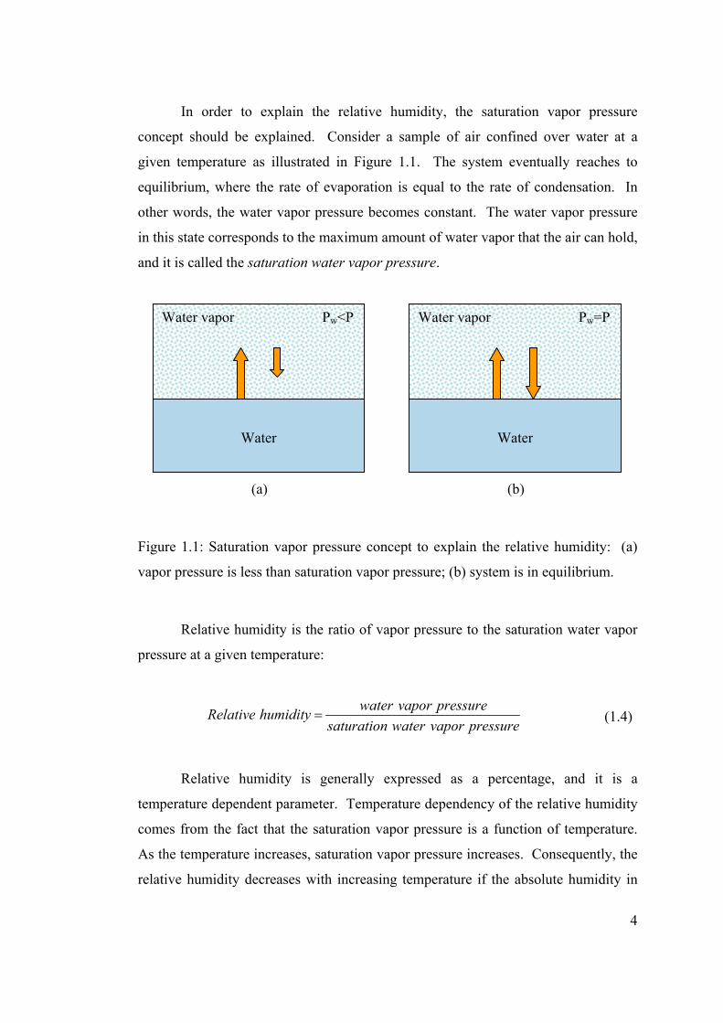
In order to explain the relative humidity, the saturation vapor pressure
concept should be explained. Consider a sample of air confined over water at a
given temperature as illustrated in Figure 1.1. The system eventually reaches to
equilibrium, where the rate of evaporation is equal to the rate of condensation. In
other words, the water vapor pressure becomes constant. The water vapor pressure
in this state corresponds to the maximum amount of water vapor that the air can hold,
and it is called the saturation water vapor pressure.
(a) (b)
Figure 1.1: Saturation vapor pressure concept to explain the relative humidity: (a)
vapor pressure is less than saturation vapor pressure; (b) system is in equilibrium.
Relative humidity is the ratio of vapor pressure to the saturation water vapor
pressure at a given temperature:
water vapor pressureRelative humiditysaturation water vapor pressure
= (1.4)
Relative humidity is generally expressed as a percentage, and it is a
temperature dependent parameter. Temperature dependency of the relative humidity
comes from the fact that the saturation vapor pressure is a function of temperature.
As the temperature increases, saturation vapor pressure increases. Consequently, the
relative humidity decreases with increasing temperature if the absolute humidity in
Water
Water vapor Pw<P
Water
Water vapor Pw=P
5
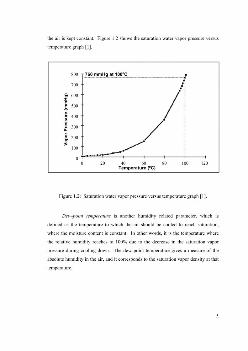
the air is kept constant. Figure 1.2 shows the saturation water vapor pressure versus
temperature graph [1].
760 mmHg at 100ºC 800
700
600
500
400
300
200
100
0 0 20 40 60 80 100 120
Temperature (ºC)
Vapo
r Pre
ssur
e (m
mH
g)
Figure 1.2: Saturation water vapor pressure versus temperature graph [1].
Dew-point temperature is another humidity related parameter, which is
defined as the temperature to which the air should be cooled to reach saturation,
where the moisture content is constant. In other words, it is the temperature where
the relative humidity reaches to 100% due to the decrease in the saturation vapor
pressure during cooling down. The dew point temperature gives a measure of the
absolute humidity in the air, and it corresponds to the saturation vapor density at that
temperature.
6
1.2 Classical Humidity Measurement Methods
There are various types of classical humidity measuring instruments, using
several different measurement methods such as psychrometers, dew-point
hygrometers, and hygrometers using hygroscopic materials [2]. All methods have
their own advantages and drawbacks, and a proper measurement method can be
selected depending on the application. Following subsections briefly explains these
methods. Then, Section 1.3 presents humidity sensors based on new
micromachining technologies.
1.2.1 The Psychrometer
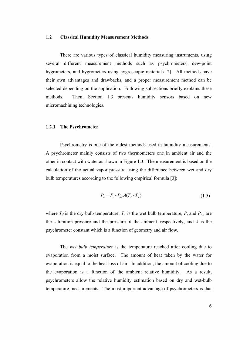
Psychrometry is one of the oldest methods used in humidity measurements.
A psychrometer mainly consists of two thermometers one in ambient air and the
other in contact with water as shown in Figure 1.3. The measurement is based on the
calculation of the actual vapor pressure using the difference between wet and dry
bulb temperatures according to the following empirical formula [3]:
- ( - )w s tot d wP P P A T T= (1.5)
where Td is the dry bulb temperature, Tw is the wet bulb temperature, Ps and Ptot are
the saturation pressure and the pressure of the ambient, respectively, and A is the
psychrometer constant which is a function of geometry and air flow.
The wet bulb temperature is the temperature reached after cooling due to
evaporation from a moist surface. The amount of heat taken by the water for
evaporation is equal to the heat loss of air. In addition, the amount of cooling due to
the evaporation is a function of the ambient relative humidity. As a result,
psychrometers allow the relative humidity estimation based on dry and wet-bulb
temperature measurements. The most important advantage of psychrometers is that
7
they do not require calibration. Main drawbacks are the requirement of the regular
replacement of distilled water and the requirement of air flow with a high flow rate.
Air flow in Dry bulb thermometer
Wet bulb thermometer
Air flow out
Side view Front view
Figure 1.3: The schematic of a psychrometer [4].
1.2.2 The Dew-Point Hygrometer
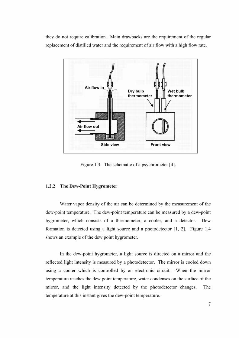
Water vapor density of the air can be determined by the measurement of the
dew-point temperature. The dew-point temperature can be measured by a dew-point
hygrometer, which consists of a thermometer, a cooler, and a detector. Dew
formation is detected using a light source and a photodetector [1, 2]. Figure 1.4
shows an example of the dew point hygrometer.
In the dew-point hygrometer, a light source is directed on a mirror and the
reflected light intensity is measured by a photodetector. The mirror is cooled down
using a cooler which is controlled by an electronic circuit. When the mirror
temperature reaches the dew point temperature, water condenses on the surface of the
mirror, and the light intensity detected by the photodetector changes. The
temperature at this instant gives the dew-point temperature.
8
This measurement method has a wide dynamic range, and it is very accurate.
Major disadvantages are the expensive setup, high power consumption, and difficult
maintenance of the system, such as the requirement of regular cleaning of the mirror
surface.
Air Inlet
Filter
Air Outlet
Processing Electronics
Cooler Base Thermometer
Light Source Photodetector
Figure 1.4: The structure of a dew-point hygrometer [1].
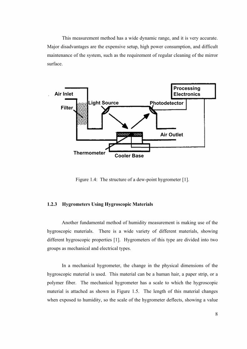
1.2.3 Hygrometers Using Hygroscopic Materials
Another fundamental method of humidity measurement is making use of the
hygroscopic materials. There is a wide variety of different materials, showing
different hygroscopic properties [1]. Hygrometers of this type are divided into two
groups as mechanical and electrical types.
In a mechanical hygrometer, the change in the physical dimensions of the
hygroscopic material is used. This material can be a human hair, a paper strip, or a
polymer fiber. The mechanical hygrometer has a scale to which the hygroscopic
material is attached as shown in Figure 1.5. The length of this material changes
when exposed to humidity, so the scale of the hygrometer deflects, showing a value
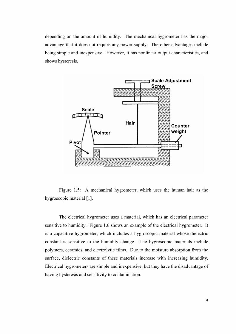
9
depending on the amount of humidity. The mechanical hygrometer has the major
advantage that it does not require any power supply. The other advantages include
being simple and inexpensive. However, it has nonlinear output characteristics, and
shows hysteresis.
Scale
Pointer
Hair Counter weight
Scale Adjustment Screw
Pivot
Figure 1.5: A mechanical hygrometer, which uses the human hair as the
hygroscopic material [1].
The electrical hygrometer uses a material, which has an electrical parameter
sensitive to humidity. Figure 1.6 shows an example of the electrical hygrometer. It
is a capacitive hygrometer, which includes a hygroscopic material whose dielectric
constant is sensitive to the humidity change. The hygroscopic materials include
polymers, ceramics, and electrolytic films. Due to the moisture absorption from the
surface, dielectric constants of these materials increase with increasing humidity.
Electrical hygrometers are simple and inexpensive, but they have the disadvantage of
having hysteresis and sensitivity to contamination.
10
Substrate
Upper Electrode
Hygroscopic Material
Lower Electrode
Figure 1.6: The structure of a capacitive hygrometer [1].
1.3 Miniaturized Humidity Sensors
Developments in the micromachining technology have encouraged the
development of miniaturized humidity sensors. Miniaturized humidity sensors have
the advantage of small size, low cost, low power consumption, and high performance
when compared to the classical measurement methods explained in the previous
section. Various types of miniaturized humidity sensors have been designed, which
use materials having different humidity dependent parameters. Major techniques of
measurement methods used in miniaturized humidity sensors can be listed as
resistive, capacitive, mechanical, gravimetric, and optical techniques. In addition to
these widely used techniques, there are some different techniques based on
electromagnetic and thermal humidity sensing methods. Miniaturized humidity
sensors have also been used in complex micro systems where they are integrated
with other types of transducers and electronic circuitries. Following subsections
shortly describe the humidity sensors based on micromachining techniques.
11
1.3.1 Resistive Humidity Sensors
Resistive humidity sensors are transducers that convert the humidity change
into resistance change. Ceramics, polymers and electrolytes are the main groups of
materials that have been used and reported for resistive humidity measurement.
These materials have humidity induced resistance characteristics, which allow the
humidity measurement by the measurement of resistance.
Various kinds of ceramics have been investigated as humidity sensitive
materials, such as TiO2, LiZnVO4, MnWO4, C2O, and Al2O3 [5-10]. In general,
ceramics have good chemical stability, high mechanical strength, and resistance to
high temperature. However, they have nonlinear humidity-resistance characteristics
and are not compatible with standard IC fabrication technologies.
Polymer based humidity sensors are another type of resistive humidity
sensors that are present in the literature. Some researchers have examined the
impedance changes of PVA (polyvinyl alcohol), TA (phthalocyaninosilicon), and
Nafion with relative humidity [11]. It has been reported that the humidity response
and the stability of the polymer films are dependent on different chemical properties
such as hydrophilicity, molecular, and ionic forms [11, 12]. Polymers also have
nonlinear humidity-resistance characteristics.
An example of the electrolyte based humidity sensors is the LiCl dew point
hygrometer fabricated with a composite of porous polymer and the salt [13]. The
humidity measurement is achieved by using the conductivity change of the LiCl-
polymer composition. The film is formed on an alumina substrate over interdigitated
platinum electrodes. The device is integrated with a heater and a temperature sensor,
which are connected to a control circuit to keep the vapor pressure of the saturated
LiCl solution equal to the vapor pressure of the atmosphere. The humidity
measurement is achieved by the measurement of the dew point temperature. Figure
1.7 presents a prototype of the dew point hygrometer.
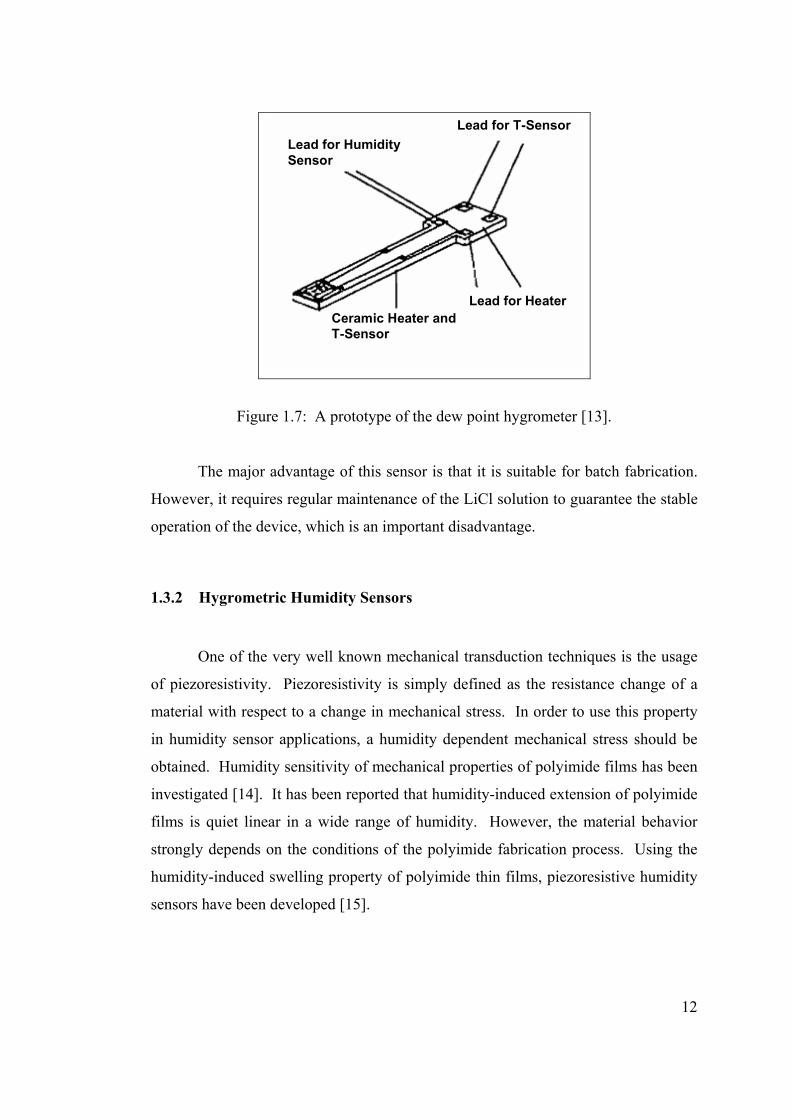
12
Lead for T-Sensor Lead for Humidity Sensor
Ceramic Heater and T-Sensor
Lead for Heater
Figure 1.7: A prototype of the dew point hygrometer [13].
The major advantage of this sensor is that it is suitable for batch fabrication.
However, it requires regular maintenance of the LiCl solution to guarantee the stable
operation of the device, which is an important disadvantage.
1.3.2 Hygrometric Humidity Sensors
One of the very well known mechanical transduction techniques is the usage
of piezoresistivity. Piezoresistivity is simply defined as the resistance change of a
material with respect to a change in mechanical stress. In order to use this property
in humidity sensor applications, a humidity dependent mechanical stress should be
obtained. Humidity sensitivity of mechanical properties of polyimide films has been
investigated [14]. It has been reported that humidity-induced extension of polyimide
films is quiet linear in a wide range of humidity. However, the material behavior
strongly depends on the conditions of the polyimide fabrication process. Using the
humidity-induced swelling property of polyimide thin films, piezoresistive humidity
sensors have been developed [15].
13
Another example of micro mechanical humidity transduction method is an
application of hygroscopic humidity sensing described in Section 1.2.3 into micro
technology. A mechanical-optoelectronic sensor unit has been developed using the
contraction-expansion property of black hair versus humidity [16]. Hair is attached
to a window, which determines the light intensity emitted from a LED to a
photodiode. This way, photocurrent of the photodiode changes with humidity. It has
been stated that the sensor response is less dependent on temperature because the
temperature expansion coefficient of hair is very small.
1.3.3 Gravimetric Humidity Sensors
Gravimetric humidity sensors are developed on the fact that the mass of a
hygroscopic material changes by humidity absorption. In this measurement method,
a resonator structure is fabricated with a hygroscopic material deposited on it.
Assuming that the absorbed water vapor behaves like a rigid mass, the change in
frequency is approximated with the equation of Sauerbrey [4]:
21-2 off m
A µρ∆ = ∆ (1.6)
where A is the surface area, f0 is the nominal frequency, µ is the shear modulus, ρ is
the density and ∆m is the change of mass caused by absorption.
Humidity absorptive properties of fullerene films have been investigated by
means of their effect on the resonance frequency of quartz resonators [17]. Test
results have shown that the resonance frequency of the resonators increase with the
increasing relative humidity of the environment. Resonators provide very high
sensitivity and low response time, but the frequency change with respect to relative
humidity demonstrates exponential characteristics.
14
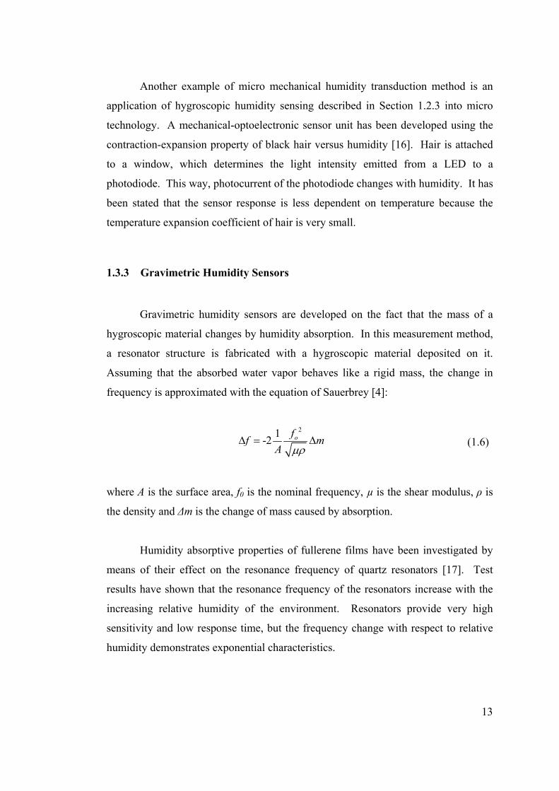
Another example of gravimetric humidity sensors is the Quartz Crystal
Microbalance (QCM) used as a humidity sensor [18]. Figure 1.8 shows the
schematic diagram of the QCM humidity sensor. In this method, water condensation
is produced by a Peltier element integrated with the QCM. A change of mass on the
crystal surface results in a decrease in the resonance frequency. Humidity
measurement is achieved by the measurement of the delay time between the
beginning of the Peltier supply and the beginning of the water condensation on the
quartz. The most important feature of this sensor is its relatively low response time.
Major disadvantages are the nonlinear characteristics and high temperature
dependence.
Quartz
Cold Side
Heat Sink
Hot Side
P PN N
TTL clock oscillator
Figure 1.8: The schematic diagram of the QCM humidity sensor [18].
There are other types of gravimetric humidity sensors such as the Surface
Acoustic Wave devices, where the phase velocity of surface waves change with the
absorption of water vapor [19, 20]. These devices also have nonlinear output
characteristics and require complicated systems for signal processing of sensor
outputs.
15
1.3.4 Optical Humidity Sensors
Optical methods have also been developed for humidity sensing applications.
The optical humidity measurements are based on the humidity dependence of the
amplitude, the polarization, and the frequency of an optical signal. Humidity
dependence of these parameters arises from the humidity induced dielectric constant
change of the medium where the signal propagation takes place.
An example of this type of humidity sensors is the optical fiber humidity
sensor fabricated using a hydrophilic gel (agarose) deposited on the thinner zone of a
biconically tapered single mode optical fiber [21]. The sensing mechanism relies on
the refractive index change of the agarose gel with respect to the relative humidity.
A variation of 6.5dB of the transmitted optical power has been obtained within the
30% to 80% relative humidity range. The sensor material shows a good
reproducibility and low hysteresis.
There are similar sensor structures present in the literature, which use the
refractive index change of the optical medium as a function of the absorbed water
vapor [22, 23]. These devices also show good reproducibility and low hysteresis
characteristics. However, they have quite nonlinear humidity response.
1.3.5 Thermal Humidity Sensors
Thermal humidity sensors have been developed by making use of the
difference in the thermal conductivity of air and that of water vapor. An absolute
humidity sensor has been demonstrated using a single micro air bridge heater [24].
The micro heater sensing region is heated up to a low temperature level at which the
thermal conductivity of the air and the water vapor is almost the same. Then, same
region is heated up to a temperature level where thermal conductivity difference
between the air and water vapor becomes significant. Heating is achieved by
applying double pulse currents. The resistance of the micro heater changes due to
16
the temperature coefficient of resistance (TCR) property. As a result, the difference
of the voltages in two cycles becomes a function of the absolute humidity in the air.
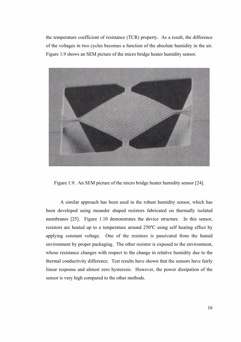
Figure 1.9 shows an SEM picture of the micro bridge heater humidity sensor.
Figure 1.9: An SEM picture of the micro bridge heater humidity sensor [24].
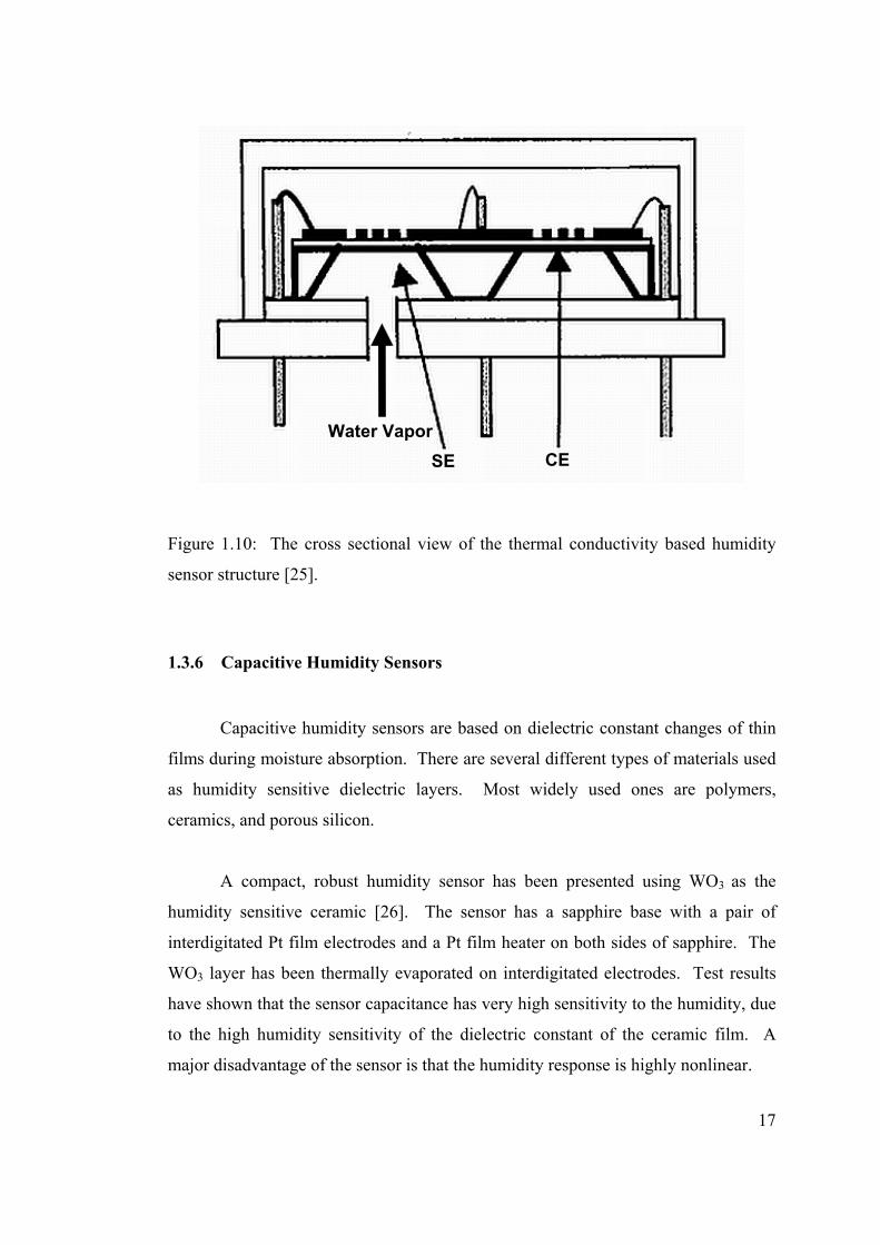
A similar approach has been used in the robust humidity sensor, which has
been developed using meander shaped resistors fabricated on thermally isolated
membranes [25]. Figure 1.10 demonstrates the device structure. In this sensor,
resistors are heated up to a temperature around 250ºC using self heating effect by
applying constant voltage. One of the resistors is passivated from the humid
environment by proper packaging. The other resistor is exposed to the environment,
whose resistance changes with respect to the change in relative humidity due to the
thermal conductivity difference. Test results have shown that the sensors have fairly
linear response and almost zero hysteresis. However, the power dissipation of the
sensor is very high compared to the other methods.
17
Water VaporCE SE
Figure 1.10: The cross sectional view of the thermal conductivity based humidity
sensor structure [25].
1.3.6 Capacitive Humidity Sensors
Capacitive humidity sensors are based on dielectric constant changes of thin
films during moisture absorption. There are several different types of materials used
as humidity sensitive dielectric layers. Most widely used ones are polymers,
ceramics, and porous silicon.
A compact, robust humidity sensor has been presented using WO3 as the
humidity sensitive ceramic [26]. The sensor has a sapphire base with a pair of
interdigitated Pt film electrodes and a Pt film heater on both sides of sapphire. The
WO3 layer has been thermally evaporated on interdigitated electrodes. Test results
have shown that the sensor capacitance has very high sensitivity to the humidity, due
to the high humidity sensitivity of the dielectric constant of the ceramic film. A
major disadvantage of the sensor is that the humidity response is highly nonlinear.
18
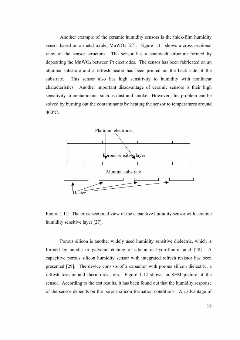
Another example of the ceramic humidity sensors is the thick-film humidity
sensor based on a metal oxide, MnWO4 [27]. Figure 1.11 shows a cross sectional
view of the sensor structure. The sensor has a sandwich structure formed by
depositing the MnWO4 between Pt electrodes. The sensor has been fabricated on an
alumina substrate and a refresh heater has been printed on the back side of the
substrate. This sensor also has high sensitivity to humidity with nonlinear
characteristics. Another important disadvantage of ceramic sensors is their high
sensitivity to contaminants such as dust and smoke. However, this problem can be
solved by burning out the contaminants by heating the sensor to temperatures around
400ºC.
Figure 1.11: The cross sectional view of the capacitive humidity sensor with ceramic
humidity sensitive layer [27].
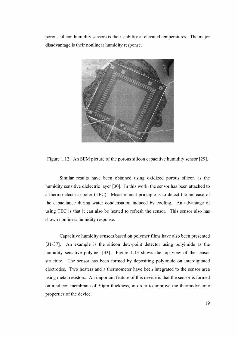
Porous silicon is another widely used humidity sensitive dielectric, which is
formed by anodic or galvanic etching of silicon in hydrofluoric acid [28]. A
capacitive porous silicon humidity sensor with integrated refresh resistor has been
presented [29]. The device consists of a capacitor with porous silicon dielectric, a
refresh resistor and thermo-resistors. Figure 1.12 shows an SEM picture of the
sensor. According to the test results, it has been found out that the humidity response
of the sensor depends on the porous silicon formation conditions. An advantage of
Porous sensitive layer
Alumina substrate
Platinum electrodes
Heater
19
porous silicon humidity sensors is their stability at elevated temperatures. The major
disadvantage is their nonlinear humidity response.
Figure 1.12: An SEM picture of the porous silicon capacitive humidity sensor [29].
Similar results have been obtained using oxidized porous silicon as the
humidity sensitive dielectric layer [30]. In this work, the sensor has been attached to
a thermo electric cooler (TEC). Measurement principle is to detect the increase of
the capacitance during water condensation induced by cooling. An advantage of
using TEC is that it can also be heated to refresh the sensor. This sensor also has
shown nonlinear humidity response.
Capacitive humidity sensors based on polymer films have also been presented
[31-37]. An example is the silicon dew-point detector using polyimide as the
humidity sensitive polymer [33]. Figure 1.13 shows the top view of the sensor
structure. The sensor has been formed by depositing polyimide on interdigitated
electrodes. Two heaters and a thermometer have been integrated to the sensor area
using metal resistors. An important feature of this device is that the sensor is formed
on a silicon membrane of 50µm thickness, in order to improve the thermodynamic
properties of the device.
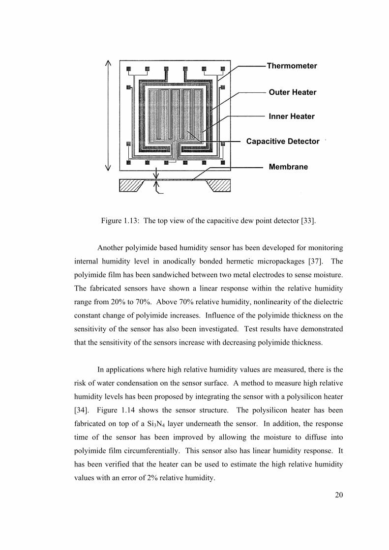
20
Thermometer
Outer Heater
Inner Heater
Capacitive Detector
Membrane
Figure 1.13: The top view of the capacitive dew point detector [33].
Another polyimide based humidity sensor has been developed for monitoring
internal humidity level in anodically bonded hermetic micropackages [37]. The
polyimide film has been sandwiched between two metal electrodes to sense moisture.
The fabricated sensors have shown a linear response within the relative humidity
range from 20% to 70%. Above 70% relative humidity, nonlinearity of the dielectric
constant change of polyimide increases. Influence of the polyimide thickness on the
sensitivity of the sensor has also been investigated. Test results have demonstrated
that the sensitivity of the sensors increase with decreasing polyimide thickness.
In applications where high relative humidity values are measured, there is the
risk of water condensation on the sensor surface. A method to measure high relative
humidity levels has been proposed by integrating the sensor with a polysilicon heater
[34]. Figure 1.14 shows the sensor structure. The polysilicon heater has been
fabricated on top of a Si3N4 layer underneath the sensor. In addition, the response
time of the sensor has been improved by allowing the moisture to diffuse into
polyimide film circumferentially. This sensor also has linear humidity response. It
has been verified that the heater can be used to estimate the high relative humidity
values with an error of 2% relative humidity.
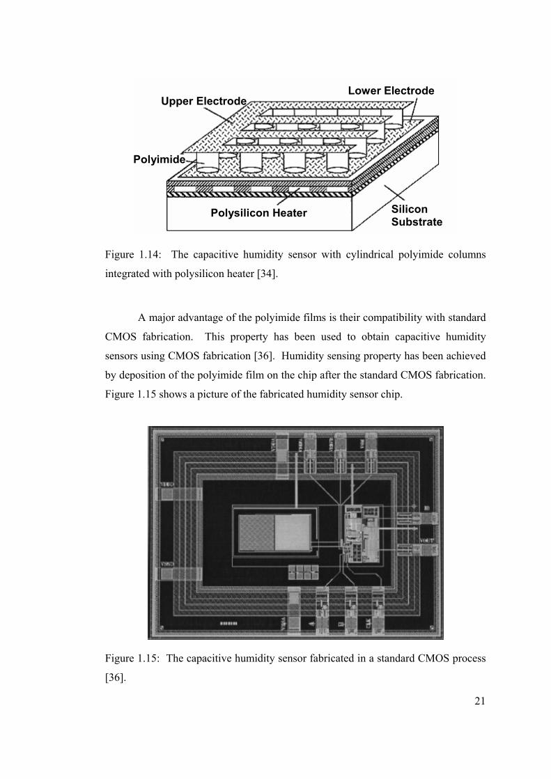
21
Polysilicon Heater Silicon Substrate
Lower Electrode Upper Electrode
Polyimide
Figure 1.14: The capacitive humidity sensor with cylindrical polyimide columns
integrated with polysilicon heater [34].
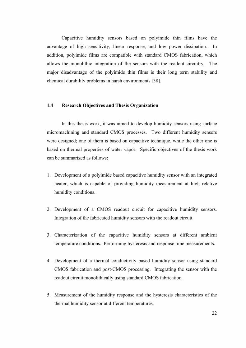
A major advantage of the polyimide films is their compatibility with standard
CMOS fabrication. This property has been used to obtain capacitive humidity
sensors using CMOS fabrication [36]. Humidity sensing property has been achieved
by deposition of the polyimide film on the chip after the standard CMOS fabrication.
Figure 1.15 shows a picture of the fabricated humidity sensor chip.
Figure 1.15: The capacitive humidity sensor fabricated in a standard CMOS process
[36].
22
Capacitive humidity sensors based on polyimide thin films have the
advantage of high sensitivity, linear response, and low power dissipation. In
addition, polyimide films are compatible with standard CMOS fabrication, which
allows the monolithic integration of the sensors with the readout circuitry. The
major disadvantage of the polyimide thin films is their long term stability and
chemical durability problems in harsh environments [38].
1.4 Research Objectives and Thesis Organization
In this thesis work, it was aimed to develop humidity sensors using surface
micromachining and standard CMOS processes. Two different humidity sensors
were designed; one of them is based on capacitive technique, while the other one is
based on thermal properties of water vapor. Specific objectives of the thesis work
can be summarized as follows:
1. Development of a polyimide based capacitive humidity sensor with an integrated
heater, which is capable of providing humidity measurement at high relative
humidity conditions.
2. Development of a CMOS readout circuit for capacitive humidity sensors.
Integration of the fabricated humidity sensors with the readout circuit.
3. Characterization of the capacitive humidity sensors at different ambient
temperature conditions. Performing hysteresis and response time measurements.
4. Development of a thermal conductivity based humidity sensor using standard
CMOS fabrication and post-CMOS processing. Integrating the sensor with the
readout circuit monolithically using standard CMOS fabrication.
5. Measurement of the humidity response and the hysteresis characteristics of the
thermal humidity sensor at different temperatures.
23
The research started with a literature search on the humidity sensors that have
been developed using various different measurement techniques. After the decision
on the method to be focused on in this study, masks of the sensor layers were
designed. Fabrication of the capacitive sensors was processed in the clean room
facilities of METU. Readout circuit for the capacitive humidity sensor was designed
and fabricated in AMS 0.8µm CMOS process. Thermal conductivity based humidity
sensor was designed and fabricated in AMS 0.6µm CMOS process. Characterization
tests of the sensors were performed in testing laboratories of METU. Rest of the
thesis is organized as follows:
Chapter 2 describes the design of the capacitive humidity sensor and the
integrated heater. This chapter discusses the important geometrical parameters that
affect the sensor performance. The theory of self heating is also explained and the
thermal simulations of the integrated heater are presented. Finally, mask layouts of
the sensors are given.
Chapter 3 presents the CMOS readout circuit developed for capacitive
humidity sensors. This chapter includes a summary of the capacitive readout
techniques that have been presented in the literature. Design of the analog and
digital blocks of the readout circuit are explained, and the chip layout is given.
Chapter 4 presents the characterization results of the capacitive humidity
sensors. Humidity response of the capacitive sensors is demonstrated with the
hysteresis test results and the response time measurements. Characterization results
of the integrated heater are also presented, and the effect of heating on the sensor
response is investigated. This chapter also presents the characterization results of the
hybrid humidity sensor module, which is obtained by connecting the capacitive
sensor with the readout circuit.
Chapter 5 describes the design of a thermal conductivity based humidity
sensor developed in a standard CMOS process. This chapter discusses the effect of
structural parameters on the sensor performance and presents the layout of the

24
sensor. In addition, design of the readout circuit is explained, and the post
processing of the chip is discussed. This chapter also includes the characterization
results of the thermal conductivity based humidity sensor.
Finally, Chapter 6 presents the conclusions of the thesis and gives suggestions
for future studies.
25
2. CHAPTER 2
A CAPACITIVE HUMIDITY SENSOR WITH
AN INTEGRATED HEATER
This chapter presents the design and implementation of a capacitive type
humidity sensor with an integrated heater. Section 2.1 discusses polyimide films and
their important characteristics for humidity sensing applications. These
characteristics include some figures of merit such as sensitivity, long term stability,
chemical durability and also processing methods in microfabrication. Sections 2.2
and 2.3 describe the capacitive sensor and integrated heater structures, respectively.
These sections also include some theoretical calculations and simulation results
regarding the performances of the sensor and the heater. Following sections present
the fabrication and test results of both the sensor and the heater. Finally, test results
are discussed, and further improvements are proposed.
2.1 Polyimide as a Humidity Sensitive Material
Polyimide films are developed for electronic industries to be used as
interlayer dielectrics, passivation layers, and stress buffers. They also have
applications in the field of integrated circuit fabrication as inter-metal dielectrics,
sacrificial layers, and surface planarizers [38].
There are several reasons that make polyimide films have applications in
microelectronics industry. The polyimide is chemically inert in its cured form, and
CHAPTER 2
26
thermally stable material up to temperatures around 450 °C. In addition, it is a
perfect planarizer used to planarize irregular surfaces. It also has a low relative
permittivity and high breakdown voltage, which makes it desirable for high speed
applications. However, it has some important disadvantages for the integrated circuit
fabrication. Most important disadvantage is its high humidity sensitivity, which
results in humidity dependency of the output response of circuits. Although this
property is unwanted in microelectronic circuits, it makes polyimide films very
attractive for humidity sensing applications. Being thermally stable and fully
compatible with silicon processing technology, polyimide is the most widely used
humidity sensitive dielectric in capacitive humidity sensors.
Humidity responses of polyimide films have been investigated in many works
[31-35]. Experiments show that the dielectric constant of polyimide films change
from about 3 to 4 as the relative humidity changes from 0%RH to 100%RH.
Moreover, the dielectric constant change with respect to the humidity change is
almost linear especially within the 20%RH to 70%RH range. Polyimide deposition
can be performed at the end of a CMOS fabrication process, and therefore humidity
sensors, which are monolithically integrated with the readout circuit, can be obtained
[36]. Major drawbacks of polyimide films can be stated as long term stability and
chemical durability problems [38]. In harsh environments, humidity responses of
polyimide films may drift in time. In addition, the presence of water for a long time
may cause the failure of the device.
Polyimide films can be divided into two groups according to the method that
they are processed in microfabrication. Photosensitive polyimide films are processed
like photoresists. They are masked, exposed to UV light, and patterned by their own
developers. Non-photosensitive polyimide films are patterned by dry or wet etching
like a regular layer in microelectronics, so an additional photolithography step is
required in the fabrication. On the other hand, using photosensitive polyimide films
considerably reduces the number of processing steps and makes the process easier.
Furthermore, since they are directly masked and developed, the resulting pattern has
better defined features.
27
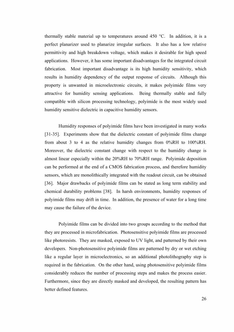
2.2 Sensor Design
In this study, a capacitive humidity sensor with a sandwich structure was
designed. The sensor is simply a capacitor with two metal electrodes and a
polyimide layer as the humidity sensitive dielectric. Figure 2.1 shows a symbolic
view of the sensor structure.
Figure 2.1: A symbolic view of the sensor structure. It is a variable capacitor with
two metal electrodes and a dielectric layer.
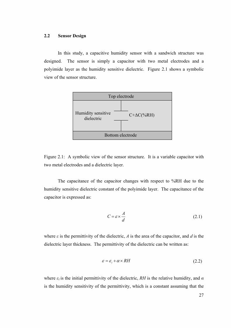
The capacitance of the capacitor changes with respect to %RH due to the
humidity sensitive dielectric constant of the polyimide layer. The capacitance of the
capacitor is expressed as:
ACd
ε= × (2.1)
where ε is the permittivity of the dielectric, A is the area of the capacitor, and d is the
dielectric layer thickness. The permittivity of the dielectric can be written as:
i RHε ε α= + × (2.2)
where εi is the initial permittivity of the dielectric, RH is the relative humidity, and α
is the humidity sensitivity of the permittivity, which is a constant assuming that the
C+∆C(%RH) Humidity sensitive dielectric
Top electrode
Bottom electrode
28
humidity sensitivity is linear. If Equation 2.2 is inserted into Equation 2.1, the
capacitance is written as:
iA AC RHd d
ε α= × + × × (2.3)
In the sandwich structure, the area of the capacitor is equal to the area of the
metal electrodes. In microfabrication, there is no limitation on the surface area of a
deposited metal, so very high capacitance values can be achieved using the sandwich
structure. This is the major advantage of the sandwich shaped capacitors over the
interdigitated electrode capacitors where the capacitor area is dependent on the
electrode thickness, which is limited by the process. High capacitance values make it
easier to convert the capacitance change into voltage change using electronic circuits,
since the effect of parasitic capacitances becomes less important.
The most important parameter of a capacitive humidity sensor is its
sensitivity. In capacitive humidity sensors, the sensitivity of a device is generally
expressed in capacitance per %RH form. From Equation 2.3, sensitivity of the
sensor is found as:
ASd
α= × (2.4)
The sensitivity is directly related with the humidity sensitivity of the polyimide film
and the geometry of the sensor. It should be noted that the sensitivity increases with
increasing initial sensor capacitance. The sensitivity of a sensor can also be
increased by increasing the amount of moisture absorbed by the polyimide layer [37].
In order to increase the amount of absorbed moisture, the top electrode of the sensor
is designed in a meshed structure. This way, a wider access path is provided for the
moisture into the polyimide film, so the sensitivity of the sensor is improved. Figure
2.2(a) shows the structure of the top electrode.
29
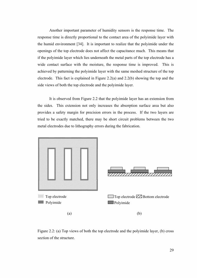
Another important parameter of humidity sensors is the response time. The
response time is directly proportional to the contact area of the polyimide layer with
the humid environment [34]. It is important to realize that the polyimide under the
openings of the top electrode does not affect the capacitance much. This means that
if the polyimide layer which lies underneath the metal parts of the top electrode has a
wide contact surface with the moisture, the response time is improved. This is
achieved by patterning the polyimide layer with the same meshed structure of the top
electrode. This fact is explained in Figure 2.2(a) and 2.2(b) showing the top and the
side views of both the top electrode and the polyimide layer.
It is observed from Figure 2.2 that the polyimide layer has an extension from
the sides. This extension not only increases the absorption surface area but also
provides a safety margin for precision errors in the process. If the two layers are
tried to be exactly matched, there may be short circuit problems between the two
metal electrodes due to lithography errors during the fabrication.
(a) (b)
Figure 2.2: (a) Top views of both the top electrode and the polyimide layer, (b) cross
section of the structure.
Top electrode Polyimide
Top electrode Polyimide
Bottom electrode
30
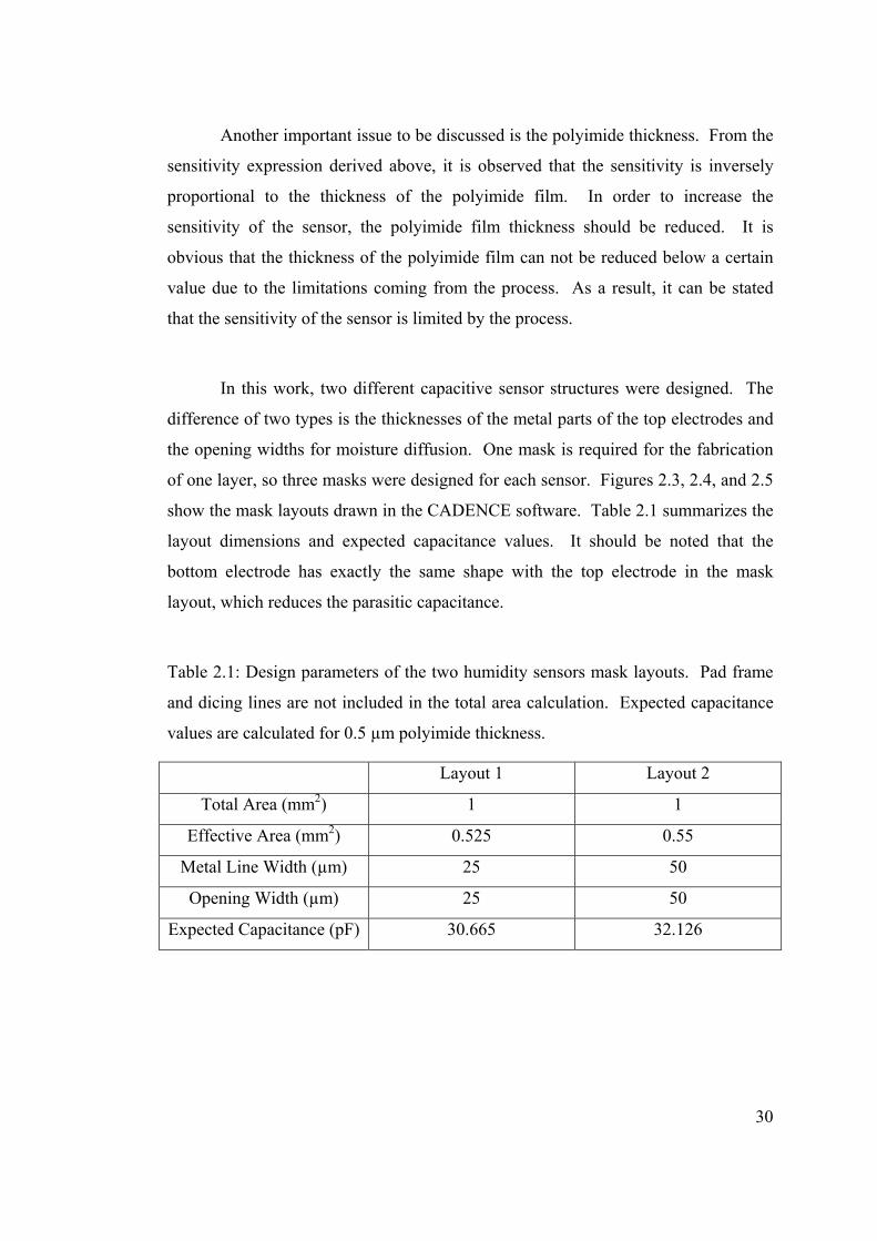
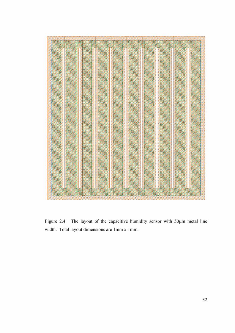
Another important issue to be discussed is the polyimide thickness. From the
sensitivity expression derived above, it is observed that the sensitivity is inversely
proportional to the thickness of the polyimide film. In order to increase the
sensitivity of the sensor, the polyimide film thickness should be reduced. It is
obvious that the thickness of the polyimide film can not be reduced below a certain
value due to the limitations coming from the process. As a result, it can be stated
that the sensitivity of the sensor is limited by the process.
In this work, two different capacitive sensor structures were designed. The
difference of two types is the thicknesses of the metal parts of the top electrodes and
the opening widths for moisture diffusion. One mask is required for the fabrication
of one layer, so three masks were designed for each sensor. Figures 2.3, 2.4, and 2.5
show the mask layouts drawn in the CADENCE software. Table 2.1 summarizes the
layout dimensions and expected capacitance values. It should be noted that the
bottom electrode has exactly the same shape with the top electrode in the mask
layout, which reduces the parasitic capacitance.
Table 2.1: Design parameters of the two humidity sensors mask layouts. Pad frame
and dicing lines are not included in the total area calculation. Expected capacitance
values are calculated for 0.5 µm polyimide thickness.
Layout 1 Layout 2
Total Area (mm2) 1 1
Effective Area (mm2) 0.525 0.55
Metal Line Width (µm) 25 50
Opening Width (µm) 25 50
Expected Capacitance (pF) 30.665 32.126
31
Figure 2.3: The layout of the capacitive humidity sensor with 25µm metal line
width. Total layout dimensions are 1mm x 1mm.
32
Figure 2.4: The layout of the capacitive humidity sensor with 50µm metal line
width. Total layout dimensions are 1mm x 1mm.
33
Figure 2.5: The layout of the capacitive humidity sensor with 25µm metal width
including the pads and dicing lines. Total layout dimensions are 2400 µm x 1500
µm.
34
2.3 Integrated Heater Design
In some humidity sensing applications, implementation of a heater with a
humidity sensor is necessary as discussed in Chapter 1. In general, the heater is
implemented around or underneath the sensor with a resistor structure or a discrete
heating element is attached to the sensor. These methods require extra fabrication
steps or complex packaging, which increase the cost of the device.
The capacitive humidity sensor developed in this study is integrated with a
heater using a different approach than the reported ones in literature. Bottom
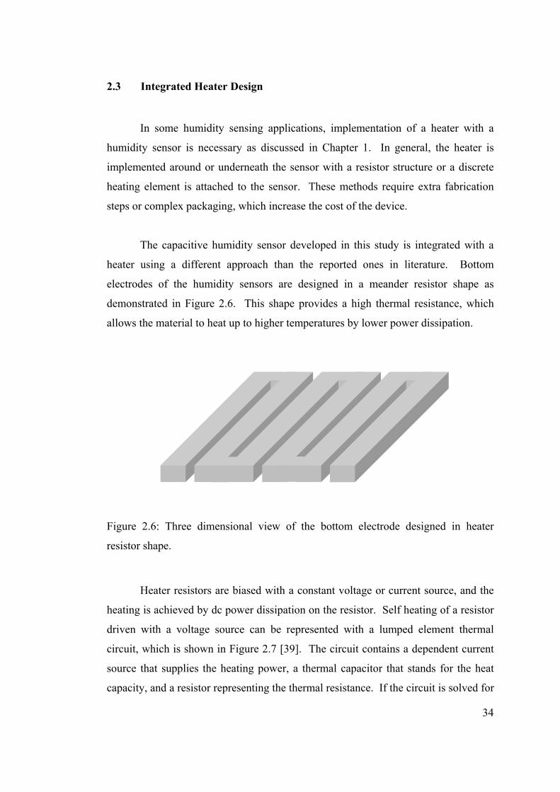
electrodes of the humidity sensors are designed in a meander resistor shape as
demonstrated in Figure 2.6. This shape provides a high thermal resistance, which
allows the material to heat up to higher temperatures by lower power dissipation.
Figure 2.6: Three dimensional view of the bottom electrode designed in heater
resistor shape.
Heater resistors are biased with a constant voltage or current source, and the
heating is achieved by dc power dissipation on the resistor. Self heating of a resistor
driven with a voltage source can be represented with a lumped element thermal
circuit, which is shown in Figure 2.7 [39]. The circuit contains a dependent current
source that supplies the heating power, a thermal capacitor that stands for the heat
capacity, and a resistor representing the thermal resistance. If the circuit is solved for
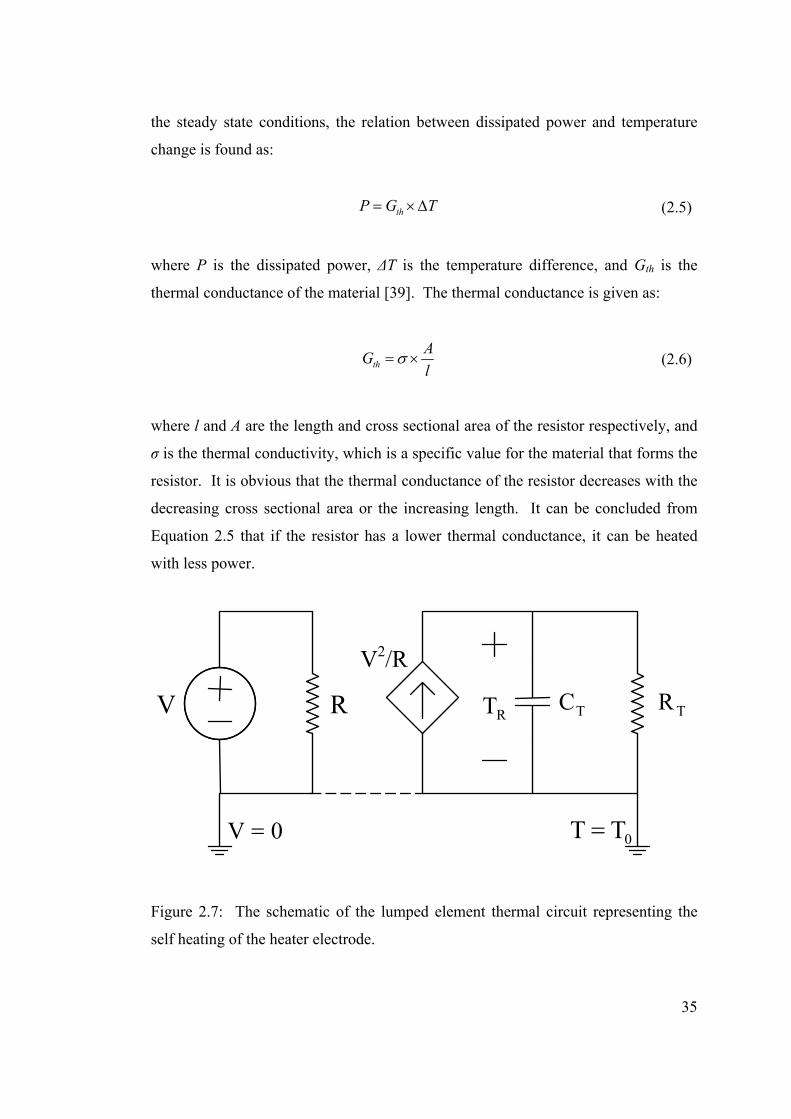
35
the steady state conditions, the relation between dissipated power and temperature
change is found as:
thP G T= ×∆ (2.5)
where P is the dissipated power, ∆T is the temperature difference, and Gth is the
thermal conductance of the material [39]. The thermal conductance is given as:
thAGl
σ= × (2.6)
where l and A are the length and cross sectional area of the resistor respectively, and
σ is the thermal conductivity, which is a specific value for the material that forms the
resistor. It is obvious that the thermal conductance of the resistor decreases with the
decreasing cross sectional area or the increasing length. It can be concluded from
Equation 2.5 that if the resistor has a lower thermal conductance, it can be heated
with less power.
Figure 2.7: The schematic of the lumped element thermal circuit representing the
self heating of the heater electrode.
RV TRTC
0V = 0TT =
RT
V2/R
36
Two different mask layouts were designed for the heater electrodes of the two
sensor structures demonstrated in the previous section. It should be noted that the
masks for the polyimide layer and the top electrode are exactly same as the
previously demonstrated layouts. Only the mask for the heater electrode was
modified according to the heater resistor shape. Figures 2.8 and 2.9 show the mask
layouts for the heater electrodes and the layout including the pad frame and dicing
lines respectively. Table 2.2 summarizes the expected resistance and the thermal
conductance values of the two heater structures assuming that the heaters are 0.5µm
thick aluminum.
Table 2.2: Expected resistance and the thermal conductance values of the heater
electrodes. The resistivity and the thermal conductivity of aluminum were taken as
2.665x10⁻⁸ Ω.m and 237 W/m.K respectively.
Layout 1 Layout2
Resistance (Ω) 43 11
Thermal Conductance (W/K) 1.46x10⁻⁷ 5.72x10⁻⁷
(a) (b)
Figure 2.8: The layout of the heater with (a) 25µm, (b) 50µm metal width.
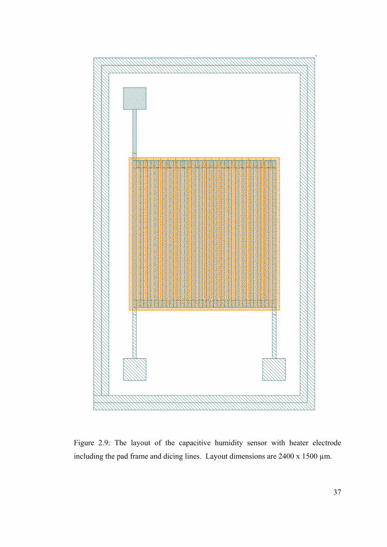
37
Figure 2.9: The layout of the capacitive humidity sensor with heater electrode
including the pad frame and dicing lines. Layout dimensions are 2400 x 1500 µm.
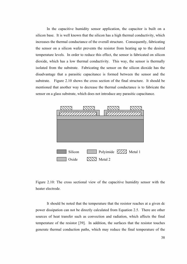
38
In the capacitive humidity sensor application, the capacitor is built on a
silicon base. It is well known that the silicon has a high thermal conductivity, which
increases the thermal conductance of the overall structure. Consequently, fabricating
the sensor on a silicon wafer prevents the resistor from heating up to the desired
temperature levels. In order to reduce this effect, the sensor is fabricated on silicon
dioxide, which has a low thermal conductivity. This way, the sensor is thermally
isolated from the substrate. Fabricating the sensor on the silicon dioxide has the
disadvantage that a parasitic capacitance is formed between the sensor and the
substrate. Figure 2.10 shows the cross section of the final structure. It should be
mentioned that another way to decrease the thermal conductance is to fabricate the
sensor on a glass substrate, which does not introduce any parasitic capacitance.
Figure 2.10: The cross sectional view of the capacitive humidity sensor with the
heater electrode.
It should be noted that the temperature that the resistor reaches at a given dc
power dissipation can not be directly calculated from Equation 2.5. There are other
sources of heat transfer such as convection and radiation, which affects the final
temperature of the resistor [39]. In addition, the surfaces that the resistor touches
generate thermal conduction paths, which may reduce the final temperature of the
Silicon
Oxide
Metal 1 Polyimide
Metal 2
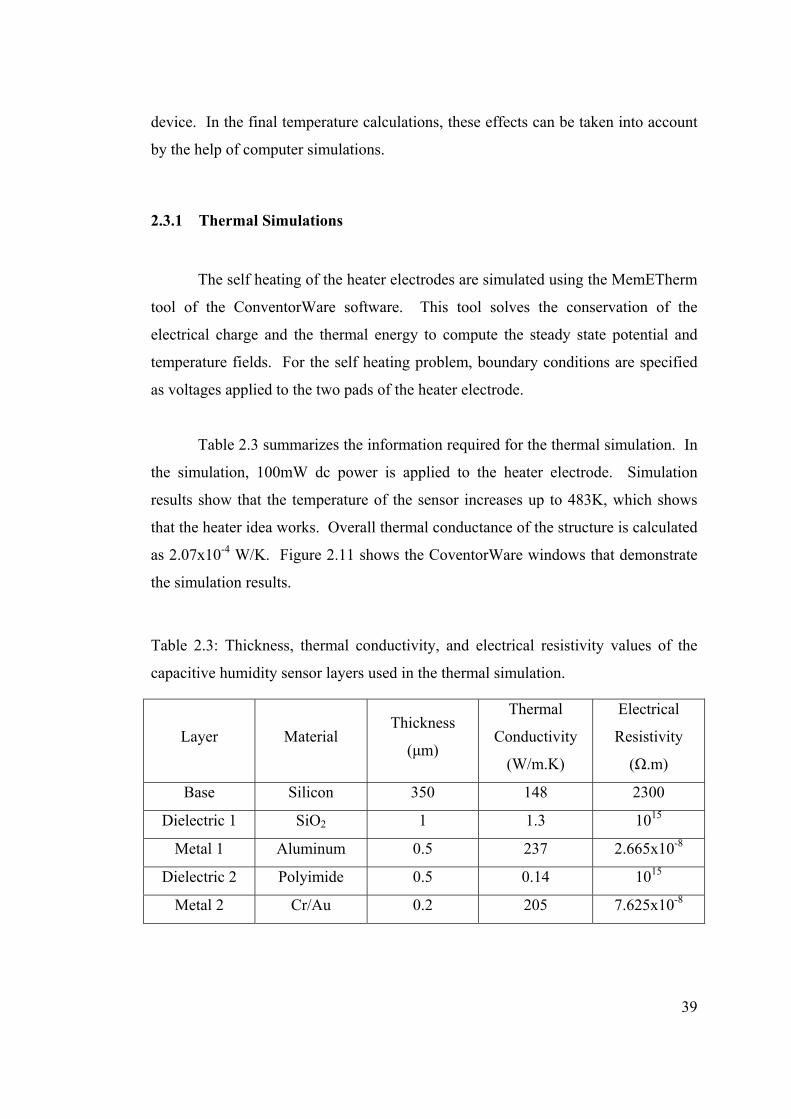
39
device. In the final temperature calculations, these effects can be taken into account
by the help of computer simulations.
2.3.1 Thermal Simulations
The self heating of the heater electrodes are simulated using the MemETherm
tool of the ConventorWare software. This tool solves the conservation of the
electrical charge and the thermal energy to compute the steady state potential and
temperature fields. For the self heating problem, boundary conditions are specified
as voltages applied to the two pads of the heater electrode.
Table 2.3 summarizes the information required for the thermal simulation. In
the simulation, 100mW dc power is applied to the heater electrode. Simulation
results show that the temperature of the sensor increases up to 483K, which shows
that the heater idea works. Overall thermal conductance of the structure is calculated
as 2.07x10⁻⁴ W/K. Figure 2.11 shows the CoventorWare windows that demonstrate
the simulation results.
Table 2.3: Thickness, thermal conductivity, and electrical resistivity values of the
capacitive humidity sensor layers used in the thermal simulation.
Layer Material Thickness
(µm)
Thermal
Conductivity
(W/m.K)
Electrical
Resistivity
(Ω.m)
Base Silicon 350 148 2300
Dielectric 1 SiO2 1 1.3 1015
Metal 1 Aluminum 0.5 237 2.665x10⁻⁸
Dielectric 2 Polyimide 0.5 0.14 1015
Metal 2 Cr/Au 0.2 205 7.625x10⁻⁸
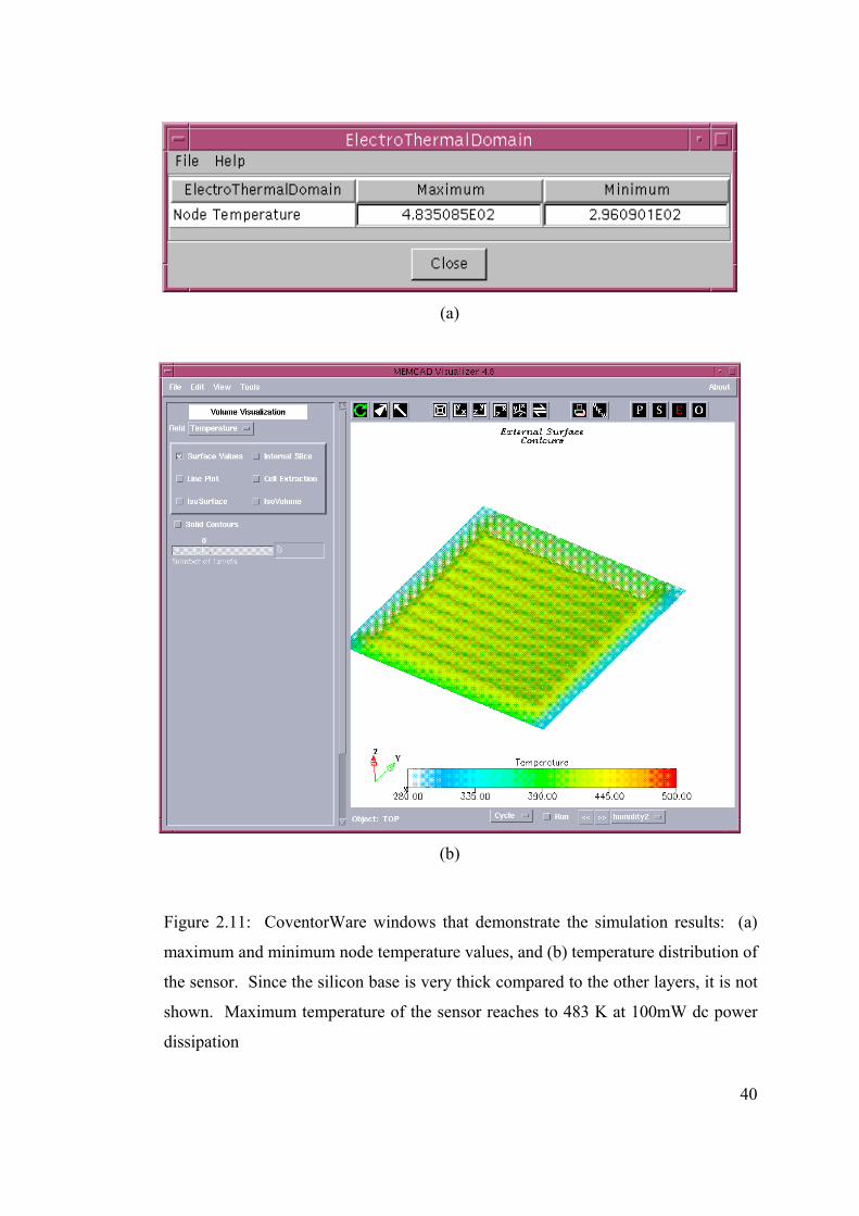
40
(a)
(b)
Figure 2.11: CoventorWare windows that demonstrate the simulation results: (a)
maximum and minimum node temperature values, and (b) temperature distribution of
the sensor. Since the silicon base is very thick compared to the other layers, it is not
shown. Maximum temperature of the sensor reaches to 483 K at 100mW dc power
dissipation
41
2.4 Device Fabrication
Fabrication of the capacitive humidity sensors has three main steps. These
are two metallization and one polyimide deposition steps, which require lithography
and patterning operations.
The first metallization is performed by the sputter deposition technique. In
the sputter deposition, a target material which is to be deposited is bombarded by
argon ions. This is achieved by keeping the target material at a negative potential
and creating positively charged argon ions by the help of an electric field. The target
material is sputtered away by momentum transfer, and ejected surface atoms are
deposited on the substrate placed on the anode.
In the fabrication of the bottom electrode, Al is sputtered on SiO2 coated three
inch wafers at 2kW power for 20 minutes using a magnetron sputtering system,
which results in 0.5µm aluminum thickness. Patterning of the bottom electrode is
performed using wet etching technique, using a mixture of acetic acid, nitric acid,
phosphoric acid, and de-ionized water.
The second layer of the capacitive humidity sensor is the humidity sensitive
dielectric layer. A negative photo definable polyimide (PI2723) was used as the
dielectric layer. Photo definable polyimide films can be directly patterned by
photolithography as explained in Section 2.1. Table 2.4 gives the polyimide process
flow in detail.
The most critical step of the polyimide process flow is the spin coating step,
which determines the polyimide film thickness, so the sensitivity of the sensor. In
this step, the spin speed can be varied for different wafers so that humidity sensors
with different initial capacitance values can be obtained. Figure 2.12 gives the spin
speed versus film thickness curve for the polyimide PI2723.
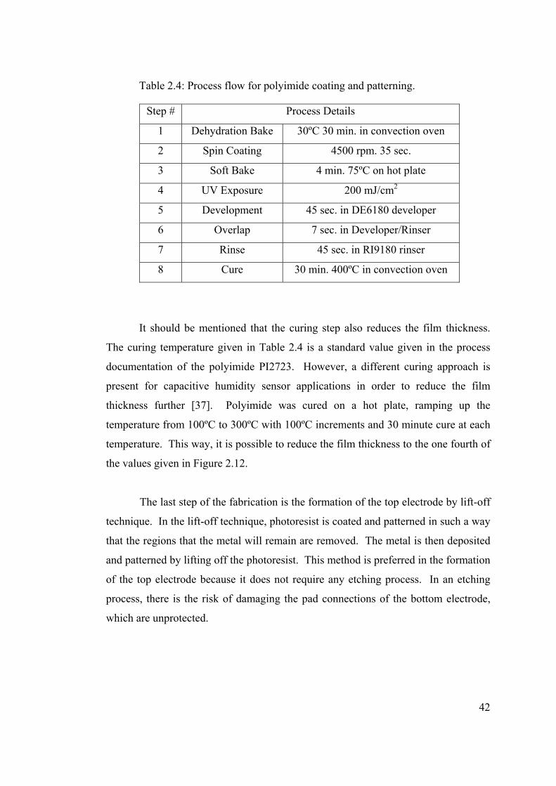
42
Table 2.4: Process flow for polyimide coating and patterning.
Step # Process Details
1 Dehydration Bake 30ºC 30 min. in convection oven
2 Spin Coating 4500 rpm. 35 sec.
3 Soft Bake 4 min. 75ºC on hot plate
4 UV Exposure 200 mJ/cm2
5 Development 45 sec. in DE6180 developer
6 Overlap 7 sec. in Developer/Rinser
7 Rinse 45 sec. in RI9180 rinser
8 Cure 30 min. 400ºC in convection oven
It should be mentioned that the curing step also reduces the film thickness.
The curing temperature given in Table 2.4 is a standard value given in the process
documentation of the polyimide PI2723. However, a different curing approach is
present for capacitive humidity sensor applications in order to reduce the film
thickness further [37]. Polyimide was cured on a hot plate, ramping up the
temperature from 100ºC to 300ºC with 100ºC increments and 30 minute cure at each
temperature. This way, it is possible to reduce the film thickness to the one fourth of
the values given in Figure 2.12.
The last step of the fabrication is the formation of the top electrode by lift-off
technique. In the lift-off technique, photoresist is coated and patterned in such a way
that the regions that the metal will remain are removed. The metal is then deposited
and patterned by lifting off the photoresist. This method is preferred in the formation
of the top electrode because it does not require any etching process. In an etching
process, there is the risk of damaging the pad connections of the bottom electrode,
which are unprotected.
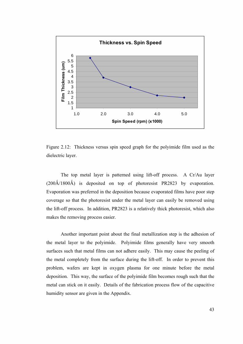
43
Thickness vs. Spin Speed
11.5
22.5
33.5
44.5
55.5
6
1.0 2.0 3.0 4.0 5.0
Spin Speed (rpm) (x1000)
Film
Thi
ckne
ss (u
m)
Figure 2.12: Thickness versus spin speed graph for the polyimide film used as the
dielectric layer.
The top metal layer is patterned using lift-off process. A Cr/Au layer
(200Ǻ/1800Ǻ) is deposited on top of photoresist PR2823 by evaporation.
Evaporation was preferred in the deposition because evaporated films have poor step
coverage so that the photoresist under the metal layer can easily be removed using
the lift-off process. In addition, PR2823 is a relatively thick photoresist, which also
makes the removing process easier.
Another important point about the final metallization step is the adhesion of
the metal layer to the polyimide. Polyimide films generally have very smooth
surfaces such that metal films can not adhere easily. This may cause the peeling of
the metal completely from the surface during the lift-off. In order to prevent this
problem, wafers are kept in oxygen plasma for one minute before the metal
deposition. This way, the surface of the polyimide film becomes rough such that the
metal can stick on it easily. Details of the fabrication process flow of the capacitive
humidity sensor are given in the Appendix.
44
2.5 Conclusion
This chapter presents the design and fabrication of a capacitive humidity
sensor with an integrated heater. The integrated heater is implemented by fabricating
the bottom electrode of the capacitive humidity sensor in a heater resistor shape.
Two types of capacitive humidity sensors are developed. Their difference is the
opening widths for moisture diffusion and dimensions of the heater electrodes.
Expected capacitances of the humidity sensors are around 30pF for 0.5µm polyimide
film thickness. The fabrication of the sensors is completed in three mask process.
Next chapter presents the design of a switched capacitor readout circuit for
capacitive humidity sensors, and Chapter 4 presents the fabrication and test results of
the capacitive humidity sensors and the readout circuit.
45
3. CHAPTER 3
THE CAPACITIVE READOUT CIRCUIT
This chapter presents the design and implementation of a switched capacitor
CMOS readout circuit for capacitive humidity sensors. Section 2.1 summarizes the
capacitive readout techniques present in the literature, including the RC oscillator,
switched capacitor integrator, and capacitance to current converter circuit structures.
Section 2.2 describes the readout circuit structure designed in this study and its
operating principle. This section also includes the design of the building blocks of
the circuit. Finally, Section 2.3 briefly explains the floor planning of mixed signal
circuits and demonstrates the layout of the chip.
3.1 Capacitive Readout Techniques
Capacitive sensors require readout circuits that convert the capacitance
change into voltage change for further signal processing of the sensor outputs. There
are various techniques of capacitance reading reported in literature. Among these
techniques, the most important ones are the RC oscillator and the switched capacitor
integrator circuits. Based on these fundamental techniques, different circuit
structures and output signal processing methods have been developed and presented
[40-44]. Following subsections explain some of these readout techniques.
CHAPTER 3
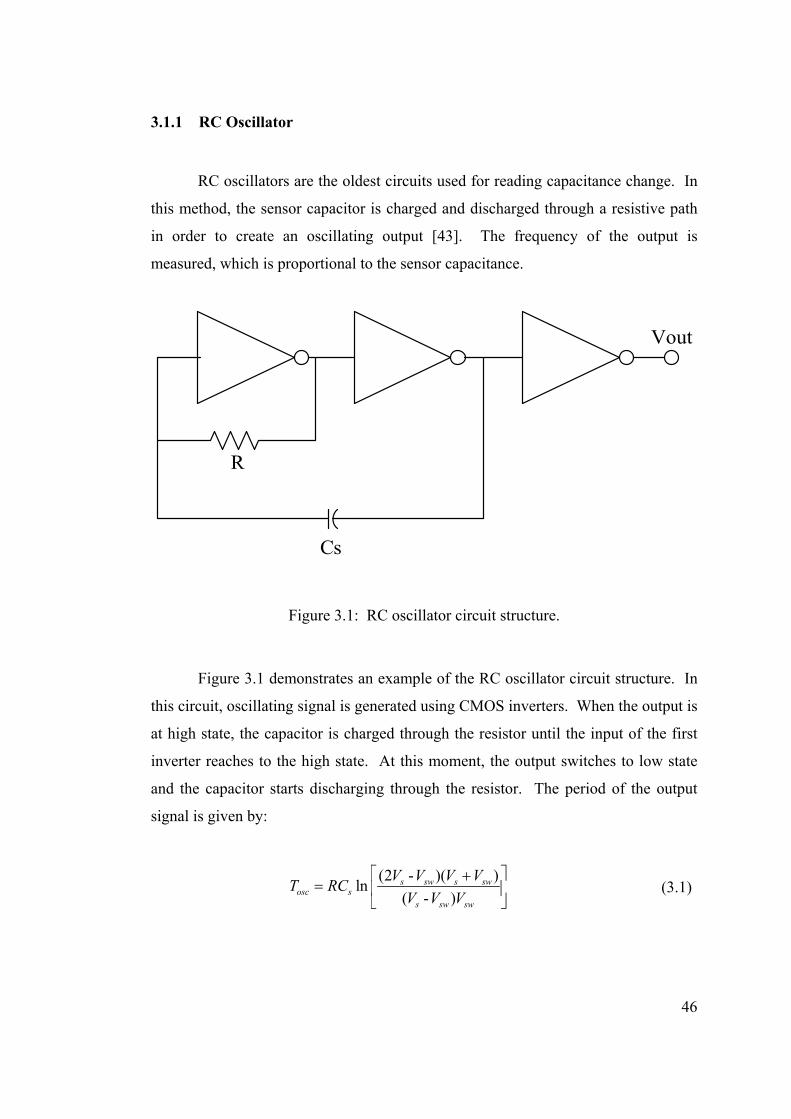
46
3.1.1 RC Oscillator
RC oscillators are the oldest circuits used for reading capacitance change. In
this method, the sensor capacitor is charged and discharged through a resistive path
in order to create an oscillating output [43]. The frequency of the output is
measured, which is proportional to the sensor capacitance.
R
Vout
Cs
Figure 3.1: RC oscillator circuit structure.
Figure 3.1 demonstrates an example of the RC oscillator circuit structure. In
this circuit, oscillating signal is generated using CMOS inverters. When the output is
at high state, the capacitor is charged through the resistor until the input of the first
inverter reaches to the high state. At this moment, the output switches to low state
and the capacitor starts discharging through the resistor. The period of the output
signal is given by:
(2 - )( )ln( - )s sw s sw
osc ss sw sw
V V V VT RCV V V
⎡ ⎤+= ⎢ ⎥
⎣ ⎦ (3.1)
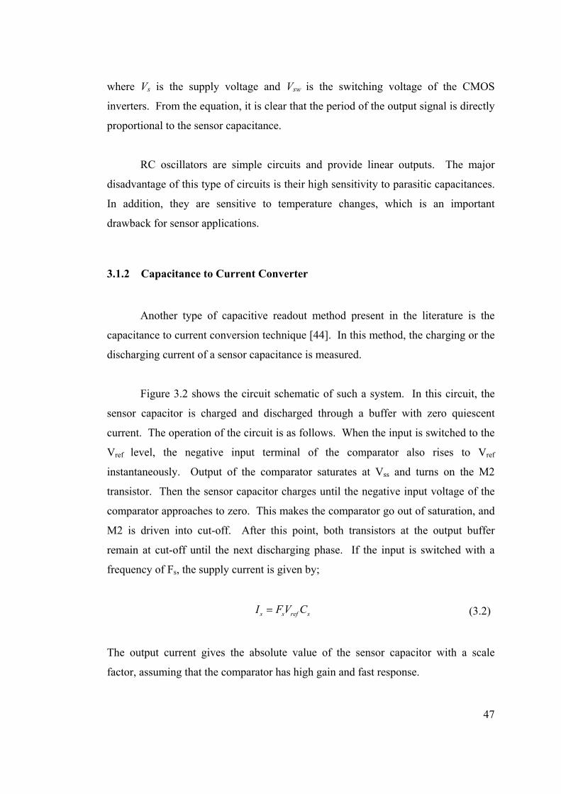
47
where Vs is the supply voltage and Vsw is the switching voltage of the CMOS
inverters. From the equation, it is clear that the period of the output signal is directly
proportional to the sensor capacitance.
RC oscillators are simple circuits and provide linear outputs. The major
disadvantage of this type of circuits is their high sensitivity to parasitic capacitances.
In addition, they are sensitive to temperature changes, which is an important
drawback for sensor applications.
3.1.2 Capacitance to Current Converter
Another type of capacitive readout method present in the literature is the
capacitance to current conversion technique [44]. In this method, the charging or the
discharging current of a sensor capacitance is measured.
Figure 3.2 shows the circuit schematic of such a system. In this circuit, the
sensor capacitor is charged and discharged through a buffer with zero quiescent
current. The operation of the circuit is as follows. When the input is switched to the
Vref level, the negative input terminal of the comparator also rises to Vref
instantaneously. Output of the comparator saturates at Vss and turns on the M2
transistor. Then the sensor capacitor charges until the negative input voltage of the
comparator approaches to zero. This makes the comparator go out of saturation, and
M2 is driven into cut-off. After this point, both transistors at the output buffer
remain at cut-off until the next discharging phase. If the input is switched with a
frequency of Fs, the supply current is given by;
s s ref sI F V C= (3.2)
The output current gives the absolute value of the sensor capacitor with a scale
factor, assuming that the comparator has high gain and fast response.
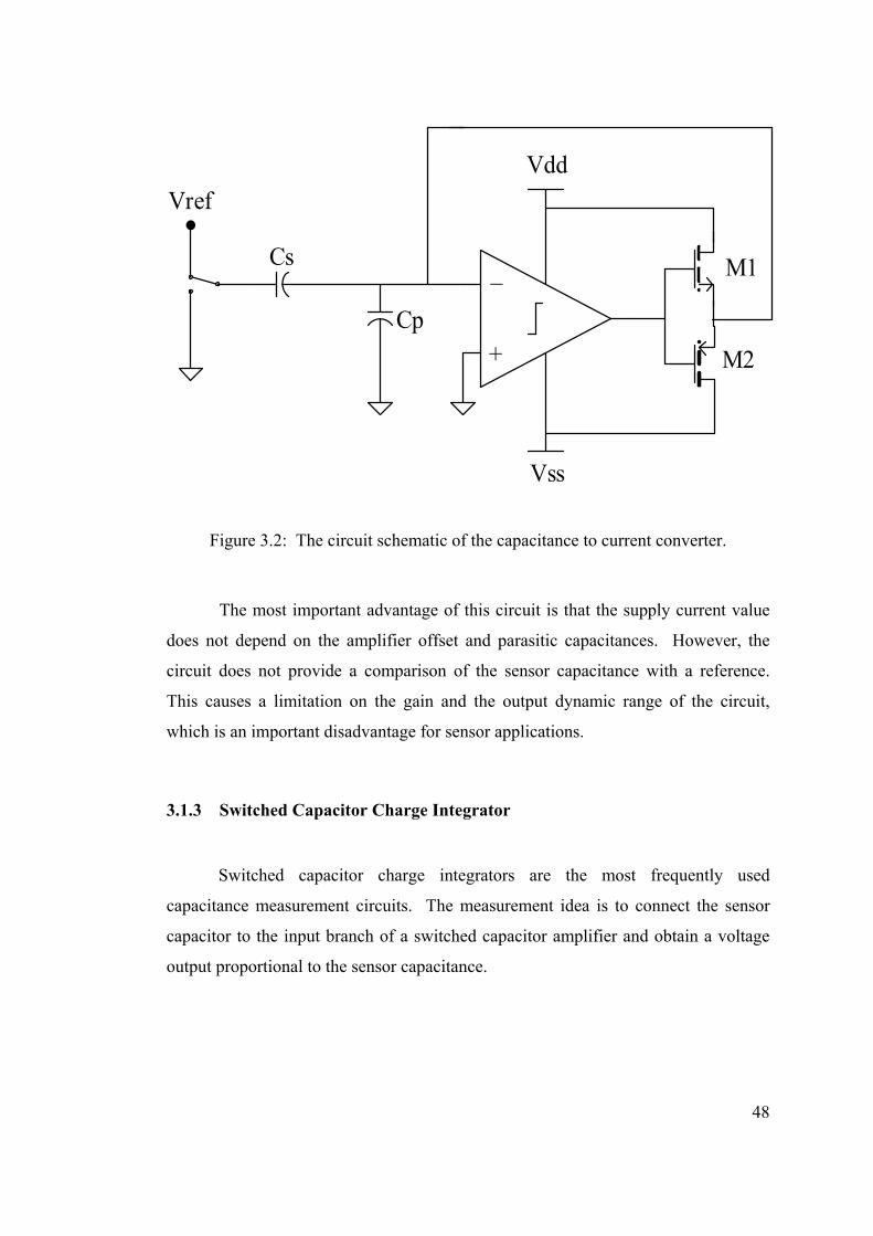
48
_
+
Vdd
Vss
Vref
Cs
Cp
M1
M2
Figure 3.2: The circuit schematic of the capacitance to current converter.
The most important advantage of this circuit is that the supply current value
does not depend on the amplifier offset and parasitic capacitances. However, the
circuit does not provide a comparison of the sensor capacitance with a reference.
This causes a limitation on the gain and the output dynamic range of the circuit,
which is an important disadvantage for sensor applications.
3.1.3 Switched Capacitor Charge Integrator
Switched capacitor charge integrators are the most frequently used
capacitance measurement circuits. The measurement idea is to connect the sensor
capacitor to the input branch of a switched capacitor amplifier and obtain a voltage
output proportional to the sensor capacitance.
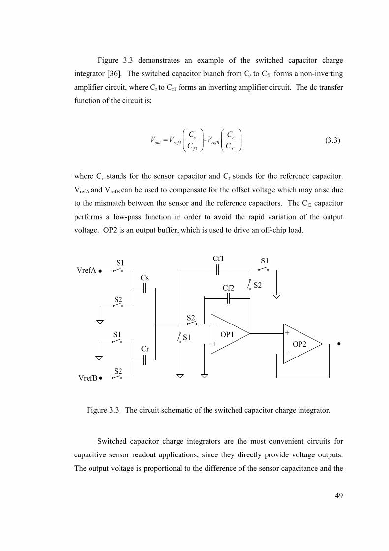
49
Figure 3.3 demonstrates an example of the switched capacitor charge
integrator [36]. The switched capacitor branch from Cs to Cf1 forms a non-inverting
amplifier circuit, where Cr to Cf1 forms an inverting amplifier circuit. The dc transfer
function of the circuit is:
1 1
-s rout refA refB
f f
C CV V VC C
⎛ ⎞ ⎛ ⎞= ⎜ ⎟ ⎜ ⎟⎜ ⎟ ⎜ ⎟
⎝ ⎠ ⎝ ⎠ (3.3)
where Cs stands for the sensor capacitor and Cr stands for the reference capacitor.
VrefA and VrefB can be used to compensate for the offset voltage which may arise due
to the mismatch between the sensor and the reference capacitors. The Cf2 capacitor
performs a low-pass function in order to avoid the rapid variation of the output
voltage. OP2 is an output buffer, which is used to drive an off-chip load.
_
+_
+
Cs
Cr
Cf1
Cf2
OP1OP2
VrefA
VrefB
S1
S1
S1
S1
S2
S2
S2
S2
Figure 3.3: The circuit schematic of the switched capacitor charge integrator.
Switched capacitor charge integrators are the most convenient circuits for
capacitive sensor readout applications, since they directly provide voltage outputs.
The output voltage is proportional to the difference of the sensor capacitance and the
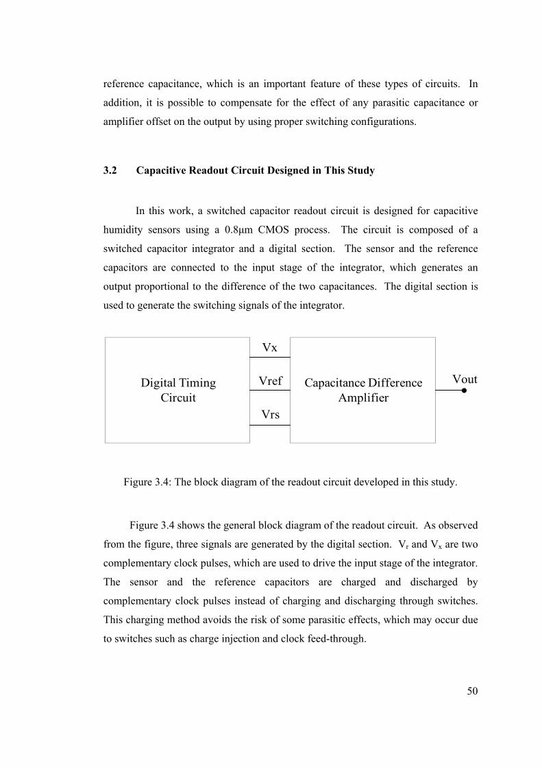
50
reference capacitance, which is an important feature of these types of circuits. In
addition, it is possible to compensate for the effect of any parasitic capacitance or
amplifier offset on the output by using proper switching configurations.
3.2 Capacitive Readout Circuit Designed in This Study
In this work, a switched capacitor readout circuit is designed for capacitive
humidity sensors using a 0.8µm CMOS process. The circuit is composed of a
switched capacitor integrator and a digital section. The sensor and the reference
capacitors are connected to the input stage of the integrator, which generates an
output proportional to the difference of the two capacitances. The digital section is
used to generate the switching signals of the integrator.
Capacitance DifferenceAmplifier
Digital TimingCircuit
Vx
Vref
Vrs
Vout
Figure 3.4: The block diagram of the readout circuit developed in this study.
Figure 3.4 shows the general block diagram of the readout circuit. As observed
from the figure, three signals are generated by the digital section. Vr and Vx are two
complementary clock pulses, which are used to drive the input stage of the integrator.
The sensor and the reference capacitors are charged and discharged by
complementary clock pulses instead of charging and discharging through switches.
This charging method avoids the risk of some parasitic effects, which may occur due
to switches such as charge injection and clock feed-through.
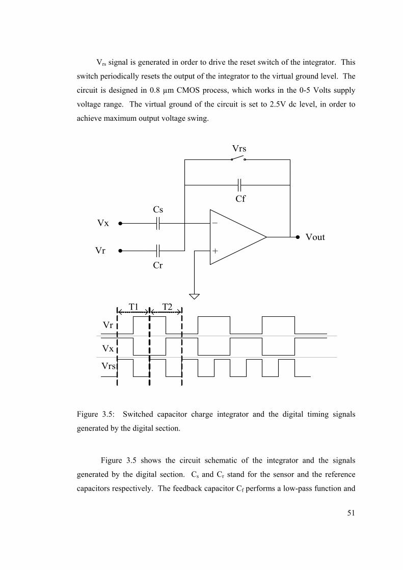
51
Vrs signal is generated in order to drive the reset switch of the integrator. This
switch periodically resets the output of the integrator to the virtual ground level. The
circuit is designed in 0.8 µm CMOS process, which works in the 0-5 Volts supply
voltage range. The virtual ground of the circuit is set to 2.5V dc level, in order to
achieve maximum output voltage swing.
Vx
VrVout
Cf
_
+
Cs
Cr
Vrs
Vx
Vr
Vrs
T1 T2
Figure 3.5: Switched capacitor charge integrator and the digital timing signals
generated by the digital section.
Figure 3.5 shows the circuit schematic of the integrator and the signals
generated by the digital section. Cs and Cr stand for the sensor and the reference
capacitors respectively. The feedback capacitor Cf performs a low-pass function and
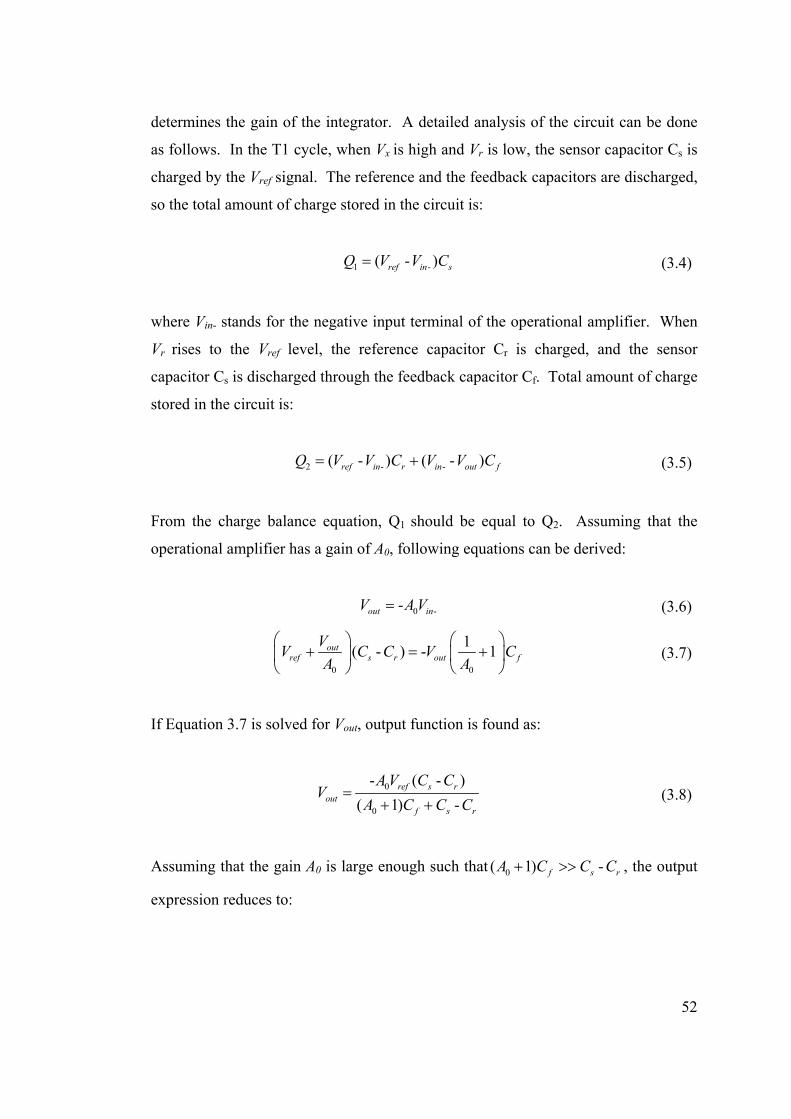
52
determines the gain of the integrator. A detailed analysis of the circuit can be done
as follows. In the T1 cycle, when Vx is high and Vr is low, the sensor capacitor Cs is
charged by the Vref signal. The reference and the feedback capacitors are discharged,
so the total amount of charge stored in the circuit is:
1 -( - )ref in sQ V V C= (3.4)
where Vin- stands for the negative input terminal of the operational amplifier. When
Vr rises to the Vref level, the reference capacitor Cr is charged, and the sensor
capacitor Cs is discharged through the feedback capacitor Cf. Total amount of charge
stored in the circuit is:
2 - -( - ) ( - )ref in r in out fQ V V C V V C= + (3.5)
From the charge balance equation, Q1 should be equal to Q2. Assuming that the
operational amplifier has a gain of A0, following equations can be derived:
0 --out inV A V= (3.6)
0 0
1( - ) - 1outref s r out f
VV C C V CA A
⎛ ⎞ ⎛ ⎞+ = +⎜ ⎟ ⎜ ⎟
⎝ ⎠ ⎝ ⎠ (3.7)
If Equation 3.7 is solved for Vout, output function is found as:
0
0
- ( - )( 1) -
ref s rout
f s r
A V C CV
A C C C=
+ + (3.8)
Assuming that the gain A0 is large enough such that 0( 1) -f s rA C C C+ >> , the output
expression reduces to:
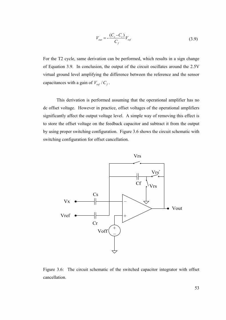
53
( - )- s rout ref
f
C CV VC
= (3.9)
For the T2 cycle, same derivation can be performed, which results in a sign change
of Equation 3.9. In conclusion, the output of the circuit oscillates around the 2.5V
virtual ground level amplifying the difference between the reference and the sensor
capacitances with a gain of /ref fV C .
This derivation is performed assuming that the operational amplifier has no
dc offset voltage. However in practice, offset voltages of the operational amplifiers
significantly affect the output voltage level. A simple way of removing this effect is
to store the offset voltage on the feedback capacitor and subtract it from the output
by using proper switching configuration. Figure 3.6 shows the circuit schematic with
switching configuration for offset cancellation.
Vrs
Vx
VrefVout
Cf
_
+
Cs
Cr
Vrs
Vrs´
+_Voff
Figure 3.6: The circuit schematic of the switched capacitor integrator with offset
cancellation.
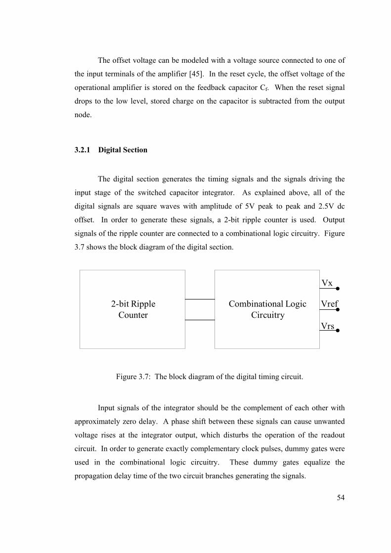
54
The offset voltage can be modeled with a voltage source connected to one of
the input terminals of the amplifier [45]. In the reset cycle, the offset voltage of the
operational amplifier is stored on the feedback capacitor Cf. When the reset signal
drops to the low level, stored charge on the capacitor is subtracted from the output
node.
3.2.1 Digital Section
The digital section generates the timing signals and the signals driving the
input stage of the switched capacitor integrator. As explained above, all of the
digital signals are square waves with amplitude of 5V peak to peak and 2.5V dc
offset. In order to generate these signals, a 2-bit ripple counter is used. Output
signals of the ripple counter are connected to a combinational logic circuitry. Figure
3.7 shows the block diagram of the digital section.
Combinational LogicCircuitry
2-bit RippleCounter
Vx
Vref
Vrs
Figure 3.7: The block diagram of the digital timing circuit.
Input signals of the integrator should be the complement of each other with
approximately zero delay. A phase shift between these signals can cause unwanted
voltage rises at the integrator output, which disturbs the operation of the readout
circuit. In order to generate exactly complementary clock pulses, dummy gates were
used in the combinational logic circuitry. These dummy gates equalize the
propagation delay time of the two circuit branches generating the signals.
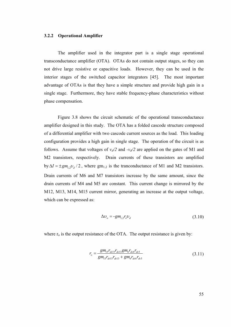
55
3.2.2 Operational Amplifier
The amplifier used in the integrator part is a single stage operational
transconductance amplifier (OTA). OTAs do not contain output stages, so they can
not drive large resistive or capacitive loads. However, they can be used in the
interior stages of the switched capacitor integrators [45]. The most important
advantage of OTAs is that they have a simple structure and provide high gain in a
single stage. Furthermore, they have stable frequency-phase characteristics without
phase compensation.
Figure 3.8 shows the circuit schematic of the operational transconductance
amplifier designed in this study. The OTA has a folded cascode structure composed
of a differential amplifier with two cascode current sources as the load. This loading
configuration provides a high gain in single stage. The operation of the circuit is as
follows. Assume that voltages of νd/2 and -νd/2 are applied on the gates of M1 and
M2 transistors, respectively. Drain currents of these transistors are amplified
by 1,2 / 2dI gm υ∆ = ± , where gm1,2 is the tranconductance of M1 and M2 transistors.
Drain currents of M6 and M7 transistors increase by the same amount, since the
drain currents of M4 and M5 are constant. This current change is mirrored by the
M12, M13, M14, M15 current mirror, generating an increase at the output voltage,
which can be expressed as:
1,2-o o dgm rυ υ∆ = (3.10)
where ro is the output resistance of the OTA. The output resistance is given by:
15 15 13 6 6 5
15 15 13 6 6 5
ds ds ds dso
ds ds ds ds
gm r r gm r rrgm r r gm r r
=+
(3.11)
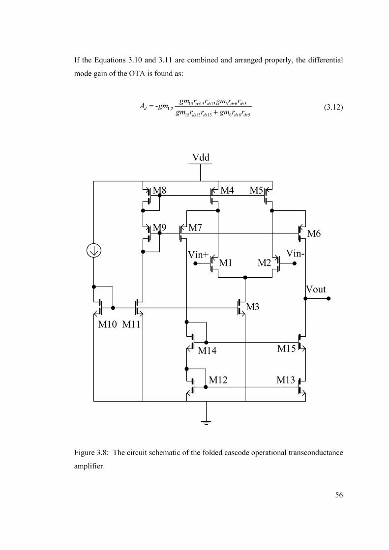
56
If the Equations 3.10 and 3.11 are combined and arranged properly, the differential
mode gain of the OTA is found as:
15 15 13 6 6 51,2
15 15 13 6 6 5
- ds ds ds dsd
ds ds ds ds
gm r r gm r rA gmgm r r gm r r
=+
(3.12)
Vout
Vin-Vin+M1 M2
M3
M4 M5
M6M7
M8
M9
M10 M11
M12 M13
M14 M15
Vdd
Figure 3.8: The circuit schematic of the folded cascode operational transconductance
amplifier.
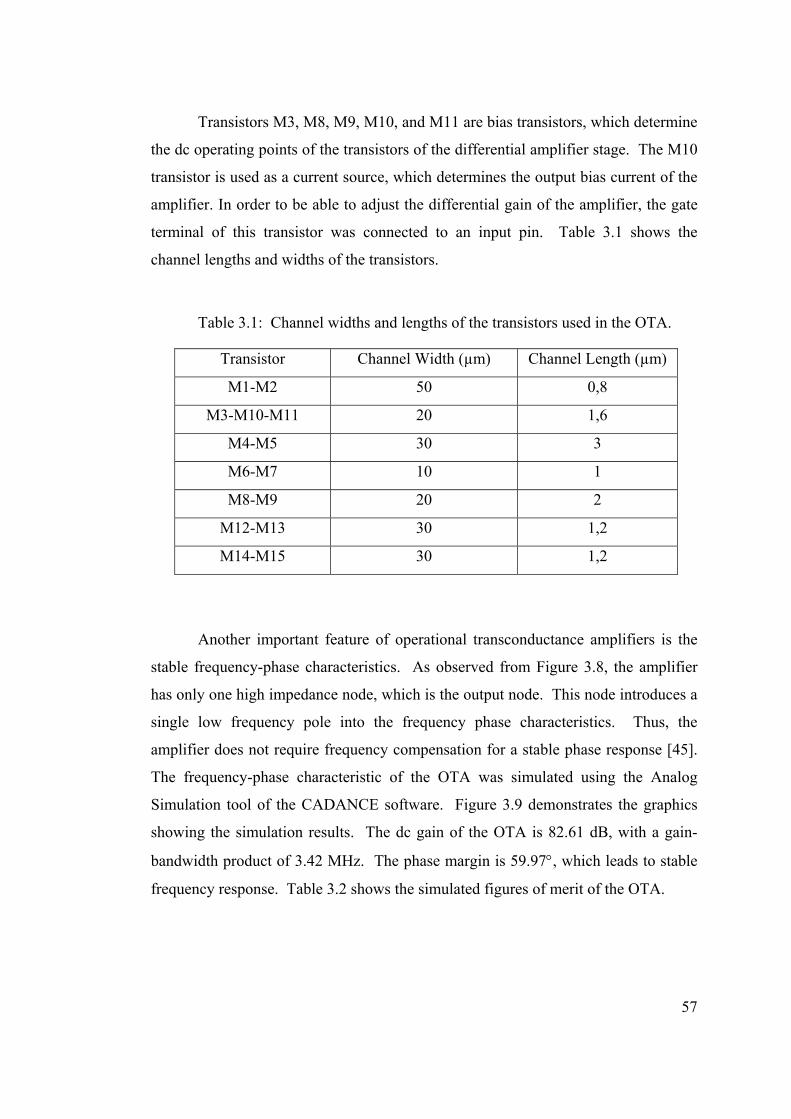
57
Transistors M3, M8, M9, M10, and M11 are bias transistors, which determine
the dc operating points of the transistors of the differential amplifier stage. The M10
transistor is used as a current source, which determines the output bias current of the
amplifier. In order to be able to adjust the differential gain of the amplifier, the gate
terminal of this transistor was connected to an input pin. Table 3.1 shows the
channel lengths and widths of the transistors.
Table 3.1: Channel widths and lengths of the transistors used in the OTA.
Transistor Channel Width (µm) Channel Length (µm)
M1-M2 50 0,8
M3-M10-M11 20 1,6
M4-M5 30 3
M6-M7 10 1
M8-M9 20 2
M12-M13 30 1,2
M14-M15 30 1,2
Another important feature of operational transconductance amplifiers is the
stable frequency-phase characteristics. As observed from Figure 3.8, the amplifier
has only one high impedance node, which is the output node. This node introduces a
single low frequency pole into the frequency phase characteristics. Thus, the
amplifier does not require frequency compensation for a stable phase response [45].
The frequency-phase characteristic of the OTA was simulated using the Analog
Simulation tool of the CADANCE software. Figure 3.9 demonstrates the graphics
showing the simulation results. The dc gain of the OTA is 82.61 dB, with a gain-
bandwidth product of 3.42 MHz. The phase margin is 59.97°, which leads to stable
frequency response. Table 3.2 shows the simulated figures of merit of the OTA.
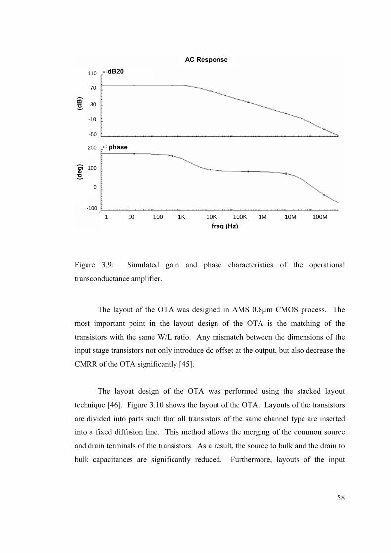
58
AC Response
dB20
1 10 100 1K 10K 100K 1M 10M 100M
110
70
30
-10
-50
200
100
0
-100
phase
(d
eg)
(dB
)
freq (Hz)
Figure 3.9: Simulated gain and phase characteristics of the operational
transconductance amplifier.
The layout of the OTA was designed in AMS 0.8µm CMOS process. The
most important point in the layout design of the OTA is the matching of the
transistors with the same W/L ratio. Any mismatch between the dimensions of the
input stage transistors not only introduce dc offset at the output, but also decrease the
CMRR of the OTA significantly [45].
The layout design of the OTA was performed using the stacked layout
technique [46]. Figure 3.10 shows the layout of the OTA. Layouts of the transistors
are divided into parts such that all transistors of the same channel type are inserted
into a fixed diffusion line. This method allows the merging of the common source
and drain terminals of the transistors. As a result, the source to bulk and the drain to
bulk capacitances are significantly reduced. Furthermore, layouts of the input
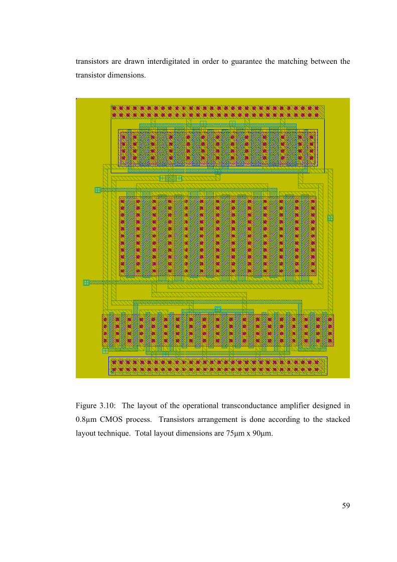
59
transistors are drawn interdigitated in order to guarantee the matching between the
transistor dimensions.
Figure 3.10: The layout of the operational transconductance amplifier designed in
0.8µm CMOS process. Transistors arrangement is done according to the stacked
layout technique. Total layout dimensions are 75µm x 90µm.
60
Table 3.2: Simulated figures of merit for the operational transconductance amplifier.
Parameter Value
DC gain 82.61 dB
Gain-bandwidth product 3.42 MHz
Phase margin 59.97°
CMMR 132.91dB
3-dB bandwidth 41.12 kHz
3.2.3 Floor Plan and Layout
The switched capacitor integrator is a mixed signal circuit composed of
analog and digital blocks. In mixed signal circuits, there is a wide variety of noise
sources affecting the output signal [46]. Therefore, floor planning of mixed signal
circuit layouts are extremely important in the performance of the fabricated circuit.
The most important type of digital noise coupling is the capacitive coupling
[46]. Capacitive coupling occurs between the analog and digital signal busses
especially when they are routed close to each other. In order to prevent this type of
coupling, analog and digital blocks were placed far away from each other.
Capacitors and switches were placed between the analog and the digital sections.
Further protection against the digital noise coupling is achieved by guard
rings surrounding the main blocks of the circuit. It is possible to implement guard
rings in two ways. One is the n-well contact, which is biased to the positive supply
voltage level. This type of guard ring provides a surface barrier for the noisy
currents. The other way is to place substrate contacts around the block to be
protected. Substrate contacts are connected to the ground of the circuit in order to
provide a low impedance path for noisy currents. The digital section was protected
by a double guard ring composed of both the n-well contact and the substrate contact.
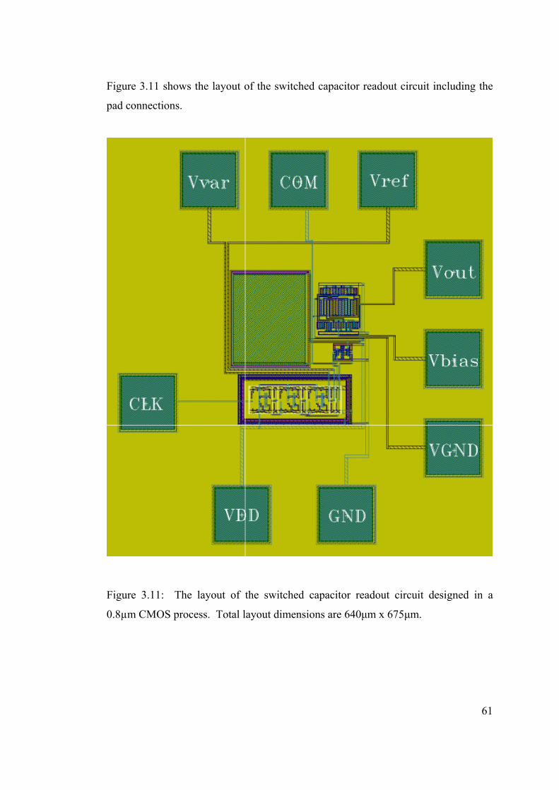
61
Figure 3.11 shows the layout of the switched capacitor readout circuit including the
pad connections.
Figure 3.11: The layout of the switched capacitor readout circuit designed in a
0.8µm CMOS process. Total layout dimensions are 640µm x 675µm.
62
3.3 Conclusion
This chapter presents the design of a switched capacitor readout circuit for
capacitive humidity sensors. The circuit is composed of a switched capacitor
integrator and a digital timing circuit used for the generation of the signals driving
the integrator. The layout of the circuit was designed in the AMS 0.8µm CMOS
process. Next chapter presents the fabrication and test results of the capacitive
humidity sensors and the hybrid humidity sensor module.
63
4. CHAPTER 4
FABRICATION AND TEST RESULTS
This chapter presents the fabrication and test results of the capacitive
humidity sensor and the switched capacitor readout circuit. Section 4.1 demonstrates
the fabricated capacitive humidity sensors and results of some initial measurements.
Section 4.2 gives the characterization results of the capacitive humidity sensors.
This section presents the humidity response, hysteresis characteristics, temperature
dependency of the humidity response, and the response time measurements. Section
4.3 explains the tests performed on the integrated heater. This section presents the
effect of heating on the sensor response. Section 4.4 presents the hybrid humidity
sensor module, which is obtained by wire bonding the humidity sensor directly to the
readout circuit. This section also gives the test results on the hybrid humidity sensor
module.
4.1 Fabrication Results
Capacitive humidity sensors are fabricated by three mask process as
explained in Section 2.4. Figure 4.1 shows the SEM pictures of the fabricated
capacitive humidity sensors with the heater electrodes.
CHAPTER 4
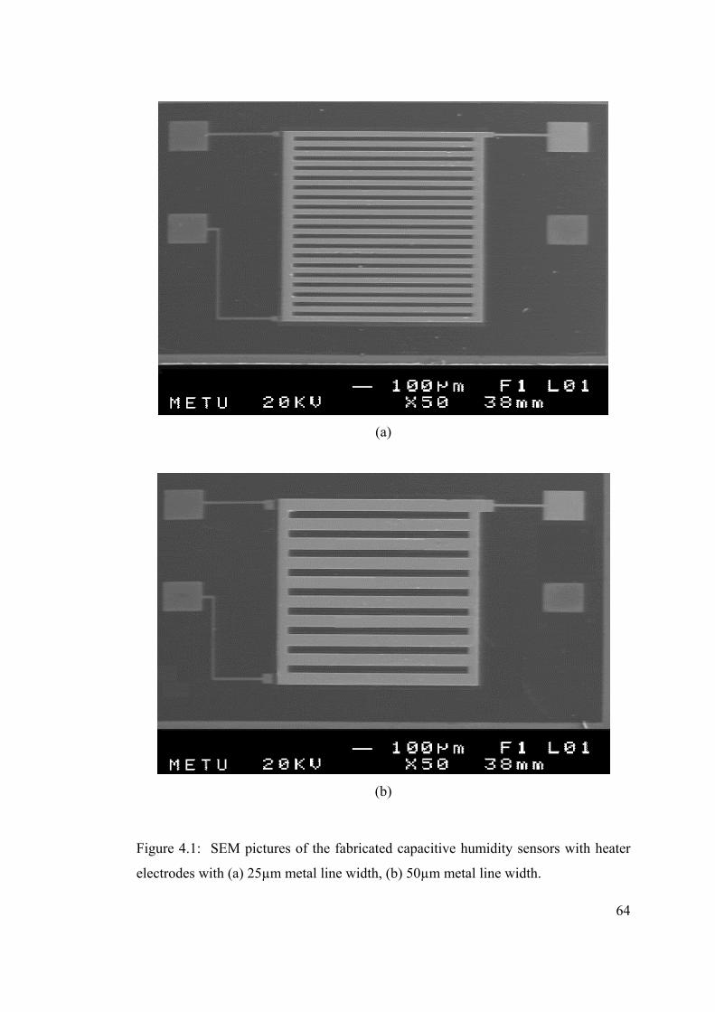
64
(a)
(b)
Figure 4.1: SEM pictures of the fabricated capacitive humidity sensors with heater
electrodes with (a) 25µm metal line width, (b) 50µm metal line width.
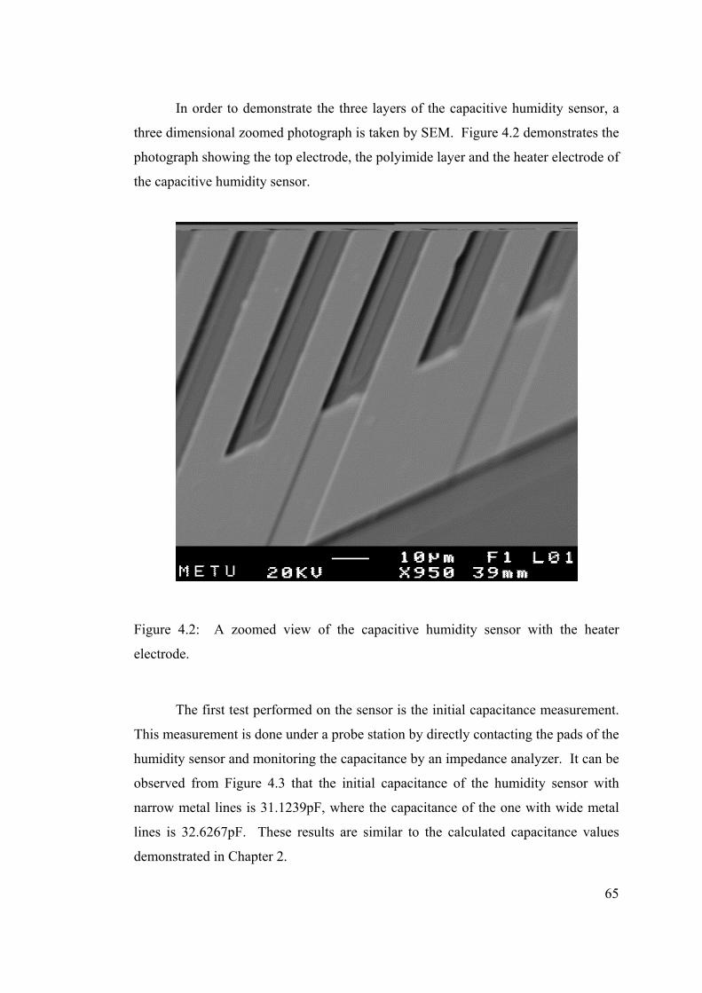
65
In order to demonstrate the three layers of the capacitive humidity sensor, a
three dimensional zoomed photograph is taken by SEM. Figure 4.2 demonstrates the
photograph showing the top electrode, the polyimide layer and the heater electrode of
the capacitive humidity sensor.
Figure 4.2: A zoomed view of the capacitive humidity sensor with the heater
electrode.
The first test performed on the sensor is the initial capacitance measurement.
This measurement is done under a probe station by directly contacting the pads of the
humidity sensor and monitoring the capacitance by an impedance analyzer. It can be
observed from Figure 4.3 that the initial capacitance of the humidity sensor with
narrow metal lines is 31.1239pF, where the capacitance of the one with wide metal
lines is 32.6267pF. These results are similar to the calculated capacitance values
demonstrated in Chapter 2.
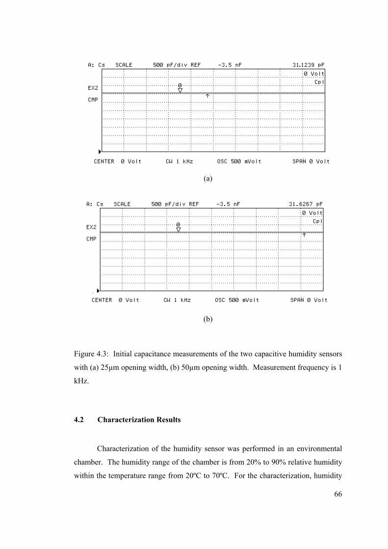
66
(a)
(b)
Figure 4.3: Initial capacitance measurements of the two capacitive humidity sensors
with (a) 25µm opening width, (b) 50µm opening width. Measurement frequency is 1
kHz.
4.2 Characterization Results
Characterization of the humidity sensor was performed in an environmental
chamber. The humidity range of the chamber is from 20% to 90% relative humidity
within the temperature range from 20ºC to 70ºC. For the characterization, humidity
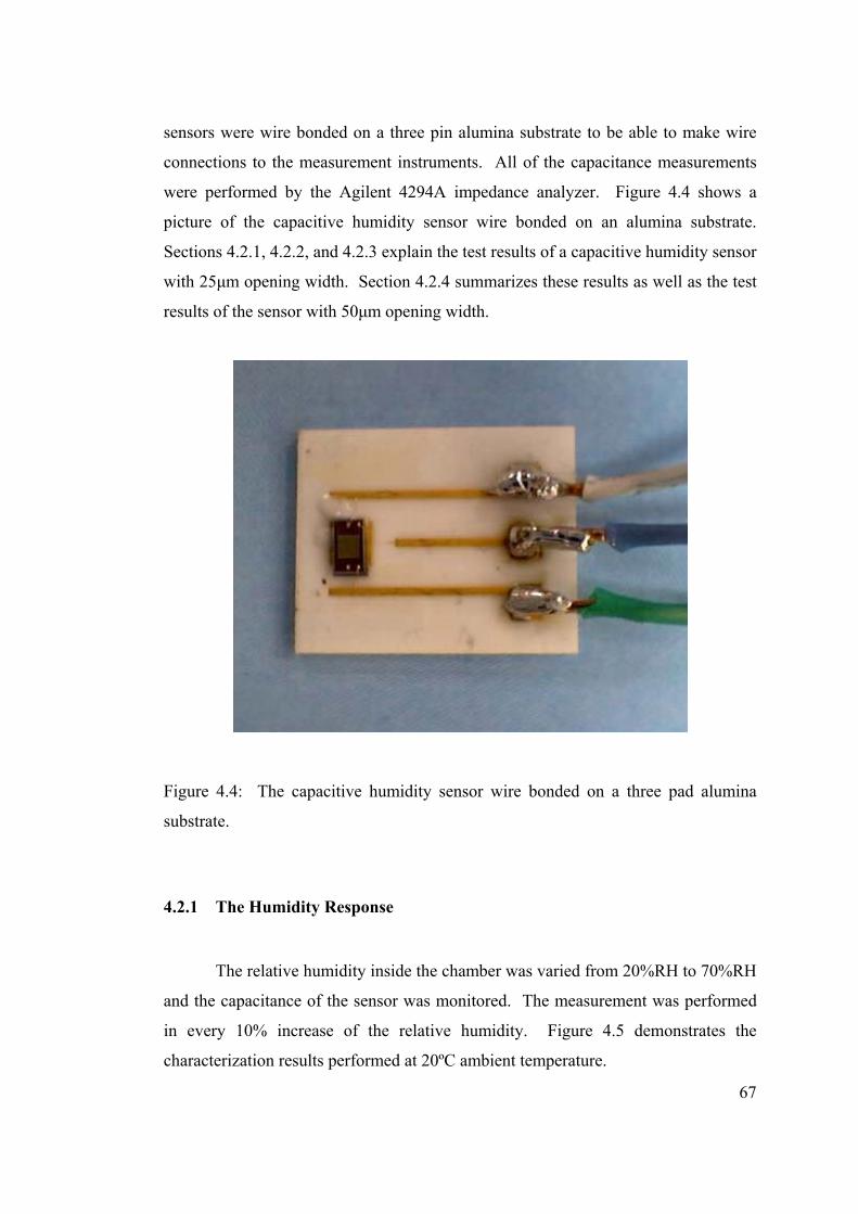
67
sensors were wire bonded on a three pin alumina substrate to be able to make wire
connections to the measurement instruments. All of the capacitance measurements
were performed by the Agilent 4294A impedance analyzer. Figure 4.4 shows a
picture of the capacitive humidity sensor wire bonded on an alumina substrate.
Sections 4.2.1, 4.2.2, and 4.2.3 explain the test results of a capacitive humidity sensor
with 25µm opening width. Section 4.2.4 summarizes these results as well as the test
results of the sensor with 50µm opening width.
Figure 4.4: The capacitive humidity sensor wire bonded on a three pad alumina
substrate.
4.2.1 The Humidity Response
The relative humidity inside the chamber was varied from 20%RH to 70%RH
and the capacitance of the sensor was monitored. The measurement was performed
in every 10% increase of the relative humidity. Figure 4.5 demonstrates the
characterization results performed at 20ºC ambient temperature.
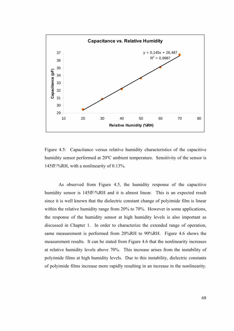
68
Capacitance vs. Relative Humidity
y = 0,145x + 26,487R2 = 0,9987
29
30
31
32
33
34
35
36
37
10 20 30 40 50 60 70 80
Relative Humidity (%RH)
Capa
cita
nce
(pF)
Figure 4.5: Capacitance versus relative humidity characteristics of the capacitive
humidity sensor performed at 20ºC ambient temperature. Sensitivity of the sensor is
145fF/%RH, with a nonlinearity of 0.13%.
As observed from Figure 4.5, the humidity response of the capacitive
humidity sensor is 145fF/%RH and it is almost linear. This is an expected result
since it is well known that the dielectric constant change of polyimide film is linear
within the relative humidity range from 20% to 70%. However in some applications,
the response of the humidity sensor at high humidity levels is also important as
discussed in Chapter 1. In order to characterize the extended range of operation,
same measurement is performed from 20%RH to 90%RH. Figure 4.6 shows the
measurement results. It can be stated from Figure 4.6 that the nonlinearity increases
at relative humidity levels above 70%. This increase arises from the instability of
polyimide films at high humidity levels. Due to this instability, dielectric constants
of polyimide films increase more rapidly resulting in an increase in the nonlinearity.
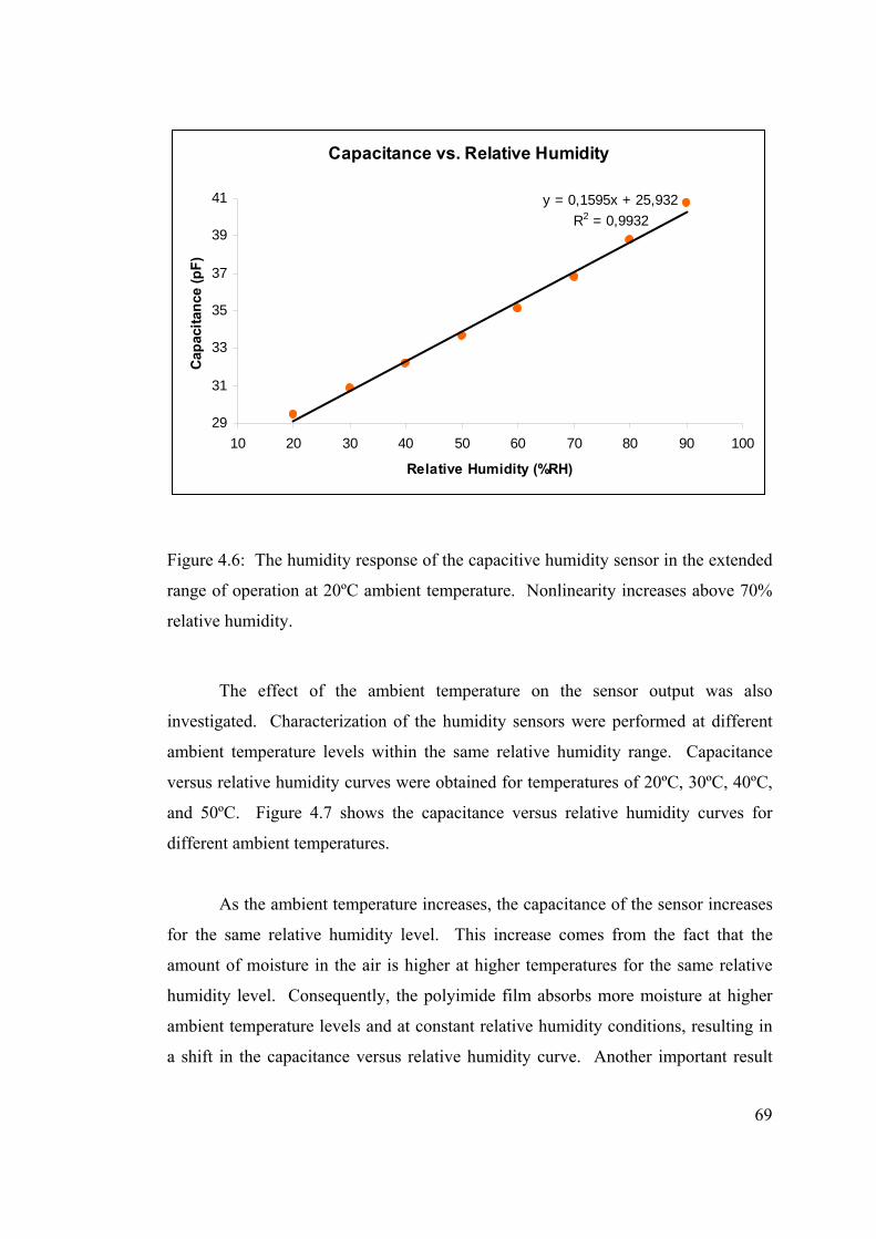
69
Capacitance vs. Relative Humidity
y = 0,1595x + 25,932R2 = 0,9932
29
31
33
35
37
39
41
10 20 30 40 50 60 70 80 90 100
Relative Humidity (%RH)
Capa
cita
nce
(pF)
Figure 4.6: The humidity response of the capacitive humidity sensor in the extended
range of operation at 20ºC ambient temperature. Nonlinearity increases above 70%
relative humidity.
The effect of the ambient temperature on the sensor output was also
investigated. Characterization of the humidity sensors were performed at different
ambient temperature levels within the same relative humidity range. Capacitance
versus relative humidity curves were obtained for temperatures of 20ºC, 30ºC, 40ºC,
and 50ºC. Figure 4.7 shows the capacitance versus relative humidity curves for
different ambient temperatures.
As the ambient temperature increases, the capacitance of the sensor increases
for the same relative humidity level. This increase comes from the fact that the
amount of moisture in the air is higher at higher temperatures for the same relative
humidity level. Consequently, the polyimide film absorbs more moisture at higher
ambient temperature levels and at constant relative humidity conditions, resulting in
a shift in the capacitance versus relative humidity curve. Another important result
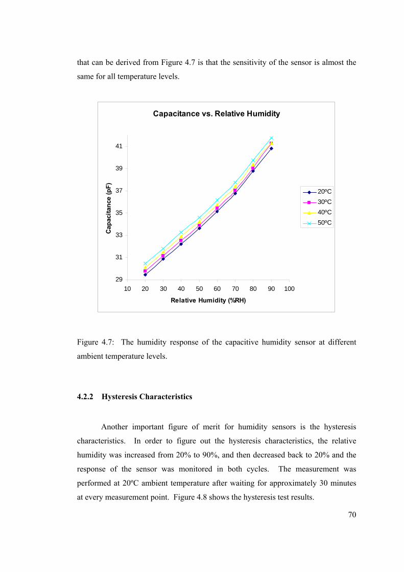
70
that can be derived from Figure 4.7 is that the sensitivity of the sensor is almost the
same for all temperature levels.
Capacitance vs. Relative Humidity
29
31
33
35
37
39
41
10 20 30 40 50 60 70 80 90 100
Relative Humidity (%RH)
Capa
cita
nce
(pF)
20ºC30ºC40ºC50ºC
Figure 4.7: The humidity response of the capacitive humidity sensor at different
ambient temperature levels.
4.2.2 Hysteresis Characteristics
Another important figure of merit for humidity sensors is the hysteresis
characteristics. In order to figure out the hysteresis characteristics, the relative
humidity was increased from 20% to 90%, and then decreased back to 20% and the
response of the sensor was monitored in both cycles. The measurement was
performed at 20ºC ambient temperature after waiting for approximately 30 minutes
at every measurement point. Figure 4.8 shows the hysteresis test results.
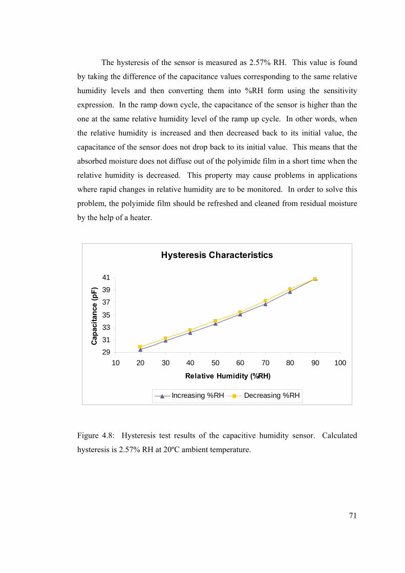
71
The hysteresis of the sensor is measured as 2.57% RH. This value is found
by taking the difference of the capacitance values corresponding to the same relative
humidity levels and then converting them into %RH form using the sensitivity
expression. In the ramp down cycle, the capacitance of the sensor is higher than the
one at the same relative humidity level of the ramp up cycle. In other words, when
the relative humidity is increased and then decreased back to its initial value, the
capacitance of the sensor does not drop back to its initial value. This means that the
absorbed moisture does not diffuse out of the polyimide film in a short time when the
relative humidity is decreased. This property may cause problems in applications
where rapid changes in relative humidity are to be monitored. In order to solve this
problem, the polyimide film should be refreshed and cleaned from residual moisture
by the help of a heater.
Hysteresis Characteristics
29
31
33
35
37
39
41
10 20 30 40 50 60 70 80 90 100
Relative Humidity (%RH)
Cap
acita
nce
(pF)
Increasing %RH Decreasing %RH
Figure 4.8: Hysteresis test results of the capacitive humidity sensor. Calculated
hysteresis is 2.57% RH at 20ºC ambient temperature.
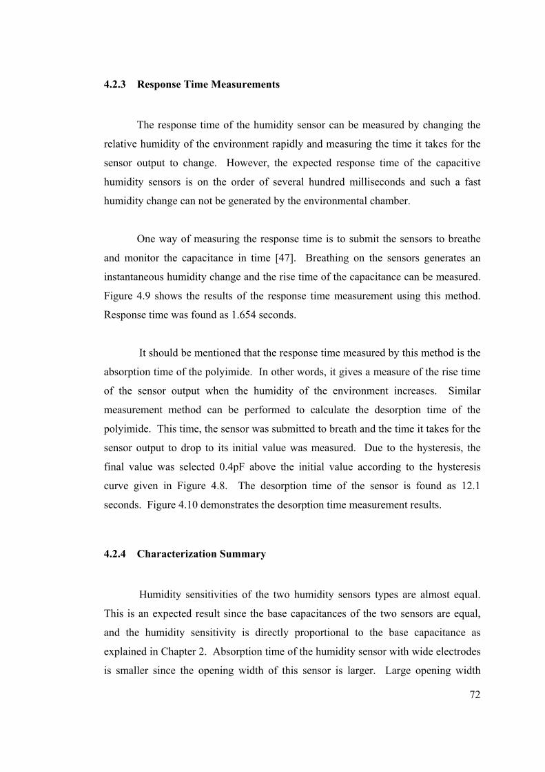
72
4.2.3 Response Time Measurements
The response time of the humidity sensor can be measured by changing the
relative humidity of the environment rapidly and measuring the time it takes for the
sensor output to change. However, the expected response time of the capacitive
humidity sensors is on the order of several hundred milliseconds and such a fast
humidity change can not be generated by the environmental chamber.
One way of measuring the response time is to submit the sensors to breathe
and monitor the capacitance in time [47]. Breathing on the sensors generates an
instantaneous humidity change and the rise time of the capacitance can be measured.
Figure 4.9 shows the results of the response time measurement using this method.
Response time was found as 1.654 seconds.
It should be mentioned that the response time measured by this method is the
absorption time of the polyimide. In other words, it gives a measure of the rise time
of the sensor output when the humidity of the environment increases. Similar
measurement method can be performed to calculate the desorption time of the
polyimide. This time, the sensor was submitted to breath and the time it takes for the
sensor output to drop to its initial value was measured. Due to the hysteresis, the
final value was selected 0.4pF above the initial value according to the hysteresis
curve given in Figure 4.8. The desorption time of the sensor is found as 12.1
seconds. Figure 4.10 demonstrates the desorption time measurement results.
4.2.4 Characterization Summary
Humidity sensitivities of the two humidity sensors types are almost equal.
This is an expected result since the base capacitances of the two sensors are equal,
and the humidity sensitivity is directly proportional to the base capacitance as
explained in Chapter 2. Absorption time of the humidity sensor with wide electrodes
is smaller since the opening width of this sensor is larger. Large opening width
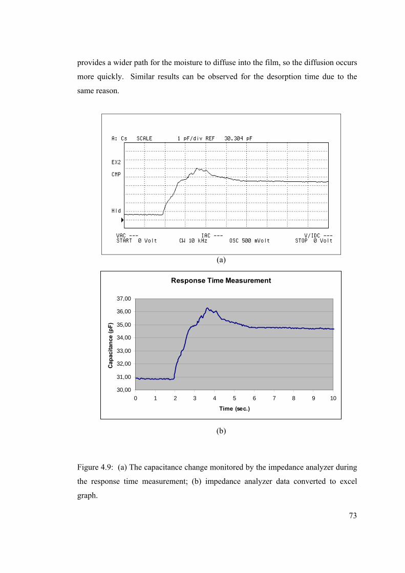
73
provides a wider path for the moisture to diffuse into the film, so the diffusion occurs
more quickly. Similar results can be observed for the desorption time due to the
same reason.
(a)
Response Time Measurement
30,00
31,00
32,00
33,00
34,00
35,00
36,00
37,00
0 1 2 3 4 5 6 7 8 9 10
Time (sec.)
Capa
cita
nce
(pF)
(b)
Figure 4.9: (a) The capacitance change monitored by the impedance analyzer during
the response time measurement; (b) impedance analyzer data converted to excel
graph.
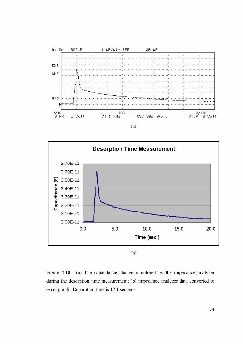
74
(a)
Desorption Time Measurement
3.00E-11
3.10E-11
3.20E-11
3.30E-11
3.40E-11
3.50E-11
3.60E-11
3.70E-11
0.0 5.0 10.0 15.0 20.0
Time (sec.)
Cap
acita
nce
(F)
(b)
Figure 4.10: (a) The capacitance change monitored by the impedance analyzer
during the desorption time measurement; (b) impedance analyzer data converted to
excel graph. Desorption time is 12.1 seconds.
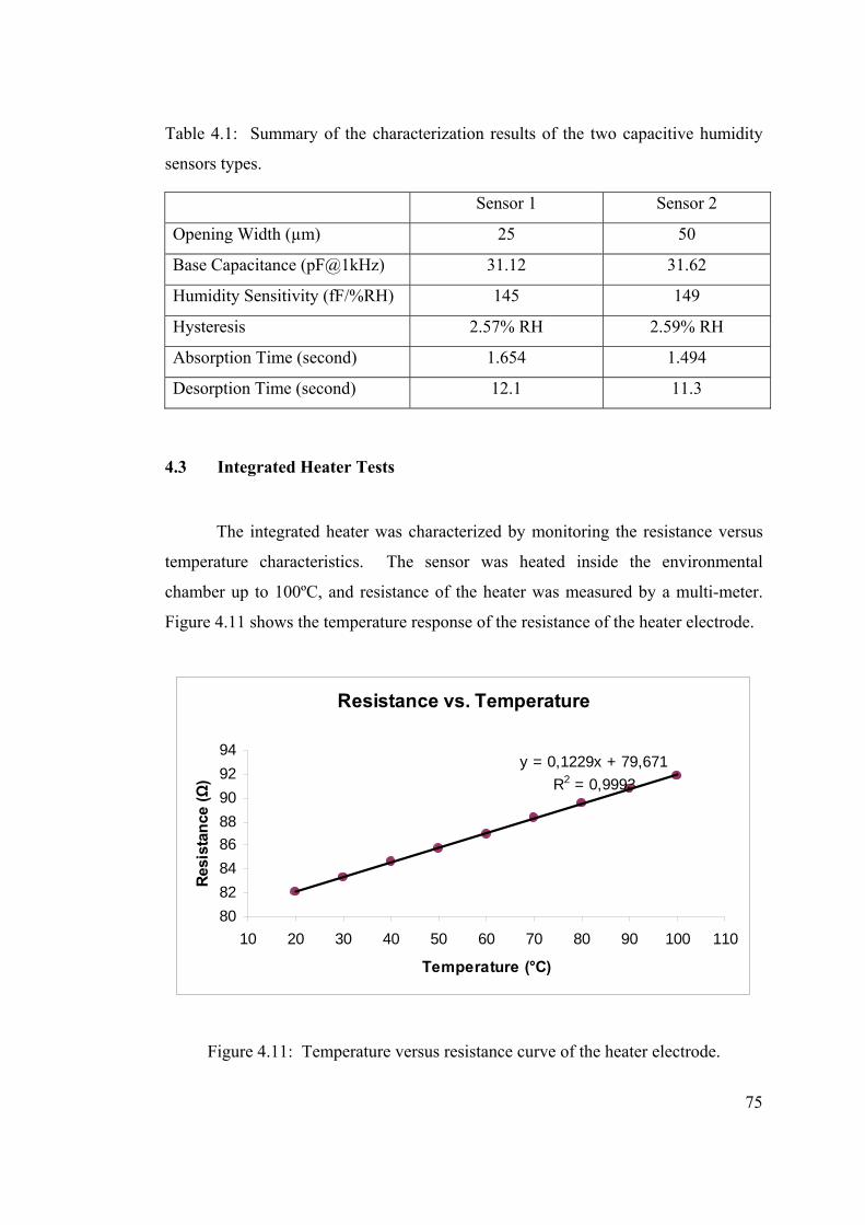
75
Table 4.1: Summary of the characterization results of the two capacitive humidity
sensors types.
Sensor 1 Sensor 2
Opening Width (µm) 25 50
Base Capacitance (pF@1kHz) 31.12 31.62
Humidity Sensitivity (fF/%RH) 145 149
Hysteresis 2.57% RH 2.59% RH
Absorption Time (second) 1.654 1.494
Desorption Time (second) 12.1 11.3
4.3 Integrated Heater Tests
The integrated heater was characterized by monitoring the resistance versus
temperature characteristics. The sensor was heated inside the environmental
chamber up to 100ºC, and resistance of the heater was measured by a multi-meter.
Figure 4.11 shows the temperature response of the resistance of the heater electrode.
Resistance vs. Temperature
y = 0,1229x + 79,671R2 = 0,9993
8082848688909294
10 20 30 40 50 60 70 80 90 100 110
Temperature (°C)
Resi
stan
ce (Ω
)
Figure 4.11: Temperature versus resistance curve of the heater electrode.
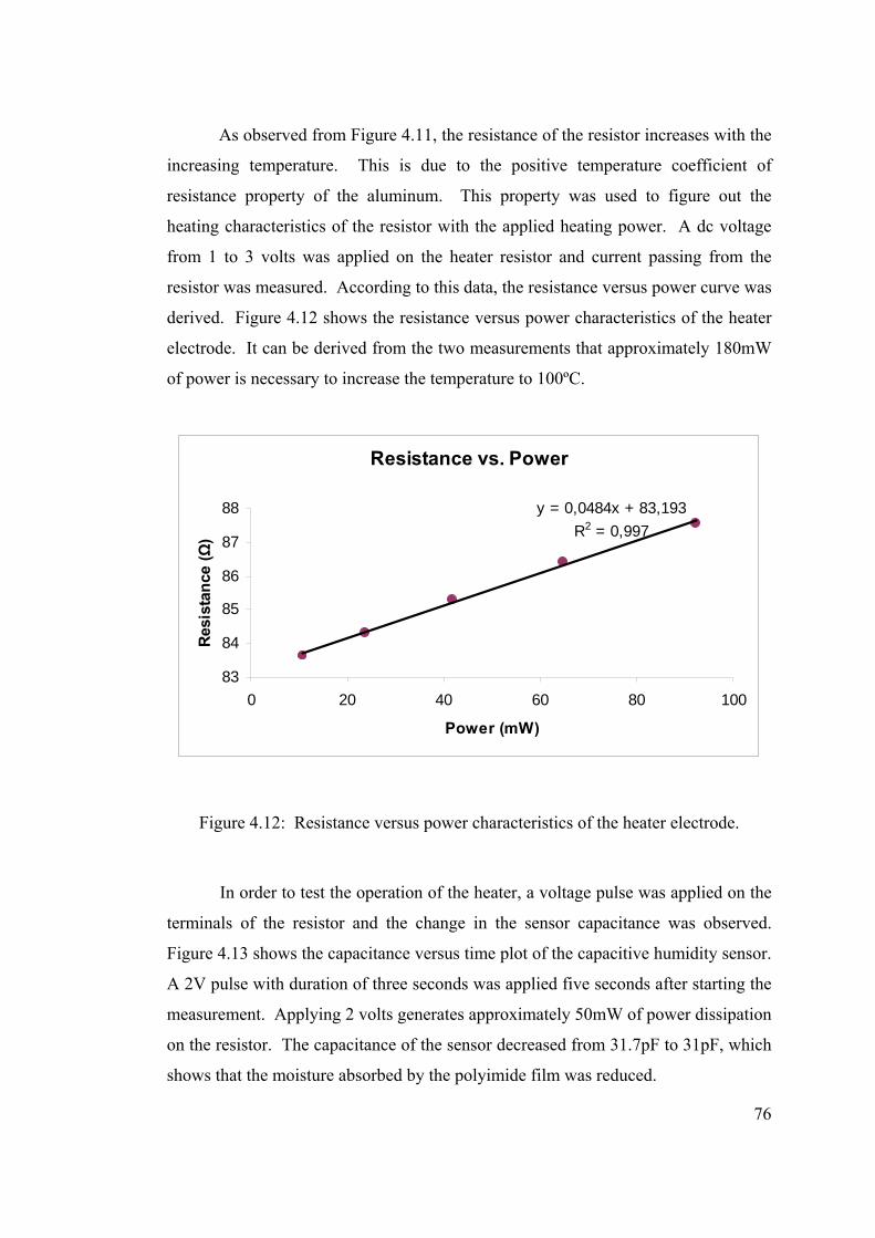
76
As observed from Figure 4.11, the resistance of the resistor increases with the
increasing temperature. This is due to the positive temperature coefficient of
resistance property of the aluminum. This property was used to figure out the
heating characteristics of the resistor with the applied heating power. A dc voltage
from 1 to 3 volts was applied on the heater resistor and current passing from the
resistor was measured. According to this data, the resistance versus power curve was
derived. Figure 4.12 shows the resistance versus power characteristics of the heater
electrode. It can be derived from the two measurements that approximately 180mW
of power is necessary to increase the temperature to 100ºC.
Resistance vs. Power
y = 0,0484x + 83,193R2 = 0,997
83
84
85
86
87
88
0 20 40 60 80 100
Power (mW)
Res
ista
nce
(Ω)
Figure 4.12: Resistance versus power characteristics of the heater electrode.
In order to test the operation of the heater, a voltage pulse was applied on the
terminals of the resistor and the change in the sensor capacitance was observed.
Figure 4.13 shows the capacitance versus time plot of the capacitive humidity sensor.
A 2V pulse with duration of three seconds was applied five seconds after starting the
measurement. Applying 2 volts generates approximately 50mW of power dissipation
on the resistor. The capacitance of the sensor decreased from 31.7pF to 31pF, which
shows that the moisture absorbed by the polyimide film was reduced.
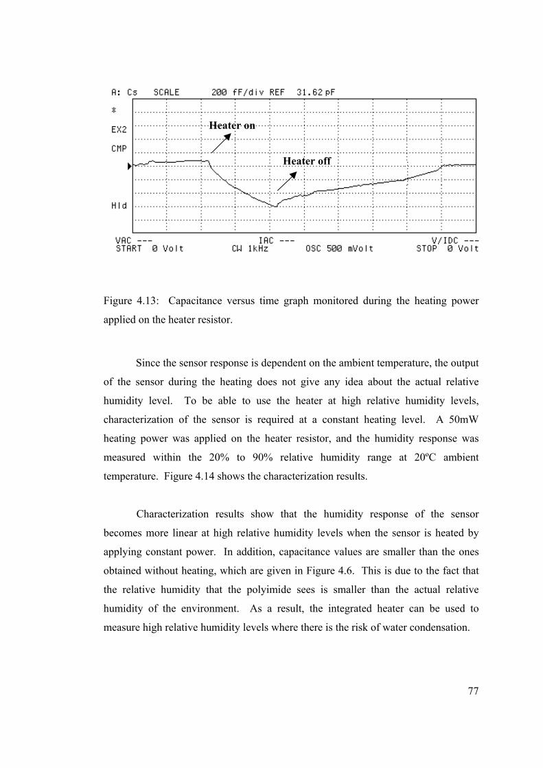
77
Figure 4.13: Capacitance versus time graph monitored during the heating power
applied on the heater resistor.
Since the sensor response is dependent on the ambient temperature, the output
of the sensor during the heating does not give any idea about the actual relative
humidity level. To be able to use the heater at high relative humidity levels,
characterization of the sensor is required at a constant heating level. A 50mW
heating power was applied on the heater resistor, and the humidity response was
measured within the 20% to 90% relative humidity range at 20ºC ambient
temperature. Figure 4.14 shows the characterization results.
Characterization results show that the humidity response of the sensor
becomes more linear at high relative humidity levels when the sensor is heated by
applying constant power. In addition, capacitance values are smaller than the ones
obtained without heating, which are given in Figure 4.6. This is due to the fact that
the relative humidity that the polyimide sees is smaller than the actual relative
humidity of the environment. As a result, the integrated heater can be used to
measure high relative humidity levels where there is the risk of water condensation.
Heater on
Heater off
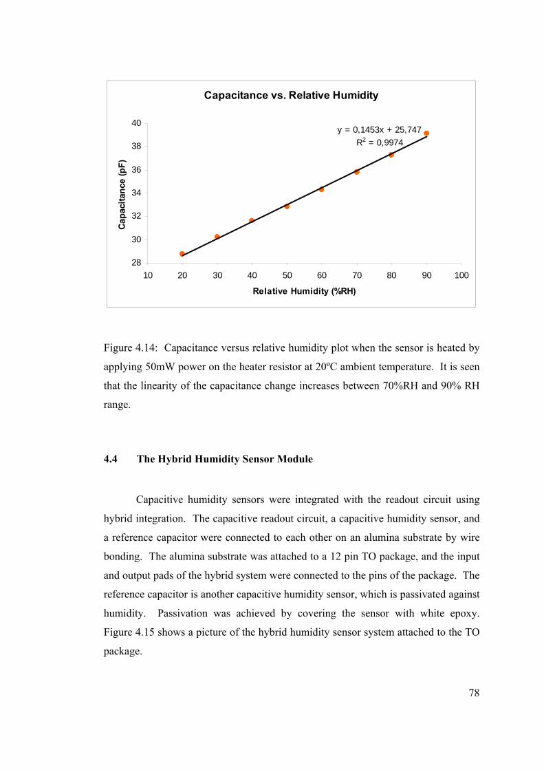
78
Capacitance vs. Relative Humidity
y = 0,1453x + 25,747R2 = 0,9974
28
30
32
34
36
38
40
10 20 30 40 50 60 70 80 90 100
Relative Humidity (%RH)
Capa
cita
nce
(pF)
Figure 4.14: Capacitance versus relative humidity plot when the sensor is heated by
applying 50mW power on the heater resistor at 20ºC ambient temperature. It is seen
that the linearity of the capacitance change increases between 70%RH and 90% RH
range.
4.4 The Hybrid Humidity Sensor Module
Capacitive humidity sensors were integrated with the readout circuit using
hybrid integration. The capacitive readout circuit, a capacitive humidity sensor, and
a reference capacitor were connected to each other on an alumina substrate by wire
bonding. The alumina substrate was attached to a 12 pin TO package, and the input
and output pads of the hybrid system were connected to the pins of the package. The
reference capacitor is another capacitive humidity sensor, which is passivated against
humidity. Passivation was achieved by covering the sensor with white epoxy.
Figure 4.15 shows a picture of the hybrid humidity sensor system attached to the TO
package.
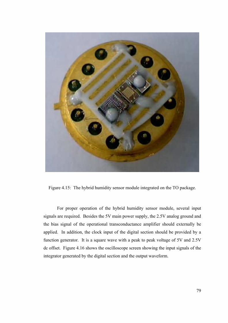
79
Figure 4.15: The hybrid humidity sensor module integrated on the TO package.
For proper operation of the hybrid humidity sensor module, several input
signals are required. Besides the 5V main power supply, the 2.5V analog ground and
the bias signal of the operational transconductance amplifier should externally be
applied. In addition, the clock input of the digital section should be provided by a
function generator. It is a square wave with a peak to peak voltage of 5V and 2.5V
dc offset. Figure 4.16 shows the oscilloscope screen showing the input signals of the
integrator generated by the digital section and the output waveform.
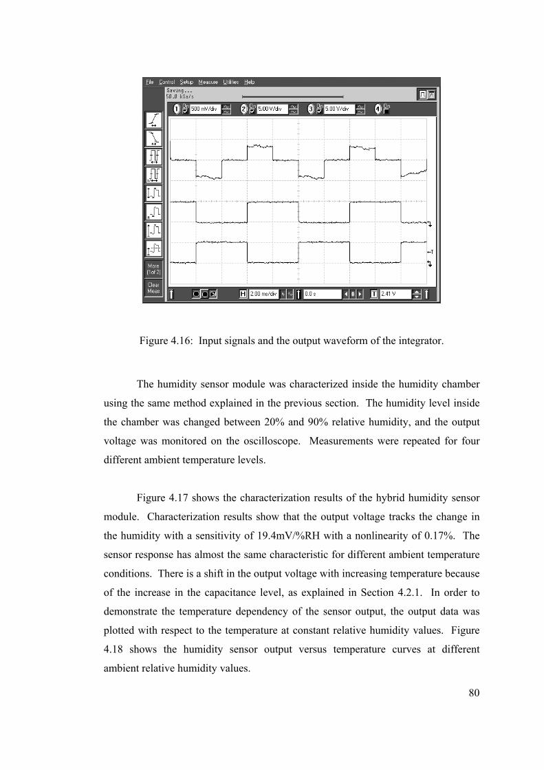
80
Figure 4.16: Input signals and the output waveform of the integrator.
The humidity sensor module was characterized inside the humidity chamber
using the same method explained in the previous section. The humidity level inside
the chamber was changed between 20% and 90% relative humidity, and the output
voltage was monitored on the oscilloscope. Measurements were repeated for four
different ambient temperature levels.
Figure 4.17 shows the characterization results of the hybrid humidity sensor
module. Characterization results show that the output voltage tracks the change in
the humidity with a sensitivity of 19.4mV/%RH with a nonlinearity of 0.17%. The
sensor response has almost the same characteristic for different ambient temperature
conditions. There is a shift in the output voltage with increasing temperature because
of the increase in the capacitance level, as explained in Section 4.2.1. In order to
demonstrate the temperature dependency of the sensor output, the output data was
plotted with respect to the temperature at constant relative humidity values. Figure
4.18 shows the humidity sensor output versus temperature curves at different
ambient relative humidity values.
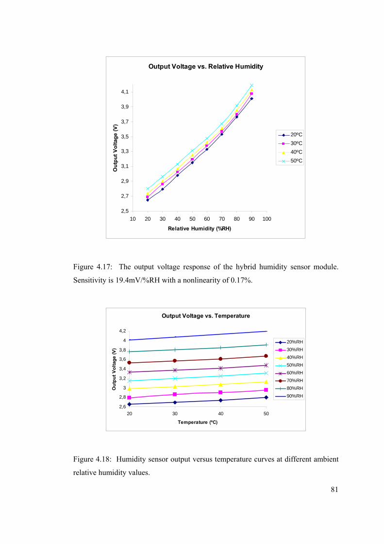
81
Output Voltage vs. Relative Humidity
2,5
2,7
2,9
3,1
3,3
3,5
3,7
3,9
4,1
10 20 30 40 50 60 70 80 90 100
Relative Humidity (%RH)
Out
put V
olta
ge (V
)
20ºC30ºC40ºC50ºC
Figure 4.17: The output voltage response of the hybrid humidity sensor module.
Sensitivity is 19.4mV/%RH with a nonlinearity of 0.17%.
Output Voltage vs. Temperature
2,6
2,8
3
3,2
3,4
3,6
3,8
4
4,2
20 30 40 50
Temperature (ºC)
Out
put V
olta
ge (V
)
20%RH30%RH40%RH50%RH60%RH70%RH80%RH90%RH
Figure 4.18: Humidity sensor output versus temperature curves at different ambient
relative humidity values.
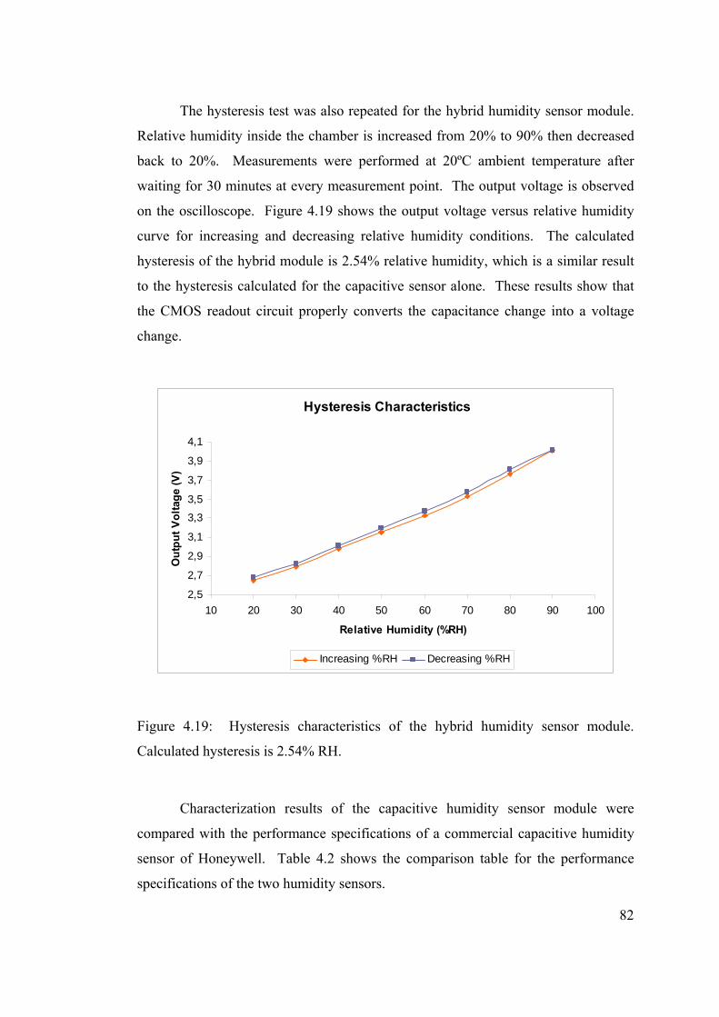
82
The hysteresis test was also repeated for the hybrid humidity sensor module.
Relative humidity inside the chamber is increased from 20% to 90% then decreased
back to 20%. Measurements were performed at 20ºC ambient temperature after
waiting for 30 minutes at every measurement point. The output voltage is observed
on the oscilloscope. Figure 4.19 shows the output voltage versus relative humidity
curve for increasing and decreasing relative humidity conditions. The calculated
hysteresis of the hybrid module is 2.54% relative humidity, which is a similar result
to the hysteresis calculated for the capacitive sensor alone. These results show that
the CMOS readout circuit properly converts the capacitance change into a voltage
change.
Hysteresis Characteristics
2,5
2,7
2,9
3,1
3,3
3,5
3,7
3,9
4,1
10 20 30 40 50 60 70 80 90 100
Relative Humidity (%RH)
Out
put V
olta
ge (V
)
Increasing %RH Decreasing %RH
Figure 4.19: Hysteresis characteristics of the hybrid humidity sensor module.
Calculated hysteresis is 2.54% RH.
Characterization results of the capacitive humidity sensor module were
compared with the performance specifications of a commercial capacitive humidity
sensor of Honeywell. Table 4.2 shows the comparison table for the performance
specifications of the two humidity sensors.
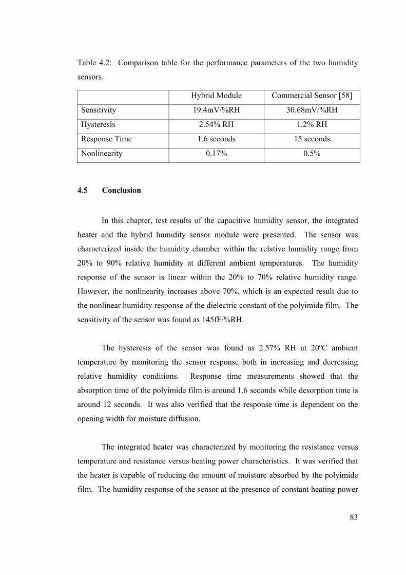
83
Table 4.2: Comparison table for the performance parameters of the two humidity
sensors.
Hybrid Module Commercial Sensor [58]
Sensitivity 19.4mV/%RH 30.68mV/%RH
Hysteresis 2.54% RH 1.2% RH
Response Time 1.6 seconds 15 seconds
Nonlinearity 0.17% 0.5%
4.5 Conclusion
In this chapter, test results of the capacitive humidity sensor, the integrated
heater and the hybrid humidity sensor module were presented. The sensor was
characterized inside the humidity chamber within the relative humidity range from
20% to 90% relative humidity at different ambient temperatures. The humidity
response of the sensor is linear within the 20% to 70% relative humidity range.
However, the nonlinearity increases above 70%, which is an expected result due to
the nonlinear humidity response of the dielectric constant of the polyimide film. The
sensitivity of the sensor was found as 145fF/%RH.
The hysteresis of the sensor was found as 2.57% RH at 20ºC ambient
temperature by monitoring the sensor response both in increasing and decreasing
relative humidity conditions. Response time measurements showed that the
absorption time of the polyimide film is around 1.6 seconds while desorption time is
around 12 seconds. It was also verified that the response time is dependent on the
opening width for moisture diffusion.
The integrated heater was characterized by monitoring the resistance versus
temperature and resistance versus heating power characteristics. It was verified that
the heater is capable of reducing the amount of moisture absorbed by the polyimide
film. The humidity response of the sensor at the presence of constant heating power
84
was also measured. In addition, it was found out that approximately 180mW of
power is necessary to increase the temperature to 100ºC.
Characterization tests were repeated on the hybrid humidity sensor module.
The hybrid module showed a humidity sensitivity of 19.4mV/%RH with a
nonlinearity of 0.17%. The hysteresis of the hybrid module is almost the same as the
hysteresis of the capacitive sensor. In addition, the sensor is capable of measuring
less than 3% change in the relative humidity.
85
5. CHAPTER 5
A THERMAL CONDUCTIVITY BASED HUMIDITY SENSOR
IN A STANDART CMOS PROCESS
This chapter presents the design and implementation of a thermal
conductivity based humidity sensor integrated with the readout circuit using standard
CMOS fabrication. Section 5.1 explains the theory of humidity sensing using
thermal conductivity of the air and the water vapor. Section 5.2 describes the sensor
design and discusses the importance of some structural parameters in the
performance of the sensor. This section also gives information about the thermal
properties and the temperature sensitivity of the diodes, which are used as sensing
elements in the sensor. Section 5.3 explains the readout circuit of the sensor and
demonstrates the chip layout. Sections 5.4 and 5.5 discuss the post processing of the
chip and the test results respectively.
5.1 Humidity Sensing Principle
The humidity sensor designed in this study uses a similar approach to the
thermal conductivity based humidity sensors described in Section 1.3.5. In this
humidity sensing method, the difference between the thermal conductivities of air
and water vapor is used. Thermal conductivities of air and water vapor are both
increasing functions of temperature, but the thermal conductivity of water vapor
exceeds the thermal conductivity of air at high temperatures. Figure 5.1 shows the
thermal conductivity versus temperature plots for air and water vapor [59].
CHAPTER 5
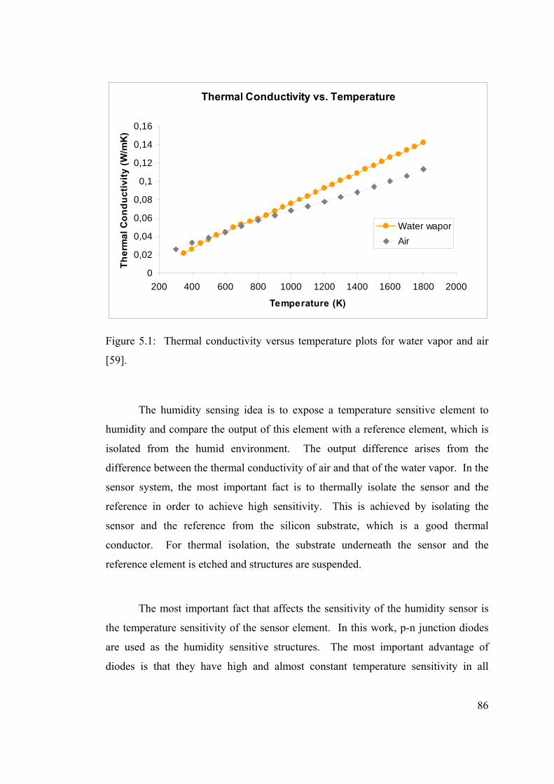
86
Thermal Conductivity vs. Temperature
0
0,02
0,04
0,06
0,08
0,1
0,12
0,14
0,16
200 400 600 800 1000 1200 1400 1600 1800 2000
Temperature (K)
Ther
mal
Con
duct
ivity
(W/m
K)
Water waporAir
Figure 5.1: Thermal conductivity versus temperature plots for water vapor and air
[59].
The humidity sensing idea is to expose a temperature sensitive element to
humidity and compare the output of this element with a reference element, which is
isolated from the humid environment. The output difference arises from the
difference between the thermal conductivity of air and that of the water vapor. In the
sensor system, the most important fact is to thermally isolate the sensor and the
reference in order to achieve high sensitivity. This is achieved by isolating the
sensor and the reference from the silicon substrate, which is a good thermal
conductor. For thermal isolation, the substrate underneath the sensor and the
reference element is etched and structures are suspended.
The most important fact that affects the sensitivity of the humidity sensor is
the temperature sensitivity of the sensor element. In this work, p-n junction diodes
are used as the humidity sensitive structures. The most important advantage of
diodes is that they have high and almost constant temperature sensitivity in all
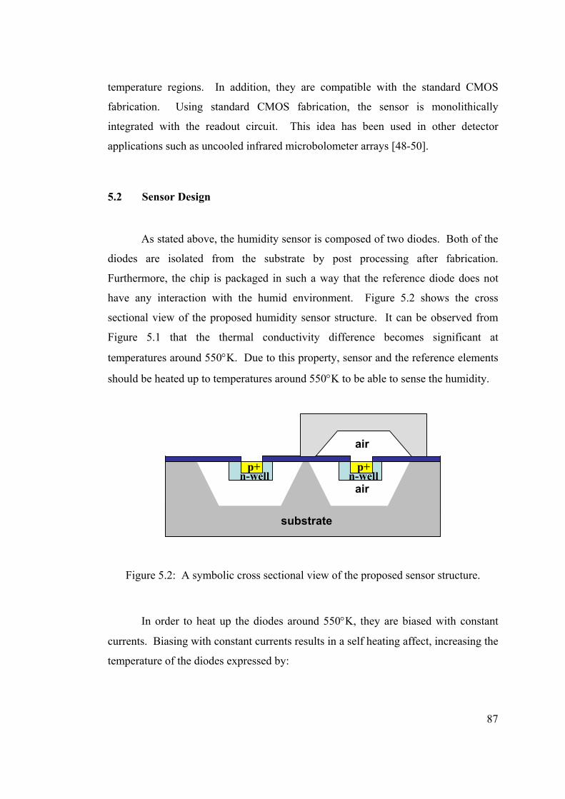
87
temperature regions. In addition, they are compatible with the standard CMOS
fabrication. Using standard CMOS fabrication, the sensor is monolithically
integrated with the readout circuit. This idea has been used in other detector
applications such as uncooled infrared microbolometer arrays [48-50].
5.2 Sensor Design
As stated above, the humidity sensor is composed of two diodes. Both of the
diodes are isolated from the substrate by post processing after fabrication.
Furthermore, the chip is packaged in such a way that the reference diode does not
have any interaction with the humid environment. Figure 5.2 shows the cross
sectional view of the proposed humidity sensor structure. It can be observed from
Figure 5.1 that the thermal conductivity difference becomes significant at
temperatures around 550°K. Due to this property, sensor and the reference elements
should be heated up to temperatures around 550°K to be able to sense the humidity.
Figure 5.2: A symbolic cross sectional view of the proposed sensor structure.
In order to heat up the diodes around 550°K, they are biased with constant
currents. Biasing with constant currents results in a self heating affect, increasing the
temperature of the diodes expressed by:
substrate
air
air
p+p+n-well n-well
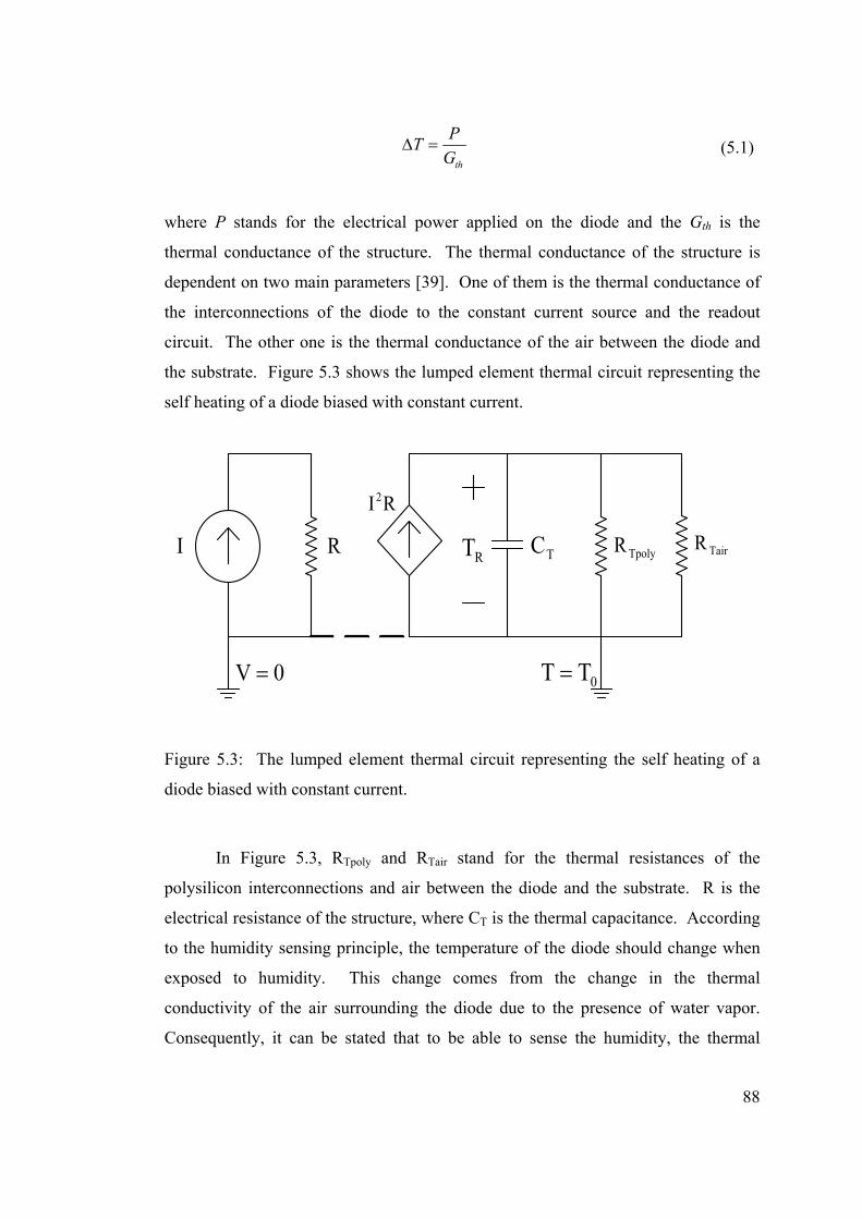
88
th
PTG
∆ = (5.1)
where P stands for the electrical power applied on the diode and the Gth is the
thermal conductance of the structure. The thermal conductance of the structure is
dependent on two main parameters [39]. One of them is the thermal conductance of
the interconnections of the diode to the constant current source and the readout
circuit. The other one is the thermal conductance of the air between the diode and
the substrate. Figure 5.3 shows the lumped element thermal circuit representing the
self heating of a diode biased with constant current.
RI
RI2
TpolyRTC
0V = 0TT =
RT TairR
Figure 5.3: The lumped element thermal circuit representing the self heating of a
diode biased with constant current.
In Figure 5.3, RTpoly and RTair stand for the thermal resistances of the
polysilicon interconnections and air between the diode and the substrate. R is the
electrical resistance of the structure, where CT is the thermal capacitance. According
to the humidity sensing principle, the temperature of the diode should change when
exposed to humidity. This change comes from the change in the thermal
conductivity of the air surrounding the diode due to the presence of water vapor.
Consequently, it can be stated that to be able to sense the humidity, the thermal
89
conductance of air should be larger than the thermal conductance of the
interconnections of the diode. In other words, the thermal conductance of the
interconnection should be as small as possible in order to increase the humidity
sensitivity. Furthermore, it can be concluded from Equation 5.1 that, if the thermal
conductance is low, it is possible to heat up the diodes to high temperatures with less
power.
5.2.1 Temperature Sensitivity of Diodes
Temperature sensitivity of the semiconductor diodes can be derived
considering the ideal diode equation as follows [51]. In the ideal diode equation, the
diode current is given by:
/( -1)TV V
sI I e= (5.2)
where Is is the saturation current of the diode, V is the diode voltage, and VT is the
thermal voltage. The ideal diode equation is affected by the temperature in two
ways. First of all, the saturation current is dependent on the intrinsic carrier
concentration, which is a function of temperature. Secondly, the thermal voltage is
linearly dependent on the temperature. The effect of temperature on Is is a result of
the temperature dependence of the square of the intrinsic carrier concentration:
- /2 3( ) go TV V
in T KT e= (5.3)
where Vgo is the bang-gap voltage. The fractional change in Is per unit change in
temperature is approximately equal to the fractional change in ni2 per unit change in
temperature.
2
2
1 1s i
s i
dI dnI dT n dT
= (5.4)
90
1 3 1 gos
s T
VdII dT T T V
= + (5.5)
Near the room temperature, the first term is approximately 1%/K, and the second
term is 14%/K. Finally, the temperature dependence of the diode voltage at a fixed
current is expressed as:
0
[ ln( / )]T s
dI
d V I IdVdT dT=
=
(5.6)
0
1- sT
dI s
dIdV V VdT T I dT=
⎛ ⎞= ⎜ ⎟
⎝ ⎠ (5.7)
At a constant forward current, the temperature coefficient of a silicon p-n
junction diode is approximately -2mV/ºC. Furthermore, temperature sensitivity of
the diode is almost constant in a wide temperature range.
5.2.2 Humidity Sensitive Diode Design
In the diode design, the most important design goal is to decrease the thermal
conductance of the diode interconnections in order to increase the sensitivity of the
sensor. As given in Section 2.3, the thermal conductance of a rectangular shaped
resistor is given by:
thAGl
σ= (5.8)
where σ is the thermal conductivity, A is the cross sectional area, and l is the length
of the resistor.
91
The humidity sensitive diode design was performed in a 0.6µm CMOS
process. In this process, two metal and two poly-silicon layers are available for
interconnection. Metal layers, having high thermal conductivity values, are not
suitable for usage as interconnect layers. Polysilicon has a relatively low thermal
conductivity, which can provide a low thermal conductance if it is used as the
interconnect layer. However, it has a high resistivity, which is an important
disadvantage for the temperature sensing applications. This disadvantage arises from
the fact that the resistance is a function of temperature. The effect of temperature on
the resistance is expressed as:
(1 )oR R Tα= + ∆ (5.9)
where α is called the temperature coefficient of resistance (TCR), Ro is the initial
resistance and ∆T is the temperature variation. The TCR of polysilicon is a positive
value, which results in a positive temperature sensitivity of the resistor. As
expressed in the previous subsection, the temperature sensitivity of the diode is
negative. Consequently, positive temperature sensitivity of a resistor reduces the
overall sensitivity of the structure. This phenomenon can be shown mathematically
as follows. Since the diode is biased with a constant current, the output voltage is
expressed as:
d polyV V iR= + (5.10)
Temperature sensitivity of the output voltage is found by inserting equation 5.9 into
equation 5.10 and taking the derivative of both sides with respect to temperature:
ddVdV iRdT dT
α= + (5.11)
It should be mentioned that the dVd/dT term has a negative value, while the αiR term
has a positive value; therefore, it reduces the sensitivity provided by the diode. The
92
αiR term is directly proportional to the bias current, the resistance and the TCR of the
interconnect layer. In order to increase the sensitivity of the sensor, either the bias
current or the resistance should be decreased. The resistance can be decreased by
either decreasing the length or increasing the cross sectional area of the resistor. It
should be noted that this operation increases the thermal conductance of the
structure, which is an unwanted result. On the other hand, decreasing the current
reduces the power dissipated on the resistor, so the final temperature of the device.
However, the sensor should be heated up to a proper temperature level to be able to
sense the humidity. In conclusion, there is a compromise between the bias current,
the resistance, and the thermal conductance of the diode structure in terms of their
effect on the performance of the sensor. In order to find an optimum bias level and a
resistor dimension, MATLAB simulations were performed. The total pixel area was
also fixed to a value which guarantees the etching of the silicon substrate during the
post-CMOS process. The temperature sensitivity of the diode and the final
temperature were plotted with respect to the polysilicon length to width ratio and the
bias current.
Figure 5.4 shows the simulation results. As stated above, the diodes should
be heated up to approximately 250ºC to be able to sense the humidity. Simulation
results show that the final temperature increases and sensitivity of the sensor
decreases with the increasing bias current and the length over width ratio.
Consequently, the optimum design can be achieved by taking the values around the
250ºC final temperature level. The length over width ratio was selected as 140,
which is the most suitable value for the post processing of the diode. The sensitivity,
sensitivity over power dissipation, and the operating temperature curves were plotted
with respect to the bias current. Figure 5.5 shows the simulation results.
As observed from Figure 5.5, the bias current of the diode should be larger
than 100µA to be able to heat up the diodes to the desired temperature levels. Since
the sensitivity is decreasing with the increasing bias current, minimum possible bias
current is selected, which is 100µA.
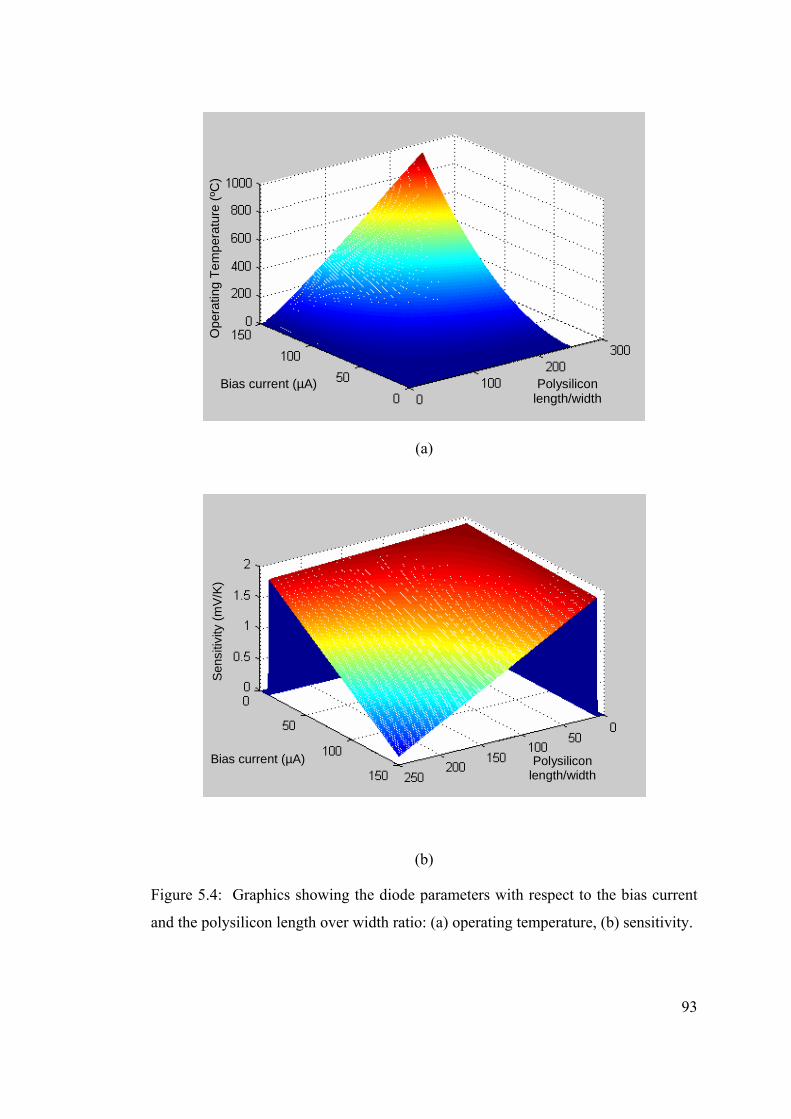
93
Bias current (µA) Polysilicon length/width
Ope
ratin
g Te
mpe
ratu
re (º
C)
(a)
Polysilicon length/width
Bias current (µA)
Sens
itivi
ty (m
V/K)
(b)
Figure 5.4: Graphics showing the diode parameters with respect to the bias current
and the polysilicon length over width ratio: (a) operating temperature, (b) sensitivity.
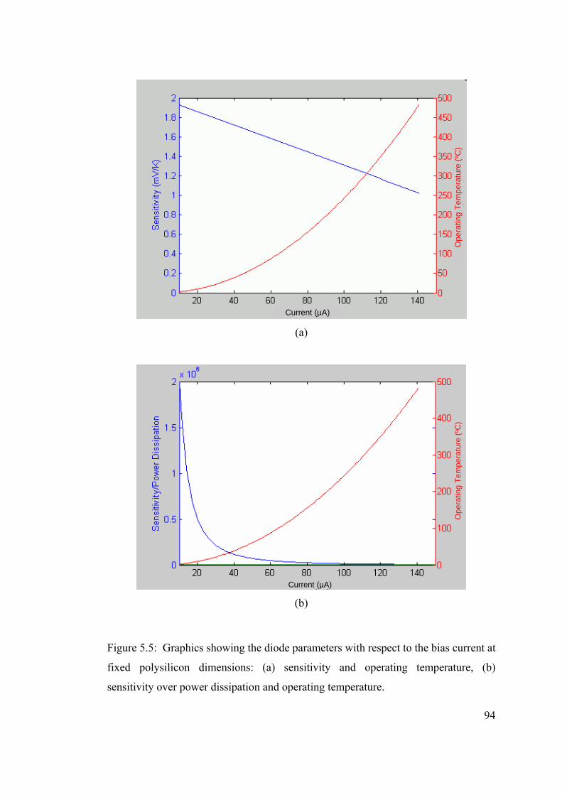
94
Ope
ratin
g Te
mpe
ratu
re (º
C)
Current (µA) (a)
Current (µA)
Ope
ratin
g Te
mpe
ratu
re (º
C)
(b)
Figure 5.5: Graphics showing the diode parameters with respect to the bias current at
fixed polysilicon dimensions: (a) sensitivity and operating temperature, (b)
sensitivity over power dissipation and operating temperature.
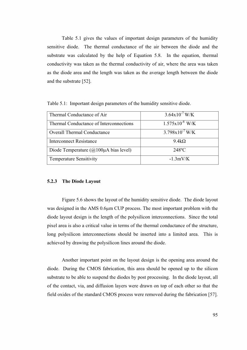
95
Table 5.1 gives the values of important design parameters of the humidity
sensitive diode. The thermal conductance of the air between the diode and the
substrate was calculated by the help of Equation 5.8. In the equation, thermal
conductivity was taken as the thermal conductivity of air, where the area was taken
as the diode area and the length was taken as the average length between the diode
and the substrate [52].
Table 5.1: Important design parameters of the humidity sensitive diode.
Thermal Conductance of Air 3.64x10⁻⁷ W/K
Thermal Conductance of Interconnections 1.575x10⁻⁸ W/K
Overall Thermal Conductance 3.798x10⁻⁷ W/K
Interconnect Resistance 9.4kΩ
Diode Temperature (@100µA bias level) 248ºC
Temperature Sensitivity -1.3mV/K
5.2.3 The Diode Layout
Figure 5.6 shows the layout of the humidity sensitive diode. The diode layout
was designed in the AMS 0.6µm CUP process. The most important problem with the
diode layout design is the length of the polysilicon interconnections. Since the total
pixel area is also a critical value in terms of the thermal conductance of the structure,
long polysilicon interconnections should be inserted into a limited area. This is
achieved by drawing the polysilicon lines around the diode.
Another important point on the layout design is the opening area around the
diode. During the CMOS fabrication, this area should be opened up to the silicon
substrate to be able to suspend the diodes by post processing. In the diode layout, all
of the contact, via, and diffusion layers were drawn on top of each other so that the
field oxides of the standard CMOS process were removed during the fabrication [57].
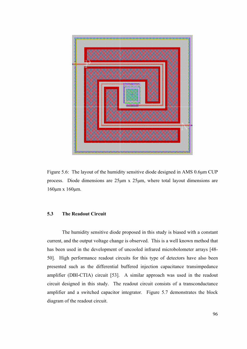
96
Figure 5.6: The layout of the humidity sensitive diode designed in AMS 0.6µm CUP
process. Diode dimensions are 25µm x 25µm, where total layout dimensions are
160µm x 160µm.
5.3 The Readout Circuit
The humidity sensitive diode proposed in this study is biased with a constant
current, and the output voltage change is observed. This is a well known method that
has been used in the development of uncooled infrared microbolometer arrays [48-
50]. High performance readout circuits for this type of detectors have also been
presented such as the differential buffered injection capacitance transimpedance
amplifier (DBI-CTIA) circuit [53]. A similar approach was used in the readout
circuit designed in this study. The readout circuit consists of a transconductance
amplifier and a switched capacitor integrator. Figure 5.7 demonstrates the block
diagram of the readout circuit.
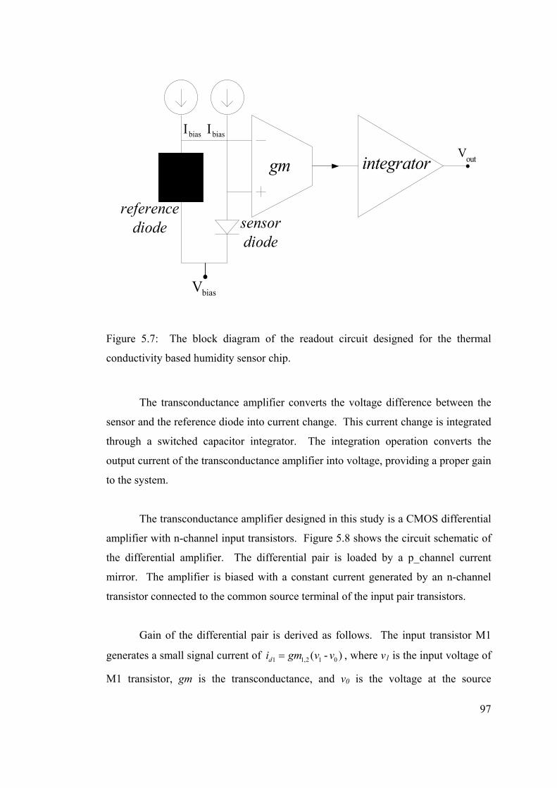
97
gmVout
biasV
biasI biasI
integrator
sensordiode
referencediode
Figure 5.7: The block diagram of the readout circuit designed for the thermal
conductivity based humidity sensor chip.
The transconductance amplifier converts the voltage difference between the
sensor and the reference diode into current change. This current change is integrated
through a switched capacitor integrator. The integration operation converts the
output current of the transconductance amplifier into voltage, providing a proper gain
to the system.
The transconductance amplifier designed in this study is a CMOS differential
amplifier with n-channel input transistors. Figure 5.8 shows the circuit schematic of
the differential amplifier. The differential pair is loaded by a p_channel current
mirror. The amplifier is biased with a constant current generated by an n-channel
transistor connected to the common source terminal of the input pair transistors.
Gain of the differential pair is derived as follows. The input transistor M1
generates a small signal current of 1 1,2 1 0( - )di gm v v= , where v1 is the input voltage of
M1 transistor, gm is the transconductance, and v0 is the voltage at the source
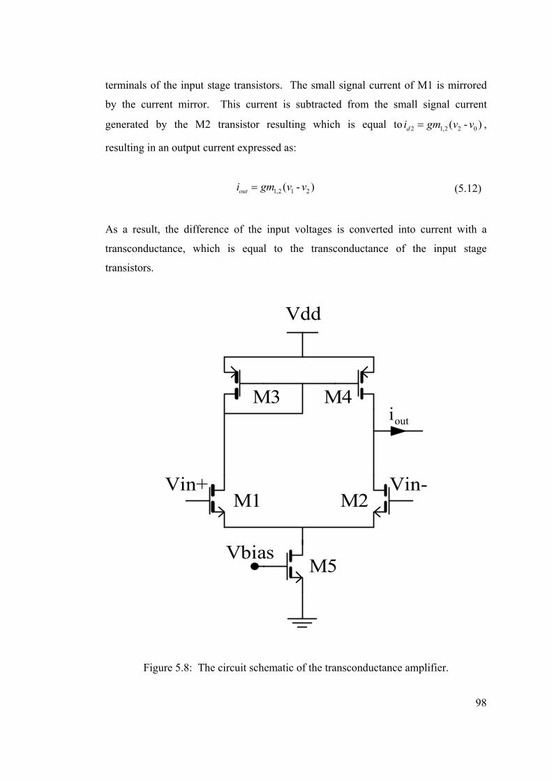
98
terminals of the input stage transistors. The small signal current of M1 is mirrored
by the current mirror. This current is subtracted from the small signal current
generated by the M2 transistor resulting which is equal to 2 1,2 2 0( - )di gm v v= ,
resulting in an output current expressed as:
1,2 1 2( - )outi gm v v= (5.12)
As a result, the difference of the input voltages is converted into current with a
transconductance, which is equal to the transconductance of the input stage
transistors.
Vin+
Vdd
M1 M2
M3 M4
Vin-
M5Vbias
outi
Figure 5.8: The circuit schematic of the transconductance amplifier.
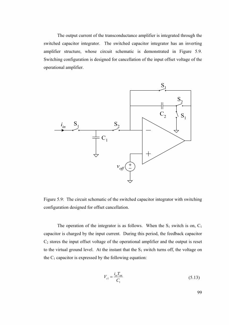
99
The output current of the transconductance amplifier is integrated through the
switched capacitor integrator. The switched capacitor integrator has an inverting
amplifier structure, whose circuit schematic is demonstrated in Figure 5.9.
Switching configuration is designed for cancellation of the input offset voltage of the
operational amplifier.
iin S1
S1
S1
S2
S2
C2
C1
voff
Figure 5.9: The circuit schematic of the switched capacitor integrator with switching
configuration designed for offset cancellation.
The operation of the integrator is as follows. When the S1 switch is on, C1
capacitor is charged by the input current. During this period, the feedback capacitor
C2 stores the input offset voltage of the operational amplifier and the output is reset
to the virtual ground level. At the instant that the S1 switch turns off, the voltage on
the C1 capacitor is expressed by the following equation:
int1
1
inc
i TVC
= (5.13)
100
where Tint is the charging time of the capacitor and iin is the current that charges the
C1 capacitor. When the S2 switch turns on, the charge stored by the C1 capacitor is
injected to the C2 capacitor. The output voltage of the integrator at this state is given
by:
11
2
-out CCV VC
= (5.14)
At this state, the offset voltage stored on the C2 capacitor is also subtracted from the
output voltage. It should be noted that the iin parameter of Equation 5.13 is the
output current of the transconductance amplifier given by Equation 5.12. In order to
find the gain of the overall system, Equations 5.12 and 5.13 are inserted into
Equation 5.14. Gain is expressed by the ratio of the output voltage to the differential
input voltage, which is equal to:
1,2 int
2
out
in
gm TVV C
= (5.15)
It should be noted that the integration operation is performed on the C1
capacitor, so value of the C1 capacitor is also important although it is not present at
the output expression. In fact, the gain of the system is determined by the C1
capacitor according to Equation 5.13, and then it is scaled by the C2 capacitor.
Figure 5.10 shows the layout of the humidity sensitive diode chip. The layout
of the chip was designed in the AMS 0.6µm CUP process. In the layout design, the
post processing and the packaging of the chip was also considered. The reference
diode was placed in the middle of the die, and it was surrounded by a 250µm wide
metal3 ring. This ring was placed to indicate the area that will be isolated from the
environment. Figure 5.11 shows a schematic view of the complete sensor system.
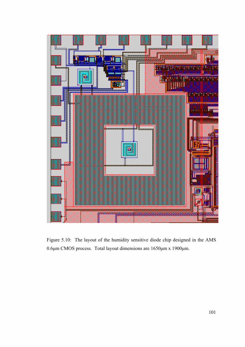
101
Figure 5.10: The layout of the humidity sensitive diode chip designed in the AMS
0.6µm CMOS process. Total layout dimensions are 1650µm x 1900µm.
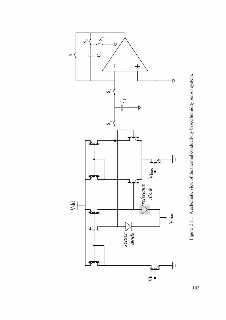
102
S 1
S 1
S 1
S 2
S 2
C 2
C 1
Vdd
Vbias
Vbias
Vbias
refer
ence
diod
e
sens
or di
ode
Figu
re 5
.11:
A sc
hem
atic
vie
w o
f the
ther
mal
con
duct
ivity
bas
ed h
umid
ity se
nsor
syst
em.
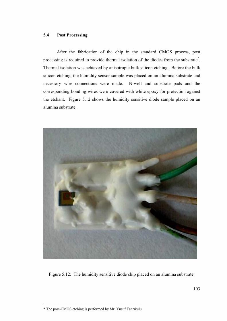
103
5.4 Post Processing
After the fabrication of the chip in the standard CMOS process, post
processing is required to provide thermal isolation of the diodes from the substrate*.
Thermal isolation was achieved by anisotropic bulk silicon etching. Before the bulk
silicon etching, the humidity sensor sample was placed on an alumina substrate and
necessary wire connections were made. N-well and substrate pads and the
corresponding bonding wires were covered with white epoxy for protection against
the etchant. Figure 5.12 shows the humidity sensitive diode sample placed on an
alumina substrate.
Figure 5.12: The humidity sensitive diode chip placed on an alumina substrate.
___________________________________________________
* The post-CMOS etching is performed by Mr. Yusuf Tanrıkulu.
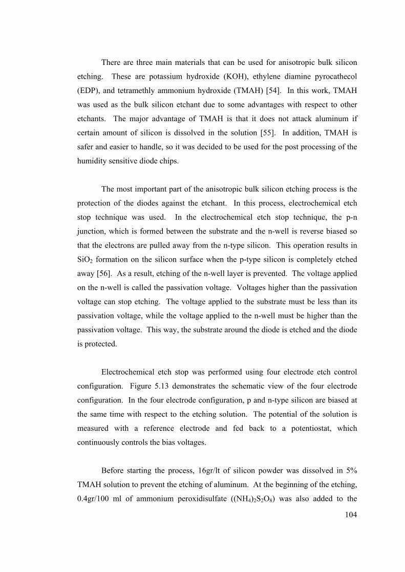
104
There are three main materials that can be used for anisotropic bulk silicon
etching. These are potassium hydroxide (KOH), ethylene diamine pyrocathecol
(EDP), and tetramethly ammonium hydroxide (TMAH) [54]. In this work, TMAH
was used as the bulk silicon etchant due to some advantages with respect to other
etchants. The major advantage of TMAH is that it does not attack aluminum if
certain amount of silicon is dissolved in the solution [55]. In addition, TMAH is
safer and easier to handle, so it was decided to be used for the post processing of the
humidity sensitive diode chips.
The most important part of the anisotropic bulk silicon etching process is the
protection of the diodes against the etchant. In this process, electrochemical etch
stop technique was used. In the electrochemical etch stop technique, the p-n
junction, which is formed between the substrate and the n-well is reverse biased so
that the electrons are pulled away from the n-type silicon. This operation results in
SiO2 formation on the silicon surface when the p-type silicon is completely etched
away [56]. As a result, etching of the n-well layer is prevented. The voltage applied
on the n-well is called the passivation voltage. Voltages higher than the passivation
voltage can stop etching. The voltage applied to the substrate must be less than its
passivation voltage, while the voltage applied to the n-well must be higher than the
passivation voltage. This way, the substrate around the diode is etched and the diode
is protected.
Electrochemical etch stop was performed using four electrode etch control
configuration. Figure 5.13 demonstrates the schematic view of the four electrode
configuration. In the four electrode configuration, p and n-type silicon are biased at
the same time with respect to the etching solution. The potential of the solution is
measured with a reference electrode and fed back to a potentiostat, which
continuously controls the bias voltages.
Before starting the process, 16gr/lt of silicon powder was dissolved in 5%
TMAH solution to prevent the etching of aluminum. At the beginning of the etching,
0.4gr/100 ml of ammonium peroxidisulfate ((NH4)2S2O8) was also added to the
105
etching solution. This material prevents the formation of hillocks on the surface, but
it slows down the etching process [55]. At the beginning of the etching process there
is no need to bias the n-well layer, since the n-well is not directly exposed to the
solution. Furthermore, when the passivation voltage is applied, the etch rate
decreases. Therefore, in order not to decrease the etch rate at the beginning of the
process, n-well was not biased. The time it takes for the solution to reach the n-well
was determined experimentally, and the etch stop potential was applied accordingly.
Table 5.2 gives the important parameters of the etching process.
Potentiostat
p-su
bstr
ate
n-w
ell
Ref
eren
ce E
lect
rode
Pt
TMAH
Figure 5.13: Four-electrode electrochemical etch stop configuration.
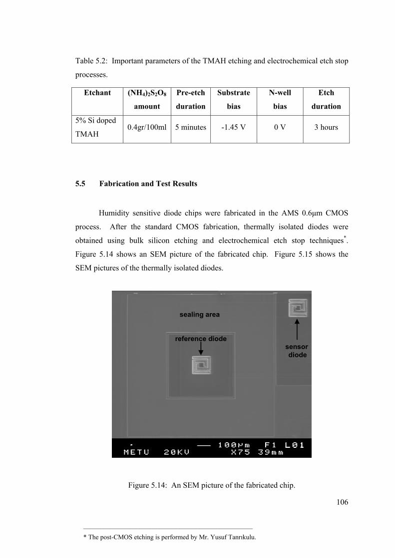
106
Table 5.2: Important parameters of the TMAH etching and electrochemical etch stop
processes.
Etchant (NH4)2S2O8
amount
Pre-etch
duration
Substrate
bias
N-well
bias
Etch
duration
5% Si doped
TMAH 0.4gr/100ml 5 minutes -1.45 V 0 V 3 hours
5.5 Fabrication and Test Results
Humidity sensitive diode chips were fabricated in the AMS 0.6µm CMOS
process. After the standard CMOS fabrication, thermally isolated diodes were
obtained using bulk silicon etching and electrochemical etch stop techniques*.
Figure 5.14 shows an SEM picture of the fabricated chip. Figure 5.15 shows the
SEM pictures of the thermally isolated diodes.
reference diode
sealing area
sensor diode
Figure 5.14: An SEM picture of the fabricated chip.
___________________________________________________
* The post-CMOS etching is performed by Mr. Yusuf Tanrıkulu.
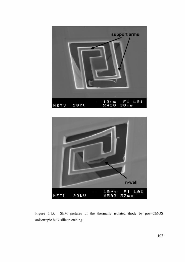
107
support arms
n-well
Figure 5.15: SEM pictures of the thermally isolated diode by post-CMOS
anisotropic bulk silicon etching.
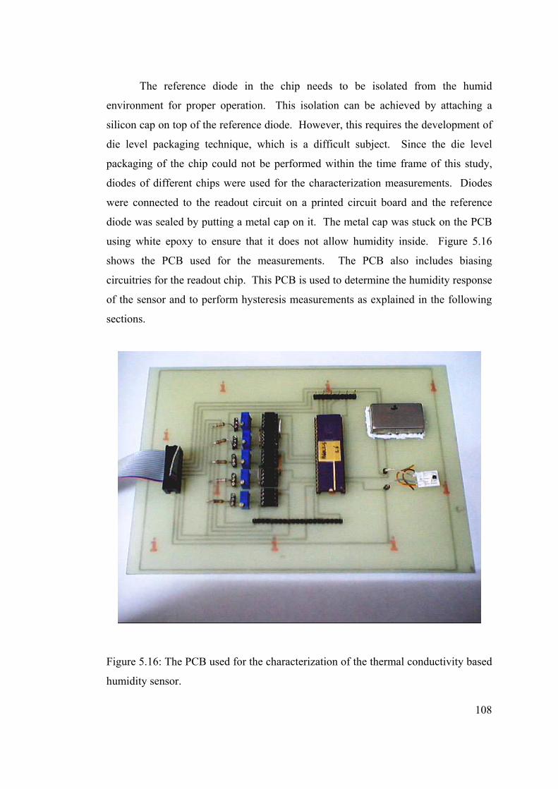
108
The reference diode in the chip needs to be isolated from the humid
environment for proper operation. This isolation can be achieved by attaching a
silicon cap on top of the reference diode. However, this requires the development of
die level packaging technique, which is a difficult subject. Since the die level
packaging of the chip could not be performed within the time frame of this study,
diodes of different chips were used for the characterization measurements. Diodes
were connected to the readout circuit on a printed circuit board and the reference
diode was sealed by putting a metal cap on it. The metal cap was stuck on the PCB
using white epoxy to ensure that it does not allow humidity inside. Figure 5.16
shows the PCB used for the measurements. The PCB also includes biasing
circuitries for the readout chip. This PCB is used to determine the humidity response
of the sensor and to perform hysteresis measurements as explained in the following
sections.
Figure 5.16: The PCB used for the characterization of the thermal conductivity based
humidity sensor.
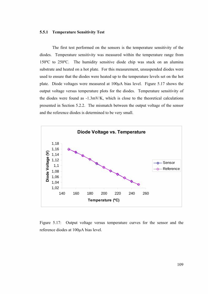
109
5.5.1 Temperature Sensitivity Test
The first test performed on the sensors is the temperature sensitivity of the
diodes. Temperature sensitivity was measured within the temperature range from
150ºC to 250ºC. The humidity sensitive diode chip was stuck on an alumina
substrate and heated on a hot plate. For this measurement, unsuspended diodes were
used to ensure that the diodes were heated up to the temperature levels set on the hot
plate. Diode voltages were measured at 100µA bias level. Figure 5.17 shows the
output voltage versus temperature plots for the diodes. Temperature sensitivity of
the diodes were found as -1.3mV/K, which is close to the theoretical calculations
presented in Section 5.2.2. The mismatch between the output voltage of the sensor
and the reference diodes is determined to be very small.
Diode Voltage vs. Temperature
1,021,041,061,081,1
1,121,141,161,18
140 160 180 200 220 240 260
Temperature (ºC)
Diod
e Vo
ltage
(V)
SensorReference
Figure 5.17: Output voltage versus temperature curves for the sensor and the
reference diodes at 100µA bias level.
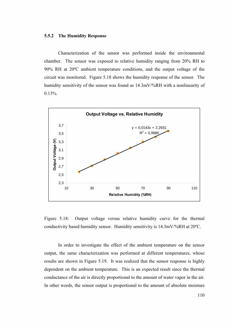
110
5.5.2 The Humidity Response
Characterization of the sensor was performed inside the environmental
chamber. The sensor was exposed to relative humidity ranging from 20% RH to
90% RH at 20ºC ambient temperature conditions, and the output voltage of the
circuit was monitored. Figure 5.18 shows the humidity response of the sensor. The
humidity sensitivity of the sensor was found as 14.3mV/%RH with a nonlinearity of
0.13%.
Output Voltage vs. Relative Humidity
y = 0,0143x + 2,2931R2 = 0,9986
2,3
2,5
2,7
2,9
3,1
3,3
3,5
3,7
10 30 50 70 90 110
Relative Humidity (%RH)
Out
put V
olta
ge (V
)
Figure 5.18: Output voltage versus relative humidity curve for the thermal
conductivity based humidity sensor. Humidity sensitivity is 14.3mV/%RH at 20ºC.
In order to investigate the effect of the ambient temperature on the sensor
output, the same characterization was performed at different temperatures, whose
results are shown in Figure 5.19. It was realized that the sensor response is highly
dependent on the ambient temperature. This is an expected result since the thermal
conductance of the air is directly proportional to the amount of water vapor in the air.
In other words, the sensor output is proportional to the amount of absolute moisture
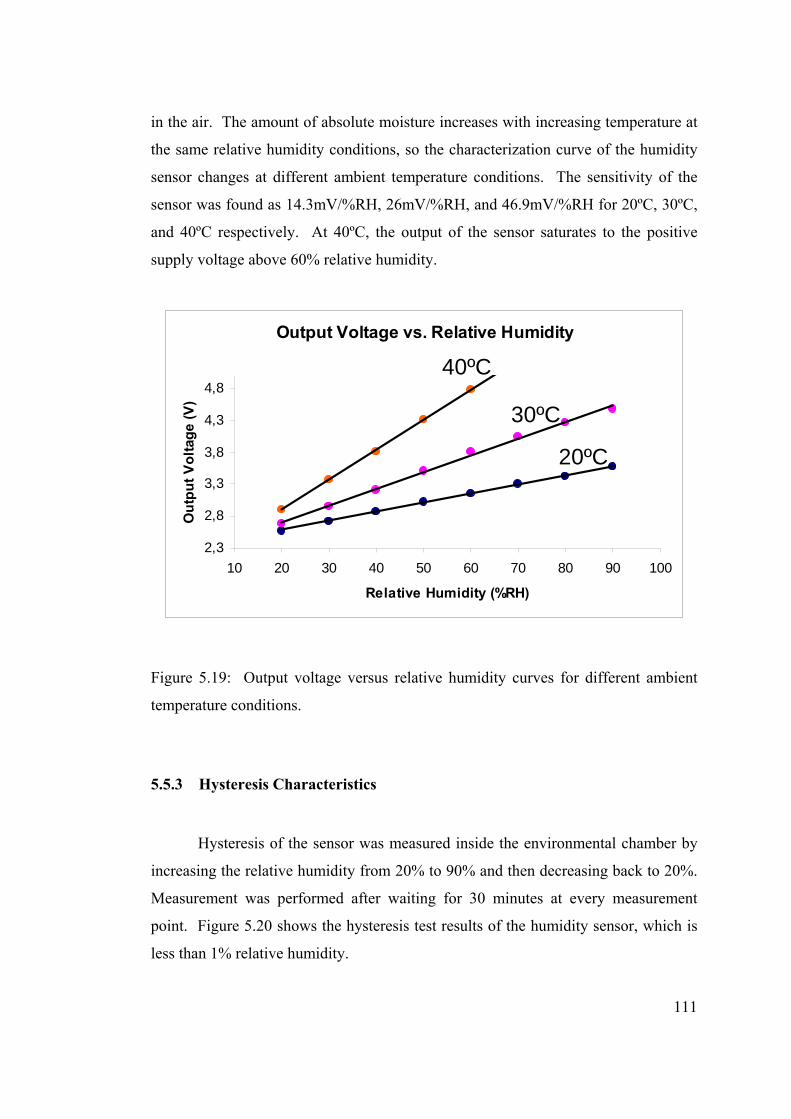
111
in the air. The amount of absolute moisture increases with increasing temperature at
the same relative humidity conditions, so the characterization curve of the humidity
sensor changes at different ambient temperature conditions. The sensitivity of the
sensor was found as 14.3mV/%RH, 26mV/%RH, and 46.9mV/%RH for 20ºC, 30ºC,
and 40ºC respectively. At 40ºC, the output of the sensor saturates to the positive
supply voltage above 60% relative humidity.
Output Voltage vs. Relative Humidity
2,3
2,8
3,3
3,8
4,3
4,8
10 20 30 40 50 60 70 80 90 100
Relative Humidity (%RH)
Out
put V
olta
ge (V
)
40ºC
30ºC
20ºC
Figure 5.19: Output voltage versus relative humidity curves for different ambient
temperature conditions.
5.5.3 Hysteresis Characteristics
Hysteresis of the sensor was measured inside the environmental chamber by
increasing the relative humidity from 20% to 90% and then decreasing back to 20%.
Measurement was performed after waiting for 30 minutes at every measurement
point. Figure 5.20 shows the hysteresis test results of the humidity sensor, which is
less than 1% relative humidity.
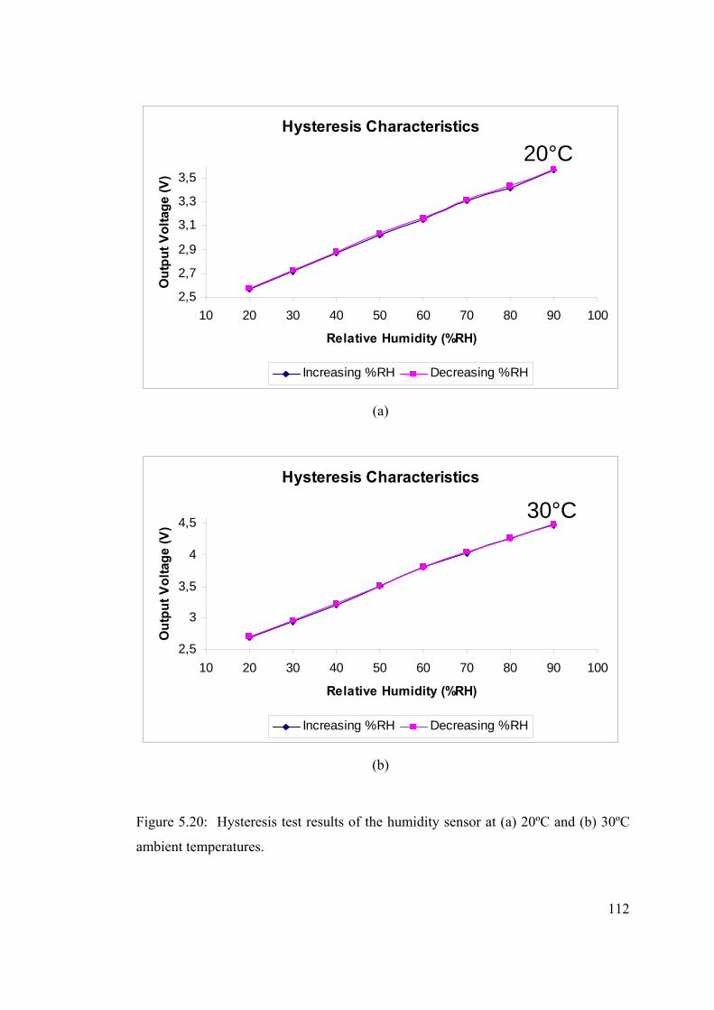
112
Hysteresis Characteristics
2,5
2,7
2,9
3,1
3,3
3,5
10 20 30 40 50 60 70 80 90 100
Relative Humidity (%RH)
Out
put V
olta
ge (V
)
Increasing %RH Decreasing %RH
20°C
(a)
Hysteresis Characteristics
2,5
3
3,5
4
4,5
10 20 30 40 50 60 70 80 90 100
Relative Humidity (%RH)
Out
put V
olta
ge (V
)
Increasing %RH Decreasing %RH
30°C
(b)
Figure 5.20: Hysteresis test results of the humidity sensor at (a) 20ºC and (b) 30ºC
ambient temperatures.
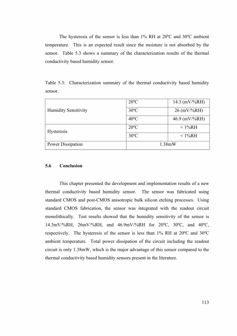
113
The hysteresis of the sensor is less than 1% RH at 20ºC and 30ºC ambient
temperature. This is an expected result since the moisture is not absorbed by the
sensor. Table 5.3 shows a summary of the characterization results of the thermal
conductivity based humidity sensor.
Table 5.3: Characterization summary of the thermal conductivity based humidity
sensor.
20ºC 14.3 (mV/%RH)
30ºC 26 (mV/%RH) Humidity Sensitivity
40ºC 46.9 (mV/%RH)
20ºC < 1%RH Hysteresis
30ºC < 1%RH
Power Dissipation 1.38mW
5.6 Conclusion
This chapter presented the development and implementation results of a new
thermal conductivity based humidity sensor. The sensor was fabricated using
standard CMOS and post-CMOS anisotropic bulk silicon etching processes. Using
standard CMOS fabrication, the sensor was integrated with the readout circuit
monolithically. Test results showed that the humidity sensitivity of the sensor is
14.3mV/%RH, 26mV/%RH, and 46.9mV/%RH for 20ºC, 30ºC, and 40ºC,
respectively. The hysteresis of the sensor is less than 1% RH at 20ºC and 30ºC
ambient temperature. Total power dissipation of the circuit including the readout
circuit is only 1.38mW, which is the major advantage of this sensor compared to the
thermal conductivity based humidity sensors present in the literature.
114
6. CHAPTER 6
CONCLUSIONS AND FUTURE WORK
This thesis presents the design and implementation of humidity sensors using
MEMS and standard CMOS technologies. Two different humidity sensors were
implemented using capacitive and thermal conductivity based humidity measurement
techniques. The capacitive humidity sensor was hybrid connected to a CMOS
switched capacitor readout circuit, which is also developed in this study; while the
thermal conductivity based humidity sensor was monolithically integrated with the
readout circuit using standard CMOS fabrication and post-CMOS processing.
Achievements of this research can be summarized as follows:
1. A capacitive humidity sensor with an integrated heater was designed and
fabricated by three mask surface micromachining process using the clean
room facilities of METU. The sensor was characterized by monitoring the
humidity response, hysteresis characteristics, and measuring the response
time in an environmental chamber. The operation of the integrated heater
was verified by measuring the resistance versus temperature and resistance
versus heating power characteristics.
2. A switched capacitor readout circuit was designed and fabricated in the AMS
0.8µm CMOS process. The readout circuit was connected to the sensor by
wire bonding on an alumina substrate, which is attached to a commercial
package. The hybrid module was characterized inside the environmental
CHAPTER 6
115
chamber. Sensitivity of the sensor was found as 19.4mV/%RH, with a
nonlinearity of 0.17%. Hysteresis of the sensor was found as 2.54% RH.
3. A thermal conductivity based humidity sensor, which is monolithically
integrated with the readout circuit was designed and implemented in the AMS
0.6µm CMOS process. The fabrication was completed by post-CMOS
anisotropic bulk silicon etching process and electrochemical etch-stop
techniques.
4. The thermal conductivity based humidity sensor was characterized by
measuring the humidity response and the hysteresis characteristics. A proper
test setup was prepared on a printed circuit board for the characterization
measurements. The sensor provides a sensitivity of 14.3mV/%RH,
26mV/%RH, and 46.9mV/%RH for 20ºC, 30ºC, and 40ºC ambient
temperatures respectively. The sensing diodes are heated up to 250ºC, so the
sensor does not allow water condensation. Total power dissipation of the
sensor is only 1.38mW.
Although the major goals of this research were achieved, following tasks can
be suggested as future work:
1. Different polyimide types, which allow the formation of thinner dielectric
layers, can be used as the humidity sensitive layer in order to obtain higher
sensitive capacitive humidity sensors. Another alternative is to use glass
substrate instead of a silicon substrate.
2. The capacitive humidity sensor can be implemented on a diaphragm to
provide thermal isolation from the substrate in order to operate the integrated
heater with less power.
116
3. The integrated heater of the capacitive humidity sensor can be fabricated
from a metal, which has less thermal conductivity than aluminum in order to
increase the power efficiency of the heater.
4. Die level packaging of the thermal conductivity based humidity sensor needs
to be completed in order to complete the fabrication of the sensor as a
prototype for mass production.
This study is the first national study to implement humidity sensors using
MEMS and silicon micromachining technologies, and it is hoped that the results of
this study can be used to implement humidity sensors to be used in industry.
117
REFERENCES
[1] H. L. Penman, Humidity, The Institute of Physics, London, 1955. [2] F. W. Gole, Introduction to Meteorology, John Wiley & Sons Inc., New York,
1970. [3] G. J. Visscher, “Standard Psychrometers: a matter of preferences,” Meas. Sci.
Technology, Vol. 6, pp. 1451-1461, 1995.
[4] Z. M. Rittersma, “Recent Achievements in Miniaturized Humidity Sensors-a Review of Transduction Techniques,” Sensors and Actuators A, Vol. 96, pp. 196-210, 2002.
[5] L. J. Golonka, B. W. Licznerski, K. Nitsch, H. Terycz, “Thick Film Humidity
Sensors,” Measurement Science and Technology, Vol. 8, pp. 92-98, 1997. [6] E. Traversa, “Ceramic Sensors for Humidity Detection: the State of the Art and
Future Developments,” Sensors and Actuators B, Vol. 23, pp. 1335-1356, 1995. [7] N. Serin, T. Serin, B. Unal, “The Effect of Humidity on Electronic Conductivity
of an Au/CuO/Cu2O/Cu Sandwich Structure,” Semiconductor Science and Technology, Vol. 15, pp.112-116, 2000.
[8] S. Chakraborty, “The Humidity Dependent Conductance of Al2(SO4)3.16H2O,”
Smart Materials and Structures, Vol. 4, pp. 368-369, 1995. [9] W. Qu, J. U. Meyer, “Thick Film Humidity Sensors Based on Porous MnWO4
Material,” Measurement Science and Technology, Vol. 8, pp. 593-600, 1997. [10] W. Qu, R. Green, M. Austin, “Development of Multi-Functional Sensors in
Thick-Film and Thin-Film Technology,” Measurement Science and Technology, Vol. 11, pp. 1111-1118, 2000.
[11] H. Wang, C. D. Feng, S. L. Sun, C. U. Segre, J. R. Stetter, “Comparison of
Conductometric Humidity Sensing Polymers,” Sensors and Actuators B, Vol. 40, pp. 211-216 ,1997.
[12] C. D. Feng, S. L. Sun, H. Wang, C. U. Segre, J. R. Stetter, “Humidity Sensitive
Properties of Nafion and Sol-gel Derived SiO2/Nafion Composite Thin Films,” Sensors and Actuators B, Vol. 40, pp. 217-222, 1997.
[13] Y. Sakai, M. Matsuguchi, H. Makihata, “A New Type LiCl Dew Point
Hygrometer Probe Fabricated with a Composite of Porous Polymer and the
118
Salt,” The 10th International Conference on Solid-State Sensors and Actuators (TRANSDUCERS’99), pp. 1664-1667, Sendai, Japan, June 1999.
[14] K. Sager, A. Schroth, A. Nakladal and G. Gerlach, “Humidity-Dependent
Mechanical Properties of Polyimide Films and Their Use for IC-Compatible Humidity Sensors,” Sensors and Actuators A Vol. 53, pp. 330-334, 1996.
[15] R. Buchhold, A. Nakladal, G. Gerlach, P. Neumann, “Design Studies on
Piezoresisitive Humidity Sensors,” Sensors and Actuators B, Vol. 53, pp. 1-7, 1998.
[16] N. T. T. Ha, D. K. An, P. V. Phong, P. T. N. Hoa, L. H. Mai, “Study and
Performance of Humidity Sensor Based on the Mechanical-Optoelectronic Principle for the Measurement and Control of Humidity in Storehouses,” Sensors and Actuators B, Vol. 66, pp. 200-202, 2000.
[17] E. Radeva, V. Georgiev, L. Spassov, N. Koprinarov, St. Kanev, “Humidity
Absorptive Properties of Thin Fullerene Layers Studied by Means of Quartz Microbalance,” Sensors and Actuators B, Vol. 42, pp. 11-13, 1997.
[18] F. Pascal-Delannoy, B. Sorli, A. Boyer, “Quartz Crystal Microbalance (QCM)
Used as Humidity Sensor,” Sensors and Actuators A, Vol. 84, pp. 285-291, 2000.
[19] J. Reibel, U. Stahl, T. Wessa, M. Rap, “Gas Analysis with SAW Sensor
Systems,” Sensors and Actuators B, Vol. 65, pp. 173-175, 2000. [20] E. T. Zellers, M. Morishita, Q. C. Cai, “Evaluating Porous Layer Open-Tubular
Capillaries as Vapor Preconcentrators in a Microanalytical System,” Sensors and Actuators B, Vol. 67, pp. 244-253, 2000.
[21] C. Bariain, R. Matias, F. J. Arregui, M. Amo, “Optical Fiber Humidity Sensor
Based on a Tapered Fiber Coated with Agarose Gel,” Sensors and Actuators B, Vol. 69, pp. 127-131, 2000.
[22] F. Arregui, Y. Liu, R. Matias, R. Claus, “Optical Fiber Humidity Sensor Using a
Nano Fabry-Perrot Cavity Formed by the Ionic Self-Assemblt Method,” Sensors and Actuators B, Vol. 59, pp. 54-59, 1999.
[23] B.C. Gupta, Ratnanjali, “A Novel Probe for a Fiber Optic Humidity Sensor,”
Sensors and Actuatros B, Vol. 80, pp. 132-135, 2001. [24] M. Kimura, “A New Method to Measure the Absolute Humidity Independently
of the Ambient Temperature,” The 8th International Conference on Solid-State Sensors and Actuators (TRANSDUCERS’95), pp. 843-846, Stockholm, Sweden, 1995.
119
[25] D. Lee, H. Hong, C. Park, G. Kim, Y. Jeon, J. Bu, “A Micromachined Robust
Humidity Sensor for Harsh Environment Applications,” The 14th IEEE International Conference on Micro Electro Mechanical Systems (MEMS 2001), pp. 558-561, January 2001.
[26] W. Qu, W. Wlodarski, “A Thin-film Sensing Element for Ozone, Humidity and
Temperature,” Sensors and Actuators B, Vol. 64, pp. 42-48, 2000. [27] W. Qu, J. Meyer, “A Novel Thick Film Humidity Sensor,” Sensors and
Actuators B, Vol. 40, pp. 175-182, 1997. [28] C.M.A. Ashruf, P.J. French, P.M.M.C. Bressers, J.J. Kelly, “Galvanic Porous
Silicon Formation without External Contacts,” Sensors and Actuators A, Vol. 74, pp. 118-122, 1999.
[29] Z.M. Rittersma, A. Splinter, A. Bödecker, W. Benecke, “A Novel Surface
Micromachined Capacitive Porous Silicon Humidity Sensor,” Sensors and Actuators B, Vol. 68, pp. 210-217, 2000.
[30] A. Foucaran, B. Sorli, M. Garcia, F. Pascal-Delannoy, A. Giani, A. Boyer,
“Porous Silicon Layer Coupled with Thermoelectric Cooler: a Humidity Sensor,” Sensors and Actuators A, Vol. 79, pp. 189-193, 2000.
[31] M. Matsuguch, T. Kuroiwa, T. Miyagishi, S. Suzuki, T. Ogura, Y. Sakai,
“Stability and Reliability of Polyimide Humidity Sensors Using Crosslinked Polyimide Films,” Sensors and Actuators B, Vol. 52, pp. 53-57, 1998.
[32] A. R. K. Ralston, C. F. Klein, P. E. Thoma and D. D. Denton, “A model for the
relative environmental stability of a series of polyimide capacitance humidity sensors,” Sensors and Actuators B, Vol. 34, pp. 343-348, 1996.
[33] R. Jachowicz, J. Weremczuk, “Sub-cooled Water Detection in Silicon Dew
Point Hygrometer,” Sensors and Actuators A, Vol. 85, pp. 75-83, 2000. [34] U. Kang, K. D. Wise, “A High Speed Capacitive Humidity Sensor with On-
Chip Thermal Reset,” IEEE Transactions on Electron Devices, Vol. 47, pp. 702-710, 2000.
[35] C. Laville, C. Pellet, “Interdigitated Humidity Sensors for a Portable Clinical
Microsystem,” IEEE Transactions on Biomedical Engineering, Vol. 49, pp.1162-1167, 2002.
[36] Y. Y. Qui, C. Azeredo-Leme, L. R. Alcacer, J. E. Franca, “A CMOS Humidity
Sensor with On-Chip Calibration,” Sensors and Actuators A, Vol. 92, pp. 80-87, 2001.
120
[37] M. Dokmeci, K. Najafi, “A high-sensitivity polyimide capacitive relative humidity sensor for monitoring anodically bonded hermetic micropackages,” IEEE Journal of Microelectromechanical Systems, Vol. 10, pp. 197-204.
[38] A. R. K. Ralston, M. C. Buncick, and D. D. Denton, “Effects of Aging on
Polyimide: A Model for Dielectric Behavior”, The 6th International Conference on Solid-State Sensors and Actuators (TRANSDUCERS’91), pp. 759-763.
[39] S. D. Senturia, Microsystem Design, Kluwer Academic Publishers,
Massachusetts, 2001. [40] B. Wang, T. Kajita, T. Sun, G. Temes, “New High Precision Circuits for on-
chip Capacitor Ratio Testing and Sensor Readout,” The 8th International Conference on Solid-State Sensors and Actuators (TRANSDUCERS’95), pp. 138-141, Stockholm, Sweden, 1995.
[41] X. Li, G. Meijer, “An Accurate Interface for Capacitive Sensors,” IEEE
Transactions on Instrumentation and Measurement, Vol. 51, pp. 935-939, 2002. [42] X. Shi, H. Matsumoto, K. Murao, “A High Accuracy Digital Readout Technique
for Humidity Sensor,” IEEE Transactions on Instrumentation and Measurement, Vol. 50, pp. 1277-1280, 2001.
[43] M. Pedersen, W. Olthius, P. Bergveld, “An Integrated Silicon Capacitive
Microphone with Frequency Modulated Digital Output,” Sensors and Actuators A, Vol. 69, pp. 267-275, 1998.
[44] T. Bolthauser, C. Leme, H. Baltes, “High Sensitivity CMOS Humidity Sensors
with on-chip Absolute Capacitance Measurement System,” Sensors and Actuators B, Vol. 15, pp. 75-80, 1993.
[45] R. Gregorian, Introduction to CMOS Op-Amps and Comparators, John Wiley &
Sons Inc., 1999. [46] J. E. France, Y. Tsividis, Design of Analog-Digital VLSI Circuits for
Telecommunications and Signal Processing, Prentice Hall 1994. [47] C. Laville, C. Pellet, “Comparison of Three Humidity Sensors for a Pulmonary
Function Diagnosis Microsystem,” IEEE Sensors Journal, Vol. 2, pp. 96-101, 2002.
[48] T. Ishikava, M. Ueno, Y. Nakaki, K. Endo, Y. Ohta, J. Nakanishi, Y.
Kosasayama, H. Yagi, T. Sone, M. Kimata, “Performance of 320x240 Uncooled IRFPA with SOI Diode Detectors,” Proceedings of SPIE, Vol. 4130, pp. 1-8, 2000.
121
[49] S. Eminoglu, D. Tezcan, M. Tanrikulu, T. Akin, “A Low-Cost, Small Pixel Uncooled Infrared Detector for Large Focal Plane Arrays Using a Standard CMOS Process,” Proceedings of SPIE, Vol. 4721, pp. 111-121, 2002.
[50] S. Eminoglu, D. Tezcan, M. Tanrikulu, T. Akin, “Low-Cost Uncooled Infrared
Detectors in CMOS Process,” The 16th European Conference on Solid State Transducers (Eurosensors XVI), pp. 263-264, Prague, Czech Republic, September 2002.
[51] D. Hodges, H. Jackson, Analysis and Design of Digital Integrated Circuits,
McGraw-Hill, 1988. [52] P. W. Kruse, D. D. Skatrud, Uncooled Infrafer Imaging Arrays and Systems,
Semiconductors and Semimetals 47, Academic Press 1997. [53] S. Eminoglu, M. Y. Tanrikulu, T.Akin, “A Low-Cost 64x64 Uncooled Infrared
Detector in Standard CMOS,” The 12th International Conference on Solid-State Sensors, Actuators, and Microsystems (TRANSDUCERS’03), pp. 316-319, Boston, USA, June 2003.
[54] N. Maluf, An Introduction to Microelectromechanical Systems Engineering,
Artech House, 2000. [55] G. Yan, P. Chan, M. Hsing, R. Sharma, J. Sin, Y. Wang, “An Improved TMAH
Si-etching Solution Without Attacking Exposed Aluminum,” Sensors and Actuators A, Vol. 89, pp. 135-141, 2001.
[56] S. M. Sze, Semiconductor Sensors, John Wiley and Sons, 1994. [57] M. Parameswaran, H. Baltes, L. Ristic, D. Dhaded, and A. Robinson, “A New
Approach for the Fabrication of Micromechanical Structures,” Sensors and Actuators A, Vol. 19, pp. 289-307, 1989.
[58] HIH-3610 Series Humidity Sensor Product Sheet, Honeywell. [59] http://www.wpi.edu.
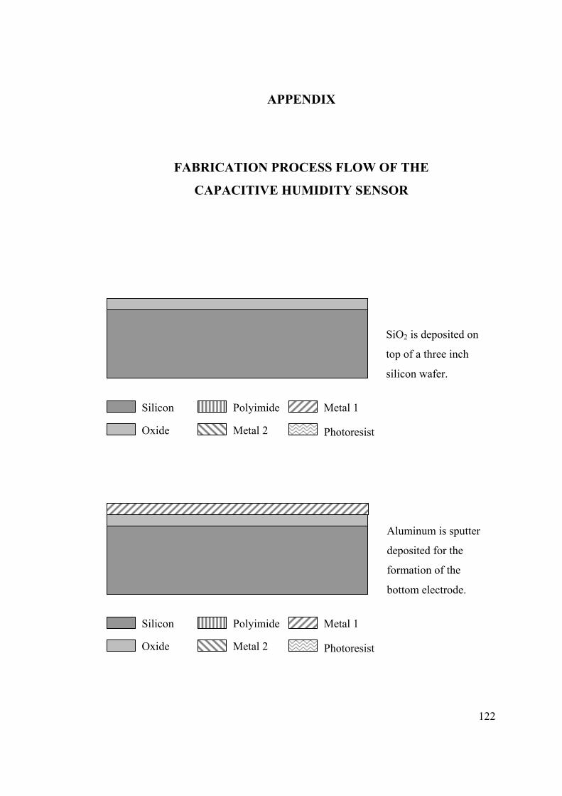
122
APPENDIX
FABRICATION PROCESS FLOW OF THE
CAPACITIVE HUMIDITY SENSOR
Silicon
Oxide
Metal 1Polyimide
Metal 2
Silicon
Oxide
Metal 1Polyimide
Metal 2
SiO2 is deposited on
top of a three inch
silicon wafer.
Aluminum is sputter
deposited for the
formation of the
bottom electrode.
Photoresist
Photoresist
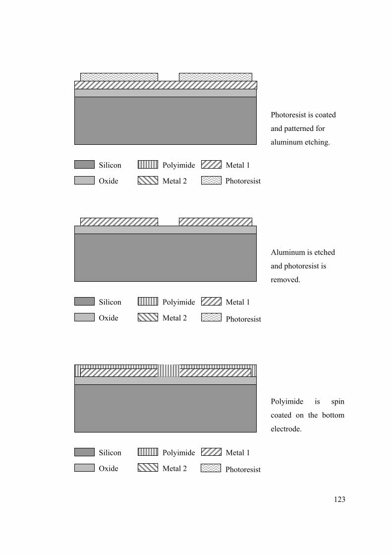
123
Silicon
Oxide
Metal 1Polyimide
Metal 2
Silicon
Oxide
Metal 1Polyimide
Metal 2
Silicon
Oxide
Metal 1Polyimide
Metal 2 Photoresist
Photoresist is coated
and patterned for
aluminum etching.
Aluminum is etched
and photoresist is
removed.
Polyimide is spin
coated on the bottom
electrode.
Photoresist
Photoresist
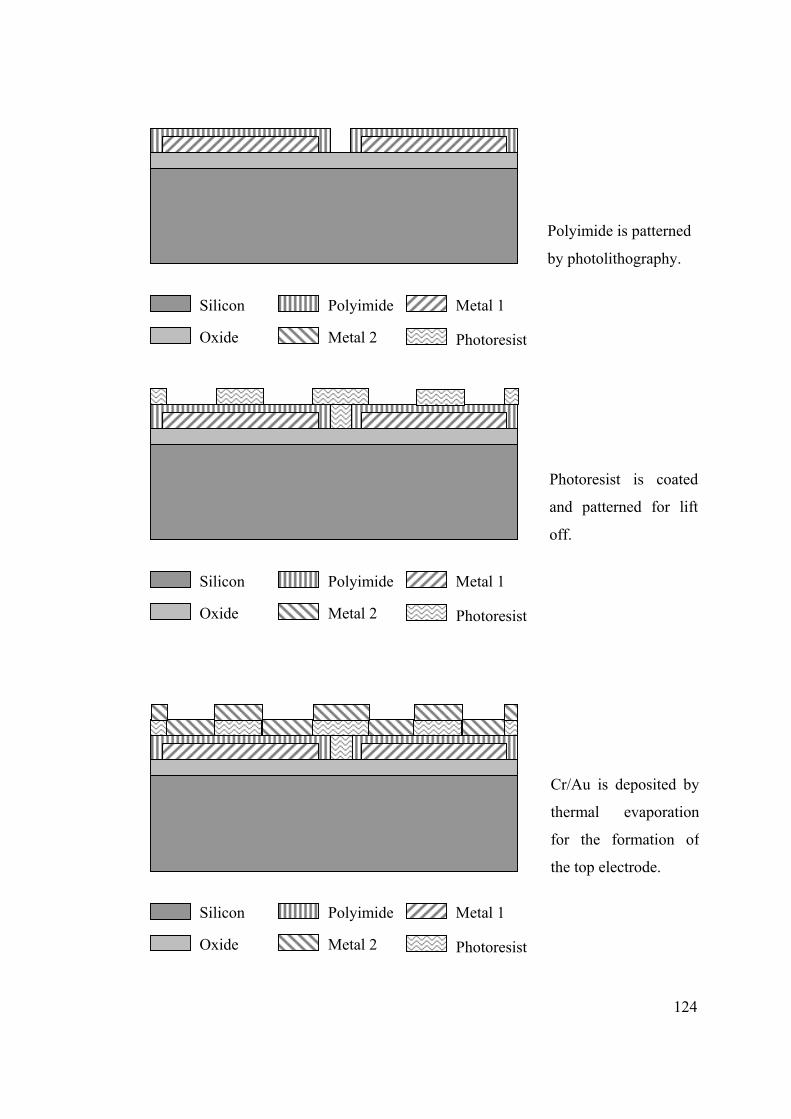
124
Silicon
Oxide
Metal 1Polyimide
Metal 2
Silicon
Oxide
Metal 1Polyimide
Metal 2
Silicon
Oxide
Metal 1Polyimide
Metal 2
Polyimide is patterned
by photolithography.
Photoresist is coated
and patterned for lift
off.
Cr/Au is deposited by
thermal evaporation
for the formation of
the top electrode.
Photoresist
Photoresist
Photoresist
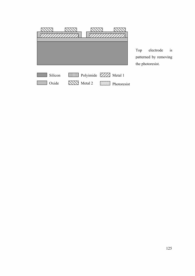
125
Silicon
Oxide
Metal 1Polyimide
Metal 2
Top electrode is
patterned by removing
the photoresist.
Photoresist
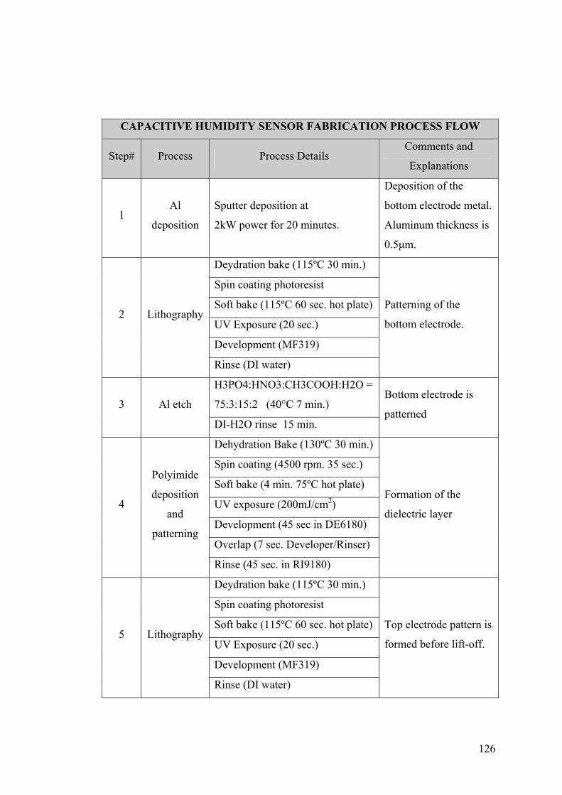
126
CAPACITIVE HUMIDITY SENSOR FABRICATION PROCESS FLOW
Step# Process Process Details Comments and
Explanations
1 Al
deposition
Sputter deposition at
2kW power for 20 minutes.
Deposition of the
bottom electrode metal.
Aluminum thickness is
0.5µm.
Deydration bake (115ºC 30 min.)
Spin coating photoresist
Soft bake (115ºC 60 sec. hot plate)
UV Exposure (20 sec.)
Development (MF319)
2 Lithography
Rinse (DI water)
Patterning of the
bottom electrode.
H3PO4:HNO3:CH3COOH:H2O =
75:3:15:2 (40°C 7 min.) 3 Al etch
DI-H2O rinse 15 min.
Bottom electrode is
patterned
Dehydration Bake (130ºC 30 min.)
Spin coating (4500 rpm. 35 sec.)
Soft bake (4 min. 75ºC hot plate)
UV exposure (200mJ/cm2)
Development (45 sec in DE6180)
Overlap (7 sec. Developer/Rinser)
4
Polyimide
deposition
and
patterning
Rinse (45 sec. in RI9180)
Formation of the
dielectric layer
Deydration bake (115ºC 30 min.)
Spin coating photoresist
Soft bake (115ºC 60 sec. hot plate)
UV Exposure (20 sec.)
Development (MF319)
5 Lithography
Rinse (DI water)
Top electrode pattern is
formed before lift-off.
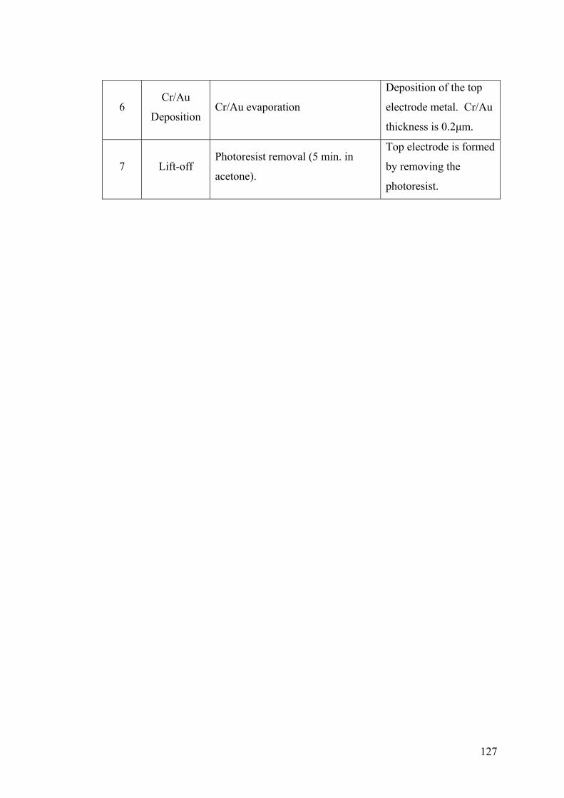
127
6 Cr/Au
Deposition Cr/Au evaporation
Deposition of the top
electrode metal. Cr/Au
thickness is 0.2µm.
7 Lift-off Photoresist removal (5 min. in
acetone).
Top electrode is formed
by removing the
photoresist.