i2c_over
TRANSCRIPT

8/12/2019 i2c_over
http://slidepdf.com/reader/full/i2cover 1/7
I2C Overview February 19, 1998 Page 1 of 7
Overview of the Inter-Integrated Circuit (I2C) Bus
ECPE 4536
Microprocessor System Design II
Virginia Tech
The Inter-Integrated Circuit (I2C) Bus, developed and patented by Philips, is a simple, low-cost serialinterface for connecting one or more microcontrollers and peripherals in an embedded system.
Components available with an I2C Bus interface include microcontrollers, LCD drivers, I/O expanders,
memory, analog-to-digital and digital-to-analog converters, clock/calendars, and application-specific ICssuch as voice synthesizers, transcoders for infrared remote controls, picture-in-picture controllers, and
frequency synthesizers for mobile telephones. The I2C Bus defines the signals, data formats, and protocols
necessary for devices to communicate. This document provides information about the I2C Bus that will beneeded for a project. It is not intended as a comprehensive description of the bus. Specifically, only basic
addressing modes and the low-speed mode of operation are discussed in detail.
Rp
+VDD
Rp
+VDD
SCL
SDA
µC
A
µC
B
Device
a
Device
b
Device
c
Figure 1. Example I2C Bus system.
1. Basic Operation
A typical I2C Bus configuration is shown in Figure 1. The I2C Bus defines two signals (wires), SDA for
serial data and SCL for serial clock, to carry information between devices. Each device is identified by a
unique address. Each device can either transmit data or receive data. A device operates as either a master
or as a slave. A master initiates data transfer, either to or from one or more slaves, and generates clock signals. The device addressed by the master is considered, at that time, to be a slave. For example, if
microcontroller A (µC A) in the figure addresses and sends data to Device a, perhaps an LCD driver, then
µC A is the master and Device a is the slave. In this case, µC A generates the clock signal on SCL, sends
the address, and sends the data. Suppose µC A wanted to receive data from Device b, say a memory
device. Then, as master, µC A generates the clock signal on SCL and sends the address, but Device bsends data back to the microcontroller.
The I2C Bus supports multiple masters, i.e. more than one device is capable of controlling the bus. In the
example shown in the figure, both µC A and µC B can act as masters. The I2C Bus includes an arbitration
scheme so that correct operation will occur if more than one master wants to use the bus at the same time.
Note that the master and slave relationships are dynamic. For example, µC B can address µC A and send it
data. In this case, µC B acts as a transmitting master and µC A acts as a receiving slave. Later, µC A
might address and send data to µC B, in which case the master and slave roles are reversed.
Clock generation is the responsibility of the master. However, slave devices can “stretch” clock cycles by
holding the clock low. This allows devices of different speeds to be connected to the bus.

8/12/2019 i2c_over
http://slidepdf.com/reader/full/i2cover 2/7
I2C Overview February 19, 1998 Page 2 of 7
2. SCL and SDA Characteristics
SCL and SDA are bidirectional lines. Any device acting as a master must be able to both drive and sense
SCL and SDA. Any device acting as a slave must be able to sense SCL and drive and sense SDA. A slavemay also drive SCL to stretch a clock cycle.
SCL and SDA are connected to a positive supply voltage (VDD = +5 V for TTL logic) through pull-up
resistors (RP = 2.7 KΩ for our purposes) and are driven by open-collector devices (7407 TTL non-invertingopen-collector drivers for our project). If any device outputs a low (0), then the signal is low. The signal is
high (1) if and only if all devices are driving the signal high. Thus, SCL and SDA each implement a
“wired-AND” function.
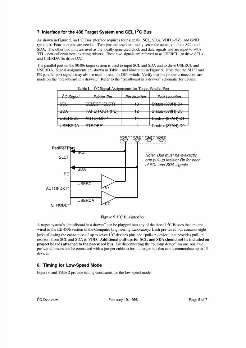
3. Data Transfer
3.1. Format
Figure 2 shows a data format for an I2C Bus transaction. The unit of information including start condition,
address, data, acknowledgment, and stop condition is sometimes referred to as a frame and constitutes an
atomic transfer as defined for the I2C Bus. A higher level protocol may use the I2C Bus to transfer
multiple frames, but the I2C Bus itself defines no relationship between different frames.
Sstartbyte
addressA SrR/ W
data A data A... PS = start conditionSr = restartA = acknowledgeP = stop condition
8 1 7 1 8 1 8 1
A
1
Figure 2. Data transfer format for low-speed mode.
As shown in the figure, a master generates a start condition (S) to change the bus from an idle state to a
busy state and begin the transaction. A master cannot begin a frame unless the bus is idle. If two or more
masters attempt to use the bus at approximately the same time, an arbitration procedure determines which
master may use the bus. Section 5 describes arbitration.
For a low-speed mode transfer (as used in the project), the start condition is followed by a special start byte(00000001B) and dummy acknowledgment. Another start condition, called a repeated start or restart (Sr),
is generated immediately after the dummy acknowledgment (A). The start byte permits a slow device, such
as a microprocessor implementing the I2C Bus interface in software, to poll for bus activity less often. The
slow device can detect bus activity at any point during the start byte and then detect the restart.
Following the restart, the master sends a byte that consists of a seven-bit address and a read/write (R / W)
command bit. Each device can compare the transmitted address to its own address. If they are equal, thenthe device is being addressed as a slave. If they are not equal, then the device ignores the rest of the
transaction. The R / W bit indicates if the master wishes to receive data (R / W=1) or transmit data
(R / W=0).
The selected slave device follows the address and read/write byte with an acknowledgment (A). A=0 is a
positive acknowledgment that indicates to the master that the slave is responding. If A=1, then the mastermust assume that the addressed slave is not responding. The I2C Bus does not define error recovery
procedures.
Zero or more data bytes follow. The I2C Bus does not define a maximum number of bytes that can be
transferred in one frame. The master drives the data on SDA for a write operation and the slave drives dataon SDA for a read operation. Each data byte is followed by an acknowledgment. The acknowledgment is
always generated by the device receiving data, i.e. the slave for a write and the master for a read.

8/12/2019 i2c_over
http://slidepdf.com/reader/full/i2cover 3/7
I2C Overview February 19, 1998 Page 3 of 7
When the master is finished sending or receiving data, it generates a stop condition (P) and the bus returns
to an idle state. The master will also generate a stop condition in the event of an error. For example, if the
slave does not respond to the address sent by the master, then the master generates a stop condition.
3.2. Start Condition
Normally the SDA line must be held stable during a high clock (SCL) pulse. The start condition (S) and
stop condition (P) are two exceptions. A high-to-low transition on SDA while SCL is high indicates a start.The start condition is always generated by a master. Figure 3 shows a low-speed mode data transfer. The
start condition (S) occurs at the beginning of the transfer. A repeated start condition (Sr) occurs after the
start byte.
S
1 2-7 8 9SCL
SDA
Sr
1-7 8 9
R/W
start byte A address A
1-7 8 9
A Pdata byte(s)
Figure 3. Low-speed mode data transfer.
3.3. Bit Transfer
Figure 4 shows a bit transfer on the I2C Bus. Data on SDA remains valid while the clock, SCL, is high.
Certain timing constraints must be met, as described in Section 8.
If the master is transferring data on a write operation, it will pull the clock low, drive the next bit onto
SDA, and then release the clock (set it high). The master will continue to drive SDA until it again pulls
SCL low.
SCL
SDA
datacan
change
datacannotchange
Figure 4. Bit transfer.
If the slave is transferring data on a read operation, it will wait until the master pulls the clock low and then
drive the next bit onto SDA. It will hold this value on SDA until the master again pulls the clock low.
3.4. Byte Transfer
Every byte transferred must be eight bits in length. Each byte must be followed by an acknowledgment bit.
The most significant bit (msb) is transmitted first and the least significant bit (lsb) is transmitted last.
3.5. Acknowledge
An acknowledgment bit (A) must be sent after each byte is received, as shown in Figures 2 and 3. The
master generates the clock pulse on SCL for the acknowledge bit, while the data receiver generates the

8/12/2019 i2c_over
http://slidepdf.com/reader/full/i2cover 4/7
I2C Overview February 19, 1998 Page 4 of 7
acknowledge bit on SDA. The transmitter must release SDA (high output) during the acknowledge clock
pulse.
When a slave does not acknowledge the slave address transmitted by the master, the data line is left high.
The master should then generate a stop condition to terminate the transfer. When a slave acknowledges its
address, but cannot receive any more data bytes, it does not generate an acknowledge on the followingbyte. The master then generates a stop condition.
When a master is receiving data from a slave, it does not acknowledge the last byte that it wishes to
receive. The slave then releases the data line, allowing the master to generate a stop condition.
3.6. Stop Condition
A low-to-high transition on SDA while SCL is high indicates a stop condition (P), as shown in Figure 3-3.
The stop condition is always generated by the master.
4. Clock Generation
The wired-AND function of the SCL lines supports clock synchronization. The master normally pulls SCL
low at the end of a high clock period. At the end of the low period, it releases SCL by setting its clock
output to high. However, SCL will not go high until all devices have released the clock. The master waits
until SCL actually goes high before it begins timing the high clock pulse. Thus, a slave may pull SCL lowif it needs additional time before the next high clock pulse.
5. Arbitration
A master cannot attempt to transfer data unless the bus is idle, i.e. SDA and SCL are both high following a
stop condition. However, it may be that two or more masters sense an idle bus and attempt to use the bus
(drive SDA) at nearly the same time. An arbitration procedure ensures a valid transfer by one of themasters in this situation.
The arbitration scheme used on the I2C Bus grants the bus to the first master that generates a low (0) on
SDA while the other master generates a high (1). If during a high clock pulse a master that outputs a high
on SDA detects that SDA is low, then it knows that another master must be transmitting. The master
generating the high loses arbitration and releases SDA (sets its data output high). The “losing” master maycontinue to generate clock pulses until the end of the byte in which it loses arbitration. The “winning”
master continues with its data transfer.
Arbitration can continue through many bits. If the masters are transmitting to different slaves, then
arbitration will terminate with the first difference in address bits. If the masters are transmitting to the sameslave, then arbitration will continue into the data. Because the winning master's data is transmitted
properly, no data is lost. The losing master must recognize that it has lost arbitration and attempt its
transfer later, if appropriate.
A tricky situation occurs when a master loses arbitration during the address byte. It is possible that the
winning master is trying to address the losing master as a slave. Therefore, the losing master must
immediately switch to slave receiver mode. This implies that a master must collect the address byte being
transmitted over the I2C Bus and, if it loses arbitration during the address byte, check the address to see if it
matches its own address.
6. Addresses
Device addresses are seven bits long are unique for every device. The seven-bit device address and the
R / W bit together form an eight-bit address byte. Certain addresses are reserved. For example, the startbyte (00000001B) is a reserved address byte so that no slave device will respond to the start byte as an
address.
8/12/2019 i2c_over
http://slidepdf.com/reader/full/i2cover 5/7

8/12/2019 i2c_over
http://slidepdf.com/reader/full/i2cover 6/7
I2C Overview February 19, 1998 Page 6 of 7
tBUF tR
tLOWtHD;STA
tF
tHIGH
SDA
SCL
tHD;DAT
tSU;DAT
P S
tSU;STA
tHD;STA
Sr
tSU;STO
Figure 6. Timing for low-speed mode.
Table 2. I2C Low-Speed Mode Timing Parameter Values
Symbol Parameter Limits Unit
MIN MAX
TBUF Time the bus must be idle before a new transmission can start. 105 µs
tHD;STA Hold time start condition. After this period the first clock pulse isgenerated.
365 µs
tHD;STA Hold time (repeated start condition only). 210 µs
TLOW Low period of clock. 105 155 µs
THIGH High period of clock. 365 415 µs
tSU;STA Setup time for start condit ion (repeated start condition only). 105 155 µs
tHD;DAT Hold time for data. 0 µs
tSU;DAT Setup time for data. 250 ns
TR Rise time for both SDA and SCL lines. 1 µs
TF Fall time for both SDA and SCL lines. 300 ns
tSU;STO Setup time for stop condition. 105 155 µs
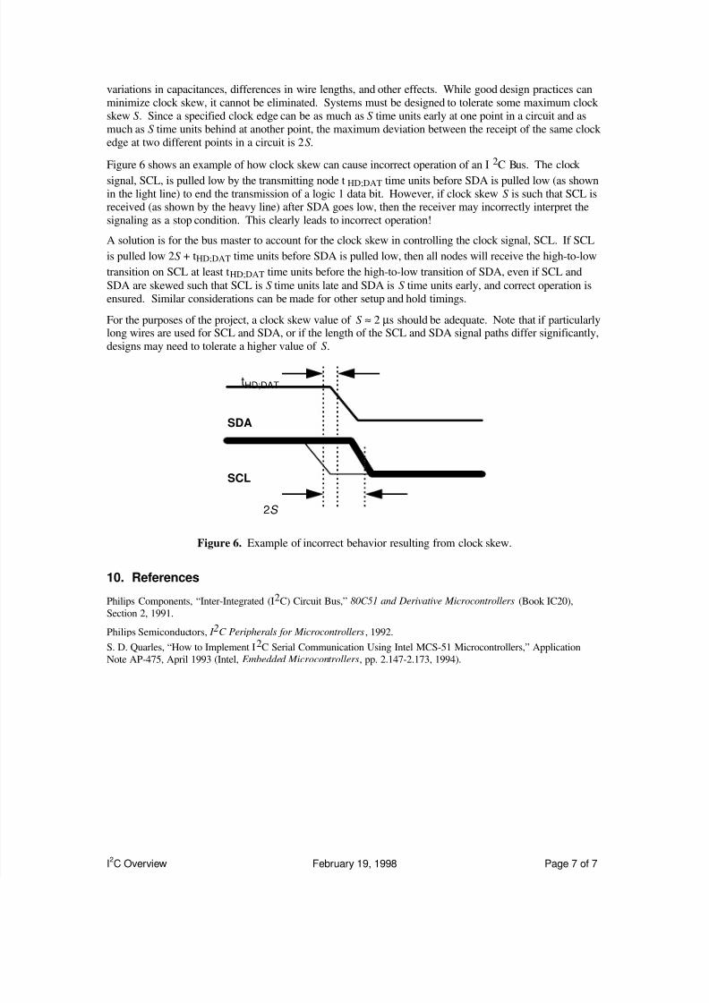
9. Clock Skew
Clock skew is defined to be the uncontrolled and random deviation from the nominal timing of the leading
edge of a given clock signal at a given clock input.1 Clock skew results from physical factors such as
1 S. H. Unger and C.-J. Ten, “Optimal Clocking Schemes for High Speed Digital Systems,” Proc. Int’l.
Conf. on Computer Design, 1983, pp. 366-369.
8/12/2019 i2c_over
http://slidepdf.com/reader/full/i2cover 7/7