ia # oif-m sa-100g - optical internetworking forum · 08.05.2015 · 100 orig ia p imp g lon mod...
TRANSCRIPT
100
OrigIA p
Imp
0G LonMod
(
IA
ginal Veassed p
Implementby th
plemen
Genng-Haudule – (Gen.2
A # OIF-M
ersion 2principa
tation Agrehe Optical I
www.
ntationFor
neratioul DWD Electro MSA-1
MSA-100G
.0 Apprl ballot
eement creanternetwor.oiforum.co
O
n Agree on 2.0 DM Tromecha100GL
GLH-EM
roved 25t 31st M
ated and aprking Forumom
OIF-MSA-100
ement
ansmisanical
LH)
M-02.1
5th ApriMarch 20
pproved m
0GLH-EM-02
ssion
l 2013 15
2.1
Work TITLE
SOUR
ABSTLong-DWDand psupply
king Group:
E: ImplTran
RCE: TE At NE 25 Sa
PhEm
W
KaTr PhEm
TRACT: This -Haul DWDMM transmissio
pin assignmeny, power diss
lementation nsmission M
ECHNICAL Eul SrivastavaEL America, I50 Pehie Ave.addle Brook, Nhone: +1-201-mail: Srivasta
ORKING GR
arl Gass iQuint Semico
hone: +1-505-mail: iamthedo
ImplementatiM Transmissio
on. Key aspent, module hasipation, and m
Physical an
Agreement fodule – Elec
DITOR , Ph. D. nc. ., Suite 706NJ 07663-556-1770va@nel-ame
ROUP VICE C
onductor
-844-8849 onutking@ma
ion Agreemenon Module, fects include: ardware signamanagement
nd Link Laye
for Generatioctromechanic
W D I 1 E P
rica.com E
CHAIR
ac.com
nt specifies kfor applicatiomodule mech
aling pins, higinterface.
O
er (PLL) Work
on 2.0 100G cal (MSA-100
WORKING GDavid R. StauIBM Corporat1000 River REssex Jct., VTPhone: +1-80Email: dstauff
ey electromens such as hanical dimenh-speed elec
OIF-MSA-100
king Group
Long-Haul D0GLH)
GROUP CHAIuffer, Ph. D. tion
Road, MC 862T 05452
02-769-6914 [email protected]
echanical aspe100G PM-QPnsions, electr
ctrical charact
0GLH-EM-02
DWDM
IR
2J
om
ects of a 100PSK long-harical connectoteristics, powe
2.1
G ul or er
www.oi
The includrepreof intechninterc
With OIF aWorkIETF,TMO
NoticofferedresourcNothin
The usemay reimplemimplemwarranthird prights m
© 2011
This dootherwpart, wall suchthe copAgreemBy downotice. perpetu
This doWARRTHE INMERCH
iforum.com
OIF is an iding the wosentatives of
nteroperable, nologies. Opticonnected by
the goal of pactively suppking relations, IP-MPLS F
OC, TMF and
ce: This Technicad to the OIF Memces above. The O
ng in this docume
er's attention is cquire the use of i
mentation agreemmentation of the snty whatsoever, warty, the validitymay or may not b
Optical Internet
ocument and tranwise explain it or without restrictionh copies and deripyright notice or ments. wnloading, copyi Unless the termual and will not b
ocument and theRANTIES, EXPRENFORMATION HHANTABILITY,
internationalorld’s leadin
f the data and cost-effectiical internetw
y optical netw
promoting woports and extships or formorum, IPv6 the CFP MSA
FThe Optical
al Document hasmbership solely aOIF reserves the r
ent is in any way
called to the possinventions cover
ment, the OIF maspecification willwhether expressey of any patent ribe available or th
tworking Forum
nslations of it maassist in its implen other than the fivative works, an references to the
ing, or using thisms and conditions
be revoked by th
information conESS OR IMPLIEDHEREIN WILL N TITLE OR FITN
l non profit ng carriers d optical worive and robworks are dat
working elem
orldwide comtends the womal liaisons hForum, ITU-
A Group.
For additiona Internetwork
Suite 117, F510-492-4040
www
been created bys a basis for agreights to at any tim
y binding on the
sibility that implered by the patentakes no representl not infringe anyed or implied, wights related to ahe terms hereof.
ay be copied andementation may following, (1) thend (2) this docume OIF, except as n
s document in ans of this notice arhe OIF or its succ
ntained herein is D, INCLUDING BNOT INFRINGE
NESS FOR A PAR
organizatioand vendorsrlds, OIF’s p
bust optical ta networks cents.
mpatibility ofork of nationhave been es-T SG13, ITU
al informationking Forum, 4Fremont, CA
0 Φ info@oifor
w.oiforum.com
y the Optical Inteeement and is nome to add, amenOIF or any of its
ementation of tht rights held by thtation or warranty third party righith respect to anyny such claim, o
d furnished to oth be prepared, cope above copyrigh
ment itself may nneeded for the pu
ny manner, the usre breached by thcessors or assigns
provided on an BUT NOT LIMIT ANY RIGHTS O
RTICULAR PURP
O
on with overs. Being an
purpose is to internetworcomposed of
f optical intenal and internstablished wU-T SG15, M
n contact: 48377 Fremon
A 94538 rum.com
m
ernetworking Forot a binding propnd, or withdraw s members.
he OIF implemenhird parties. By pty whatsoever, whts, nor does they claim that has r the extent to w
hers, and derivatpied, published aht notice and thisnot be modified inurpose of develo
ser consents to thhe user, the limits.
“AS IS” basis anTED TO ANY WOR ANY IMPLIEPOSE.
OIF-MSA-100
r 90 memben industry g accelerate thrks and thef routers and
ernetworkingnational stanith IEEE 802
MEF, ATIS-O
nt Blvd.,
rum (OIF). This posal on the comp statements conta
ntation agreemenpublication of th
whether expressee OIF make any rbeen or may be a
which a license to
tive works that cand distributed, s paragraph musn any way, such
oping OIF Implem
he terms and conted permissions g
nd THE OIF DISCWARRANTY THAED WARRANTIE
0GLH-EM-02
er companiegroup unitinhe deploymeneir associate data switche
g products, thndards bodie2.1, IEEE 802.OPTXS, ATIS
document is panies listed as ained herein.
nt contained herehis OIF ed or implied, tharepresentation orasserted by any use any such
comment on or in whole or in st be included on
h as by removing mentation
nditions of this granted above ar
CLAIMS ALL AT THE USE OF ES OF
2.1
3
es, ng nt ed es
he es. 3, S-
ein
at r
n
re
OIF-MSA-100GLH-EM-02.1
www.oiforum.com 4
1 Table of Contents
1 Table of Contents ....................................................................................... 4 2 List of Figures ............................................................................................ 5 3 List of Tables .............................................................................................. 5 4 Document Revision History ...................................................................... 6 5 Introduction ............................................................................................... 7 6 Functional Description .............................................................................. 7 7 Module Management Interface Description ........................................... 10 8 Electrical Specifications ........................................................................... 10
8.1 Operating Case Temperature ............................................................ 10 8.2 Electrical Power Supply and Power Dissipation .............................. 10 8.3 High Speed Pin Electrical Specifications .......................................... 11 8.4 Control Pins (non-MDIO) Functional Description ........................... 13 8.5 Alarm Pins (non-MDIO) Functional Description ............................. 16 8.6 Module Management Interface Pins (MDIO) Description .............. 19 8.7 Hardware Signaling Pin Electrical Specifications ............................ 21 8.8 Hardware Signaling Pin Timing Specifications ............................... 23
9 Mechanical Specifications ....................................................................... 25 9.1 Mechanical Overview ........................................................................ 25 9.2 Electrical Connector ........................................................................... 25 9.3 Module Dimensions .......................................................................... 28 9.4 Host System Dimensions .................................................................. 33 9.5 Module Optical Fiber Ports ............................................................... 34 9.6 Pin Assignment ................................................................................. 35
10 References ................................................................................................ 40 10.1 Normative references ........................................................................ 40 10.2 Informative references ...................................................................... 40
11 Appendix A: Glossary .............................................................................. 40 12 Appendix B: Open Issues / current work items ....................................... 41 13 Appendix C: List of companies belonging to OIF when document is approved ......................................................................................................... 42
OIF-MSA-100GLH-EM-02.1
www.oiforum.com 5
2 List of Figures FIGURE 1: 100G LONG-HAUL DWDM TRANSMISSION MODULE (MSA-100GLH) FUNCTIONAL
DIAGRAM ................................................................................................................................ 8 FIGURE 2: HIGH SPEED I/O FOR DATA AND CLOCKS .................................................................... 12 FIGURE 3: TRANSMITTER DISABLE (TX_DIS) TIMING DIAGRAM ................................................ 15 FIGURE 4: MODULE LOW POWER (MOD_LOPWR) TIMING DIAGRAM ....................................... 16 FIGURE 5: RECEIVER LOSS OF SIGNAL (RX_LOS) TIMING DIAGRAM .......................................... 18 FIGURE 6: GLOBAL ALARM (GLB_ALRMN) TIMING DIAGRAM .................................................. 19 FIGURE 7: MODULE MDIO & MDC TIMING DIAGRAM ................................................................ 21 FIGURE 8: REFERENCE +3.3V LVCMOS INPUT/OUTPUT TERMINATIONS .................................... 22 FIGURE 9: REFERENCE MDIO INTERFACE TERMINATION............................................................. 23 FIGURE 10: MSA-100GLH SIMPLIFIED START-UP FLOW DIAGRAM ............................................ 24 FIGURE 11: HIROSE FX10A-168S-SV(83) RECEPTACLE CONNECTOR ASSEMBLY ...................... 26 FIGURE 12: HIROSE FX10A-168P-SV(83) HEADER CONNECTOR ASSEMBLY .............................. 27 FIGURE 13: FX10 CONNECTOR ALIGNMENT ................................................................................. 28 FIGURE 14: MSA-100GLH NON-CONDUCTIVE SHEET DIMENSIONS ............................................ 29 FIGURE 15: MSA-100GLH FLATTOP MECHANICAL DIMENSIONS - BOTTOM/SIDE VIEWS ............. 30 FIGURE 16: MSA-100GLH FLATTOP MECHANICAL DIMENSIONS - TOP VIEW .............................. 31 FIGURE 17: MECHANICAL DIMENSIONS OF MSA-100GLH WITH INTEGRATED HEAT SINK ........ 32 FIGURE 18: MSA-100GLH WITH INTEGRATED HEAT SINK - TOP VIEW ........................................ 33 FIGURE 19: RECOMMENDED HOST SYSTEM LAYOUT FOR MSA-100GLH ................................... 34 FIGURE 20: MSA-100GLH OPTICAL FIBER PORT LOCATION AND DIMENSIONS ......................... 35
3 List of Tables TABLE 1: MSA-100GLH PERFORMANCE SPECIFICATIONS ........................................................... 10 TABLE 2: MSA-100GLH REFERENCE CLOCK (REFCLK) CHARACTERISTICS ............................. 12 TABLE 3: OPTIONAL TXMCLK AND RXMCLK CHARACTERISTICS ............................................ 13 TABLE 4: MSA-100GLH CONTROL PINS (NON-MDIO) ................................................................ 14 TABLE 5: MSA-100GLH ALARM PINS (NON-MDIO) ................................................................... 17 TABLE 6: MSA-100GLH MDIO MANAGEMENT INTERFACE PINS ............................................... 20 TABLE 7: 3.3V LVCMOS ELECTRICAL CHARACTERISTICS .......................................................... 21 TABLE 8: 1.2V LVCMOS ELECTRICAL CHARACTERISTICS .......................................................... 22 TABLE 9: HARDWARE SIGNALING PINS TIMING PARAMETERS SUMMARY ................................... 24 TABLE 10: MSA-100GLH PIN-MAP .............................................................................................. 37 TABLE 11: MSA-100GLH ELECTRICAL CONNECTOR - ROW B PIN DESCRIPTION ....................... 38 TABLE 12: MSA-100GLH ELECTRICAL CONNECTOR - ROW A PIN DESCRIPTION ....................... 39
OIF-MSA-100GLH-EM-02.1
www.oiforum.com 6
4 Document Revision History Working Group: Physical and Link Layer (PLL) Working Group SOURCE: TECHNICAL EDITOR WORKING GROUP CHAIR Atul Srivastava, Ph. D. David R. Stauffer, Ph. D. NEL America, Inc. IBM Corporation 250 Pehie Ave., Suite 706 1000 River Road, MC 862J Saddle Brook, NJ 07663 Essex Jct., VT 05452
Phone: +1-201-556-1770 Phone: +1-802-769-6914 Email: [email protected] Email: [email protected]
WORKING GROUP VICE CHAIR
Karl Gass TriQuint Semiconductor Phone: +1-505-844-8849 Email: [email protected]
DATE: January 14, 2013 Revision Date Change Notes By Preliminary draft Jan. 14, 2013 Preliminary draft B
Apr. 23, 2013 Location of PIN A1 indicate in Figure 15, 17 and 19 9.6 Pin Assignment Information delete of Appendix D and E 10.2 Informative references [I5] Revision update to latest version
Atul Srivastava
Preliminary draft IA # OIF-MSA-100GLH-EM-02.0
Aug. 27,2013 Draft IA Release Atul Srivastava
Draft IA # OIF-MSA-100GLH-EM-02.1
Jul. 31,2014 Modify document as per ballot comments in oif2014.182.00 6 Functional Description Comment add of Figure 1A-1D Error of repetition delete of Figure 1A-1D 8.3 High Speed Pin Electrical Specifications Comment add 10.2 Informative references [I2] [I4] [I5] Revision update to latest version
Atul Srivastava
OIF-MSA-100GLH-EM-02.1
www.oiforum.com 7
13 Appendix C Update to latest Members
Draft IA # OIF-MSA-100GLH-EM-02.2
Jan. 20,2015 Incorporating principal members ballot comments (oif2014.442.00)
Atul Srivastava
Draft IA # OIF-MSA-100GLH-EM-02.3
May 4, 2015 13 Appendix C Updated list of current members
Atul Srivastava
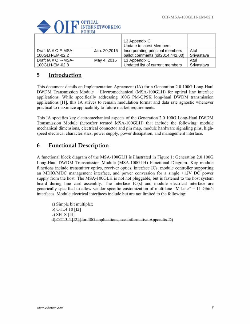
5 Introduction This document details an Implementation Agreement (IA) for a Generation 2.0 100G Long-Haul DWDM Transmission Module – Electromechanical (MSA-100GLH) for optical line interface applications. While specifically addressing 100G PM-QPSK long-haul DWDM transmission applications [I1], this IA strives to remain modulation format and data rate agnostic whenever practical to maximize applicability to future market requirements. This IA specifies key electromechanical aspects of the Generation 2.0 100G Long-Haul DWDM Transmission Module (hereafter termed MSA-100GLH) that include the following: module mechanical dimensions, electrical connector and pin map, module hardware signaling pins, high-speed electrical characteristics, power supply, power dissipation, and management interface. 6 Functional Description A functional block diagram of the MSA-100GLH is illustrated in Figure 1: Generation 2.0 100G Long-Haul DWDM Transmission Module (MSA-100GLH) Functional Diagram. Key module functions include transmitter optics, receiver optics, interface ICs, module controller supporting an MDIO/MDC management interface, and power conversion for a single +12V DC power supply from the host. The MSA-100GLH is not hot pluggable, but is fastened to the host system board during line card assembly. The interface IC(s) and module electrical interface are generically specified to allow vendor specific customization of multilane “M-lane” ~ 11 Gbit/s interfaces. Module electrical interfaces include but are not limited to the following:
a) Simple bit multiplex b) OTL4.10 [I2] c) SFI-S [I3] d) OTL3.4 [I2] (for 40G applications, see informative Appendix D)
www.oi
F
iforum.com
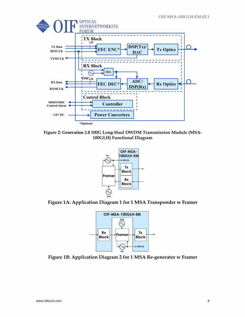
Figure 2: Gen
Figure 1A
Figure 1B
neration 2.0 1
A: Applicati
B: Applicati
OSC
100G Long-H100GLH) Fu
ion Diagram
ion Diagram
Haul DWDMunctional D
m 1 for 1 M
m 2 for 1 M
O
M TransmisDiagram
MSA Transp
MSA Re-gen
OIF-MSA-100
ssion Modu
ponder w F
nerator w F
0GLH-EM-02
ule (MSA-
Framer
Framer
2.1
8
www.oi
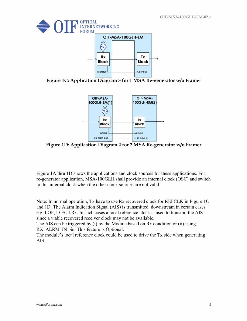
Figurre-geto thi Noteand 1e.g. LsinceThe ARX_AThe mAIS.
iforum.com
Figure 1C:
Figure 1D:
re 1A thru 1Dnerator appl
is internal clo
: In normal o1D. The AlarLOF, LOS at a viable rec
AIS can be trALRM_IN pmodule’s loc
Applicatio
Applicatio
D shows thelication, MSAock when th
operation, Txrm Indicatiot Rx. In suchcovered receriggered by pin. This feacal reference
on Diagram
on Diagram
e applicationA-100GLH
he other clock
x have to uson Signal (AIh cases a lociver clock m(i) by the M
ature is Optioe clock could
m 3 for 1 MS
m 4 for 2 M
s and clock shall providk sources ar
e Rx recoveIS) is transmal reference
may not be avModule based
onal. d be used to
O
SA Re-gen
SA Re-gen
sources for tde an internalre not valid
red clock fomitted down
clock is usevailable. d on Rx cond
drive the Tx
OIF-MSA-100
nerator w/o
nerator w/o
these applical clock (OSC
or REFCLK istream in ce
ed to transmi
dition or (ii)
x side when g
0GLH-EM-02
Framer
Framer
ations. For C) and switc
in Figure 1Certain cases it the AIS
using
generating
2.1
9
ch
C
OIF-MSA-100GLH-EM-02.1
www.oiforum.com 10
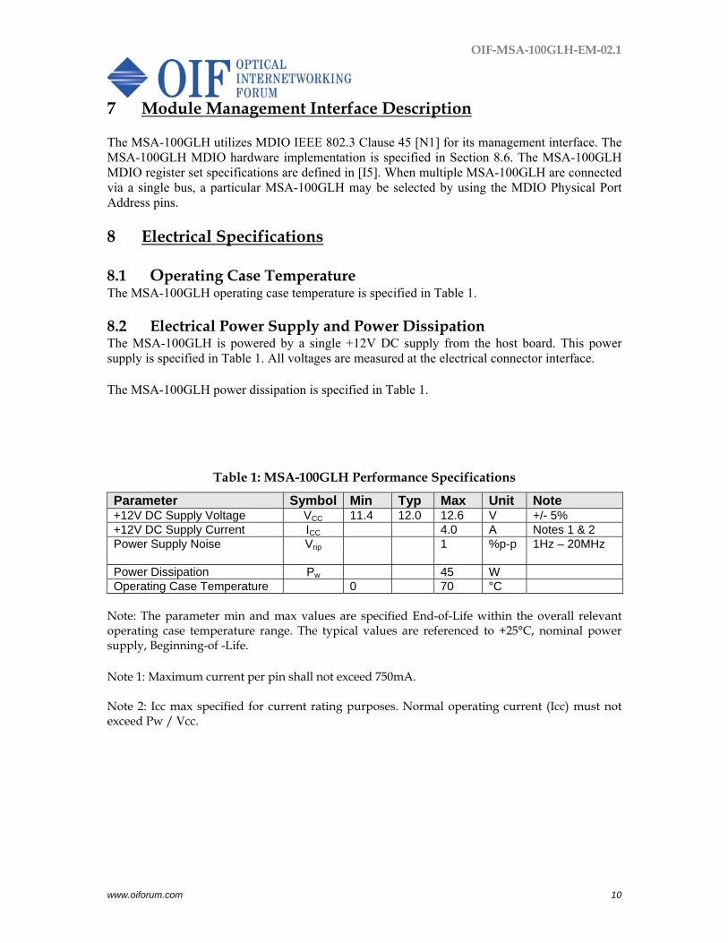
7 Module Management Interface Description The MSA-100GLH utilizes MDIO IEEE 802.3 Clause 45 [N1] for its management interface. The MSA-100GLH MDIO hardware implementation is specified in Section 8.6. The MSA-100GLH MDIO register set specifications are defined in [I5]. When multiple MSA-100GLH are connected via a single bus, a particular MSA-100GLH may be selected by using the MDIO Physical Port Address pins. 8 Electrical Specifications 8.1 Operating Case Temperature The MSA-100GLH operating case temperature is specified in Table 1. 8.2 Electrical Power Supply and Power Dissipation The MSA-100GLH is powered by a single +12V DC supply from the host board. This power supply is specified in Table 1. All voltages are measured at the electrical connector interface. The MSA-100GLH power dissipation is specified in Table 1.
Table 1: MSA-100GLH Performance Specifications
Parameter Symbol Min Typ Max Unit Note +12V DC Supply Voltage VCC 11.4 12.0 12.6 V +/- 5% +12V DC Supply Current ICC 4.0 A Notes 1 & 2 Power Supply Noise Vrip 1
%p-p 1Hz – 20MHz
Power Dissipation Pw 45 W Operating Case Temperature 0 70 °C
Note: The parameter min and max values are specified End-of-Life within the overall relevant operating case temperature range. The typical values are referenced to +25°C, nominal power supply, Beginning-of -Life. Note 1: Maximum current per pin shall not exceed 750mA. Note 2: Icc max specified for current rating purposes. Normal operating current (Icc) must not exceed Pw / Vcc.
OIF-MSA-100GLH-EM-02.1
www.oiforum.com 11
8.3 High Speed Pin Electrical Specifications 8.3.1 Transmitter Data (TX) The Transmitter Data (TX) signals shall comply with CEI-11G-MR Low Swing option as per Clauses 9.3.1. and 9.3.1.2 [N2]. Full Swing support is not required. The recommended termination of the TX pins is given in Figure 3. 8.3.2 Receiver Data (RX) The Receiver Data (RX) signals shall comply with CEI-11G-MR Clause 9.3.3 [N2]. The recommended termination of the RX pins is given in Figure 3. 8.3.3 Reference Clock (REFCLK) The host shall supply a reference clock (REFCLK) at 1/16 of the electrical lane rate. The host shall optionally supply a reference clock (REFCLK) at 1/64 of the electrical lane rate. The REFCLK shall be CML differential AC coupled and terminated with 50 Ohm internal VTT within the MSA-100GLH, as shown in Figure 3. A frequency locked relationship is required between the transmit data lanes (TX/TXDSC) and the reference clock (REFCLK). There is no required phase relationship between the data lanes and the reference clock. The REFCLK frequency shall not deviate from nominal by more than ±20 ppm. Detailed reference clock characteristics for the MSA-100GLH are given in Table 2. When the two MSA client interfaces are connected back-to-back for regenerator application then the two DC blocking capacitors are used in series and this will change the filter cutoff frequency.
www.oi
ParaImpeFreq
FreqStabDiffeVoltClocClocTime
Figur
8.3.4The Mintendprovid
iforum.com
Table
ameter edance
quency
quency ility erential age
ck Duty Cycleck Rise/Fall e
re 3: High S
4 TransmMSA-100GLHded to be useded, the clo
2: MSA-100
Symbol Zd f
Δf
VDIFF
e CDC tr/f
peed I/O for
mitter MonH optionally med as a refereck shall ope
0GLH Refere
Min 80
-20
400
40 200 50
r Data and C
nitor Clockmay supply aence for meaerate at 1/8
ence Clock
Typ Ma100 120
1/16
1/64
+20
160
60 125 315
Clocks
k (TXMCLKa transmitter masurements o
of the trans
O
(REFCLK) C
ax Unit N0 Ω
Od
Oo
0 ppm
0 mV P
% 0 ps 1
5 ps 1
K) monitor clockf the modulesmitter optic
OIF-MSA-100
Characterist
Notes
Of electrical ladefault Of electrical laoptional
Peak-to-Peak
1/64 electrica1/16 electrica
k (TXMCLK)e optical trancal symbol r
0GLH-EM-02
tics
ane rate -
ane rate -
Differential
al lane rate al lane rate
). This clock nsmit signal. rate for 32G
2.1
12
is If
Gb
OIF-MSA-100GLH-EM-02.1
www.oiforum.com 13
applications1. This rate is optimized for triggering high-speed sampling scopes. Clock termination is shown in Figure 3. TXMCLK characteristics are summarized in Table 3. 8.3.5 Receiver Monitor Clock (RXMCLK) The MSA-100GLH optionally may supply a receiver monitor clock (RXMCLK). This clock is intended to be used as a reference for measurements of the module receive data. If provided, the clock shall operate at 1/16 of the receiver electrical lane data rate. The RXMCLK may optionally operate at 1/64 of the receiver electrical lane data rate. Clock termination is shown in Figure 3. RXMCLK characteristics are summarized in Table 3.
Table 3: Optional TXMCLK and RXMCLK Characteristics
Parameter Symbol Min Typ Max Unit Notes Impedance Zd 80 100 120 Ω Frequency - TXMCLK
1/8 Of TX optical symbol rate - default
Frequency - RXMCLK
1/16 Of RX electrical lane data rate - default
1/64 Of RX electrical lane data rate - optional
Output Differential Voltage
VDIFF 400 1600 mV Peak-to-Peak Differential
Clock Duty Cycle CDC 40 60 % 8.4 Control Pins (non-MDIO) Functional Description The control functions between a host and a MSA-100GLH are conducted through a set of dedicated, non-data hardware signal pins on the 168-pin electrical connector and via an MDIO interface. The signal pins work together with the MDIO interface to form a complete HOST/MSA-100GLH management interface. Upon module initialization, the control functions are available. Pins allocated to control functions in the 168-pin electrical connector are listed in Table 4.
1 For 40G applications, other clock rates may be necessary for operating with available test equipment.
OIF-MSA-100GLH-EM-02.1
www.oiforum.com 14
Table 4: MSA-100GLH Control Pins (non-MDIO)
Pin #
Symbol Description I/O
Logic “H” “L” Pull-up /down
B20 PRG_CNTL1 Programmable Control 1 Default: TRXIC_RSTn, TX & RX ICs reset, “0”: reset, “1” or NC: enabled
I 3.3V LVCMOS
Per MDIO document
Pull–Up1
B19 PRG_CNTL2 Programmable Control 2 For Future Use
I 3.3V LVCMOS
Pull–Up1
B18 PRG_CNTL3 Programmable Control 3 For Future Use
I 3.3V LVCMOS
Pull–Up1
B13 PM_SYNC Performance Monitoring Sync Rising edge synchronizes PM statistics counters
I 3.3V LVCMOS
Pull-Down2
B11 TX_DIS Transmitter Disable “0”: transmitter enabled “1” or NC: transmitter disabled
I 3.3V LVCMOS
Disable Enable Pull-Up1
B10 MOD_LOPWR Module Low Power “0”: power-on enabled “1” or NC: module in low power (safe) mode
I 3.3V LVCMOS
Low Power
Enable Pull–Up1
B9 MOD_ RSTn Module Reset “0”: resets the module “1”: module enabled
I 3.3V LVCMOS
Enable Reset Pull-Down2
Note 1: Pull-Up resistor (4.7k - 10kOhm) is located within the MSA-100GLH. Note 2: Pull-Down resistor (4.7k - 10kOhm) is located within the MSA-100GLH. 8.4.1 Programmable Control Pins (PRG_CNTLs) The Programmable Control pins (PRG_CNTL) allow the host to program certain MSA-100GLH control functions via a hardware pin. The intention is to allow for maximum design and debug flexibility. The default setting for Control 1 is control of the Transmit & Receive Reset. Controls 2 and 3 are for future use.
8.4.1.1 Programmable Control 1 Pin (PRG_CNTL1) Programmable Control 1 Pin (PRG_CNTL1) is an input pin from the host, operating with programmable logic. It is pulled up in the MSA-100GLH. It can be re-programmed over MDIO registers to another MDIO control register while the module is in any steady state except Reset. The default function is Transmit & Receive circuitry reset (TRXIC_RSTn) with active-low logic. When TRXIC_RSTn is asserted (driven low), the digital transmit and receive circuitry is reset clearing all FIFOs and/or resetting all CDRs. When de-asserted, the digital transmit and receive circuitry shall resume normal operation.
8.4.1.2 Programmable Control 2 Pin (PRG_CNTL2) Programmable Control 2 Pin (PRG_CNTL2) is an input from the host, operating with programmable logic. It is pulled up in the MSA-100GLH. It can be re-programmed over MDIO registers to another MDIO control register while the module is in any steady state except Reset. It is reserved for future use.
8.4.1.3 Programmable Control 3 Pin (PRG_CNTL3)
www.oi
Progrprogrregistis rese
8.4.1The PpurposynchperforPM_S
8.4.1The TThis pinsideshall specift_on a
8.4.1The Mhigh 100Gassert In LoWhile The t_MOIA.
iforum.com
rammable Coammable logters to anothererved for futu
.4 PerforPerformance ose of this pinhronizing mormance monitSYNC is optio
.5 TransmTransmitter Dpin is pulled e a MSA-100be switched ofication. The are applicatio
Fi
.6 ModuModule Low logic. It is puLH shall be ted. When de-
w Power mode the module
timing diagrOD_LOPWR_
ontrol 3 Pinic. It is puller MDIO contr
ure use.
rmance MoMonitoring S
n is to providodule-level toring data coonal for the M
mitter Disaisable pin (TXup in the MS
0GLH shall bon accordingtiming diagran specific and
igure 4: Tran
ule Low PowPower pin (Mulled up in tin the low p
-asserted, the
de, the MSA-is in Low Pow
ram for the_on and t_ MO
n (PRG_CNTd up in the Mrol register w
nitoring SySynchronizatide a synchron
performance ollection. TheMSA-100GLH
able Pin (TXX_DIS) is an SA-100GLH. be switched o
to a predefinam for TX_Dd not specifie
nsmitter Dis
wer Pin (MOMOD_LOPWthe MSA-100power state a
MSA-100GL
-100GLH shawer mode, it h
MOD_LOPOD_LOPWR
TL3) is an MSA-100GLHwhile the modu
ynchronization pin (PM_ization pulse
monitoringe default timeH.
X_DIS) input from thWhen TX_D
off. When thisned TX powe
DIS pin is illued in this IA.
sable (TX_D
OD_LOPWWR) is an inp0GLH. Whenand will stay LH shall initia
ll communicahas a maximu
PWR pin is R_off are appl
O
input from H. It can be rule is in any s
tion (PM_SY_SYNC) is an
from the hosg data collee period of thi
he host, operaDIS is assertes pin is de-aser-on processustrated in Fig
DIS) Timing
WR) put from the hn MOD_LOP
in the low pate the High-P
ate via the MDum power con
illustrated lication speci
OIF-MSA-100
the host, ore-programmesteady state e
YNC) n input fromst time refereection with is signal is 1 s
ating with acted, all of the osserted, optic defined by m
gure 4. Value
g Diagram
host, operatinWR is assert
power state aPower-Up pro
DIO managemnsumption of
in Figure 5ific and not sp
0GLH-EM-02
operating wited over MDIexcept Reset.
m the host. Thence source fo
host systemsecond. Use o
tive-high logioptical outpu
cal transmittermodule vendoes for t_off an
ng with activeted, the MSA
as long as it ocess.
ment interfacf 6W.
5. Values fopecified in th
2.1
15
th O It
he or m of
c. uts rs or nd
e-A-is
e.
or his
www.oi
8.4.1The MThis pMSAand sh 8.5 Alarmnon-dThe smanagPins a
iforum.com
Figur
.7 ModuModule Resetpin is pulled -100GLH enthall begin an
Alarm P
m indications data hardwareignal pins wogement interfallocated to al
re 5: Module
ule Reset Pint pin (MOD_down in the
ters the Resetinitialization
Pins (non-M
from the MSe signal pins ork together wface. Upon mlarm function
e Low Powe
n (MOD_RSRSTn) is an MSA-100GL
t state. Whenprocess as pa
MDIO) Fu
SA-100GLH ton the 168-p
with the MDIOmodule initialns in the 168-p
er (MOD_LO
STn) input from thLH. When Mn de-asserted, art of the over
unctional D
to the host arpin electrical O interface toization, the apin electrical
O
OPWR) Tim
he host, operaMOD_RSTn is
the MSA-10rall module st
Descriptio
re conducted connector an
o form a compalarm indicaticonnector are
OIF-MSA-100
ming Diagram
ating with acts asserted (dr
00GLH exits tart-up sequen
on
through a send via an Mplete HOST/Mion functionse listed in Tab
0GLH-EM-02
m
tive-low logiriven low), ththe Reset statnce.
et of dedicatedDIO interfacMSA-100GLs are availablble 5.
2.1
16
c. he te
d, e. H e.
OIF-MSA-100GLH-EM-02.1
www.oiforum.com 17
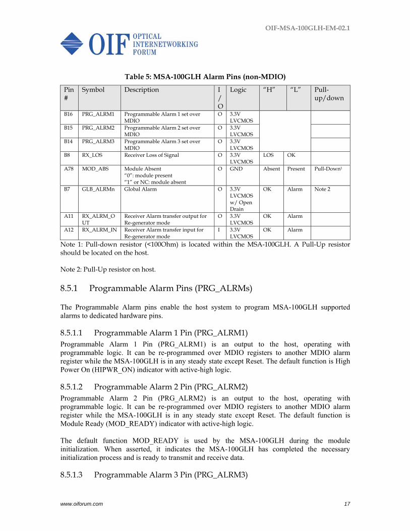
Table 5: MSA-100GLH Alarm Pins (non-MDIO)
Pin #
Symbol Description I/O
Logic “H” “L” Pull-up/down
B16 PRG_ALRM1 Programmable Alarm 1 set over MDIO
O 3.3V LVCMOS
B15 PRG_ALRM2 Programmable Alarm 2 set over MDIO
O 3.3V LVCMOS
B14 PRG_ALRM3 Programmable Alarm 3 set over MDIO
O 3.3V LVCMOS
B8 RX_LOS Receiver Loss of Signal O 3.3V LVCMOS
LOS OK
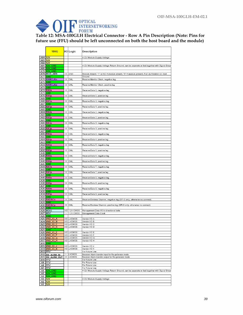
A78 MOD_ABS Module Absent “0”: module present “1” or NC: module absent
O GND Absent Present Pull-Down1
B7 GLB_ALRMn Global Alarm O 3.3V LVCMOS w/ Open Drain
OK Alarm Note 2
A11 RX_ALRM_OUT
Receiver Alarm transfer output for Re-generator mode
O 3.3V LVCMOS
OK Alarm
A12 RX_ALRM_IN Receiver Alarm transfer input for Re-generator mode
I 3.3V LVCMOS
OK Alarm
Note 1: Pull-down resistor (<100Ohm) is located within the MSA-100GLH. A Pull-Up resistor should be located on the host. Note 2: Pull-Up resistor on host. 8.5.1 Programmable Alarm Pins (PRG_ALRMs) The Programmable Alarm pins enable the host system to program MSA-100GLH supported alarms to dedicated hardware pins.
8.5.1.1 Programmable Alarm 1 Pin (PRG_ALRM1) Programmable Alarm 1 Pin (PRG_ALRM1) is an output to the host, operating with programmable logic. It can be re-programmed over MDIO registers to another MDIO alarm register while the MSA-100GLH is in any steady state except Reset. The default function is High Power On (HIPWR_ON) indicator with active-high logic.
8.5.1.2 Programmable Alarm 2 Pin (PRG_ALRM2) Programmable Alarm 2 Pin (PRG_ALRM2) is an output to the host, operating with programmable logic. It can be re-programmed over MDIO registers to another MDIO alarm register while the MSA-100GLH is in any steady state except Reset. The default function is Module Ready (MOD_READY) indicator with active-high logic. The default function MOD_READY is used by the MSA-100GLH during the module initialization. When asserted, it indicates the MSA-100GLH has completed the necessary initialization process and is ready to transmit and receive data.
8.5.1.3 Programmable Alarm 3 Pin (PRG_ALRM3)

www.oi
ProgrprogrregistModu The dWhen 8.5.2 The Rlogic.expecspecifillustrspecif
8.5.3 The Mpulledassertassert 8.5.4 The GWhen(FAWstatusALRMis recoresponidentireadin(drive
iforum.com
rammable Alammable logter while the ule Fault (MO
default function asserted, it i
2 Receiv
Receiver Loss When assert
cted value. Tfied by the hrated in Figufied in this IA
Figu
3 Modul
Module Absed up on the hts a “Low” coted “High” wh
4 Global
Global Alarmn GLB_ALRM
WS) conditions conditions lMn may be pommended thnd to the asifies the sourng action cleaen high) the G
larm 3 Pin gic. It can be
MSA-100GLOD_FAULT)
on MOD_FAndicates the M
er Loss of
s of Signal pited, it indicat
The optical phost system oure 6. ValuesA.
ure 6: Receiv
le Absent P
ent (MOD_Ahost board anondition whenhen the MSA
Alarm Pin
m pin (GLB_AMn is assert
n has occurrelatched in theprogrammed that the host bossertion of thce of the fauars the latche
GLB_ALRMn
(PRG_ALRe re-programmLH is in anyindicator with
AULT is usedMSA-100GLH
Signal Pin
in (RX_LOS)tes received oower at whicor module ves for t_loss_o
ver Loss of S
Pin (MOD_
ABS) pin is and is pulled n the MSA-1
A-100GLH is p
n (GLB_AL
ALRMn) is aned (driven lod. It is driven
e latched regito assert onlyoard be desighis pin. Uponult by readinged registers, wn pin.
RM3) is an med over M
y steady stateh active-high
d by the MSAH has entered
n (RX_LOS
) is an outputoptical powerch RX_LOS endor. The tion and t_ lo
Signal (RX_
_ABS)
an output fromdown to gro00GLH is pluphysically ab
LRMn)
n output to thow), it indican by the logiisters. Maskin
y for specific gned to supporn the assertio
g the latched which in turn
O
output to MDIO register
e except Reslogic.
A-100GLH dud into a fault s
S)
ut to the host,r in the MSA
is asserted iming diagra
oss_off are ap
_LOS) Timin
m the MSA-ound in the Mlugged into a sent from a h
he host, operaates that a Fical OR of alng Registers fault/alarm/wrt high-prioriton of this pregisters ove
n causes the M
OIF-MSA-100
the host, ors to anotherset. The defau
uring modulestate.
operating wA-100GLH is
is applicationam for the RXpplication sp
ng Diagram
-100GLH to MSA-100GLH
host socket. host socket.
ating with acFault/Alarm/Wll fault, alarmare provided
warning/statusty event hand
pin, the host er the MDIO MSA-100GL
0GLH-EM-02
operating witr MDIO alarmult function
e initialization
with active-higlower than thn specific anX_LOS pin
pecific and no
m
the host. It H. MOD_ABMOD_ABS
tive-low logiWarning/Statum, warning and so that GLBs conditions. dling service t
event handleinterface. Th
LH to de-asse
2.1
18
th m is
n.
gh he nd is ot
is BS
is
ic. us nd B-It to er he ert
www.oi
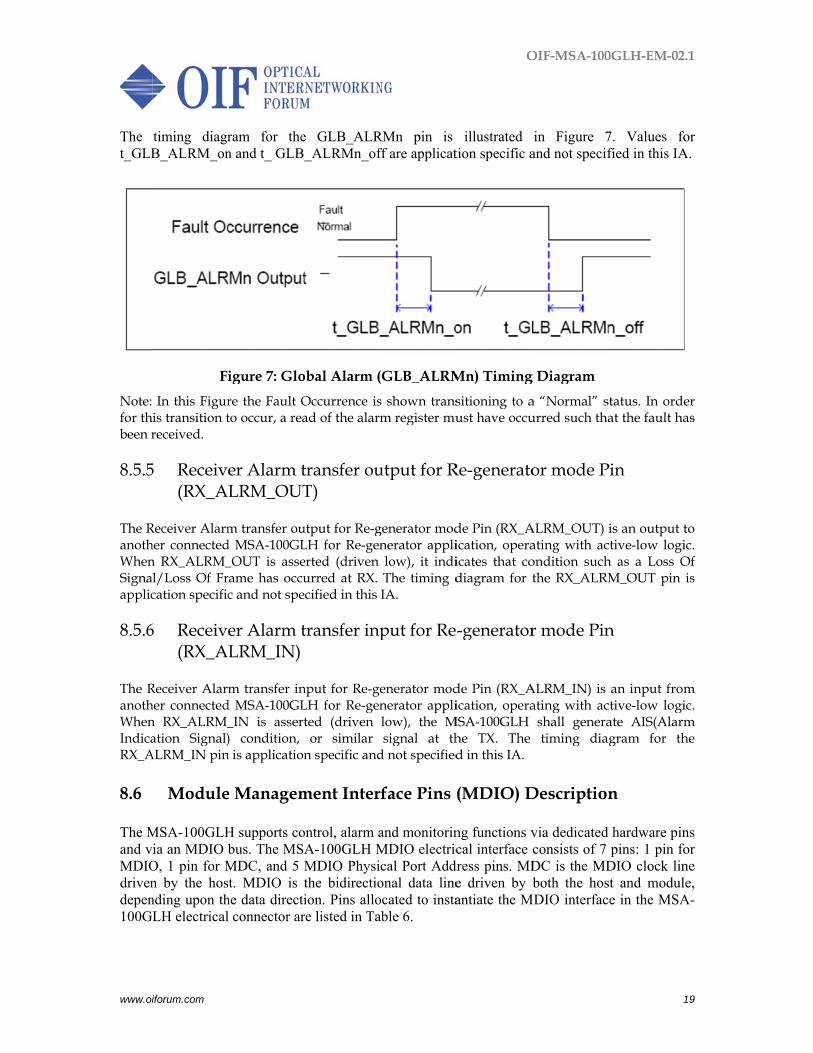
The t_GLB
Note:for thbeen r 8.5.5
The RanothWhenSignaapplic 8.5.6
The RanothWhenIndicaRX_A 8.6 The Mand vMDIOdrivendepen100G
iforum.com
timing diagrB_ALRM_on
Fi In this Figur
his transition treceived.
5 Receiv(RX_A
Receiver Alarmher connectedn RX_ALRM_l/Loss Of Frcation specific
6 Receiv(RX_A
Receiver Alarher connectedn RX_ALRM_ation Signal)
ALRM_IN pin
Module
MSA-100GLHvia an MDIO bO, 1 pin for Mn by the hosnding upon thLH electrical
ram for then and t_ GLB
igure 7: Glore the Fault Oto occur, a rea
er Alarm tLRM_OUT
m transfer oud MSA-100GL_OUT is asserame has occuc and not spe
er Alarm tLRM_IN)
m transfer ind MSA-100GL_IN is assert) condition,
n is application
e Managem
H supports cobus. The MSAMDC, and 5 t. MDIO is t
he data directil connector ar
e GLB_ALR_ALRMn_of
obal Alarm (Occurrence isad of the alarm
transfer ouT)
utput for Re-gLH for Re-generted (driven urred at RX.
ecified in this
transfer inp
nput for Re-geLH for Re-gented (driven or similar
n specific and
ment Inter
ontrol, alarm aA-100GLH MMDIO Physithe bidirectioion. Pins allore listed in Ta
RMn pin is ff are applicat
(GLB_ALRMs shown transm register mu
utput for R
generator modnerator appli low), it indi The timing dIA.
put for Re
enerator modnerator applilow), the Msignal at th
d not specified
rface Pins
and monitorinMDIO electriccal Port Addonal data lineocated to instaable 6.
O
illustrated tion specific a
Mn) Timingsitioning to aust have occu
Re-generato
de Pin (RX_Aication, operaicates that codiagram for t
-generator
de Pin (RX_Aication, opera
MSA-100GLH he TX. The d in this IA.
(MDIO) D
ng functions vcal interface
dress pins. MDe driven by bantiate the M
OIF-MSA-100
in Figure 7and not specif
g Diagram a “Normal” surred such tha
or mode P
ALRM_OUT) ating with acondition suchthe RX_ALRM
r mode Pin
ALRM_IN) is ating with ac
shall genera timing dia
Description
via dedicated consists of 7 DC is the MDboth the hos
MDIO interfac
0GLH-EM-02
7. Values fofied in this IA
status. In ordeat the fault ha
Pin
is an output tctive-low logih as a Loss OM_OUT pin
n
an input fromctive-low logiate AIS(Alarmgram for th
n
hardware pinpins: 1 pin fo
DIO clock linst and modulce in the MSA
2.1
19
or A.
er as
to ic. Of is
m ic. m he
ns or ne le, A-

OIF-MSA-100GLH-EM-02.1
www.oiforum.com 20
Table 6: MSA-100GLH MDIO Management Interface Pins
Pin #
Symbol Description I/O
Logic “H” “L” Pull-up /down
A28 MDIO Management Data I/O bi-directional I/O
1.2V LVCMOS
A27 MDC MDIO Clock I 1.2V LVCMOS
B21 PRTADR0 MDIO Physical Port Address bit 0 I 1.2V LVCMOS
B22 PRTADR1 MDIO Physical Port Address bit 1 I 1.2V LVCMOS
B23 PRTADR2 MDIO Physical Port Address bit 2 I 1.2V LVCMOS
B24 PRTADR3 MDIO Physical Port Address bit 3 I 1.2V LVCMOS
B25 PRTADR4 MDIO Physical Port Address bit 3 I 1.2V LVCMOS
8.6.1 Management Data Input/Output Pin (MDIO) The MDIO specification is defined in IEEE 802.3 Clause 45 [N1]. The MSA-100GLH shall support 4.0 Mbit/s maximum data rate. The MSA-100GLH uses an MDIO with 1.2V LVCMOS logic. 8.6.2 Management Data Clock Pin (MDC) The host specifies a maximum MDC rate of 4.0 MHz and MSA-100GLH hence shall support a maximum MDC rate up to 4.0 MHz. The timing diagram for the MDIO and MDC pins is illustrated in Figure 8: Module MDIO & MDC Timing Diagram
The MSA-100GLH shall support a minimal setup (tsetup) and hold (thold) time in its MDIO implementation (see Table 9).

OIF-MSA-100GLH-EM-02.1
www.oiforum.com 21
Figure 8: Module MDIO & MDC Timing Diagram
Note: Measured at Module MDIO & MDC pins. 8.6.3 MDIO Physical Port Address Pins (PRTADRs) The MDIO Physical Port Address pins (PRTADRs) are used by the host system to address all of the MSA-100GLHs contained within its management domain. PRTADR0 corresponds to the LSB in the physical port addressing scheme. The 5-pin Physical Port Address lines are driven by the host to set the module Physical Port Address which should match the address specified in the MDIO Frame. It is recommended that the Physical Port Addresses not be changed while the MSA-100GLH is powered on. 8.7 Hardware Signaling Pin Electrical Specifications 8.7.1 Control & Alarm Pins: 3.3V LVCMOS Electrical Characteristics The hardware control and alarm pins specified as 3.3V LVCMOS functionality described above shall meet the electrical characteristics described in Table 7. Figure 9 illustrates the recommended reference pin input and output terminations.
Table 7: 3.3V LVCMOS Electrical Characteristics
Parameter Symbol Min Typ Max Unit Supply Voltage VCC 3.2 3.3 3.4 V Input High Voltage VIH 2 - VCC+0.3 V Input Low Voltage VIL -0.3 - 0.8 V Input Leakage Current IIN -10 - +10 µA Output High Voltage (IOH=-100 µA) VOH VCC-0.2 - - V Output Low Voltage (IOL= 100 µA) VOL - - 0.2 V

www.oi
8.7.2 The Melectrpin in
ParInpInpInpOutOutOutOutInp
iforum.com
Figur
2 MDIO
MDIO pins rical characternput and outpu
rameter put High Voltaput Low Voltaput Leakage Ctput High Votput Low Voltput High Cutput Low Cur
put Capacitan
re 9: Referen
Interface P
specified as ristics describut termination
Table 8: 1
age age Current oltage ltage
urrent rrent ce
nce +3.3V LV
Pins: 1.2V
1.2V LVCMbed in Table ns.
1.2V LVCM
SymVVI
VVII
VCMOS Inp
LVCMOS
MOS functio8. Figure 9
OS Electrica
mbol MVIH 0VIL -0IIN -1
VOH 1VOL -0OH IOL +Ci
O
put/Output T
Electrical
onality descri9 illustrates t
al Character
Min Ty.84 -0.3 -100 -1.0 -0.3 -- -
+4 -- -
OIF-MSA-100
Termination
Character
ibed above sthe recommen
ristics
yp Max- 1.5 - 0.36- +100- 1.5 - 0.2 - -4 - - - 10
0GLH-EM-02
2
ns
ristics
shall meet thnded referenc
x Unit V 6 V 0 µA V V
mA mA
pF
2.1
22
he ce
www.oi
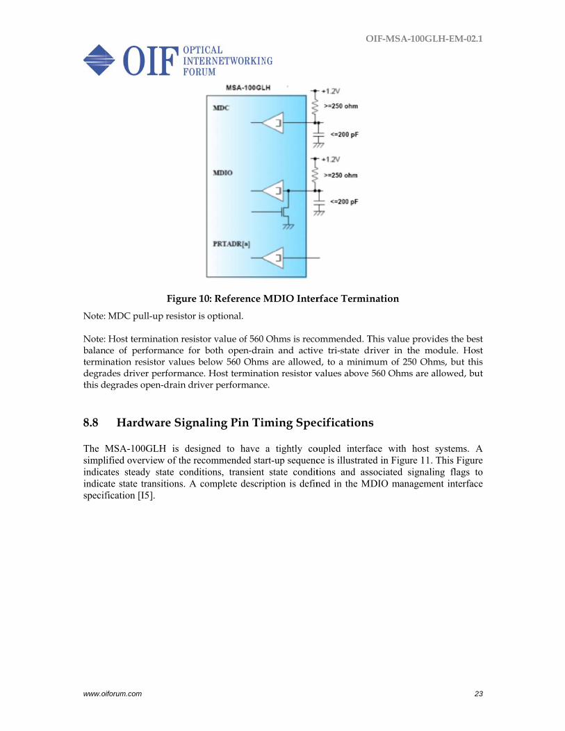
Note: Note:balantermindegrathis d 8.8 The Msimplindicaindicaspecif
iforum.com
MDC pull-up
Host terminace of performnation resisto
ades driver pedegrades open
Hardwa
MSA-100GLified overviewates steady sate state transfication [I5].
Figure 10:p resistor is o
ation resistor mance for boor values beloerformance. Hn-drain driver
are Signali
LH is designw of the recomstate conditiositions. A com
Reference Moptional.
value of 560 oth open-draow 560 OhmHost terminatr performance
ing Pin Ti
ed to have mmended sta
ons, transient mplete descri
MDIO Inter
Ohms is recoain and activ
ms are allowedtion resistor ve.
ming Spec
a tightly coart-up sequenc
state conditiption is defin
O
rface Termin
ommended. Tve tri-state drd, to a minimvalues above
cifications
oupled interface is illustratetions and assned in the M
OIF-MSA-100
nation
This value proriver in the
mum of 250 O 560 Ohms ar
s
ace with hosed in Figure 1sociated sign
MDIO manage
0GLH-EM-02
2
ovides the bemodule. Ho
Ohms, but thre allowed, bu
st systems. A11. This Figurnaling flags tement interfac
2.1
23
est ost his ut
A re to ce
OIF-MSA-100GLH-EM-02.1
www.oiforum.com 24
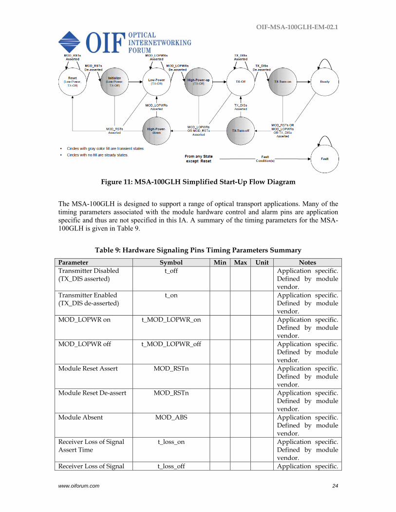
Figure 11: MSA-100GLH Simplified Start-Up Flow Diagram
The MSA-100GLH is designed to support a range of optical transport applications. Many of the timing parameters associated with the module hardware control and alarm pins are application specific and thus are not specified in this IA. A summary of the timing parameters for the MSA-100GLH is given in Table 9.
Table 9: Hardware Signaling Pins Timing Parameters Summary
Parameter Symbol Min Max Unit Notes Transmitter Disabled (TX_DIS asserted)
t_off Application specific. Defined by module vendor.
Transmitter Enabled (TX_DIS de-asserted)
t_on Application specific. Defined by module vendor.
MOD_LOPWR on t_MOD_LOPWR_on Application specific. Defined by module vendor.
MOD_LOPWR off t_MOD_LOPWR_off Application specific. Defined by module vendor.
Module Reset Assert MOD_RSTn Application specific. Defined by module vendor.
Module Reset De-assert MOD_RSTn Application specific. Defined by module vendor.
Module Absent MOD_ABS Application specific. Defined by module vendor.
Receiver Loss of Signal Assert Time
t_loss_on Application specific. Defined by module vendor.
Receiver Loss of Signal t_loss_off Application specific.

OIF-MSA-100GLH-EM-02.1
www.oiforum.com 25
De-assert Time Defined by module vendor.
Global Alarm Assert Delay Time
t_GLB_ALRMn_on This is a logical “OR” of associated MDIO alarm & status registers. See MDIO spec for details.
Global Alarm De-assert Delay Time
t_GLB_ALRMn_off This is a logical “OR” of associated MDIO alarm & status registers. See MDIO spec for details.
Management Interface Clock Period
tprd 250 ns MDC is 4 MHz rate; duty cycle = 50% ± 10% (typ.)
Host MDIO setup time tsetup 10 ns Host MDIO hold time thold 10 ns Module MDIO delay time
tdelay 175 ns
Performance Monitoring Synchronization (PM_SYNC) (optional)
Default period=1 sec. ; min high/low time = 100msec.
9 Mechanical Specifications 9.1 Mechanical Overview The MSA-100GLH is designed to be assembled into a host system line card. The MSA-100GLH is electrically connected to the host line card by a 168 position connector specified herein and is physically fastened to the host line card by mounting screws through the host line card PCB. The MSA-100GLH supports two optical fiber pigtails, one for optical transmit and one for optical receive. These optical fiber pigtails are terminated and attached to host line card face plate. The MSA-100GLH is not designed to be hot-pluggable. Its power and initialization sequencing in the host line card are specified by the host line card and transponder vendors. 9.2 Electrical Connector The Hirose FX10A-168P/S-SV(83) connector assembly [N3] is specified for the host line card – MSA-100GLH electrical connector. This connector is a two component (header, receptacle), 168 position, board mounted style assembly. It meets CEI-11G-MR [N2] signal integrity performance and provides 4mm - 8mm mated stack height flexibility by header component changes only, i.e. the MSA-100GLH receptacle component remains fixed. Detailed mechanical specifications and layout design application notes may be found at [N3]. The Hirose FX10B-168P/S-SV(83) connector assembly [N3] is also specified as an option for the host line card – MSA-100GLH electrical connector. The FX10A connector style has guidepost
www.oi
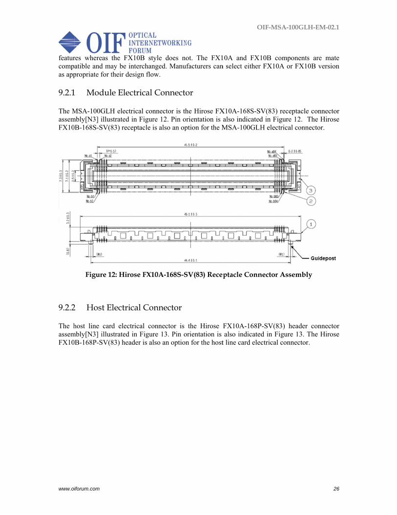
featurcompas app 9.2.1 The MassemFX10
9.2.2 The hassemFX10
iforum.com
res whereas atible and mapropriate for t
1 Modul
MSA-100GLHmbly[N3] illus0B-168S-SV(8
Figure 1
2 Host E
host line carmbly[N3] illus0B-168P-SV(8
the FX10B ay be interchtheir design fl
le Electrica
H electrical cstrated in Fig83) receptacle
2: Hirose FX
lectrical C
d electrical cstrated in Fig83) header is
style does nanged. Manu
flow.
al Connecto
connector is thure 12. Pin oe is also an op
X10A-168S-S
Connector
connector is gure 13. Pin oalso an option
ot. The FX1
ufacturers can
or
he Hirose FXorientation is ption for the M
SV(83) Rece
the Hirose Forientation is n for the host
O
10A and FXn select either
X10A-168S-Salso indicatedMSA-100GLH
ptacle Conn
FX10A-168Palso indicate
t line card ele
OIF-MSA-100
10B componr FX10A or F
SV(83) receptd in Figure 1H electrical c
nector Assem
P-SV(83) heaed in Figure 1ectrical conne
0GLH-EM-02
2
nents are matFX10B versio
tacle connecto2. The Hiros
connector.
mbly
ader connecto13. The Hirosctor.
2.1
26
te on
or se
or se
www.oi
9.2.3 For athe mbetwe
to ass
this m14. M
iforum.com
Figure
3 Host-M
lignment of hmaximum alloeen the conne
ure CN matin
may cause conMaximum allo
e 13: Hirose F
Module Co
host – MSA owable misactor guide pin
ng after insert
nnector and cwable misalig
2
G Maximum−GHφ
2
G Maximum−GHφ
FX10A-168P
onnector A
100GLH conalignment valn (GP) and th
ting guide pin
contact deformgnment shoul
Ma2
Gap
≤−
=GPφ
Ma2
Gap
≥−=
GPφ
P-SV(83) Hea
Alignment
nnector matinlue of the co
he PCB guide
ns into the gui
mation. Tolerld be ≤0.42mm
misa aximum
misa aximum
O
ader Conne
ng, misalignmonnector (CNpin hole (GH
ide pin hole. I
rance of GP am for FX10.
ofnt alignme
ofnt alignme
OIF-MSA-100
ctor Assemb
ment should bN) mating. MH) is:
If
and GH is def
CN thef
CN thef
0GLH-EM-02
2
bly
be smaller thMaximum ga
fined in Figur
2.1
27
at ap
re
OIF-MSA-100GLH-EM-02.1
www.oiforum.com 28
Figure 14: FX10 Connector Alignment
9.3 Module Dimensions Two options are specified for the MSA-100GLH mechanical dimensions:
1) Flattop 2) Integrated Heat Sink
The flattop option is specified to allow customization of the MSA-100GLH bolt-on heat sink for supporting a wide array of optical transport applications. With this option, the bolt-on heat sink is specified by the host system designer, allowing maximum flexibility in their system design while maintaining a common module form factor. The integrated heat sink option is specified to simplify the host system design and supports module thermal performance per the maximum power consumption specified in Section 8.2. Mechanical dimensions of the MSA-100GLH with non-conductive sheet are specified in Figure 15. If a non-conductive sheet is used, the thickness is specified as 0.15 +/- 0.05mm.
Maximum Gap should be
Maximum allowable misalignment of the FX10
αφ ±GP
βφ ±GH
χ±pitchpin Guide
δ±pitch holepin Guide
ε±accuracy mounting CN
ϕ±accuracy mounting CN
αφ ±GP
βφ ±GH
χ±pitchpin Guide
δ±pitch holepin Guide
ε±accuracy mounting CN
ϕ±accuracy mounting CN
( ) ( ) ϕεδχαφβφ+++≥
+−=
2GP-GH
Gap Maximum
( )( )
22
2GP-GH
2GPGHβαϕεδχφφβαϕεδχφφ
++×+++≥
++×++++≥
( ) CN theofnt misalignme Maximum2
2≤
++×+++ βαϕεδχ
( ) 03.02
2≤
++×+++ βαϕεδχ [mm] 0.42
OIF-MSA-100GLH-EM-02.1
www.oiforum.com 29
Figure 15: MSA-100GLH Non-conductive Sheet Dimensions
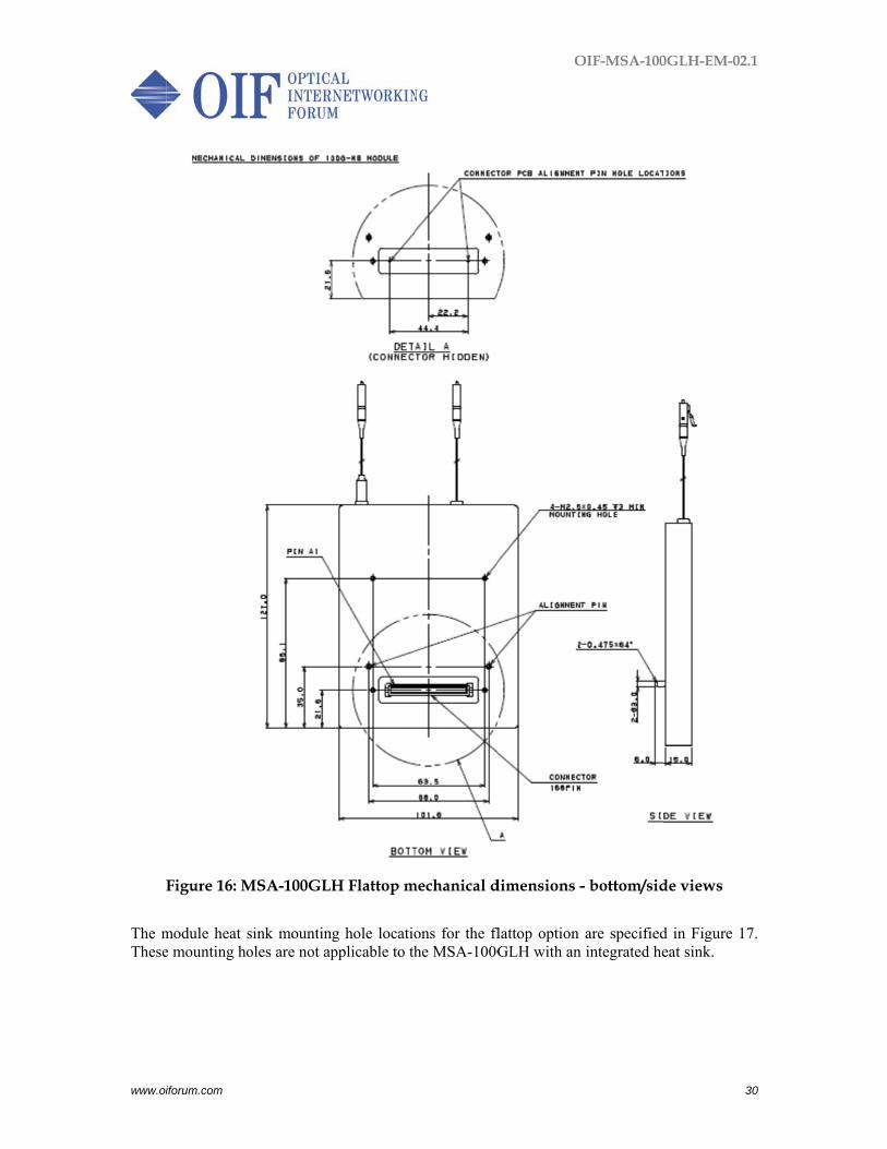
Note: The module vendor must ensure the module connector receptacle component is placed to enable the module to properly mate with the host connector header when the minimum height header component (i.e. C=4mm) is used by the host. 9.3.1 Flattop Mechanical dimensions of the MSA-100GLH flattop module are specified in Figure 16. The maximum module size is specified as: 101.6mm x 127.0mm (4” x 5”) Figure 16 also specifies the receptacle connector position, connector guide pin locations and module mounting hole locations.
Module and Host PCB dimensions and tolerances in mm.
MSA Module PCB
Host PCB
Header Recept.
Sheet Thickness : S +/- s Module base: B +/- b Conn. stacking height: C +/- c Solder paste thickness: P +/- p
MSA Module
B P
S C
www.oi
The mThese
iforum.com
Figure 16: M
module heat se mounting ho
MSA-100GLH
sink mountinoles are not ap
H Flattop m
g hole locatiopplicable to th
mechanical d
ons for the flhe MSA-100G
O
dimensions -
lattop option GLH with an
OIF-MSA-100
- bottom/sid
are specifiedn integrated he
0GLH-EM-02
3
de views
d in Figure 17eat sink.
2.1
30
7.
OIF-MSA-100GLH-EM-02.1
www.oiforum.com 31
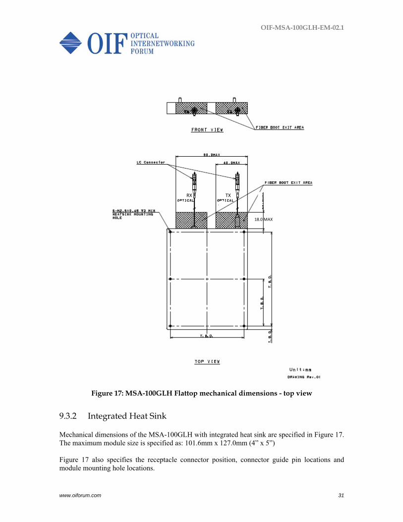
Figure 17: MSA-100GLH Flattop mechanical dimensions - top view
9.3.2 Integrated Heat Sink Mechanical dimensions of the MSA-100GLH with integrated heat sink are specified in Figure 17. The maximum module size is specified as: 101.6mm x 127.0mm (4” x 5”) Figure 17 also specifies the receptacle connector position, connector guide pin locations and module mounting hole locations.
RX TX
18.0 MAX
www.oi
F
The torientHoweFigur
iforum.com
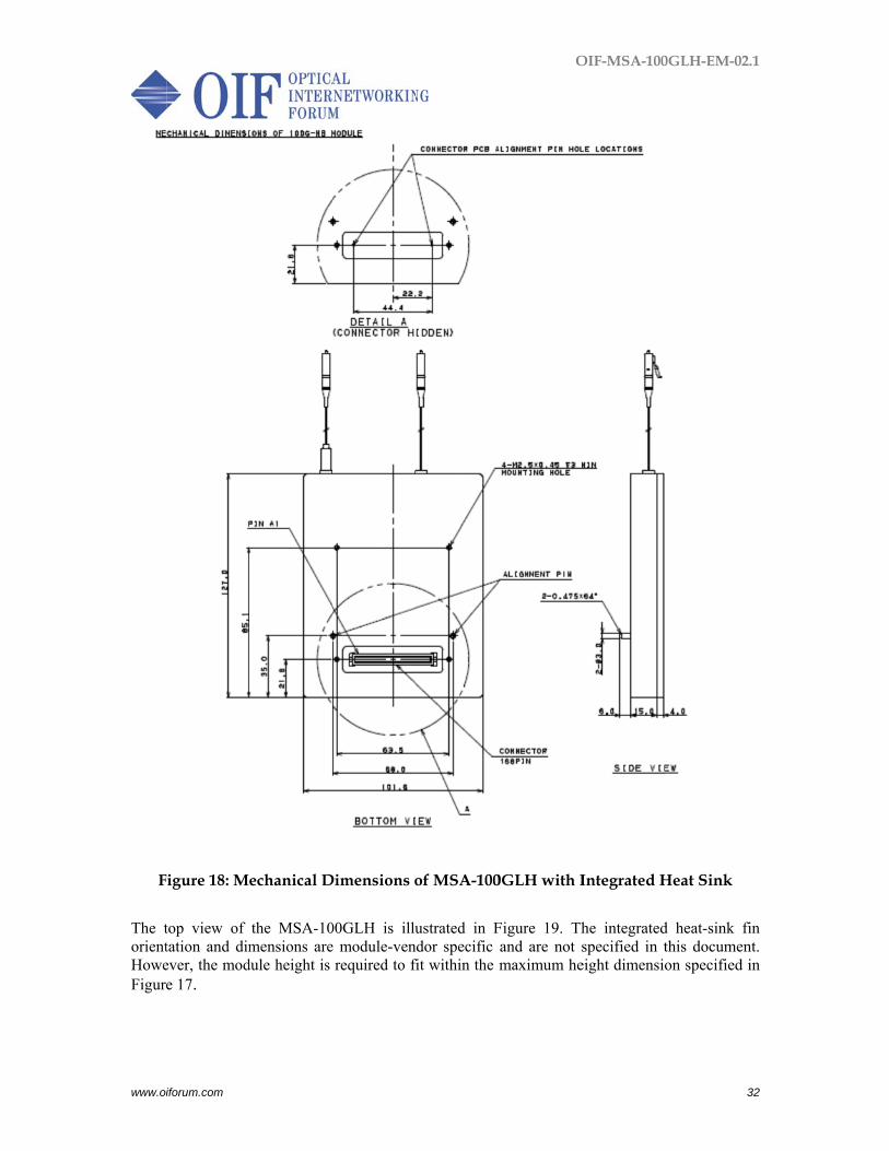
Figure 18: M
top view of tation and dimever, the mode 17.
echanical D
the MSA-10mensions are
dule height is
Dimensions o
00GLH is illue module-ven
required to f
of MSA-100
ustrated in Fndor specific fit within the m
O
0GLH with I
Figure 19. Thand are not smaximum he
OIF-MSA-100
Integrated H
he integratedspecified in t
eight dimensio
0GLH-EM-02
3
Heat Sink
d heat-sink fithis documenon specified i
2.1
32
fin nt. in
OIF-MSA-100GLH-EM-02.1
www.oiforum.com 33
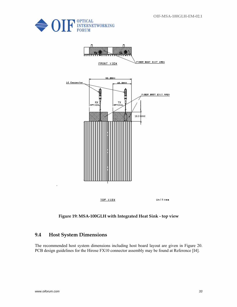
Figure 19: MSA-100GLH with Integrated Heat Sink - top view
9.4 Host System Dimensions The recommended host system dimensions including host board layout are given in Figure 20. PCB design guidelines for the Hirose FX10 connector assembly may be found at Reference [I4].
RX TX
18.0 MAX
OIF-MSA-100GLH-EM-02.1
www.oiforum.com 34
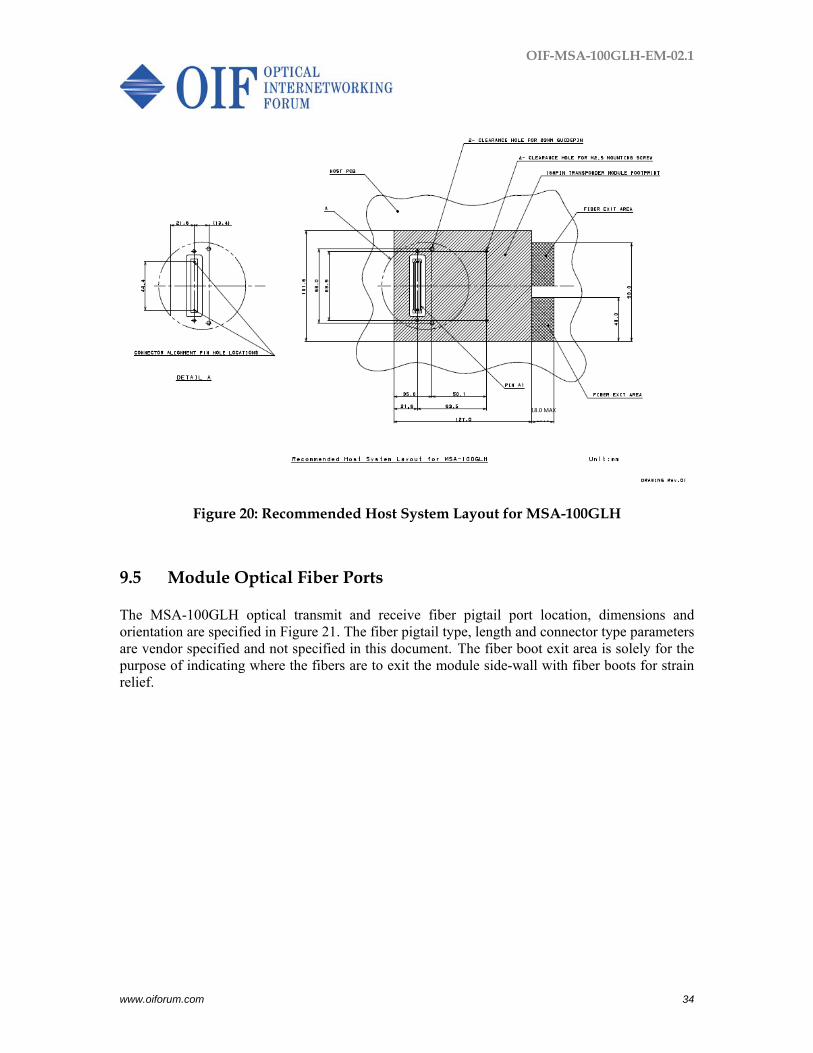
Figure 20: Recommended Host System Layout for MSA-100GLH
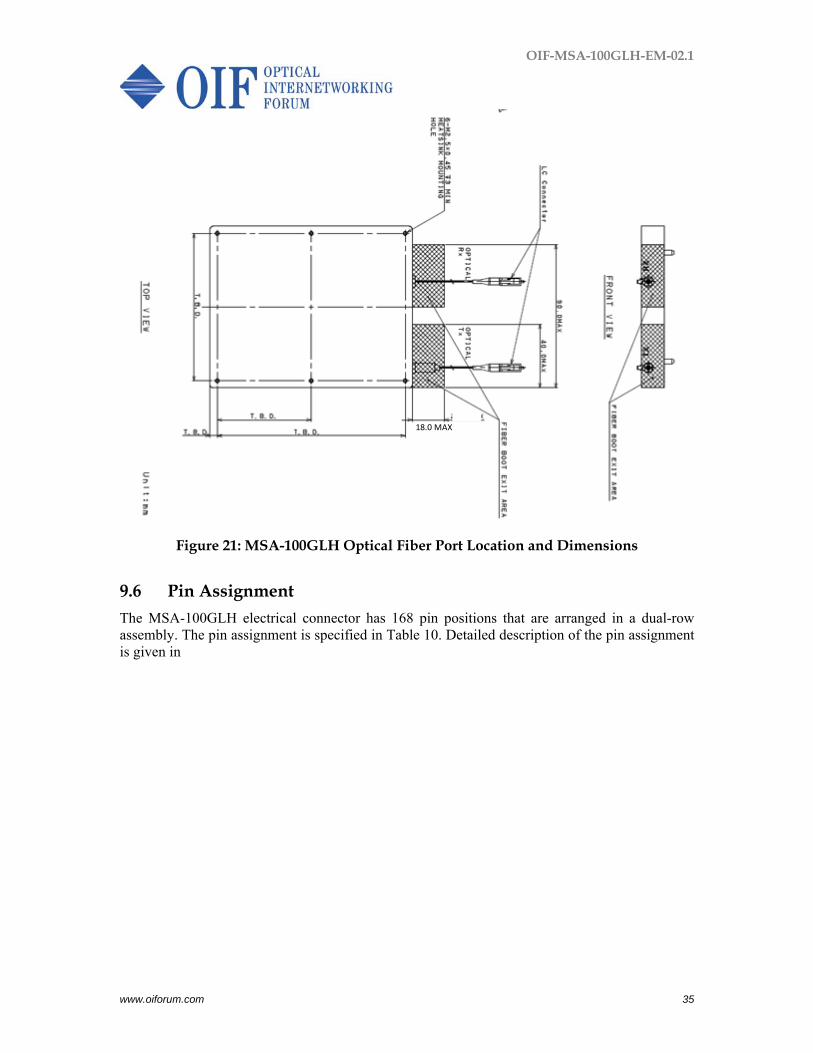
9.5 Module Optical Fiber Ports The MSA-100GLH optical transmit and receive fiber pigtail port location, dimensions and orientation are specified in Figure 21. The fiber pigtail type, length and connector type parameters are vendor specified and not specified in this document. The fiber boot exit area is solely for the purpose of indicating where the fibers are to exit the module side-wall with fiber boots for strain relief.
18.0 MAX
OIF-MSA-100GLH-EM-02.1
www.oiforum.com 35
Figure 21: MSA-100GLH Optical Fiber Port Location and Dimensions
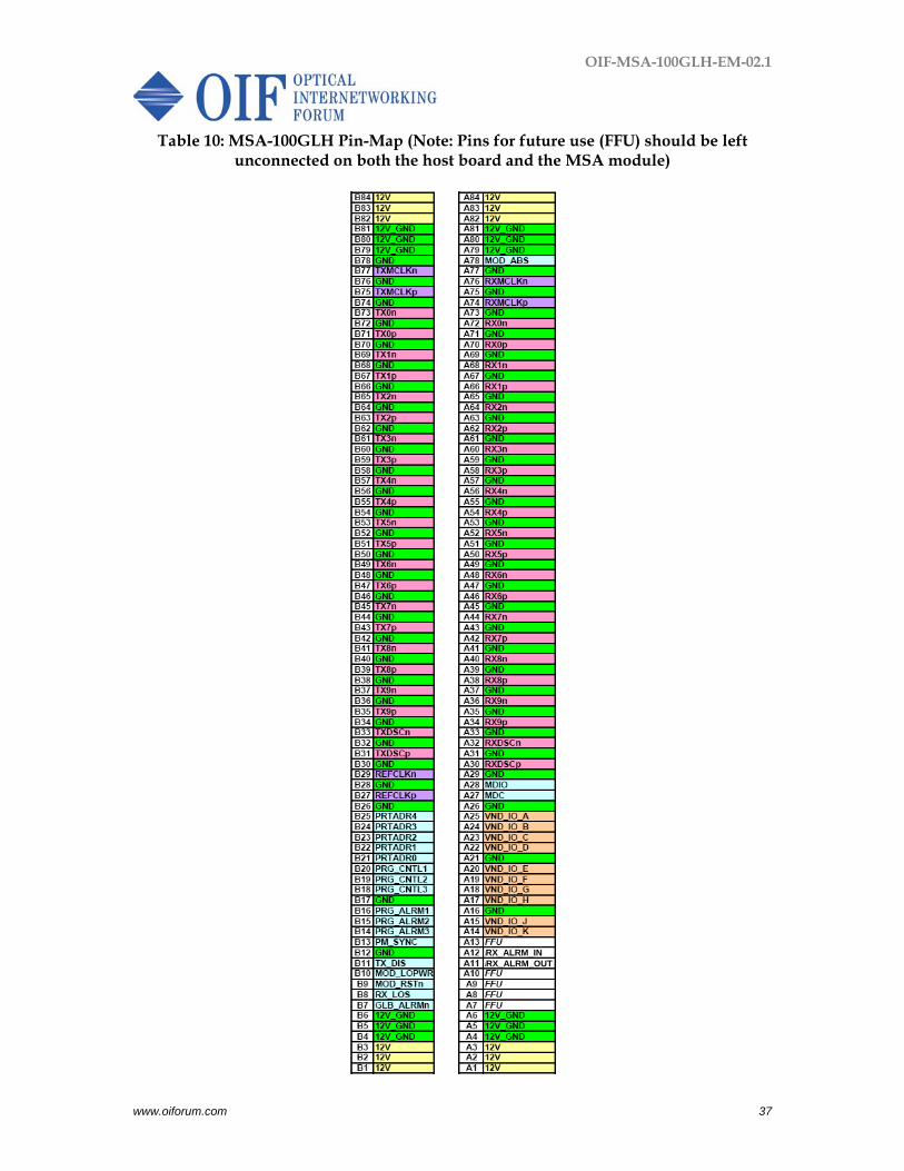
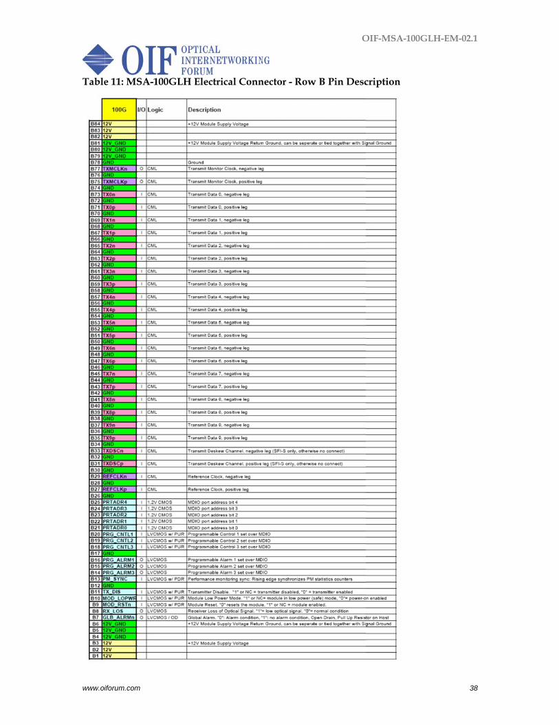
9.6 Pin Assignment The MSA-100GLH electrical connector has 168 pin positions that are arranged in a dual-row assembly. The pin assignment is specified in Table 10. Detailed description of the pin assignment is given in
18.0 MAX

OIF-MSA-100GLH-EM-02.1
www.oiforum.com 36
Table 11 and Table 12. The pin orientation is illustrated in Figure 17.
OIF-MSA-100GLH-EM-02.1
www.oiforum.com 37
Table 10: MSA-100GLH Pin-Map (Note: Pins for future use (FFU) should be left unconnected on both the host board and the MSA module)
RX_ALRM_OUTRX_ALRM_IN
www.oi
Table
iforum.com
e 11: MSA-1100GLH Elecctrical Conn
nector - Row
O
w B Pin Desc
OIF-MSA-100
cription
0GLH-EM-02
3
2.1
38
OIF-MSA-100GLH-EM-02.1
www.oiforum.com 39
Table 12: MSA-100GLH Electrical Connector - Row A Pin Description (Note: Pins for future use (FFU) should be left unconnected on both the host board and the module)
O LVCMOSI LVCMOS ‐
RX_ALRM_OUTRX_ALRM_IN Receiver Alarm transfer input for Re-generator mode
Receiver Alarm transfer output for Re-generator mode
OIF-MSA-100GLH-EM-02.1
www.oiforum.com 40
10 References 10.1 Normative references [N1] IEEE 802.3ba™ -2010 “Amendment: Media Access Control Parameters, Physical Layers and Management Parameters for 40Gb/s and 100Gb/s Operation”, Clause 45 – MDIO (March, 2010) [N2] OIF-CEI-02.0 - Common Electrical I/O (CEI) - Electrical and Jitter Interoperability agreements for 6G+ bps and 11G+ bps I/O (February 2005) [N3] Hirose FX10 Datasheets: http://www.hiroseusa.com/Special_downloads18.asp 10.2 Informative references [I1] OIF-FD-100G-DWDM-01.0 - 100G Ultra Long Haul DWDM Framework Document (June 2009) [I2] ITU-T Rec. G.709/Y.1331 (v4.2 – Feb. 2012) Interfaces for the Optical Transport Network (OTN) [I3] OIF-SFI-S-01.0 – Scalable Serdes Framer Interface (SFI-S): Implementation for Interfaces Beyond 40G for Physical Layer Devices (Nov. 2008) [I4] Hirose FX10 PCB Routing Guideline: http://www.hiroseusa.com/FX10_PCB_routing_guideline_v1.2.pdf [I5] CFP MSA Management Interface Specification V2.2, r06a (July 1, 2013) 11 Appendix A: Glossary ADC Analog Digital Converter CDR Clock and Data Recovery CN Connector CML Current Mode Logic CMOS Complementary Metal Oxide Semiconductor DEC Decoder DSP Digital Signal Processor DWDM Dense Wavelength Division Multiplex ENC Encoder FEC Forward Error Correction FFU For Future Use Gbaud 109 Symbols Per Second GH Guide pin Hole GND Ground GP Guide Pin IA Implementation Agreement LVCMOS Low Voltage CMOS MDC Management Data Clock MDIO Management Data Input/Output NC No Connect OIF Optical Internetworking Forum OTL Optical channel Transport Lane PCB Printed Circuit Board PM-QPSK Polarization Multiplexed Quaternary Phase Shift Keying RX Receiver
OIF-MSA-100GLH-EM-02.1
www.oiforum.com 41
SFI Serdes Framer Interface TX Transmitter VND Vendor 12 Appendix B: Open Issues / current work items None.

OIF-MSA-100GLH-EM-02.1
www.oiforum.com 42
13 Appendix C: List of companies belonging to OIF when
document is approved Acacia Communications Kaiam ADVA Optical Networking Kandou Alcatel-Lucent KDDI R&D Laboratories Altera Keysight Technologies, Inc. AMCC LeCroy Amphenol Corp. Luxtera Analog Devices M/A-COM Technology Solutions Anritsu Mellanox Technologies Applied Communication Sciences Microsemi Inc. Avago Technologies Inc. Microsoft Corporation Broadcom Mitsubishi Electric Corporation Brocade Molex BRPhotonics MoSys, Inc. BTI Systems MultiPhy Ltd China Telecom NEC Ciena Corporation NeoPhotonics Cisco Systems NTT Corporation ClariPhy Communications Oclaro Coriant R&G GmbH Orange CPqD PacketPhotonics Deutsche Telekom PETRA Dove Networking Solutions Picometrix EMC Corp PMC Sierra Emcore QLogic Corporation Ericsson Qorvo ETRI Ranovus FCI USA LLC Rockley Photonics Fiberhome Technologies Group Samtec Inc. Finisar Corporation Semtech Fujikura Spirent Communications Fujitsu Sumitomo Electric Industries Furukawa Electric Japan Sumitomo Osaka Cement Google TE Connectivity Hewlett Packard Tektronix Hitachi TELUS Communications, Inc. Huawei Technologies TeraXion IBM Corporation Texas Instruments
OIF-MSA-100GLH-EM-02.1
www.oiforum.com 43
Infinera Time Warner Cable Inphi US Conec Intel Verizon Ixia Xilinx JDSU Yamaichi Electronics Ltd. Juniper Networks ZTE Corporation
- End of Document -