ic design introduction - · pdf file(verilog, vhdl, etc.) - + + vendor ... ic design...
TRANSCRIPT

Copyright © 2011 Synopsys, Inc.
Low Power Design Methods:
Design Flows and Kits
Shushanik Karapetyan
1st year PhD Student
Synopsys Armenia Educational Department,
State Engineering University of Armenia
Moscow
March 23, 2011
Copyright © 2011 Synopsys, Inc.
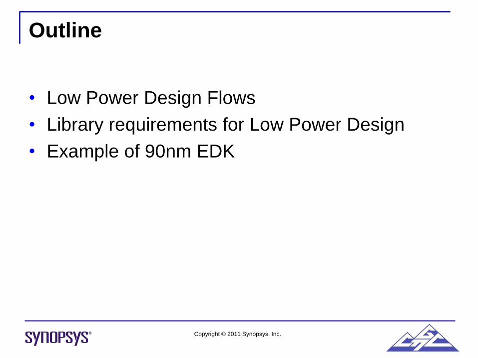
Outline
• Low Power Design Flows
• Library requirements for Low Power Design
• Example of 90nm EDK
Copyright © 2011 Synopsys, Inc.
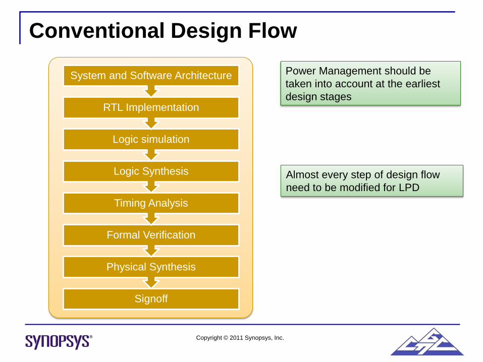
Conventional Design Flow
Signoff
Physical Synthesis
Formal Verification
Timing Analysis
Logic Synthesis
Logic simulation
RTL Implementation
System and Software Architecture
Almost every step of design flow
need to be modified for LPD
Power Management should be
taken into account at the earliest
design stages
Copyright © 2011 Synopsys, Inc.
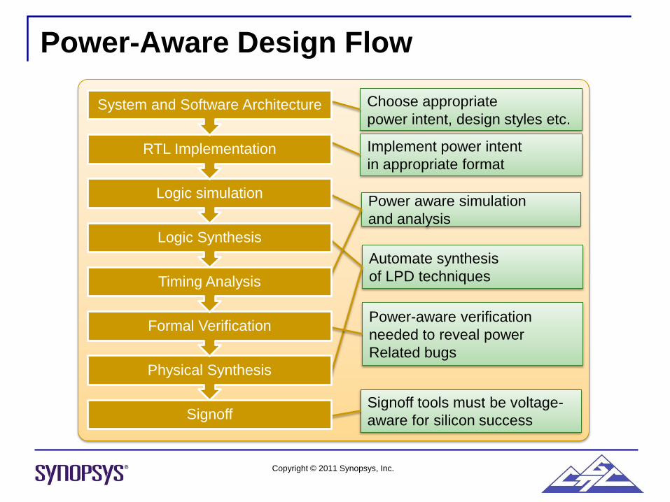
Power-Aware Design Flow
Signoff tools must be voltage-
aware for silicon success
Choose appropriate
power intent, design styles etc.
Power-aware verification
needed to reveal power
Related bugs
Automate synthesis
of LPD techniques
Implement power intent
in appropriate format
Power aware simulation
and analysis
Signoff
Physical Synthesis
Formal Verification
Timing Analysis
Logic Synthesis
Logic simulation
RTL Implementation
System and Software Architecture
Copyright © 2011 Synopsys, Inc.
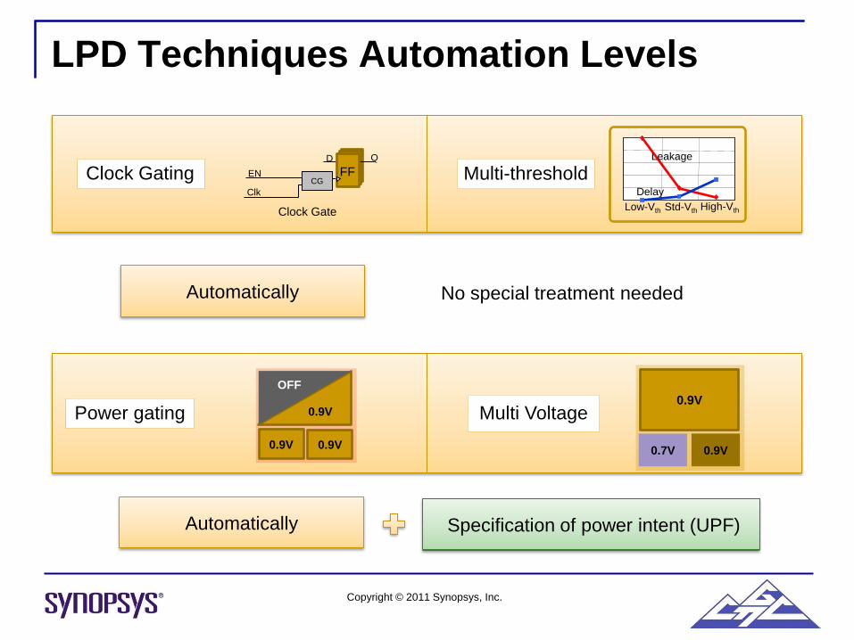
LPD Techniques Automation Levels
Power gating Multi Voltage
Low-Vth Std-Vth High-Vth
Leakage
DelayClk
Clock Gate
EN
D Q
FFCG
0.9V0.7V
0.9V
Clock Gating Multi-threshold
0.9V
0.9V
OFF
0.9V
Automatically
Automatically Specification of power intent (UPF)
No special treatment needed

Copyright © 2011 Synopsys, Inc.
Unified Power Format (UPF): Necessity
LanguageSpecification of
power intent
Interoperable
among EDA tools
Can be freely used
(open standard)
Hardware
Description
Languages
(Verilog, VHDL, etc.)
- + +
Vendor –Specific
Formats + - -
UPF + + +

Copyright © 2011 Synopsys, Inc.
Specifying Power Intent
0.9V0.7V/1.2V
MV with power gating
Power Domain
Operation Scenario
(OFF, 0.9V, 0.7V)
(0.9V, 0.9V, 1.2V)
LS
LS
LS
LS
OFF
0.9V
0.9/OFF
•iso
A
B C
Supply Network
Periphery

Copyright © 2011 Synopsys, Inc.
MV with Power Gating Example
0.9V
LS
LS
LS
LS
OFF
0.9V
0.9/OFF
•iso
A
0.7V/1.2V
BC
VSSVSS
VSS
VSS
VDD
VDD
VDD
VDDA
VDDB
VDDA
VDDB
RRVDDV
Control

Copyright © 2011 Synopsys, Inc.
UPF: Power Domains
0.9V
LS
LS
LS
LS
OFF
0.9V
0.9/OFF
•iso
A
0.7V/1.2V
BC
VSSVSS
VSS
VSS
VDD
VDD
VDD
VDDA
VDDB
VDDA
VDDB
RR
LS
VDDV
Control
Power
Domain
Power
State
A 0.9/OFF
B 0.7/1.2
C 0.9
UPF

Copyright © 2011 Synopsys, Inc.
UPF: Supply Network
0.9V
LS
LS
LS
LS
OFF
0.9V
0.9/OFF
•iso
A
0.7V/1.2V
BC
VSSVSS
VSS
VSS
VDD
VDD
VDD
VDDA
VDDB
VDDA
VDDB
RR
LS
VDDV
Control
Supply
Net
Voltage
Level (V)
Power
Domain
VDD 0.9 C
VDDA 0.7 B
VDDB 1.2 B
VDDV Virtual 0.9 A
VSS Common
Ground
A/B/C
UPF

Copyright © 2011 Synopsys, Inc.
UPF: Periphery
0.9V
LS
LS
LS
LS
OFF
0.9V
0.9/OFF
•iso
A
0.7V/1.2V
BC
VSSVSS
VSS
VSS
VDD
VDD
VDD
VDDA
VDDB
VDDA
VDDB
RR
LS
VDDV
Control
Required Periphery
Level Shifters between A and B
Level Shifters between B and C
Isolation between C and A
Retention Cell inside A
Control Block inside A
UPF
Copyright © 2011 Synopsys, Inc.
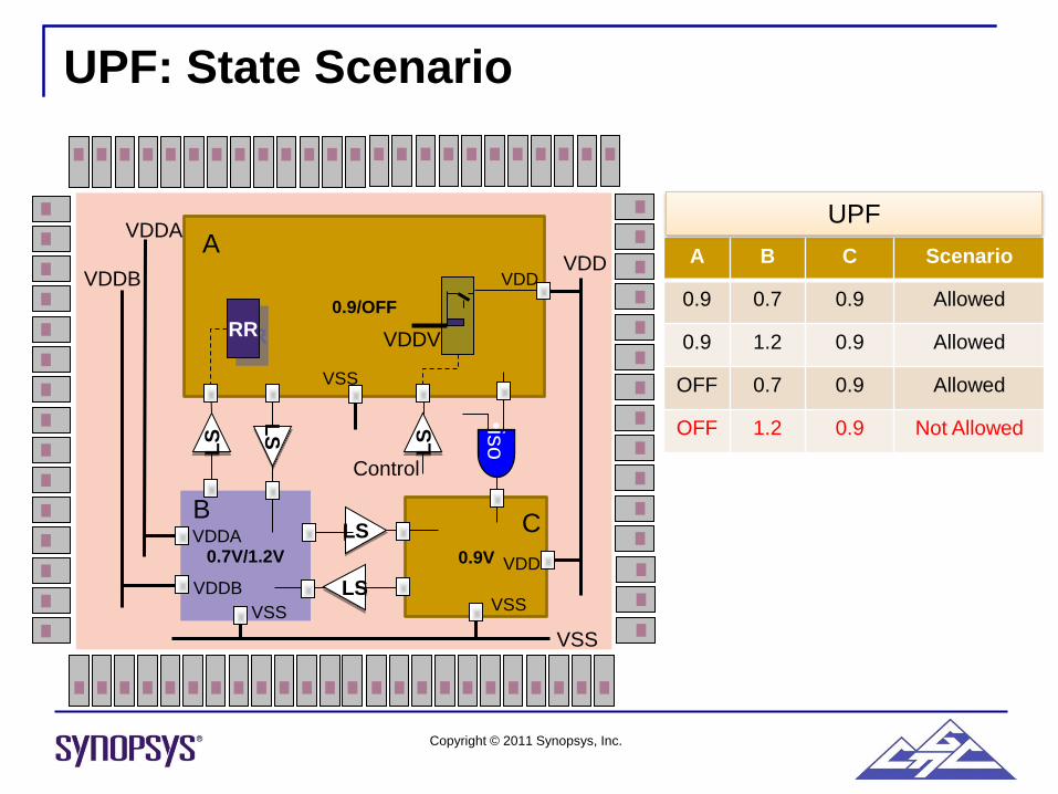
UPF: State Scenario
0.9V
LS
LS
LS
LS
OFF
0.9V
0.9/OFF
•iso
A
0.7V/1.2V
BC
VSSVSS
VSS
VSS
VDD
VDD
VDD
VDDA
VDDB
VDDA
VDDB
RR
LS
VDDV
Control
A B C Scenario
0.9 0.7 0.9 Allowed
0.9 1.2 0.9 Allowed
OFF 0.7 0.9 Allowed
OFF 1.2 0.9 Not Allowed
UPF
Copyright © 2011 Synopsys, Inc.
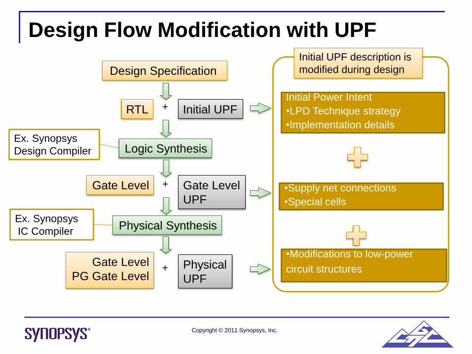
Design Flow Modification with UPF
Design Specification
RTL Initial UPF
Logic Synthesis
Gate Level Gate Level
UPF
Physical Synthesis
Gate Level
PG Gate LevelPhysical
UPF
+
+
+
•Supply net connections
•Special cells
•Modifications to low-power
circuit structures
Initial Power Intent
•LPD Technique strategy
•Implementation details
Initial UPF description is
modified during design
Ex. Synopsys
Design Compiler
Ex. Synopsys
IC Compiler
Copyright © 2011 Synopsys, Inc.
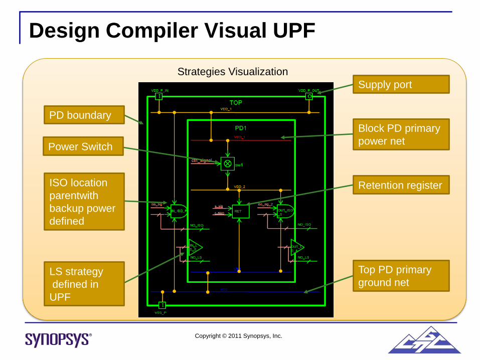
Design Compiler Visual UPF
Strategies Visualization
Supply port
Block PD primary
power net
Retention register
Top PD primary
ground net LS strategy
defined in
UPF
ISO location
parentwith
backup power
defined
Power Switch
PD boundary
Copyright © 2011 Synopsys, Inc.
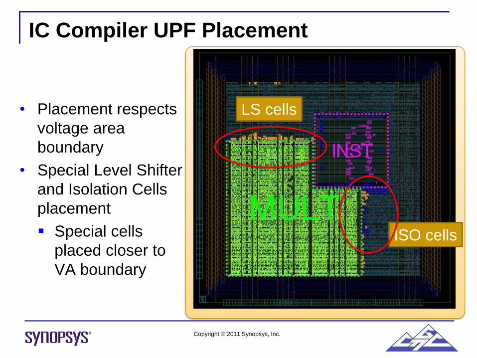
IC Compiler UPF Placement
• Placement respects
voltage area
boundary
• Special Level Shifter
and Isolation Cells
placement
Special cells
placed closer to
VA boundary
ISO cells
LS cells
Copyright © 2011 Synopsys, Inc.
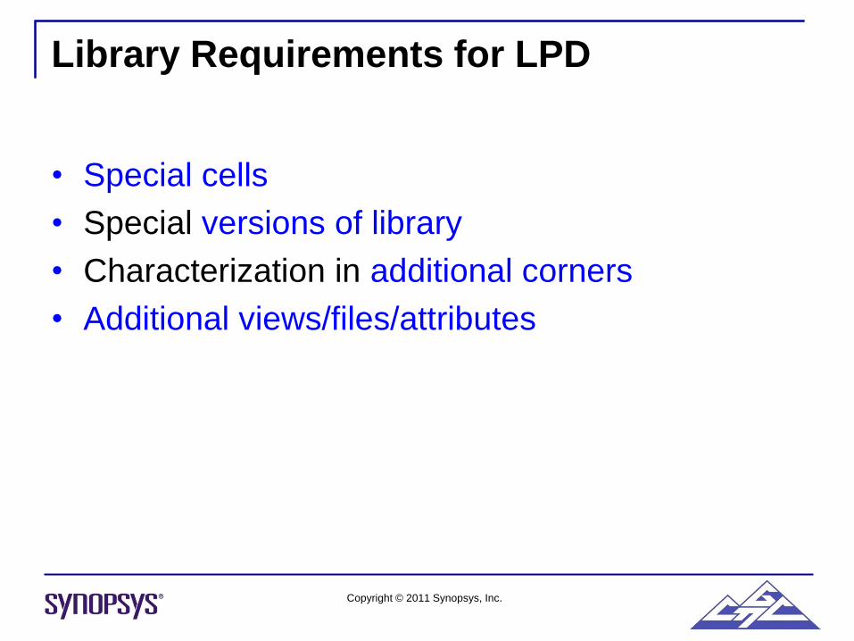
Library Requirements for LPD
• Special cells
• Special versions of library
• Characterization in additional corners
• Additional views/files/attributes

Copyright © 2011 Synopsys, Inc.
Aimed at optimizing the main characteristics of designed Ics
Contains 340 cells, cell list compiled based on the requirements for educational designs
Typical combinational and sequential logic cells for different drive strengths
Provides the support of IC design with different core voltages to minimize dynamic and leakage power.
Typical combinational and sequential Special cells for different styles LPD
90nm EDK: Digital Standard Cell Library
Isolation Cells Level ShiftersRetention Flip-Flops
Clock gatingAlways-on
BuffersPower Gating
Digital Standard Cell Library (DSCL)
Inverters/Buffers Logic GatesFlip-Flops
(regular+scan)
Latches Delay LinesPhysical
(Antenna diode)
Copyright © 2011 Synopsys, Inc.
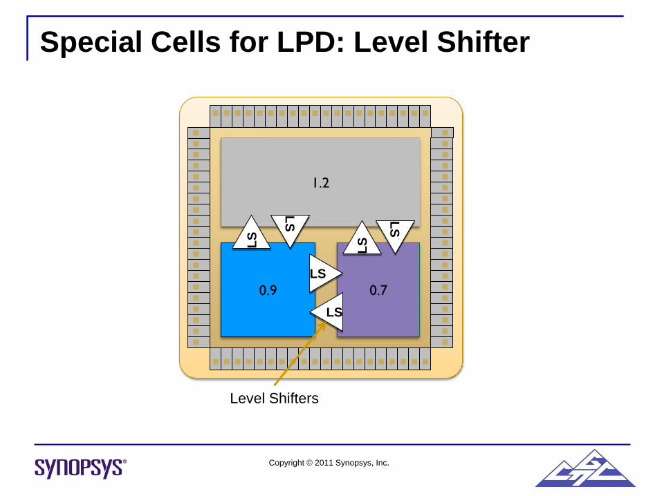
Special Cells for LPD: Level Shifter
0.9 0.7
1.2
LS
LS
LS
LS
LS
LS
Level Shifters
Copyright © 2011 Synopsys, Inc.
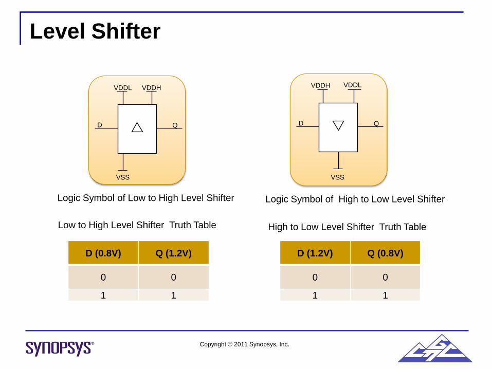
Level Shifter
Logic Symbol of Low to High Level Shifter
Low to High Level Shifter Truth Table
QD
VSS
VDDL VDDH
QD
VSS
VDDH VDDL
Logic Symbol of High to Low Level Shifter
High to Low Level Shifter Truth Table
D (0.8V) Q (1.2V)
0 0
1 1
D (1.2V) Q (0.8V)
0 0
1 1
Copyright © 2011 Synopsys, Inc.
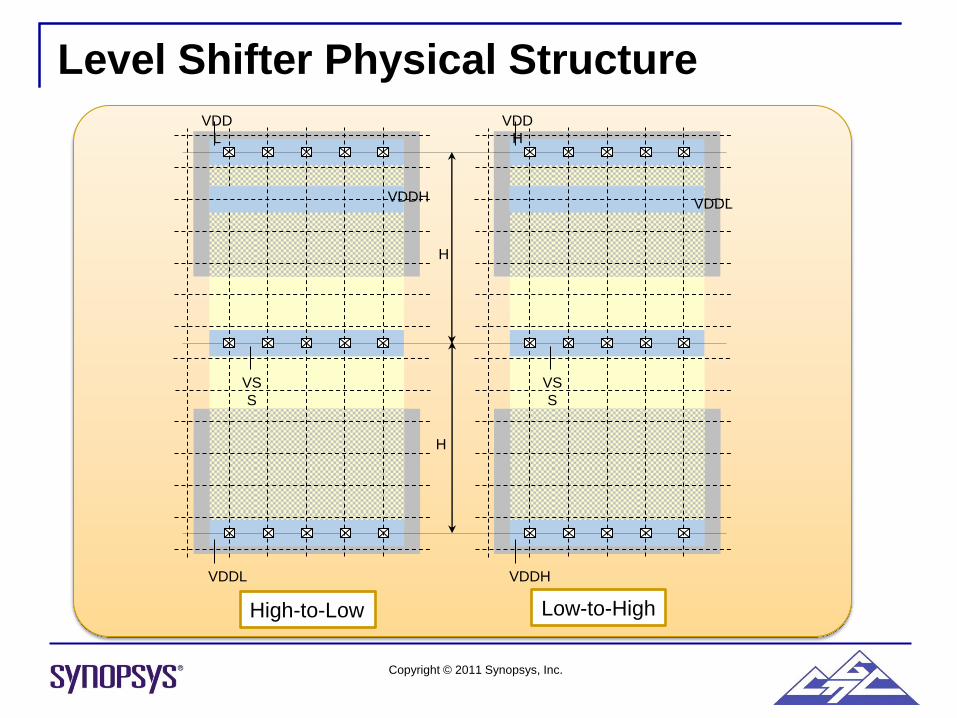
Level Shifter Physical Structure
VDDL
VDD
L
H
H
VS
S
VDDH
VDDH
VDD
H
VS
S
VDDL
High-to-Low Low-to-High
Copyright © 2011 Synopsys, Inc.
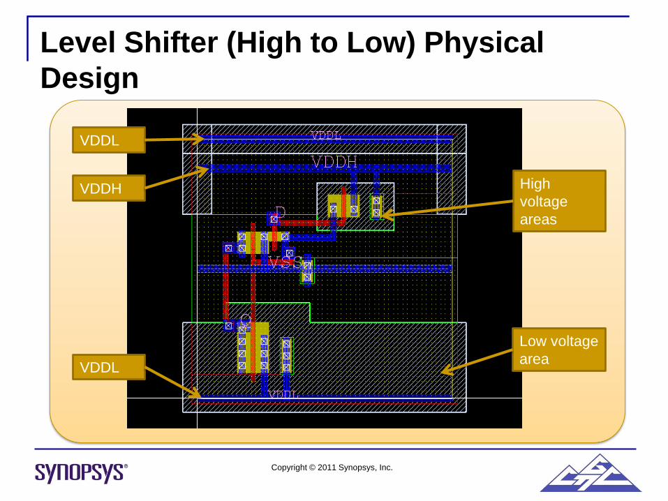
Level Shifter (High to Low) Physical
Design
Low voltage
area
High
voltage
areas
VDDH
VDDL
VDDL
Copyright © 2011 Synopsys, Inc.
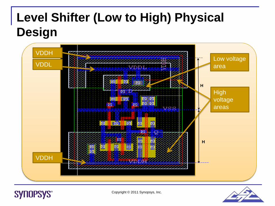
Level Shifter (Low to High) Physical
Design
Low voltage
area
High
voltage
areas
H
H
VDDH
VDDH
VDDL

Copyright © 2011 Synopsys, Inc.
Special Cells for LPD: Isolation Cells
0.9
0.9
Isolation Cells
Power Gating
OFF/0.7
Copyright © 2011 Synopsys, Inc.
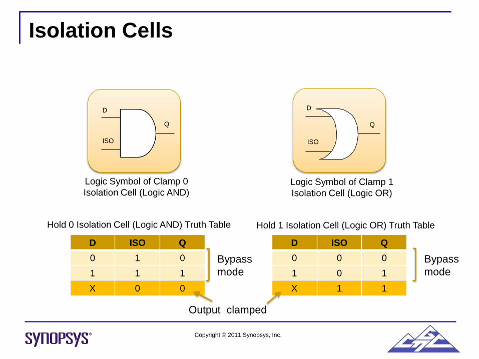
Isolation Cells
D
Q
ISO
Logic Symbol of Clamp 0
Isolation Cell (Logic AND)
Hold 0 Isolation Cell (Logic AND) Truth Table Hold 1 Isolation Cell (Logic OR) Truth Table
Logic Symbol of Clamp 1
Isolation Cell (Logic OR)
D ISO Q
0 1 0
1 1 1
X 0 0
D ISO Q
0 0 0
1 0 1
X 1 1
D
Q
ISO
Output clamped
Bypass
mode
Bypass
mode
Copyright © 2011 Synopsys, Inc.
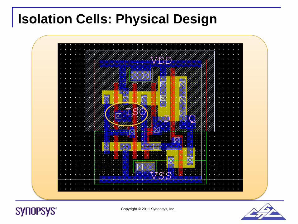
Isolation Cells: Physical Design

Copyright © 2011 Synopsys, Inc.
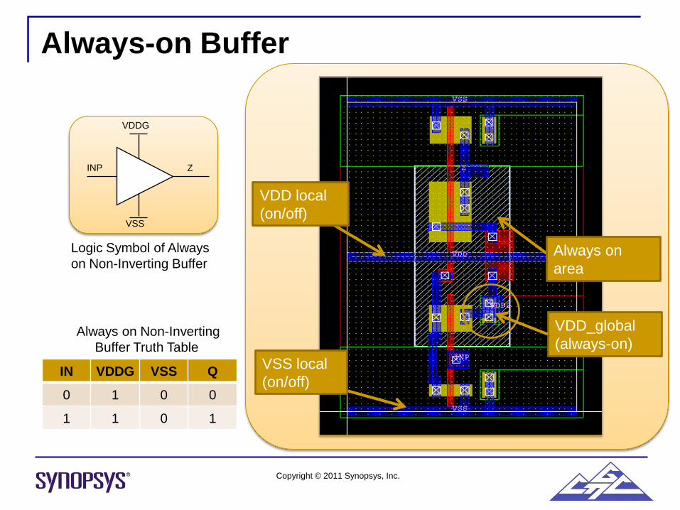
Special Cells for LPD: Always-on Buffers
0.9
0.7 – 1.08
Always on cells
Power Gating
OFF/0.7
Copyright © 2011 Synopsys, Inc.
Always-on Buffer
VDD_global
(always-on)
VDD local
(on/off)
VSS local
(on/off)
Always on
area
INP Z
VDDG
VSS
Logic Symbol of Always
on Non-Inverting Buffer
Always on Non-Inverting
Buffer Truth Table
IN VDDG VSS Q
0 1 0 0
1 1 0 1
Copyright © 2011 Synopsys, Inc.
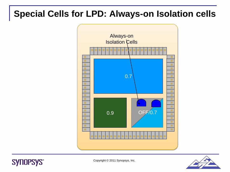
Special Cells for LPD: Always-on Isolation cells
0.9
0.7
Always-on
Isolation Cells
OFF/0.7

Copyright © 2011 Synopsys, Inc.
Always on Isolation Cells
Logic Symbol of Clamp 0 Isolation Cell
(Logic AND),Always On
D
Q
ISO
VSS
VDD VDDG
Logic Symbol of Clamp 1 Isolation Cell
(Logic OR), Always On
VDD
VSS
VDDG
D
Q
ISO
Hold 0 Isolation Cell (Logic AND) Truth Table Hold 1 Isolation Cell (Logic OR) Truth Table
D ISO Q
0 1 0
1 1 1
X 0 0
D ISO Q
0 0 0
1 0 1
X 1 1
Output clamped
Bypass
mode
Bypass
mode
Copyright © 2011 Synopsys, Inc.
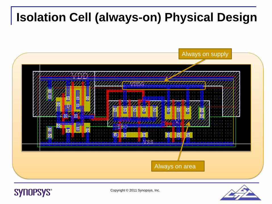
Isolation Cell (always-on) Physical Design
Always on area
Always on supply

Copyright © 2011 Synopsys, Inc.
Special Cells for LPD: Enable level
shifters
• Combination of Level
Shifter and ISO cell
0.9
1.08
Enable level
shifters
OFF/0.7
Copyright © 2011 Synopsys, Inc.
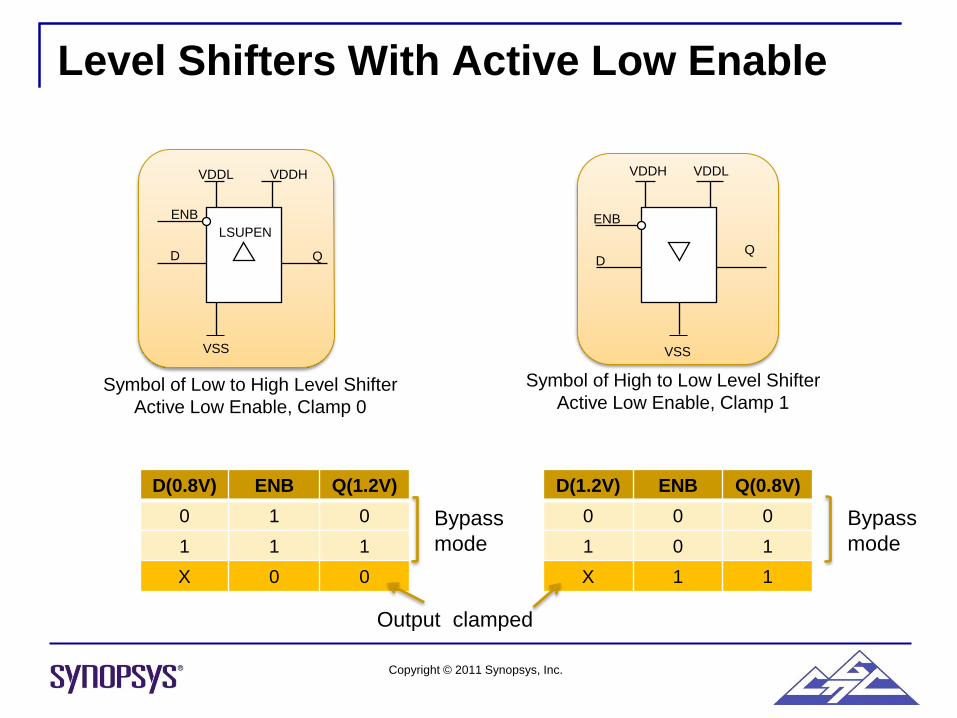
Level Shifters With Active Low Enable
QD
VSS
VDDL VDDH
LSUPEN
ENB
Q
ENB
D
VSS
VDDLVDDH
Symbol of High to Low Level Shifter
Active Low Enable, Clamp 1Symbol of Low to High Level Shifter
Active Low Enable, Clamp 0
D(0.8V) ENB Q(1.2V)
0 1 0
1 1 1
X 0 0
D(1.2V) ENB Q(0.8V)
0 0 0
1 0 1
X 1 1
Output clamped
Bypass
mode
Bypass
mode
Copyright © 2011 Synopsys, Inc.
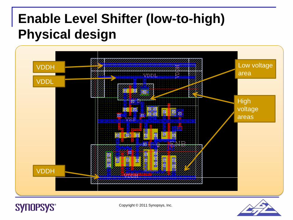
Enable Level Shifter (low-to-high)
Physical design
Low voltage
area
High
voltage
areas
VDDH
VDDH
VDDL
Copyright © 2011 Synopsys, Inc.
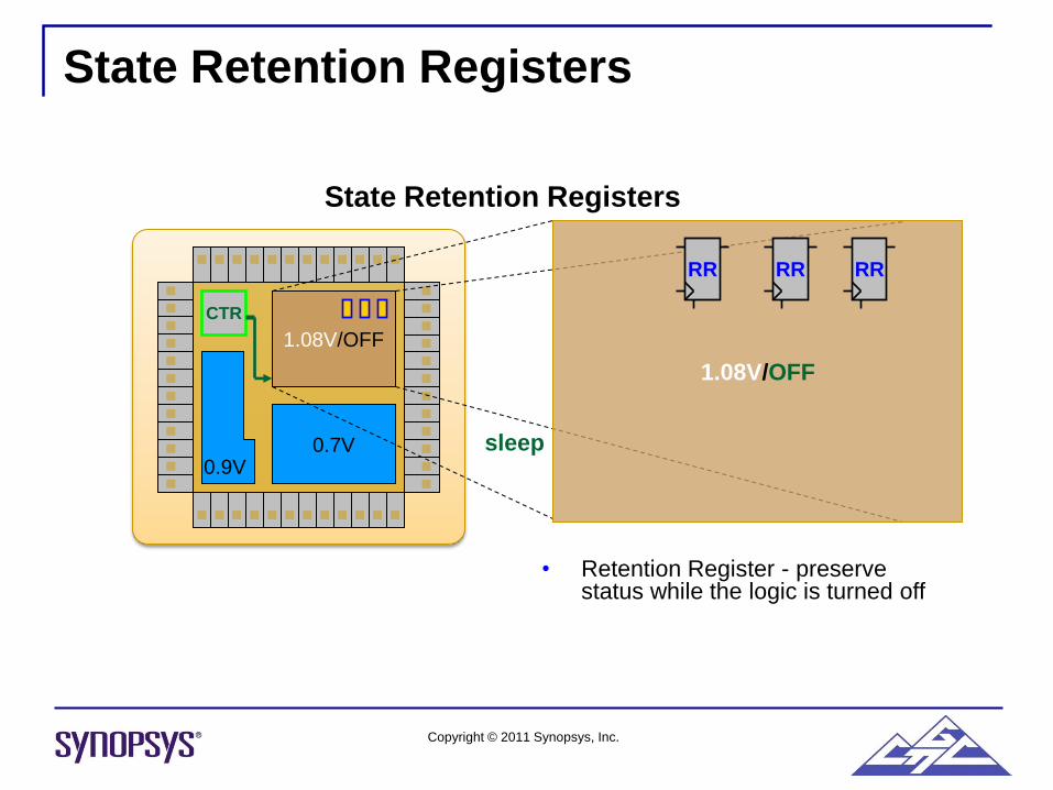
State Retention Registers
State Retention Registers
• Retention Register - preserve status while the logic is turned off
1.08V/OFF
0.7V0.9V
CTR
1.08V/OFF
sleep
RRRRRR
Copyright © 2011 Synopsys, Inc.
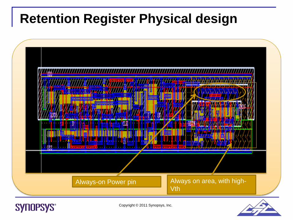
Always on area, with high-
Vth
Retention Register Physical design
Always-on Power pin
Copyright © 2011 Synopsys, Inc.
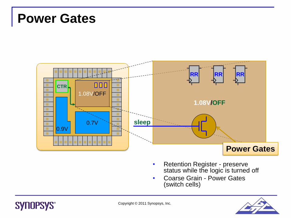
Power Gates
• Retention Register - preserve status while the logic is turned off
• Coarse Grain - Power Gates (switch cells)
1.08V/OFF
0.7V0.9V
CTR
1.08V/OFF
sleep
RRRRRR
Power Gates
Copyright © 2011 Synopsys, Inc.
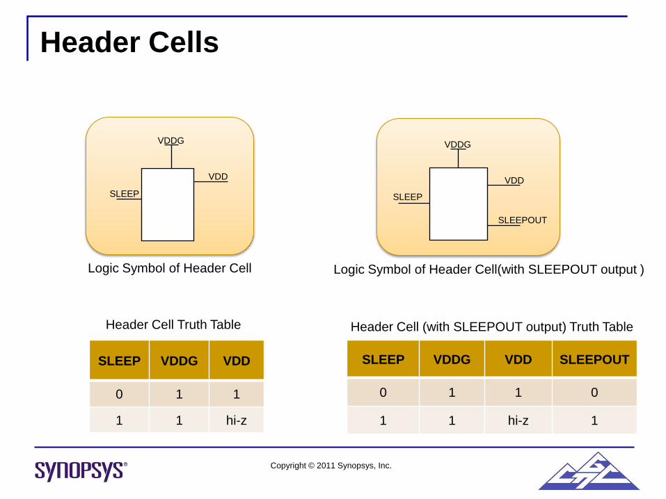
Header Cells
VDD
SLEEP
VDDG
VDD
SLEEPOUT
SLEEP
VDDG
Logic Symbol of Header Cell(with SLEEPOUT output )
Header Cell (with SLEEPOUT output) Truth Table
Logic Symbol of Header Cell
Header Cell Truth Table
SLEEP VDDG VDD
0 1 1
1 1 hi-z
SLEEP VDDG VDD SLEEPOUT
0 1 1 0
1 1 hi-z 1
Copyright © 2011 Synopsys, Inc.
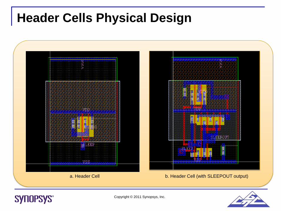
Header Cells Physical Design
a. Header Cell b. Header Cell (with SLEEPOUT output)

Copyright © 2011 Synopsys, Inc.
Multi-Threshold Libraries
AL BL CL
AS BS CS
AH BH CH
Low Vth
Std Vth
High Vth
Multi-Vth libraries
Low-Vth Std-Vth High-Vth
0%
20%
40%
60%
80%
100%
Leakage Delay
FFFF
FF
FFFF
Critical
Path

Copyright © 2011 Synopsys, Inc.
DSCL: Multi Threshold Versions of Cells
• For implementation of Multi-Vth technique the
whole DSCL is available in 3 versions (1020
cells)
All cells with Low– threshold voltage
All cells with Standard – threshold voltage
All cells with High– threshold voltage

Copyright © 2011 Synopsys, Inc.
Characterization
• Characterization computes cell parameter (e.g. delay, output
current) depending on input variables: output load, input slew, etc.
• Characterization is preformed for various combinations of operating
conditions: process, voltage, temperature (also called PVT corners).
0.7
0.5
0.2
0.1
.023 .047 .065 .078 .091output cap
slew
0.7
0.5
0.2
0.1
.023 .047 .065 .078 .091output cap
slew
Iout
Cchar
Input Slew
0.7
0.5
0.2
0.1
.023 .047 .065 .078 .091output cap
slew
Process: Typical
Temp: 25o
Voltage: 1.2v
Process: Slow
Temp: -40o
Voltage: 1.08v
Process: Fast
Temp: 125o
Voltage: 1.32v
Copyright © 2011 Synopsys, Inc.
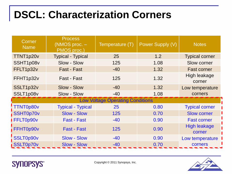
Corner
Name
Process
(NMOS proc. –
PMOS proc.)
Temperature (T) Power Supply (V) Notes
TTNT1p20v Typical - Typical 25 1.2 Typical corner
SSHT1p08v Slow - Slow 125 1.08 Slow corner
FFLT1p32v Fast - Fast -40 1.32 Fast corner
FFHT1p32v Fast - Fast 125 1.32High leakage
corner
SSLT1p32v Slow - Slow -40 1.32 Low temperature
cornersSSLT1p08v Slow - Slow -40 1.08
Low Voltage Operating Conditions
TTNT0p80v Typical - Typical 25 0.80 Typical corner
SSHT0p70v Slow - Slow 125 0.70 Slow corner
FFLT0p90v Fast - Fast -40 0.90 Fast corner
FFHT0p90v Fast - Fast 125 0.90High leakage
corner
SSLT0p90v Slow - Slow -40 0.90 Low temperature
cornersSSLT0p70v Slow - Slow -40 0.70
DSCL: Characterization Corners
Copyright © 2011 Synopsys, Inc.
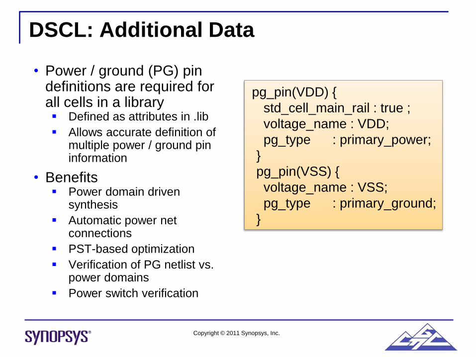
DSCL: Additional Data
• Power / ground (PG) pin definitions are required for all cells in a library Defined as attributes in .lib
Allows accurate definition of multiple power / ground pin information
• Benefits Power domain driven
synthesis
Automatic power net connections
PST-based optimization
Verification of PG netlist vs. power domains
Power switch verification
pg_pin(VDD) {
std_cell_main_rail : true ;
voltage_name : VDD;
pg_type : primary_power;
}
pg_pin(VSS) {
voltage_name : VSS;
pg_type : primary_ground;
}
Copyright © 2011 Synopsys, Inc.
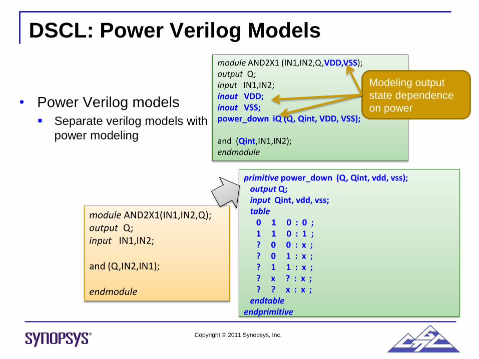
DSCL: Power Verilog Models
module AND2X1 (IN1,IN2,Q,VDD,VSS);output Q;input IN1,IN2;inout VDD;inout VSS;power_down iQ (Q, Qint, VDD, VSS);
and (Qint,IN1,IN2);endmodule
module AND2X1(IN1,IN2,Q);output Q;input IN1,IN2;
and (Q,IN2,IN1);
endmodule
primitive power_down (Q, Qint, vdd, vss);output Q;input Qint, vdd, vss;table
0 1 0 : 0 ;1 1 0 : 1 ;? 0 0 : x ;? 0 1 : x ;? 1 1 : x ;? x ? : x ;? ? x : x ;
endtableendprimitive
Modeling output
state dependence
on power• Power Verilog models
Separate verilog models with
power modeling

Copyright © 2011 Synopsys, Inc.
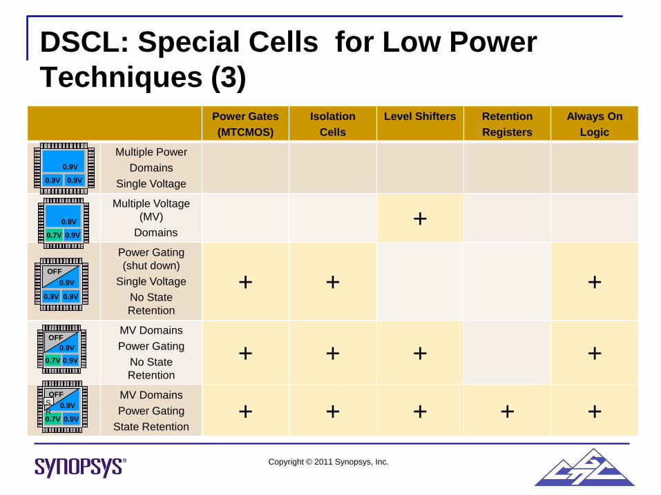
DSCL: Special Cells for Low Power
Techniques (1)
• Power Gatings
5 cells with different loads
• Always on
10 cells: 3 inverters, 3 buffers and
4 DFFs
• Retention cells
44 cells negedge/posedge, scan
• Isolation cells
8 cells with different logic, load
Q
QN
D
CLK
VSS
VDD VDDG
RETN
IN Q
VDDG
VSS
AOnVDD
SLEEP
VDDG
DQ
ISO
ISO

Copyright © 2011 Synopsys, Inc.
QD
VSS
VDDL VDDH
LSUP
GCLK
EN
CLK
SE
L
A
T
C
H
OBS
ENL
DSCL: Special Cells for Low Power
Techniques (2)
• Level shifters
16 cells Low/High, High/Low, with
or without enable, with different
loads
• Clock gatings:
11 cells with different loads, edges,
and control (post/pre)
• HVT Cells
All logical cells are designed using
HVT, LVT
Copyright © 2011 Synopsys, Inc.
Power Gates
(MTCMOS)
Isolation
Cells
Level Shifters Retention
Registers
Always On
Logic
Multiple Power
Domains
Single Voltage
Multiple Voltage
(MV)
Domains+
Power Gating
(shut down)
Single Voltage
No State
Retention
+ + +
MV Domains
Power Gating
No State
Retention
+ + + +
MV Domains
Power Gating
State Retention+ + + + +
DSCL: Special Cells for Low Power
Techniques (3)
0.9V0.9V
0.9V
0.9V0.9V
0.9V
OFF
0.9V0.7V
0.9V
0.9V0.7V
0.9V
OFF
0.9V0.7V
0.9V
OFFS
R
Copyright © 2011 Synopsys, Inc.
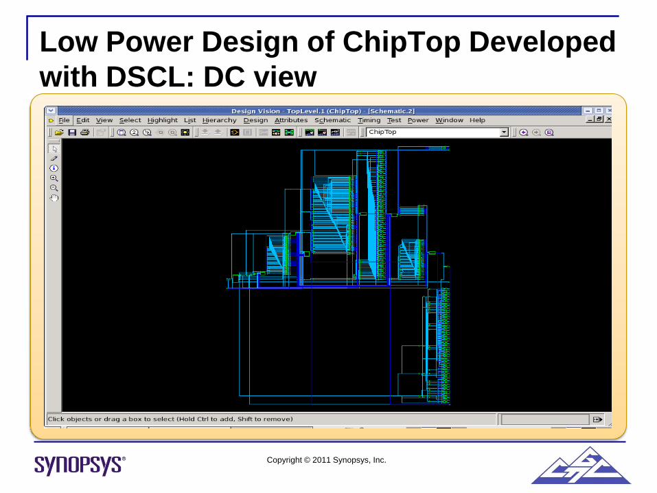
Low Power Design of ChipTop Developed
with DSCL: DC view
Copyright © 2011 Synopsys, Inc.
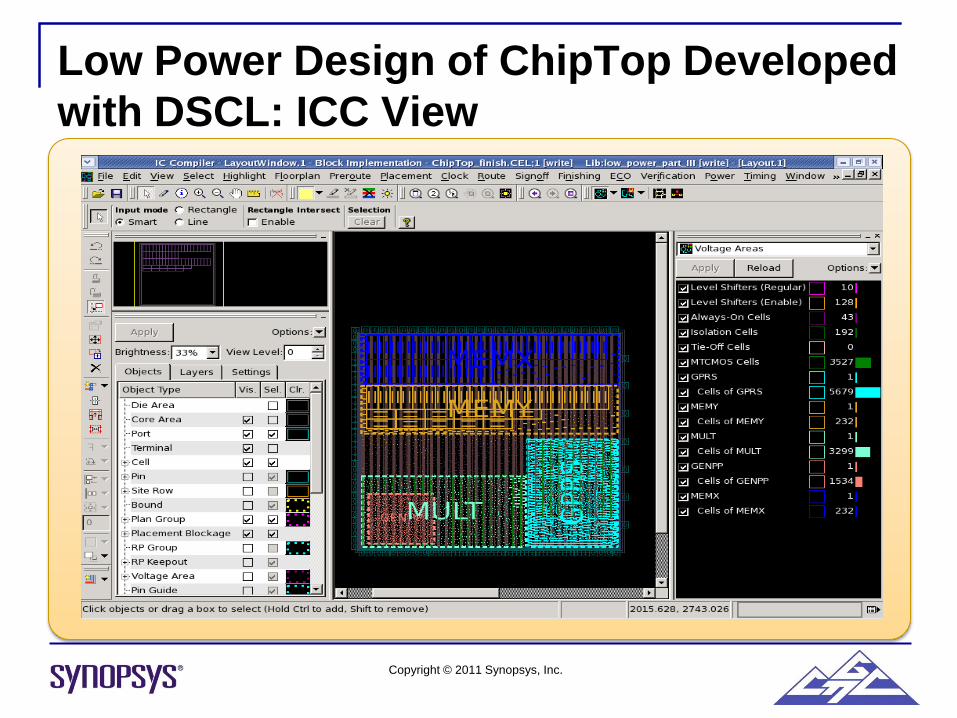
Low Power Design of ChipTop Developed
with DSCL: ICC View

Copyright © 2011 Synopsys, Inc.
Conclusion
• Low Power Design requires significant design flow modifications
UPF enables LPD flow automation
• Low Power design techniques have their huge impact on libraries
• SAED 90nm EDK DSCL includes all special cells needed for low
power design techniques
• This 90nm EDK is currently in use in 235 universities of 37 countries
• This 90nm EDK is used inside Synopsys for education of customers
• Currently similar EDK is being developed for 32/28nm technology,
initial release is planned in June 2011