ict-2009.3.2 design of semiconductor components and ... fpga platform 7 3 the system ... form of...
TRANSCRIPT

Grant Agreement number: 248972
Project acronym: NaNoC
Project title: “Nanoscale Silicon-Aware Network-on-ChipDesign Platform”
Seventh Framework Programme
Funding Scheme: STREP
Theme ICT-2009.3.2 Design of semiconductor components andelectronic based miniaturised systems
Start date of project: 01/01/2010 Duration: 36 months
D 5.3 Report on the evaluation of the network-level testing and/or(re-)configuration strategy.
Due date of deliverable: Month 36Actual submission date: Month 36
Organization name of lead beneficiary for this deliverable: UNIFEContributing partners to this deliverable: UNIFE, INOCS, UPV, SIMULAWork package contributing to the Deliverable: WP5
Dissemination LevelPU Public xPP Restricted to other programme participants (including the Commission Services)RE Restricted to a group specified by the consortium (including the Commission Services)CO Confidential, only for members of the consortium (including theCommission Services)
APPROVED BY:
Partners DateAll partners January 25th, 2013

INDEX
1 Introduction 5
2 FPGA Platform 7
3 The System Under Test 83.1 Basic components: the on-chip network . . . . . . . . . . . . . . 11
3.1.1 The Network Interfaces . . . . . . . . . . . . . . . . . . . 123.1.2 The switch . . . . . . . . . . . . . . . . . . . . . . . . . . 13
3.2 Basic components: the supervision subsystem . . . . . . . . . . . 183.3 Basic components: the reconfiguration algorithm . . . . . . . . . 193.4 The GUI infrastructure . . . . . . . . . . . . . . . . . . . . . . . 203.5 The application . . . . . . . . . . . . . . . . . . . . . . . . . . . . 223.6 The physical platform implementation . . . . . . . . . . . . . . . 24
4 Validating Built-in Self-Testing and NoC configuration 254.1 Protocol for BIST notification and configuration . . . . . . . . . 27
5 Validating Fault Detection and NoC Reconfiguration 285.1 Protocol for transient notification and reconfiguration . . . . . . 30
6 Validating NoC Virtualization 31
7 Conclusions 33
ABSTRACT
Today the converging trend toward multifunction integrated architecturesis slowed down by the lack of a proper runtime reconfiguration framework ofthe on-chip interconnect. A runtime reconfiguration is needed whenever theoccurrence of events at runtime causes the need for a different resource allo-cation, such as in the cases for graceful degradation of system performance,power management, thermal control, etc. The NaNoC project has developeddesign methods to introduce such a dynamism into the on-chip network. Thisdeliverable reports about the prototyping of such design methods on a Xil-inx Virtex-7 FPGA. Boot-time testing and configuration, runtime detection offaults, runtime reconfiguration of the routing function, dynamic virtualization ofthe interconnect fabric are especially validated on the FPGA prototype, wherea 4x4 multi-core system has been implemented and managed. The advancedform of platform control is achieved via hardware/software co-design and co-optimization.

GLOSSARY
AMBA: Advanced Microcontroller Bus ArchitectureAHB: Advanced High-Performance BusAXI: Advanced Extensible InterfaceBISD: Built-In Self-DiagnosisBIST: Built-In Self-TestBRAM: Block Random Access MemoryCMP: Chip Multi-ProcessorDC FIFO: Dual-Clock First In First OutDMR: Dual Modular RedundancyDRC/TRC: Dual/Two-Rail CheckerDUT: Device Under TestFIFO: First In First OutFSM: Finite-State MachineGALS: Globally Asynchronous Locally SynchronousGPIO: General Purpose Input OutputGPU: Graphics Processing UnitHDL: Hardware description languageID: IdentifierJTAG: Joint Test Action GroupLBDR: Logic-Based Distributed RoutingLFSR: Linear Feedback Shift RegisterMISR: Multiple Input Signature RegisterMPSoC: Multi-Processor System-on-ChipNI: Network InterfaceNoC: Network-on-ChipOSR: Overlapped Static ReconfigurationPHY: Physical LayerSEU: Single Event UpsetSoC: System-on-ChipTMR: Triple Modular RedundancyTPG: Test Pattern GeneratorUSB: Universal serial busXPS: Xilinx Platform Studio

1 Introduction
NoC design principles have recently reached a stage where they start to stabilize,in correspondence to their industrial uptake. In fact, NoCs are an indisputablereality since they implement the communication backbone of virtually all large-scale system-on-chip (SoC) designs in 45nm and below.
On the other hand, the requirements on embedded system design are farfrom stabilizing and an unmistakable trend toward enhanced reconfigurabilityis clearly underway. Reconfigurability of the HW/SW architecture would in factenable several key advantages, including on-demand functionality, on-demandacceleration, shorter time-to-market, extended product life cycles and low de-sign and maintenance costs. Supporting different degrees of reconfigurability inthe parallel hardware platform cannot be however achieved with the incremen-tal evolution of current design techniques, but requires a disruptive and holisticapproach, and a major increase in complexity. At the same time, fault tolerancewas previously an issue only for specific applications such as aerospatial. Today,due to the increased variability of components and breadth of operating environ-ments, reliability becomes relevant to mainstream applications. Similarly, newreliability challenges cannot be solved by using traditional fault tolerance tech-niques alone: the reliability approach must be part of the overall reconfigurationmethodology.
In the highly parallel landscape of modern embedded computing platforms,the system interconnect serves as the framework for platform integration and istherefore key to materializing the needed flexibility and reliability properties ofthe system as a whole. Therefore, time has come for a major revision of currentNoC architectures in the direction of increased reconfigurability and reliability.
In addition, a key property that novel NoCs cannot miss is to guarantee apotentially fast path to industry, since NoC deployment is today a reality. Animportant requirement for this purpose is the efficient testability of candidateNoC architectures. This property is very challenging due to the distributednature of NoCs and to the difficult controllability and observability of its internalcomponents. When we also consider the pin count limitations of current chips,we derive that NoCs will be most probably tested in the future via builtinself-testing (BIST) strategies.
Finally, there is an increasing need in embedded systems for implementingmultiple functionalities upon a single shared computing platform. The mainmotivation for this are the constraints set for systems size, power consumptionand/or weight. This forces tasks of different criticality to share resources andinterfere with each other. Integration of multiple software functions on a singlemulti- and many-core processor (multifunction integration) is the most efficientway of utilizing the available computing power. For a mixed-criticality multi-function integration, the NoC should be augmented to support partitioning andisolation, so that software functions can be protected from unintended inter-ferences coming from other software functions executing on the same hardwareplatform. This feature is a key enabler for the virtualization of embedded sys-tems, that is, an effective and clean way of isolating applications from hardware.
This deliverable reports on the first-time prototyping of a Network-on-Chipcapable of supporting all of the advanced features described above, and rep-resents a prove of the success of the NaNoC project. The presented prototypebuilds on the GPNaNoC switch presented in deliverable D5.1 and raises the level

of abstraction to the network as a whole. Then, it validates the (re-) configura-tion capabilities that preserve safe network operation in the presence of wanted(e.g., virtualization) and unwanted (e.g., manufacturing defects, intermittentfaults) effects. The prototyping platform is represented by the Xilinx Virtex-7evaluation board named VC707, described in Section 2. The prototyped systemimplemented inside the FPGA is a homogeneous multicore processor, whichresembles programmable hardware accelerators of hierarchical, high-end em-bedded systems, or basic computation clusters of many-core processors. Thevalidated design methods include:
• boot-time testing and diagnosis of the 4x4 2D mesh NoC, targeting per-manent faults;
• switch-level and network-level fault-tolerance, targeting transient faultsand intermittent faults (i.e., those faults that rapidly anticipate the break-down of links or switch components;
• runtime reconfiguration of the network routing function, with logic-baseddistributed routing as the underlying routing mechanism. The validatedreconfiguration procedures are twofold: at boot-time, without backgroundtraffic, and at runtime, with background traffic.
• Dynamic virtualization, i.e., partitioning of the whole NoC into isolatedpartitions running different applications.
As such, this deliverable validates:
• the design methods for supporting NoC static irregularities developed inWP1 (routing methods, testing and diagnosis methods);
• the design methods for supporting dynamically virtualized NoCs devel-oped in WP2 (error detection and signaling mechanisms, runtime recon-figuration methods, virtualization methodology);
• methodologies for seamless integration of NoC topologies within IP cores,from WP3.
The remaining technical WPs (the bulk of WP3, and WP4) will be validatedin deliverable D5.2.
Looking beyond the validation goal, as this Deliverable introduces a fully-functional, innovative FPGA platform, it also represents a powerful exploitationvehicle that will be leveraged as such by the Consortium (see D6.1). For exam-ple, INOCS will use the design as-is to claim FPGA-level validation of part of itsRTL portfolio, namely the AXI and AHB NIs and their interoperability; deriva-tives of this platform based on all-INOCS IP are possible and planned. UNIFEis also planning to reuse this work heavily for internal training and for bothteaching and research activities, on NoCs and further. The Consortium believesthat this platform could serve as a product seed for concrete applications es-pecially in reliability-conscious industries (aerospace, military, healthcare, etc.)and the partners commit to looking for possible commercial outcomes, direct orindirect. In this perspective, numerous of the salient features of the design couldcertainly be tailored to the specific applications, e.g. by tuning up or down thelevel of fault tolerance vs. the performance and area overheads.
Figure 1: VC707 baseline prototyping board.
2 FPGA Platform
The target system to prototype is overly complex, hence calling for high-endFPGAs and development boards, not to incur integration capacity limits.
The Virtex-7 FPGA VC707 Evaluation Kit was selected for our task. It is afull-featured, highly-flexible, high-speed serial base platform using the Virtex-7XC7VX485T-2FFG1761C and includes basic components of hardware, designtools, IP, and pre-verified reference designs for system designs that demandhigh-performance, serial connectivity and advanced memory interfacing. Theincluded pre-verified reference designs and industry-standard FPGA MezzanineConnectors (FMC) allow scaling and customization with daughter cards. TheXC7VX485T FPGA features 485760 logic cells, 75900 CLB slices, 2800 DSPslices, 37080 kb of block RAM, 14 total I/O banks and 700 max. user I/O.
The key features of the evaluation board (see Figure 1) are as follows:
• GA VC707 Evaluation Kit: ROHS compliant VC707 kit including theXC7VX485T-2FFG1761 FPGA
• Configuration: Onboard JTAG configuration circuitry to enable config-uration over USB, JTAG header provided for use with Xilinx downloadcables such as the Platform Cable USB II, 128MB (1024Mb) Linear BPIFlash for PCIe Configuration, 16MB (128Mb) Quad SPI Flash.
• Memory: 1GB DDR3 SODIMM 800MHz / 1600Mbps, 128MB (1024Mb)Linear BPI Flash for PCIe Configuration, SD Card Slot, 8Kb IIC EEP-ROM.
• Communication and Networking: GigE EthernetRGMII/GMII,SGMII, SFP+ transceiver connector, GTX port (TX,RX) with four SMA connectors, UART To USB Bridge, PCI Express x8gen2 Edge Connector (lay out for Gen3).
• Display: HDMI Video OUT, 2 x16 LCD display, 8X LEDs.
• Expansion Connectors: FMC1 - HPC (8 XCVR, 160 single ended or 80differential, user-defined pins), FMC2 - HPC (8 XCVR, 116 single endedor 58 differential user-defined pins), Vadj supports 1.8V, IIC.

AX
I B
us
Supervisor
MicroBlaze
Memory
DRAM
Controller
Interrupt
Controller
UART
Debug
Module
Timer
GPIO
FPGA
C
Dual NoC
Receiver
Dual NoC
Driver
Traffic
Sniffers
M
M S
S
S
S
S
S
S
S
S
= Xilinx IP = NaNoC IP
Main NoC
Dual NoC
μB μB μB μB
μB μB μB μB
μB μB μB μB
μB μB μB μB
Progr.
Fault
Injector
NI NI NI NI
NI NI NI NI
NI NI NI NI
NI NI NI NI
Figure 2: FPGA platform overview.
• Clocking: Fixed Oscillator with differential 200MHz output used as thesystem clock for the FPGA, programmable oscillator with 156.250 MHz asthe default output, default frequency targeted for Ethernet applicationsbut oscillator is programmable for many end uses, differential SMA clockinput, differential SMA GTX reference clock input, Jitter attenuated clockused to support CPRI/OBSAI applications that perform clock recoveryfrom a user-supplied SFP/SFP+ module.
• Control and I/O: 5X Push Buttons, 8X DIP Switches, Rotary EncoderSwitch (3 I/O), AMS FAN Header (2 I/O).
• Power: 12V wall adapter or ATX, Voltage and Current measurementcapability.
• Debug and Analog Input: 8 GPIO Header, 9 pin removable LCD,Analog Mixed Signal (AMS) Port.
3 The System Under Test
In order to integrate and demonstrate numerous of the NaNoC developmentsover the years, an ambitious Virtex 7 FPGA-based platform was conceived forthis Deliverable. The high-level view of the design can be found in Figure 2.
The system comprises a large number of components within the FPGA. Ascan be seen on the left side of the diagram, a relatively standard Xilinx subsys-tem is instantiated first; this comprises an AXI interconnect linking together aMicroBlaze (to run the supervision software), a small memory and an external

DRAM controller, and several peripheral controllers required to run software onthe MicroBlaze and to communicate with a laptop.
The right side of the diagram depicts the components that were designedduring the NaNoC project, including some that were specially developed forthis Deliverable. This part of the system is the “Device Under Test” (DUT) ofthe platform, whose functionality is to be verified. It comprises mainly:
• The main NoC, built as a 4x4 mesh of GPNaNoC switches as developedby UNIFE.
• The dual NoC, built as a chain that follows the topology of the mainNoC. The dual NoC is in charge of configuring the main NoC and ofcollecting status information (e.g. fault detections) from the main NoC.This component was developed by UNIFE.
• At each node of the main NoC (see also Figure 5), a MicroBlaze and amemory (by Xilinx) are connected to the switch by means of NetworkInterfaces designed by INOCS. To provide extra validation of DeliverableD3.2, the MicroBlaze NI has an AMBA AXI NI while the memory is givenan AMBA AHB NI.
• Two special blocks, based on INOCS AXI NIs, have been designed toconnect the dual NoC to the supervision subsystem. These blocks allowthe supervision MicroBlaze to receive notifications by the dual NoC, andto reprogram it.
• A sniffer module, developed by INOCS, monitors traffic along all links ofthe main NoC mesh, computing link utilization. It is designed so that thesupervision subsystem can probe it at regular intervals and transfer itscontents towards a user’s laptop.
• A fault injection module has been instantiated along a mesh link. Thissimple module, connected to a physical button on the FPGA board, pro-vides a method to inject faults on that link to test the platform’s faulttolerance and the NoC reconfiguration capability.
To build this platform, we proceed in steps (Figure 3). First, we instantiatewithin Xilinx Platform Studio (XPS) a complete design comprising all the su-pervision subsystem, the 16 additional MicroBlazes, and the corresponding 16memories (Figure 4). At this stage, no NoC is instantiated yet. Using XPS forthis task allows us to efficiently connect and configure all the Xilinx blocks, andfacilitates the instantiation of the toplevel HDL files. Additionally, this makesit possible to subsequently load the applications into all 17 MicroBlazes’ mem-ories, and to debug those processor step-by-step, directly through the Xilinxtoolchain, which is Eclipse-based. After the first pass of synthesis, however, weremove from the design the Xilinx AXI subsystem which is connecting the 16additional MicroBlazes and memories, and swap in the NoC (main and dual)in its place. We then proceed to finish the implementation flow within XilinxISE by performing mapping, placement and routing, and generating the finalbitstream.
We leverage some key features of the Virtex 7 board, apart from the FPGAchip. The on-board DRAM is used to provide sufficient space for the software

Platform
Instantiation
Netlist
Generation
Manual
Toplevel
Editing NoC RTL
Netlist
Generation
Map, Place,
Route,
Bitstream Gen
In Xilinx Platform Studio (XPS)
In Xilinx Integrated
Synthesis Environment (ISE)
Figure 3: Design flow for platform implementation.
running on the supervision MicroBlaze to work. Physical buttons and switchesof the board are connected to an on-chip GPIO controller to allow the user tointeract with the platform. Finally, a laptop can be connected to the board bymeans of two cables to monitor the platform’s operation; one cable carries serialport signals (piggybacked onto a USB port) and the other carries JTAG signals(also piggybacked onto a USB port). The former is used to read the board’soutputs, while the latter allows for programming the board and interactivelydebugging the on-FPGA MicroBlazes. An Ethernet cable had initially beenconsidered instead of the serial interface, in light of its higher throughput, butthe Ethernet PHY of the board was found to be defective.
Custom-written software runs in three locations of the system: on the su-pervision MicroBlaze, on the 16 MicroBlazes connected to the main NoC, andon the external laptop.
• The software on the supervision MicroBlaze is tasked with oversight of themain NoC and data NoC, with regular polling of the Traffic Sniffers, andwith interfacing with the external world through the serial interface. Thecode was co-developed by UPV, UNIFE and INOCS. UPV took care ofall aspects related to routing tables and reconfiguration policies; UNIFEcontributed diagnostic code and reconfiguration mechanisms to drive thedual NoC; INOCS was in charge of Traffic Sniffer monitoring, softwaretesting and platform integration.
• The 16 MicroBlazes connected to the mesh run micro-benchmarks orig-inally developed by INOCS and upgraded by UNIFE. These micro-benchmarks have the main role of generating traffic on the mesh, so thatthe various platform features can be tested. Real functional behaviour

Supervision
Subsystem
MicroBlaze
16 Additional
MicroBlazes
16 Additional Memories
Supervision
Subsystem
Peripherals Supervision Subsystem
Interconnect (AXI, AXI Lite, AHB)
Additional
Interconnect
(removed later)
Figure 4: Initial platform skeleton used for instantiation in Xilinx PlatformStudio.
was implemented: the nodes perform pipelined matrix multiplications,exchanging data in producer-consumer fashion. More advanced applica-tions could not be implemented due to the lack of I/O interfaces on thesenodes and due to lack of memory to instantiate a full C library.
• The user’s laptop is connected to the board through a JTAG-over-USBcable and a serial-over-USB cable. The former can be leveraged mainly bythe Xilinx toolchain, allowing for board programming and debugging. Thelatter is monitored by a UPV-designed GUI that displays in real-time theplatform status and link utilization. This GUI allows the user to analyzethe impact of running different software on the system and the behaviourupon fault injection or virtualization implementation.
3.1 Basic components: the on-chip network
A 4x4 mesh with one core and one memory per switch has been chosen as targeton-chip network of the FPGA platform. In particular, Figure 5 represents thebasic components instantiated to realize the 4x4 mesh. A MicroBlaze and amemory are connected to each switch through two Network Interfaces. Finally,a sniffer is placed on each bidirectional network link to monitor the networktraffic. The sniffers collect information about the traffic crossing the switch-to-switch and NI-to-switch links and deliver such information to the global manager(i.e., the supervision MicroBlaze).
Both the NIs and the switches have been designed ad-hoc to support thetarget on-chip network where fault-tolerance, testing capability and reconfig-urability features are guaranteed.
Figure 5: Basic components of the on-chip network.
Note that the MicroBlaze also includes a directly-connected BRAM of 128kB (not shown in the figure) to store its application software; loading the bi-nary image of the application into the AHB memory would be unnecessarilyproblematic from the toolchain viewpoint. However, we explicitly use the AHBmemory as storage and for inter-processor communication in the application(Section 3.5).
3.1.1 The Network Interfaces
The Network Interfaces used by the main NoC are based on the INOCS archi-tecture, and were discussed in Deliverable 3.2 (Figure 6). We instantiate twotypes of NIs: an AXI initiator NI to interface with the MicroBlaze, and an AHBtarget NI to interface with the memory. This choice was deliberate (e.g., bothcould have been AXI) to demonstrate interoperability among the two.
Due to the relatively simple needs of the MicroBlaze core, which does notsupport multiple transaction IDs, we save area by instantiating a small AXIinitiator NI with support for only one such ID. However, the NI is still supportingall AXI features. Both AXI and AHB NIs, and their interoperability, wereextensively tested in RTL and on the FPGA.
For integration into the platform, a few tweaks to the INOCS NI were needed:
• INOCS NIs embed routing tables to statically perform source routing. Inthis platform, routing is distributed and reconfigurable to work aroundfaults or to enforce virtualization. Therefore, the routing tables are modi-fied to instead encode the XY coordinates of the destination core; these willbe processed at the switches. The coordinates are expressed as strings of

ni_request
ni_response
ni_receive
ni_resend
Ma
ste
r
Sla
ve
Initiator NI Target NI
He
ad
er
Re
g
Pa
ylo
ad
Re
g
He
ad
er
Re
g
Pa
ylo
ad
Re
g
He
ad
er
Re
g
Pa
ylo
ad
Re
g
He
ad
er
Re
g
Pa
ylo
ad
Re
g
Pending
Trans Reg
endin
FSM
Routing
LUT
Pending
Trans Reg
endin
FSM
Tran
Routing
LUT
FSM
FSM
Buffer Buffer
Buffer Buffer
Figure 6: Generic NI architecture.
9 bits: 4 bits for each coordinate (slightly overprovisioned for a 4x4 mesh)plus one bit to differentiate among the two local cores at each node, i.e.MicroBlaze and memory.
• The input and output buffers of the NIs are extended by UNIFE to supportthe NACK-GO flow control protocol used by their switches, instead ofSTALL-GO by INOCS.
• The AXI initiator NIs are extended with two extra pins, directly connectedto FPGA pads, in turn connected to physical switches of the FPGA board.This means that the user, manually flipping those switches, can changethe value of two bits inside each NI. The NI in turn exposes these two bitsto the MicroBlaze at the reserved address 0x11000000. The MicroBlazecan poll this location to change among operating modes, e.g. stayingidle, or executing one of multiple pre-programmed applications. As canbe inferred from Figure 2, note that in the platform, the 16 MicroBlazesattached to the mesh have no way to communicate with the external worldexcept for this facility (although 7 of them are also connected to the DebugModule - see Section 3.2).
3.1.2 The switch
The switch architecture adopted in this work is an extension of the GPNaNoCswitch for general purpose NoC architectures described in Deliverable 5.1. Theswitch implements logic-based distributed routing (LBDR [1]), relies on worm-hole switching and implements both input and output buffering. The crossinglatency is thus 1 cycle in the link and 1 cycle inside the switch. This sectionbriefly summarizes the key features of the switch together with the extensionsintroduced to meet the target FPGA platform requirements.

Figure 7: NACK/GO switch architecture.
Fault Tolerance. The adopted flow control protocol is called NACK/GO [2],from WP2. NACK/GO combines the best of STALL/GO and ACK/NACK [3].A stall signal enables to block or resume the communication flow to managecongestion, while an acknowledgment signal enables to notify error detectionand to trigger data retransmission with Go-Back-N policy. The NACK/GOadvantages come at the cost of extra channel wiring and a more complex controllogic inside buffers and switches than STALL/GO. Moreover, the minimumstorage requirements on each buffer grow from 2 slots to 3.
Switch extensions for fault tolerance were designed around the new flowcontrol protocol and are pictorially illustrated in Figure 7. The architecturetargets single event upsets (SEUs). In the data path, each buffer has both adetector and a corrector. Detectors are used to monitor the upstream datapath and to assert the backward propagating NACK signal, requesting for aretransmission. Upon receipt of a NACK, the upstream stage performs errorcorrection of the stored data before actually retransmitting it, since the SEUmight have affected logic values of stored data. In this latter case, a simpleretransmission without any correction would not solve the problem. Controllogic of input and output buffers is triplicated and voted, and so are their stateregisters to avoid misalignment of FSMs.
By exploiting the retransmission capability provided by NACK/GO, thecontrol path of the switch could be protected with Dual Modular Redundancy(DMR) instead of TMR. The combinational logic of each port arbiter is doubled,and associated outputs are compared by a Dual-Rail Checker (DRC) module.This latter freezes arbiter state registers in case of discrepancies between itsinputs. State registers are again triplicated to preserve the consistency of FSMs.The voted current state is then fed to the duplicated output logic of the arbiterand monitored by another DRC stage. In case of discrepancies, the valid signalto the output port is deasserted, thus the incoming information is discarded.Further details can be found in Deliverable 5.1. Finally, in order to protectswitch routing logic, two LBDR replicas directly feed the combinational logic
Figure 8: Reconfiguration steps performed in an OSR-Lite environment.
cascaded to the first DRC stage of the arbiter. A failure in the LBDR logic willbe tackled by the arbiter’s DRC.
Notification Interface. The switch is coupled with a system-level infrastruc-ture for control signaling between network nodes and the global manager (i.e.,dual NoC). In particular, we revert to the dual communication infrastructureproposed in WP2, where the main NoC is extended with a ring which connectsall the switches of the main NoC together. In practice, the ring implementationimplies the extension of each switch with a simple routing primitive, which is anoversimplified version of an input buffered switch. An input decoder discrimi-nates between packets to be forwarded to the controller (collision between theselatter and packets originating from the local switch is solved by an arbiter) fromthose destined to the local switch. TMR guarantees the fault tolerance of thedual NoC.
Reconfiguration Mechanism. The switch implements a reconfigurationmechanism named Overlapped Static Reconfiguration (OSR-Lite), which avoidsstopping or draining network traffic [7] while providing deadlock freedom duringthe transition from one network configuration (and its routing strategy) to an-other. OSR-Lite was developed in WP2. The basic principle is the following: ifpackets with the old routing function are guaranteed to never go behind packetsusing the new routing function, then no deadlock cycles can occur. OSR acts atthe link/router level, not at the network level, and guarantees that new packetsare routed through a link only when it is guaranteed that the link has beendrained from old packets. This is achieved by triggering a token that separatesold packets from new ones. The token advances through the network hop byhop. Indeed, tokens follow the channel dependency graph of the old routingfunction, progressively draining the network from old packets. However, dif-ferently from static reconfiguration, the new packets can enter the network atrouters where the token already passed.
Figure 8 shows the complete OSR-Lite mechanism, involving a central man-ager. In particular, we exploit the dual NoC, through which routers can ex-

Figure 9: Input Buffer enhanced with new OSR Lite.
change information about expected topology changes (e.g., frequent transientfaults). The control network collects all the notification events and sends themto a central manager (step 1). If the reconfiguration is instead initiated bya resource manager in the context of virtualization strategies, step 1 can beskipped. The central manager then computes the new configuration (step 2)and disseminates the new routing information to the switches (step 3). Then,every switch starts the OSR-Lite reconfiguration process in step 4.
Figure 9 depicts the proposed OSR-Lite logic at each input port, which isable to allow an arbitrary number of reconfigurations at runtime. A local registerstores the current epoch of the input port while an additional register triggeredby the control network stores the switch epoch. The switch and input portepoch are compared in an exor logic block to reveal a reconfiguration request(New Epoch flag). When the reconfiguration request is asserted then the inputport evolves to the new epoch if there are no stored flits from current epoch(Current Epoch Packet signal) and the token in compliance with current switchepoch has been received from the upstream switch (Comparison Epoch signal).Finally the Change Epoch flag enables to set the routing module with the newconfiguration bits and to switch the local epoch register to new epoch. All thedetails of the reconfiguration strategy are provided in Deliverable 5.1.
Testing Architecture. This work implements a BIST strategy for the switch,targeting single stuck-at faults. Moreover, pseudo-random test patterns arepreferred to deterministic ones because of their flexibility, lower area footprintand lower development time [5], and to functional ones due to their bettercoverage of control paths [4]. The basic testing framework was developed inWP1.
We envision a unique 39 bit LFSR per switch that feeds pseudo-random testpatterns to every switch port in parallel. In turn, all network switches are testedand diagnosed in parallel, thus cutting down on test application time and mak-ing it independent of network size. Test responses of a switch sub-block are fedto connected sub-blocks serving as test patterns for them, provided coverage re-mains reasonable. As a result, we identify groups of switch sub-blocks to whichwe apply diagnosis. This approach minimizes test pattern generator (TPG) and

Figure 10: BIST-enhanced switch architecture.
test wrapper overhead. Such grouping also reflects the switch structuring intomodular input and output ports, thus facilitating diagnosis and reconfigurationin LBDR networks. Link testing is performed in a cooperative way: test pat-terns are injected by the upstream switch while diagnosis is performed by thedownstream one. The BIST architecture is showed in Fig. 10. Test responsesare collected by MISRs that are specific of input and of output ports. In fact,one MISR performs signature analysis of test responses from the link, the in-put buffer and the LBDR block together with the associated OSR-Lite logic.Another one collects responses from a crossbar mux, an output buffer, a portarbiter and the associated OSR-Lite logic.
Routing logic extension. As previously mentioned, the switch implementslogic-based distributed routing by means of LBDR logic modules. The LBDRmodules natively support a single core per switch. Thus this latter logic hadbeen extended for the target FPGA platform where two cores belong to eachswitch, a MicroBlaze and a memory.
In practice, LBDR consists of a selection logic of the target switch outputport relying on a few switch-specific configuration bits (namely routing Rxy,connectivity Cz and deroute bits drt). These latter switch configuration bitsneed to be updated whenever the topology evolves from one connectivity patternto another. More details can be found in [1], a scientific outcome of WP1.
In principle, the LBDR selection logic computes the destination output portby reading the destination address information contained in the header flit ofeach packet. In particular, the LBDR logic performs a comparison between thedestination address (Dest ID) and the local switch ID (Local ID). When thelocal switch ID matches the destination address, the packet is forwarded to thelocal port (i.e., to the core). However, the FPGA platform is enhanced with

Figure 11: LBDR routing logic extension for two cores per switch support.
two nodes per switch thus each switch integrates two local ports. As a result,further information must be added to the incoming destination address of theheader flit and the LBDR logic must be extended to determine whether thepacket should be routed to the first or the second local port. The destinationaddress information has been extended by 1 bit (Core F lag). The additional bitis exploited to determine the target core at the destination switch. If Dest IDmatches Local ID, the Core F lag bit is used to distinguish between the twolocal ports. Figure 11 shows the logic gates added to the native LBDR logic.
3.2 Basic components: the supervision subsystem
In order to demonstrate the NoC functionality, a supervision subsystem is re-quired. We choose to instantiate it within Xilinx Platform Studio, and using asmany Xilinx IP cores as possible, for convenience; we integrate it with customNaNoC IP when suitable. The subsystem (see Figure 2 and Figure 4) includesa Xilinx AXI interconnect, with two masters (a Microblaze and the Dual NoCReceiver) and numerous AXI, AXI Lite and AHB slaves.
At the heart of this subsystem is a Microblaze running software by UPV,UNIFE and INOCS. This software is tasked with:
• Probing the status of the NoC, e.g. after BIST and upon fault occurrences.
• In response to the above, configuring or reconfiguring the NoC.
• Awaiting for possible user requests to reconfigure the NoC in a virtualizedmanner.
• In response to the above, reconfiguring the NoC.
• Polling the link sniffers periodically to monitor activity on the NoC links.
• Transferring key information about the platform’s functioning outside theFPGA through the serial port (or, potentially, an Ethernet port).
To perform these actions, multiple support controllers and devices areneeded. First of all, since the supervision software and the required underlyingC library have a non-negligible footprint, incompatible with on-chip resources,a DRAM controller is advisable to be able to store the software. To support thebasic functionality of the Xilinx C library, a timer and an interrupt controllermust also be present. (Note that, in contrast, the 16 Microblazes connectedto the NoC mesh do not have access to external memory, timer or interruptcontroller; this limits the capabilities of the software that can be run on those).
In order to monitor the NoC, it is necessary for the Microblaze to be ableto access the dual NoC. This is done via three components plugged to the AXIbus: a Dual NoC Driver, a Dual NoC Receiver, and a memory. The first twoblocks derive from INOCS AXI NIs, modified by UNIFE to exchange packetsin the specific format expected by the dual NoC. The Microblaze can directlywrite to the Dual NoC Driver, which is a slave on the AXI bus, to program themain NoC. Due to the way the dual NoC was designed, the reverse operationcannot be done with a read to the same device; instead, whenever there is amessage requiring attention (e.g., upon BIST completion or fault detection), thedual NoC sends a packet to the Dual NoC Receiver, which converts it into anAXI transaction directed at the on-bus memory (a standard Xilinx core). TheMicroblaze can periodically poll this memory to check all notifications.
To supervise the NoC activity, the Microblaze can also poll the Traffic Snif-fers. These blocks can be connected to up to 16 links of the main NoC on oneside, and to the AXI bus on the other. For maximum thoroughness, we chooseto monitor as many as 80 links of the NoC (almost all, disregarding just a fewwhose information is redundant), with five Traffic Sniffers in parallel. The snif-fers include a counter that is incremented at the passage of any flit; wheneverthe counter is read by the MicroBlaze, it automatically resets itself. A simpledivision yields a utilization metric.
Finally, the FPGA needs external interfaces. First of all, a GPIO controllerallows the Microblaze to periodically check the status of a few physical buttonsand switches on the FPGA board. This allows the user to change operatingmodes of the platform; for example, we use this feature to instruct the softwareon the Microblaze to initiate the reconfiguration to get into virtualized applica-tion mode. Two extra blocks are used to communicate with the user’s computer.A UART controller is an output-only interface that allows the platform to trans-fer information to the laptop, where the GUI by UPV can visualize it. A debugmodule, relying on a JTAG-over-USB electrical connection, allows for bidirec-tional communication: the user can program the supervision Microblaze, stepthrough its software, and check the content of certain on-FPGA registers andmemories. Since the debug module allows for monitoring of up to 8 Microblazes,we connect it to the supervision Microblazes and to selected 7 other Microblazesout of the 16 attached to the main NoC mesh.
3.3 Basic components: the reconfiguration algorithm
The supervisor MicroBlaze is constantly monitoring the status of the NoCthrough the dual NoC. Whenever a notification is received about a fault ona link, if deemed necessary (e.g. unless it is assumed to be a transient), thesupervisor triggers the reconfiguration algorithm. This algorithm computes therequired changes in the LBDR bits at specific switches in order to migrate fromthe current routing algorithm to a new one that avoids the use of the notifiedlink. The algorithm is reported in Deliverable 2.1 and is a simple access to twoprecomputed tables containing all the changes for every possible link failure.Those bits are encoded and transmitted through the dual NoC together witha triggering notification to switches to launch the reconfiguration process (thegeneration of tokens and their advance through the network). All the details ofthe reconfiguration algorithm are shown in Deliverable 2.1.
3.4 The GUI infrastructure
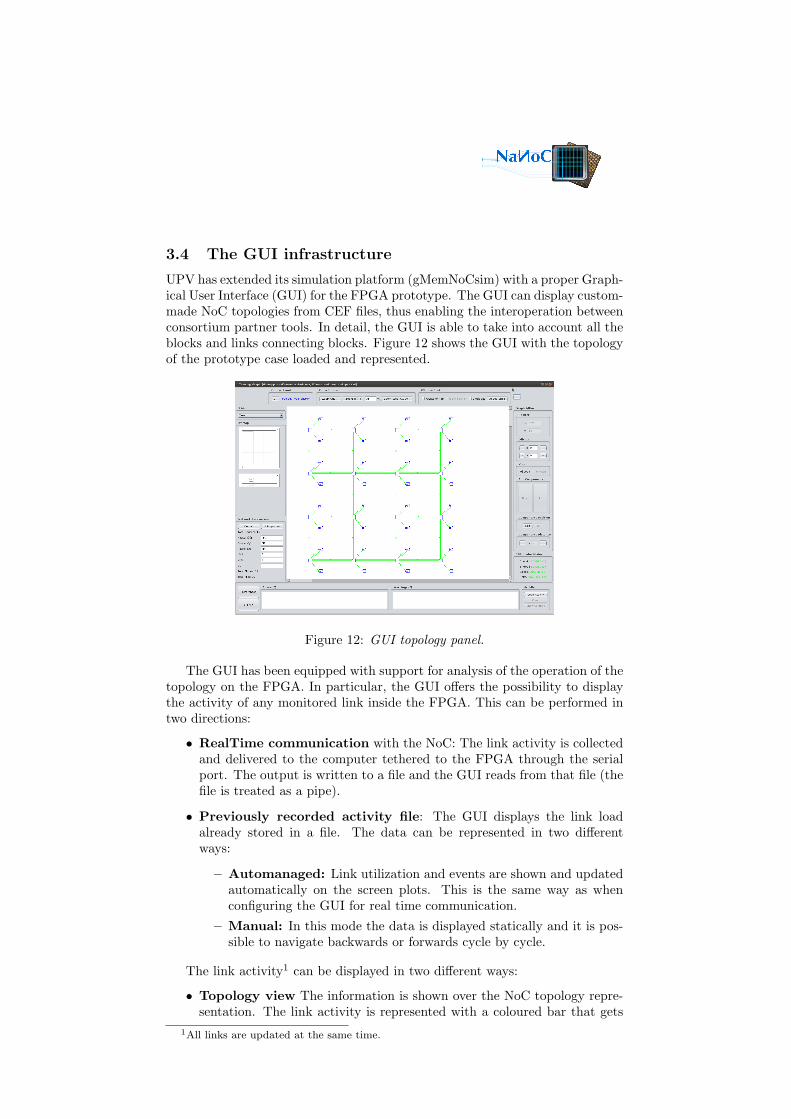
UPV has extended its simulation platform (gMemNoCsim) with a proper Graph-ical User Interface (GUI) for the FPGA prototype. The GUI can display custom-made NoC topologies from CEF files, thus enabling the interoperation betweenconsortium partner tools. In detail, the GUI is able to take into account all theblocks and links connecting blocks. Figure 12 shows the GUI with the topologyof the prototype case loaded and represented.
Figure 12: GUI topology panel.
The GUI has been equipped with support for analysis of the operation of thetopology on the FPGA. In particular, the GUI offers the possibility to displaythe activity of any monitored link inside the FPGA. This can be performed intwo directions:
• RealTime communication with the NoC: The link activity is collectedand delivered to the computer tethered to the FPGA through the serialport. The output is written to a file and the GUI reads from that file (thefile is treated as a pipe).
• Previously recorded activity file: The GUI displays the link loadalready stored in a file. The data can be represented in two differentways:
– Automanaged: Link utilization and events are shown and updatedautomatically on the screen plots. This is the same way as whenconfiguring the GUI for real time communication.
– Manual: In this mode the data is displayed statically and it is pos-sible to navigate backwards or forwards cycle by cycle.
The link activity1 can be displayed in two different ways:
• Topology view The information is shown over the NoC topology repre-sentation. The link activity is represented with a coloured bar that gets
1All links are updated at the same time.

filled and changes its color as the activity increases. Green is used for anidle link and red for a fully utilized link. An example is shown in Fig-ure 13. The percentage is also displayed in numerical format just abovethe coloured bar.
• Charts view The information is shown in a new panel with independentcharts for each link as shown in Figure 14. The number of charts to displaycan be selected in this panel, as well as the link represented in each chart.
Figure 13: GUI load at links in topology view.
Figure 14: GUI load at links in grpahs view.
The GUI has been implemented exclusively for the support of the prototypeshowcase. Extra effort was required for the proper development and communi-cation with the FPGA platform. However, the developed effort is very usefulfor the UPV team as the simulator can now be used for teaching purposes onUPV’s master courses related to on-chip interconnects.

Figure 15: The matrix multiplication at work.
3.5 The application
The MicroBlazes have been programmed in order to start their application afterthe 4x4 mesh is configured, upon flipping a physical switch on the board. Theapplication run by the MicroBlazes is a matrix multiplication consisting of theproduct of a pair of matrices. The MicroBlazes sequentially forward the re-sults to each other in a pipelined producer-consumer fashion. Each MicroBlazeperforms the multiplication of a private matrix and a matrix delivered by theprevious MicroBlaze of the sequence. Once the matrix product is computed theresulting matrix is forwarded to the next MicroBlaze. The lack of I/O interfacesand memory does not allow the implementation of more advanced applications.
The private matrix (mat private) is stored by each Microblaze into its local(pertaining to its local switch) AHB scratch memory of 4kB and it is simplyinitialized as follows:
for (row = 0; row < LINES; row ++)
for (column = 0; column < LINES; column ++)
(*mat_private)[row][column] = row + column;
Notice that the matrix size can be tuned by means of the LINES parameter.Moreover the same matrix multiplication can be set to run for a specific num-ber of times or in an endless fashion. The AHB memory is used as storageand for inter-processor communication in the application. Indeed the incomingmatrix from the previous Microblaze (mat input) is stored in the AHB mem-ory connected to the local switch. Each MicroBlaze stores its matrix productresult (mat output) into the AHB memory connected to the switch to whichthe next MicroBlaze of the sequence is connected. The first MicroBlaze of thepipeline initializes its own local AHB memory before performing the matrixproduct. Each MicroBlaze has local registers storing the address of the localAHB memory, the addreses of the remote AHB memory of the next MicroBlaze,the position within the pipeline, and the pipeline length. Figure 15 depicts theapplication at work.
The application run by each Microblaze is simply the following:

for (i = 0; i < LINES; i ++)
for (k = 0; k < LINES; k ++) {
(*mat_output)[i][k] = 0;
for (j = 0; j < LINES; j ++)
(*mat_output)[i][k]+=(*mat_input)[i][j]*(*mat_private)[j][k];
}
In order to guarantee the synchronism between the MicroBlazes, customsemaphores are implemented. Interestingly, these are purely software and donot need dedicated hardware support. Such a solution slightly increases thecomplexity of the code but clearly simplifies the hardware design effort and thearea overhead. Of course this approach is possible only since the application isfixed and known upfront; more sophisticated synchronization capabilities woulddemand hardware-level atomicity support.
The goal of these semaphores is to avoid reading the same incoming matrixmultiple times, and to avoid overwriting output matrices before the next Mi-croBlaze has been able to process them. Each MicroBlaze has been enhancedwith 4 semaphores:
• Semaphores read is stored in the local AHB memory. It is polled (andtherefore set) by the local MicroBlaze, while it is reset by the next MicroB-laze of the sequence to notify that it is available to receive new input. Assoon as polling reveals that the semaphore is reset, the local MicroBlazecan forward the matrix product result to the next MicroBlaze.
• Semaphores write is stored in the local AHB memory. Similarly to theprevious semaphore, it can be polled and set by the local MicroBlaze whileit is reset by the previous MicroBlaze of the sequence to notify that a newinput matrix is incoming.
• Semaphores readprev is stored in the AHB memory of the previous Mi-croBlaze. The current MicroBlaze resets it as soon as it has read thematrix incoming from the previous MicroBlaze.
• Semaphores writenext is stored in the AHB memory of the next Mi-croBlaze. The current MicroBlaze reset it as soon as it has forwarded thematrix product result to the next MicroBlaze.
Notice that semaphores to be polled have been placed in the local AHB memoryin order to reduce congestion in the network. Figure 16 shows the semaphoreslocation.
Since hardware support to semaphores has not been implemented, specialcare was devoted to guarantee the proper semaphore initialization. IndeedSemaphores write and Semaphores readprev needs to be respectively initial-ized to 1 and 0. Also, semaphore initialization must occur in synchronism oth-erwise the first MicroBlaze could start operations before the next MicroBlaze isactually ready. Thus, the initialization sequence progresses in reverse order withrespect to the pipeline: each MicroBlaze only initializes its own semaphores oncethe semaphores of the next MicroBlaze have been already initialized. The lastMicroBlaze of the pipeline is therefore the first allowed to initialize itself, whilethe first will be the last. This ensures that the matrix multiplication starts onlywhen all the MicroBlazes are properly initialized.
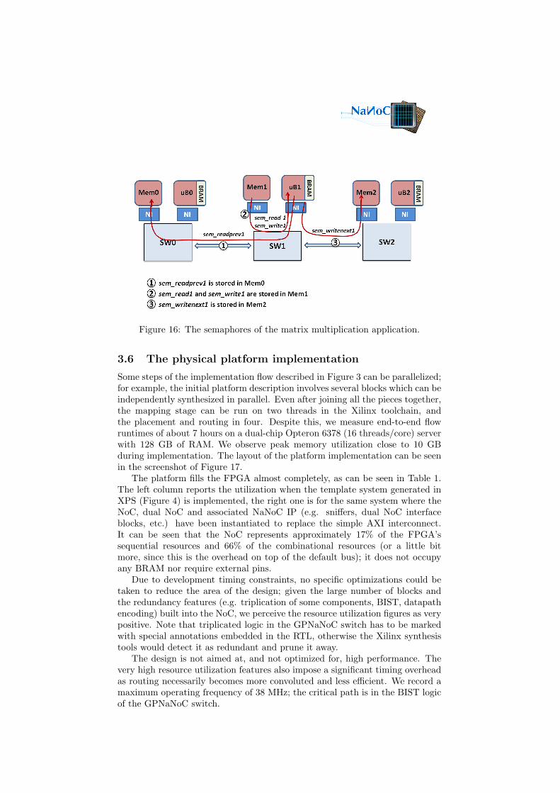
Figure 16: The semaphores of the matrix multiplication application.
3.6 The physical platform implementation
Some steps of the implementation flow described in Figure 3 can be parallelized;for example, the initial platform description involves several blocks which can beindependently synthesized in parallel. Even after joining all the pieces together,the mapping stage can be run on two threads in the Xilinx toolchain, andthe placement and routing in four. Despite this, we measure end-to-end flowruntimes of about 7 hours on a dual-chip Opteron 6378 (16 threads/core) serverwith 128 GB of RAM. We observe peak memory utilization close to 10 GBduring implementation. The layout of the platform implementation can be seenin the screenshot of Figure 17.
The platform fills the FPGA almost completely, as can be seen in Table 1.The left column reports the utilization when the template system generated inXPS (Figure 4) is implemented, the right one is for the same system where theNoC, dual NoC and associated NaNoC IP (e.g. sniffers, dual NoC interfaceblocks, etc.) have been instantiated to replace the simple AXI interconnect.It can be seen that the NoC represents approximately 17% of the FPGA’ssequential resources and 66% of the combinational resources (or a little bitmore, since this is the overhead on top of the default bus); it does not occupyany BRAM nor require external pins.
Due to development timing constraints, no specific optimizations could betaken to reduce the area of the design; given the large number of blocks andthe redundancy features (e.g. triplication of some components, BIST, datapathencoding) built into the NoC, we perceive the resource utilization figures as verypositive. Note that triplicated logic in the GPNaNoC switch has to be markedwith special annotations embedded in the RTL, otherwise the Xilinx synthesistools would detect it as redundant and prune it away.
The design is not aimed at, and not optimized for, high performance. Thevery high resource utilization features also impose a significant timing overheadas routing necessarily becomes more convoluted and less efficient. We record amaximum operating frequency of 38 MHz; the critical path is in the BIST logicof the GPNaNoC switch.
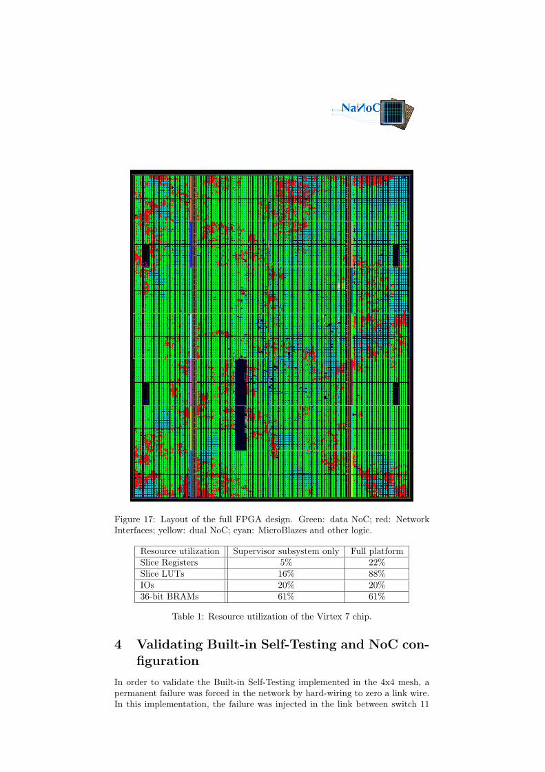
Figure 17: Layout of the full FPGA design. Green: data NoC; red: NetworkInterfaces; yellow: dual NoC; cyan: MicroBlazes and other logic.
Resource utilization Supervisor subsystem only Full platformSlice Registers 5% 22%Slice LUTs 16% 88%IOs 20% 20%36-bit BRAMs 61% 61%
Table 1: Resource utilization of the Virtex 7 chip.
4 Validating Built-in Self-Testing and NoC con-figuration
In order to validate the Built-in Self-Testing implemented in the 4x4 mesh, apermanent failure was forced in the network by hard-wiring to zero a link wire.In this implementation, the failure was injected in the link between switch 11
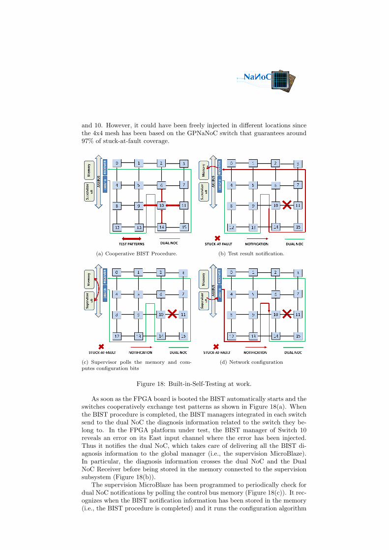
and 10. However, it could have been freely injected in different locations sincethe 4x4 mesh has been based on the GPNaNoC switch that guarantees around97% of stuck-at-fault coverage.
(a) Cooperative BIST Procedure. (b) Test result notification.
(c) Supervisor polls the memory and com-putes configuration bits
(d) Network configuration
Figure 18: Built-in-Self-Testing at work.
As soon as the FPGA board is booted the BIST automatically starts and theswitches cooperatively exchange test patterns as shown in Figure 18(a). Whenthe BIST procedure is completed, the BIST managers integrated in each switchsend to the dual NoC the diagnosis information related to the switch they be-long to. In the FPGA platform under test, the BIST manager of Switch 10reveals an error on its East input channel where the error has been injected.Thus it notifies the dual NoC, which takes care of delivering all the BIST di-agnosis information to the global manager (i.e., the supervision MicroBlaze).In particular, the diagnosis information crosses the dual NoC and the DualNoC Receiver before being stored in the memory connected to the supervisionsubsystem (Figure 18(b)).
The supervision MicroBlaze has been programmed to periodically check fordual NoC notifications by polling the control bus memory (Figure 18(c)). It rec-ognizes when the BIST notification information has been stored in the memory(i.e., the BIST procedure is completed) and it runs the configuration algorithm

described in Section 3.3. Thus, it computes configuration bits able to guaran-tee deadlock-free routes despite the failed link. The configuration bits are sentto the Dual NoC Driver through the AXI bus. They cross the dual NoC andconfigure the routing mechanism of each switch (Figure 18(d)).
4.1 Protocol for BIST notification and configuration
The 4x4 mesh is properly configured only once the configuration bits are senttwice by the supervision MicroBlaze. The exchanged information follows a so-phisticated protocol envisaged to meet multiple requirements:
• The dual NoC is a highly simplified version of the main NoC. The infor-mation travels in small packets composed of 2 or 3 flits as a function of thenotification type. Only head and tail flits are required when a notificationrelated to transient errors is delivered.
• The information must be exhaustive in order to allow the supervisionMicroBlaze to take a wide range of diagnosis and recovery actions. As anexample, it should be able to identify the kind of fault (fault type) thathas occurred (permanent or transient) and the address of the failed switch(address sender).
• The notification information should be able to pinpoint the exact locationof the error inside the switch (bist result) to enable an effective networkconfiguration.
• The protocol must be intrinsically fault tolerant to guarantee a reliablecommunication. Thus, the information is sent multiple times or encodedwithin the packets.
• The configuration bits generated by the supervision MicroBlaze mustmatch the specifications of the switch routing mechanism (Section 3.1.2).
In the case of BIST notification and configuration the protocol consists of4 phases. In the first phase, the switches notify the BIST results by means ofthree 22-bit flits with the following format:
Head:flit type(2), priority(2), address sender(8), unused(10);Body:flit type(2), fault type(2), ctrl(2), bist result(10), unused(6);Tail:flit type(2), ctrl neg(2), fault type neg(2), bist result neg(10), unused(6);Note that the tail flit contains the body information in its negated version forfault tolerance reasons.
During the second phase, the supervision MicroBlazes sends the configura-tion bits in compliance with the LBDR specification by means of three flits perswitch:
Head:flit type(2), priority(2), address receiver(8), unused(10);Body:
flit type(2), ctrl(2), lbdr configuration(18);Tail:flit type(2), lbdr configuration(20);
In the third phase, the switches forward back to the MicroBlaze the con-figuration information just received following the same above reported format.
In the last phase, the MicroBlaze checks the incoming information to en-sure that the configuration information delivered in the second phase has beencorrectly received by the switches. If the delivery is confirmed as safe, the Mi-croBlaze notifies the switches by sending for the second time a replica of thesecond phase information.
It was established that this 4-phase protocol provides the best tradeoff be-tween robustness, performance and complexity. It is however conceivable, andrelatively straightforward, to extend it further for additional resilience to faults,for example with additional request/response exchanges or additional encodingof the configuration strings. This is entirely a degree of freedom that can becustomized in the platform depending on the envisaged final application.
Once the 4 phases have been executed, the 4x4 mesh is configured and thematrix multiplication application described in Section 3.5 can run properly.
5 Validating Fault Detection and NoC Recon-figuration
Once the network has been tested and permanent faults have been detectedand tackled by the off-line configuration, the system can be still affected byrun-time transient and intermittent faults. Such faults cannot be handled byoff-line strategies as they appear and disappear unpredictably. As a result,the network has been designed as fault tolerant to satisfy the high reliabilityconstraints imposed by modern systems (see Section 3.1.2). In particular, thefault-tolerant flow control protocol (NACK/GO) is used on the data path tonotify error detection and trigger data retransmissions. Although this protocolhas been primarily designed to tackle SEUs (Single Event Upset), the system isalso able to tackle physical effects such as wear-out. Indeed wear-out effects endup in permanent faults but they are known to have a gradual onset. In practice,frequent transient faults affecting the same circuitry denote the possible onset ofa permanent fault. Before this happens, the network routing function could bemodified to exclude the affected circuit from communication traffic. NACK/GOlends itself to such a policy, since its retransmission and/or voting events may benotified to the supervision MicroBlaze which may monitor the distribution andfrequency of transient faults over time and eventually take the proper courseof recovery action. This exact policy is supported and validated by the FPGAplatform.
Physical buttons and switches of the board are connected to an on-chipGPIO controller to allow the user to interact with the platform. The physicalbuttons have been leveraged to inject transient faults in the network and validatethe above mentioned fault tolerance policy. For this purpose, a fault injectionmodule has been instantiated along the link routed from switch 4 to 5. Thismodule is connected to a physical button on the FPGA board and provides a
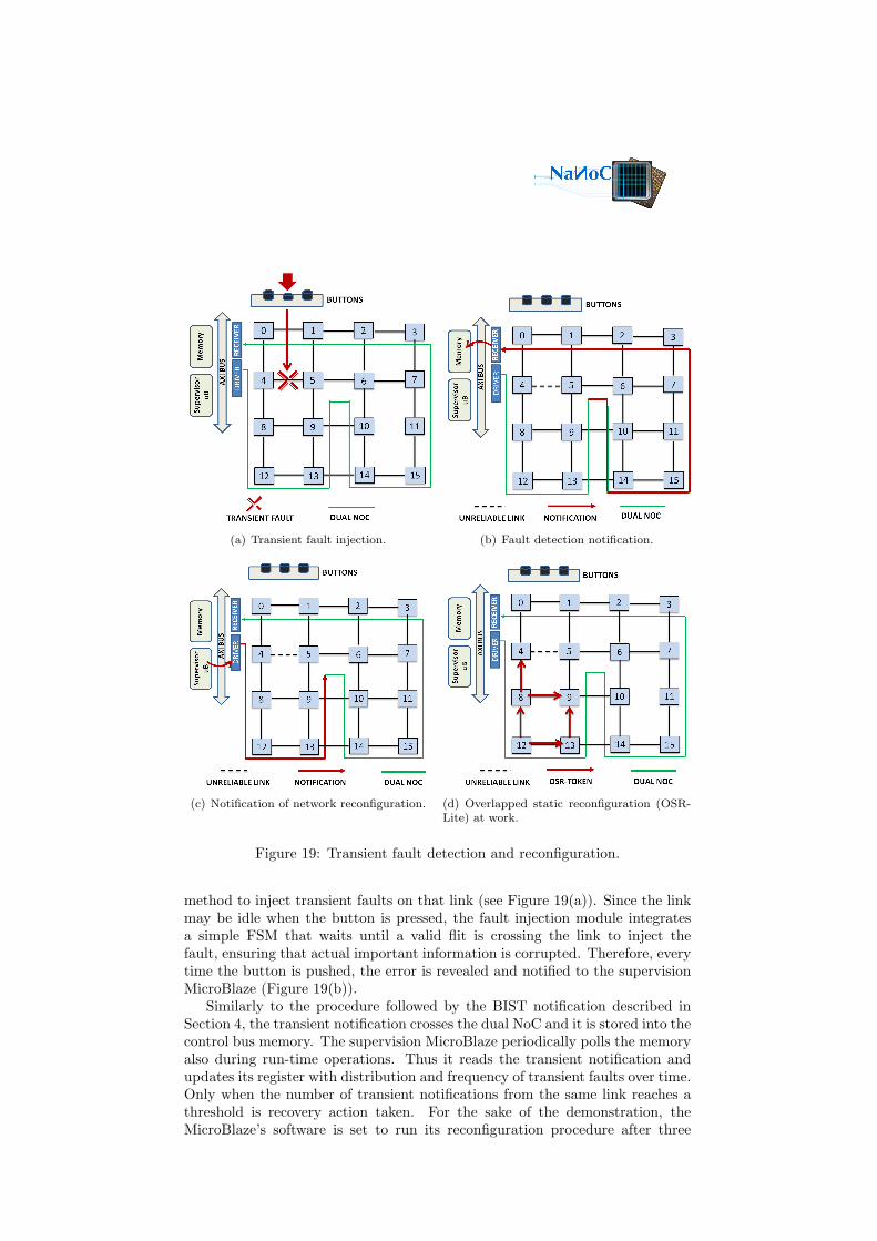
(a) Transient fault injection. (b) Fault detection notification.
(c) Notification of network reconfiguration. (d) Overlapped static reconfiguration (OSR-Lite) at work.
Figure 19: Transient fault detection and reconfiguration.
method to inject transient faults on that link (see Figure 19(a)). Since the linkmay be idle when the button is pressed, the fault injection module integratesa simple FSM that waits until a valid flit is crossing the link to inject thefault, ensuring that actual important information is corrupted. Therefore, everytime the button is pushed, the error is revealed and notified to the supervisionMicroBlaze (Figure 19(b)).
Similarly to the procedure followed by the BIST notification described inSection 4, the transient notification crosses the dual NoC and it is stored into thecontrol bus memory. The supervision MicroBlaze periodically polls the memoryalso during run-time operations. Thus it reads the transient notification andupdates its register with distribution and frequency of transient faults over time.Only when the number of transient notifications from the same link reaches athreshold is recovery action taken. For the sake of the demonstration, theMicroBlaze’s software is set to run its reconfiguration procedure after three

notifications (i.e., after the button has been pushed three times). Note thatthe 4x4 mesh at this stage is irregular since a link has been already disableddue to a previously detected permanent failure. Thus, the algorithm computesthe reconfiguration bits for this irregular network and delivers them to the dualNoC (Figure 19(c) and Section 3.3).
The new reconfiguration bits coming from the dual NoC cannot directlyupdate the existing routing strategy, as during off-line operations, since appli-cations are now running. Thus, the network implements the OSR-Lite recon-figuration mechanism which avoids stopping or draining network traffic duringthe transition from one network configuration to another. As described in Sec-tion 3.1.2, the switches of the FPGA platform start to inject tokens into thenetwork. The tokens follow the channel dependency graph of the old routingfunction and progressively drain the network from old packets, as representedin Figure 19(d).
5.1 Protocol for transient notification and reconfiguration
As described in the case of BIST notification, also transient notification andreconfiguration follow a sophisticated protocol able to meet the platformrequirements underlined in Section 4.1. The protocol consists again of 4 phases.The protocol moves to the second phase only when the switches notify multipletimes a transient fault on the same link/switch port. Otherwise, the first phaseis repeated until the notification threshold value is reached. The transientnotification is forwarded to the supervision MicroBlaze by means of two flitswith the following format:
Head:flit type(2), priority(2), address sender(8), time info(10);Tail:flit type(2), fault type(2), ctrl(2), transient position(10), unused(6);
Differently from BIST notification, the head flit contains information aboutthe error time occurrence (time info), which can be useful to compute thefrequency of the transient. The transient position field pinpoints the locationof the fault within the switch.
When the number of transient notifications reaches the threshold the secondphase starts. The MicroBlaze sends reconfiguration bits following the sameformat of the off-line configuration, previously described:
Head:flit type(2), priority(2), address receiver(8), unused(10);Body:flit type(2), ctrl(2), lbdr configuration(18);Tail:flit type(2), lbdr configuration(20);
As during configuration, the switches forward back the reconfigurationinformation to the MicroBlaze (third phase) and finally the latter sends for asecond time a replica of the reconfiguration information (fourth phase). Oncethe 4 phases have been executed, the 4x4 mesh starts to inject the OSR-Lite

tokens to drain the network and migrate to the new routing strategy.
6 Validating NoC Virtualization
0 1
4 5
8 9
12 13
2 3
6 7
10 11
14 15
MATRIX MULTIPLICATION
PROPAGATION
(a) (b)
Figure 20: Network regions before (a) and after virtualization (b). Note that thearrows indicate the logical application flow, not necessarily the route followedby packets. For case (b), the arrows are only indicative of partitioning, but thepipeline sequence is in fact shuffled for verification purposes.
The 4x4 mesh of the FPGA platform is also able to support virtualization.In order to validate such a feature, the platform is virtualized at run-time. Inparticular, the network has a single region when the operations start after theboot procedure. Thus, the same matrix multiplication application is run byall the 16 MicroBlazes and it propagates from Switch 0 to Switch 15 in a zig-zag fashion, as illustrated in Figure 20(a). Since virtualization is not in place,packets follow the best deadlock-free path available. Note that packets do notstrictly respect the arrow of Figure 20(a) but they are routed in compliancewith the actual routing strategy which takes into account also the faults ofthe considered scenario. If the user requires a virtualization, the network issplit in three regions, as represented in Figure 20(b). In this new mode, adedicated matrix multiplication application runs into each region and packetsare constrained to respect virtual boundaries.
In order to enforce virtualization at the user’s request, external interfaces arerequired. Dedicated physical switches on the board serve this purpose. Theseare directly connected to the initiator NIs of the 16 data NoC MicroBlazes(Section 3.1.1). All 16 MicroBlazes periodically check the status of the physicalswitches. When they detect a change, they transition operating mode, inter-rupting the current application, reading the address map for the new matrixmultiplication sequence of Figure 20(b), and finally running the new applica-tion.
The status of the physical switches can be polled by the supervision MicroB-laze too, through the GPIO controller. Therefore, in parallel, the software on

the supervision MicroBlaze detects the request to get into virtualized applica-tion mode (Figure 21(a)). The reconfiguration bits required to virtualize thenetwork are then computed and sent through the dual NoC (Figure 21(b)). Inparticular, the routing algorithm modifies the connectivity bits of the switchrouting functions to shape the network in three virtual regions. The tokenpropagation of the OSR Lite reconfiguration mechanism is triggered (Figure21(c)) as described in the previous section. The packets are eventually forcedto propagate within the region boundaries.
Note that the sequence of the application propagation of Figure 20(b) is onlyindicative; if the pipeline were as depicted, communication would be strictlypoint-to-point across a single hop, and virtualization would be unnecessary. Toverify its effectiveness, each of the three pipelines has been shuffled, so thatproducer-consumer traffic would tend to stray out of the geometric shape of
(a) Notification of virtualization request. (b) Notification of network reconfiguration.
(c) Overlapped static reconfiguration (OSR-Lite) at work.
Figure 21: Virtualization request and reconfiguration.
each region, if not for virtualization enforcement. As a consequence, it has beenpossible to prove that the packets do not violate the region constraints evenwhen the theoretical best deadlock-free path goes through a neighboring region.
The protocol adopted to communicate the reconfiguration bits for virtual-ization matches that for transient reconfiguration (Section 5.1). However theprotocol is 3-phase only; the first phase is missing since the reconfiguration istriggered by external physical switches instead of by a network notification.
7 Conclusions
This deliverable reports on the prototyping of a 16-core homogeneous multi-core processor with a fault-tolerant, runtime reconfigurable and dynamicallyvirtualizable on-chip network. The prototyped system has been successfullyvalidated in its capability of boot-time testing and configuration, transient orintermittent fault detection, runtime reconfiguration of the routing function,and dynamic partitioning and isolation. The FPGA prototype is the outcomeof a tight cooperation between key NaNoC partners: UNIFE, INOCS, UPV, andSIMULA, to such an extent that their contributions is currently indivisible. Thevalidated NoC prototype is a key enabler for the future evolution of embeddedsystems. First, it enables the integration of multiple software functions on asingle multi- and many-core processor (multifunction integration). This is themost efficient way of utilizing the available computing power. Ultimately, theNaNoC project is a milestone in the direction of mixed-criticality multifunctionintegration. Second, NaNoC design methods enable advanced forms of platformcontrol, especially power management and thermal control. In fact, parts of thenetwork can be easily powered off, while preserving its global functionality andguaranteeing safe transitions between network configurations. Third, NaNoCtechnology paves the way for an effective graceful degradation of the systemin the presence of permanent and intermittent faults. The routing functioncan be reconfigured at runtime to avoid faulty links and switches. Finally,a comprehensive reliability framework has been set into place, from switch-level to network-level, while covering all design aspects (e.g., reliable controlsignaling) and effectively co-optimizing different architectural features together(fault-tolerance, testing, runtime reconfiguration, control signaling).
References
[1] S.Rodrigo et Al. ”Addressing Manufacturing Challenges with Cost-EffectiveFault Tolerant Routing”, NOCS 2010, pp.35-32, 2010.
[2] A.Ghiribaldi, A.Strano, M.Favalli, D.Bertozzi ”Power Efficiency of SwitchArchitecture Extensions for Fault Tolerant NoC Design“ IGCC’12, 2012,California, USA
[3] A. Pullini, et Al. ”Fault Tolerance Overhead in Network-on-Chip FlowControl Schemes,” SBCCI, Brazil, 2005, pp. 224-229
[4] Raik J., Govind, V., Ubar R. ”An external test approach for network-on-a-chip switches”. ATS06, 2006.

[5] S.Terenzi, A.Strano, D.Bertozzi, ”Optimizing Built-In Pseudo-Random Self-Testing for Network-on-Chip Switches”, INA-OCMC 2012.
[6] A. Ghiribaldi, D. Ludovici, M. Favalli, D. Bertozzi. ”System-Level Infras-tructure for Boot-time Testing and Configuration of Networks-on-Chip withProgrammable Routing Logic.”, VLSI-SoC, 2011.
[7] A.Strano, F.Trivino, Jose L. Sanchez, Jose Flich, D.Bertozzi ”OSR-Lite:Fast and Deadlock-Free NoC Reconguration Framework”, SAMOS 2012.