ifip aict 373 - tri-mode operation for noise reduction and ... jiao and volkan kursun department of...
TRANSCRIPT
J.L. Ayala, D. Atienza, and R. Reis (Eds.): VLSI-SoC 2010, IFIP AICT 373, pp. 258–290, 2012. © IFIP International Federation for Information Processing 2012
Tri-mode Operation for Noise Reduction and Data Preservation in Low-Leakage
Multi-Threshold CMOS Circuits
Hailong Jiao and Volkan Kursun
Department of Electronic and Computer Engineering The Hong Kong University of Science and Technology
Clear Water Bay, Kowloon, Hong Kong {jiaohl,eekursun}@ust.hk
Abstract. Multi-threshold CMOS (MTCMOS) is the most widely used circuit technique for suppressing subthreshold leakage currents in idle circuits. When a conventional MTCMOS circuit transitions from SLEEP mode to ACTIVE mode, voltages of power and ground distribution networks are disturbed. Mode transition noise phenomenon in MTCMOS circuits is examined in this chapter. An MTCMOS circuit technique with three operating modes (tri-mode) is described for noise suppression during activation events. A threshold voltage tuning methodology is presented to further alleviate the mode transition noise with smaller sleep transistors in MTCMOS circuits. Alternative applications of tri-mode MTCMOS for data preservation and leakage power reduction in idle memory elements are also discussed.
Keywords: Mode transition noise, tri-mode MTCMOS, data preserving SLEEP mode, forward body bias, sleep transistor miniaturization, subthreshold leakage currents, leakage power consumption, activation noise, activation delay, electrical quality.
1 Introduction
Leakage power consumption is an important concern in modern nanoscale integrated circuits [1] – [48]. Subthreshold leakage currents of integrated circuits increase exponentially with the reduced threshold voltages of transistors in advanced CMOS technologies. High performance integrated circuits (such as microprocessors) rarely operate with full workload [2]. Most of the circuit blocks on a microprocessor are typically idle for long periods during normal operation [1]. Leakage currents produced by these idle circuit blocks contribute significantly to the total power consumption of a chip. Furthermore, mobile devices such as smart phones and tablet computers experience long idle periods where significant energy is consumed due to leakage currents. Leakage currents drain the battery in portable devices. Suppressing subthreshold leakage currents in large scale integrated circuits is essential both for facilitating the proliferation of portable electronics and for green computing.
Tri-mode Operation for Noise Reduction and Data Preservation 259
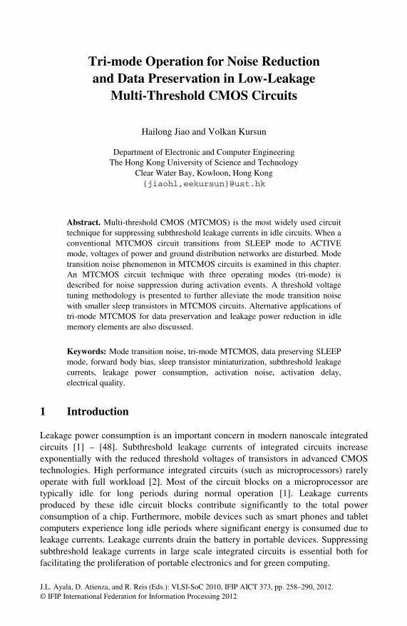
MTCMOS is the most commonly used leakage power suppression technique in state-of-the-art integrated circuits [1] – [36]. In an MTCMOS circuit, high threshold voltage (high-|Vth|) sleep transistors (header and/or footer) are used to cut off the power supply and/or the ground connections to an idle low threshold voltage (low-|Vth|) circuit block as illustrated in Fig. 1. In a power-gated MTCMOS circuit, a high-|Vth| header is attached between the chip power distribution network (directly connected to the power supply) and a virtual power line (connected to the low threshold voltage circuit block) as shown in Fig. 1(a). Alternatively, in a ground-gated MTCMOS circuit, a high-|Vth| footer is inserted between the chip ground distribution network and a virtual ground line (connected to the low threshold voltage circuit block) as shown in Fig. 1(b). In a power and ground gated MTCMOS circuit, both a high-|Vth| header and a high-|Vth| footer are utilized to block access to the chip power and ground distribution networks, as illustrated in Fig. 1(c). In SLEEP mode, the header and footer are cut off to lower the subthreshold leakage currents in an idle circuit block. Alternatively, in ACTIVE mode, the header and footer are activated to resume normal circuit operation with high performance.
(a) (b)
(c)
Fig. 1. Standard MTCMOS circuits in SLEEP mode. (a) Power-gated MTCMOS circuit. (b) Ground-gated MTCMOS circuit. (c) Power and ground gated MTCMOS circuit. High-|Vth| sleep transistors are represented with a thick line in the channel region.
Multiple autonomous power and ground gated circuit domains are typically utilized for effective control of leakage power consumption in MTCMOS circuits [2],
260 H. Jiao and V. Kursun
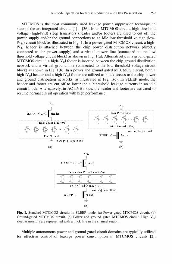
[23] – [27]. When low-|Vth| logic blocks transition from SLEEP mode to ACTIVE mode, significant voltage fluctuations occur on the real power and ground distribution networks in an MTCMOS circuit, as illustrated in Fig. 2. The real power and ground wires are shared by all the circuit blocks on a chip. The mode transition noise produced by an awakening MTCMOS circuit block is transferred through the shared power and ground distribution networks to the other active circuit blocks across an integrated circuit. An awakening circuit block thereby acts as an aggressor in a multi-domain MTCMOS circuit. The active circuit blocks become victims of the noise produced by an awakening aggressor. The voltage levels of the internal nodes of active logic circuits are disturbed. Provided that the amplitude of mode transition noise is significantly high, the logic states of the internal nodes can be flipped. The active segments of an integrated circuit may malfunction due to an awakening circuit block. Furthermore, the voltage fluctuations on internal nodes cause short circuit currents in the active logic gates. The propagation delay and the dynamic switching power consumption of active logic blocks can be thereby increased [6], [28]. The noise margins of logic gates can also be temporarily reduced by the mode transition noise. The reliabilities of the active logic blocks are thereby degraded in the vicinity of an awakening MTCMOS circuit. With smaller device dimensions, lower power supply voltage, and exacerbated process variations, noise immunity of CMOS circuits is significantly weakened in each new CMOS technology generation. Mode transition noise is expected to become an increasingly important reliability issue in future deeply scaled multi-domain MTCMOS circuits with narrower noise margins [2], [23] – [26], [49].
Fig. 2. Power and ground bouncing noise generated by an awakening autonomous power and ground gated circuit block in a multi-domain MTCMOS circuit [6]. High-|Vth| sleep transistors are represented with a thick line in the channel region. SLEEP1: 0 → VDD. SLEEP2 = SLEEP3 = VDD.
Low-leakage MTCMOS circuits with three operational modes (tri-mode) are described in this chapter for activation noise reduction and data preservation. As a case study, threshold voltage tuning techniques are examined to suppress mode

Tri-mode Operation for Noise Reduction and Data Preservation 261
transition noise with smaller sleep transistors and shorter activation delay in ground-gated tri-mode MTCMOS integrated circuits. The principal mechanisms of noise and sleep transistor size reduction with the threshold voltage tuning techniques are discussed.
This chapter is organized as follows. The generation of mode transition noise in MTCMOS circuits is described in Section 2. Noise-aware tri-mode MTCMOS circuit technique is reviewed in Section 3. Threshold voltage tuning in tri-mode MTCMOS circuits is discussed. Application of tri-mode MTCMOS for data preservation and leakage reduction in memory elements is presented in Section 4. A case study on 32-bit tri-mode MTCMOS Brent-Kung adder design is provided in Section 5. Tradeoffs among mode transition noise, activation delay, leakage power consumption, active power consumption, and layout area in MTCMOS circuits are discussed. A summary of this chapter is given in Section 6.
2 Mode Transition Noise
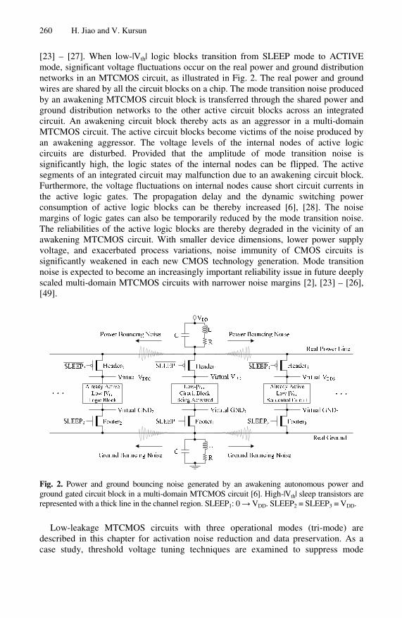
Mode transition noise (power and ground bouncing noise) is caused by the resistive and inductive parasitics of on-chip power distribution network, off-chip bonding wires, and pins of package. The package parasitic impedances typically play the most important role in the generation of mode transition noise [6] – [13], [49]. A conventional MTCMOS circuit with package parasitics is illustrated in Fig. 3 [6]. R, L, and C are the parasitic resistor, parasitic inductor, and parasitic capacitor of the package, respectively. Parasitic capacitors of the header, the low-|Vth| transistors, and the virtual power line are lumped in C1. C2 represents the parasitic capacitors of the footer, the low-|Vth| transistors, and the virtual ground line. C3 and C4 are the lumped capacitors of the low-|Vth| transistors attached to the internal nodes “A” and “B”, respectively.
When the MTCMOS circuit block is in ACTIVE mode, both the header and the footer are turned on. The virtual power and ground lines are maintained at ~VDD and ~0V, respectively. The effective supply voltage experienced by the low-|Vth| circuitry is approximately equal to the power supply voltage VDD. The MTCMOS circuit thereby operates with high performance in ACTIVE mode.
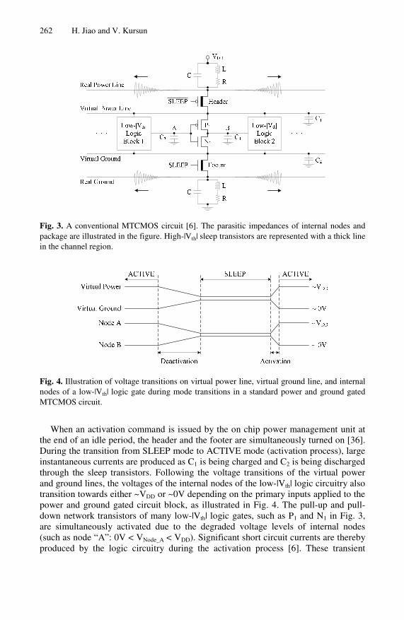
An idle MTCMOS circuit block is placed into a low-leakage SLEEP mode by turning off the header and the footer. During the transition from ACTIVE mode to SLEEP mode (deactivation process), C1 is discharged slowly from an initial voltage of ~VDD to an intermediate voltage level between VDD and 0V by the leakage currents through the low-|Vth| logic gates and the high-|Vth| footer, as illustrated in Fig. 4. Similarly, C2 is charged slowly from ~0V to an intermediate voltage level between VDD and 0V by the leakage currents through the low-|Vth| logic gates and the high-|Vth| header. Following the transitions of virtual power and ground line voltages, the internal nodes of the low-|Vth| circuit block also transition to intermediate steady-state voltage levels between VDD and 0V by the leakage currents through the sleep transistors. The deactivation noise produced during ACTIVE to SLEEP mode transitions is typically insignificant [24], [35].
262 H. Jiao and V. Kursun
Fig. 3. A conventional MTCMOS circuit [6]. The parasitic impedances of internal nodes and package are illustrated in the figure. High-|Vth| sleep transistors are represented with a thick line in the channel region.
Fig. 4. Illustration of voltage transitions on virtual power line, virtual ground line, and internal nodes of a low-|Vth| logic gate during mode transitions in a standard power and ground gated MTCMOS circuit.
When an activation command is issued by the on chip power management unit at the end of an idle period, the header and the footer are simultaneously turned on [36]. During the transition from SLEEP mode to ACTIVE mode (activation process), large instantaneous currents are produced as C1 is being charged and C2 is being discharged through the sleep transistors. Following the voltage transitions of the virtual power and ground lines, the voltages of the internal nodes of the low-|Vth| logic circuitry also transition towards either ~VDD or ~0V depending on the primary inputs applied to the power and ground gated circuit block, as illustrated in Fig. 4. The pull-up and pull-down network transistors of many low-|Vth| logic gates, such as P1 and N1 in Fig. 3, are simultaneously activated due to the degraded voltage levels of internal nodes (such as node “A”: 0V < VNode_A < VDD). Significant short circuit currents are thereby produced by the logic circuitry during the activation process [6]. These transient
Tri-mode Operation for Noise Reduction and Data Preservation 263
charging, discharging, and short circuit currents flow through the package parasitic impedances. The voltages of power and ground distribution networks are thereby disturbed.
The intensity of voltage disturbance is related to the rate of change of instantaneous current (dI/dt) conducted by sleep transistors during an activation event. The rate of change of instantaneous current is primarily determined by the power supply voltage, the size of sleep transistors, the amount of charge that is transferred through sleep transistors, and the voltage swing of virtual lines during activation events [6]. The peak amplitude of mode transition noise is increased with a higher supply voltage and a higher voltage swing on the virtual lines. Larger sleep transistors are desirable to achieve higher speed by lowering the resistive voltage drop across sleep transistors in an active MTCMOS circuit. Larger sleep transistors, however, also cause stronger current surges during mode transitions, thereby increasing the bouncing noise induced on the power and ground distribution networks. The steady-state SLEEP-mode voltages of the internal nodes and the delay of SLEEP-to-ACTIVE mode transition determine the intensity and duration of short circuit currents that are produced by the low-|Vth| transistors during a wake-up event. Higher and longer short circuit currents cause stronger current surges through sleep transistors, thereby exacerbating the noise produced during SLEEP to ACTIVE mode transitions.
3 Tri-mode MTCMOS Circuits
Various circuit techniques are described in literature to suppress power and ground bouncing noise produced by MTCMOS circuits during activation events [4] – [20]. A specialized low-noise MTCMOS circuit technique with three operational modes (tri-mode) is described in this section. A threshold voltage tuning methodology is also introduced to further reduce the activation noise with smaller sleep transistors and shorter delay in a tri-mode MTCMOS circuit. The power and ground gated tri-mode MTCMOS circuit techniques are introduced in Section 3.1. The threshold voltage tuning technique based on forward body bias is presented in Section 3.2.
3.1 Power and Ground Gated Tri-mode MTCMOS
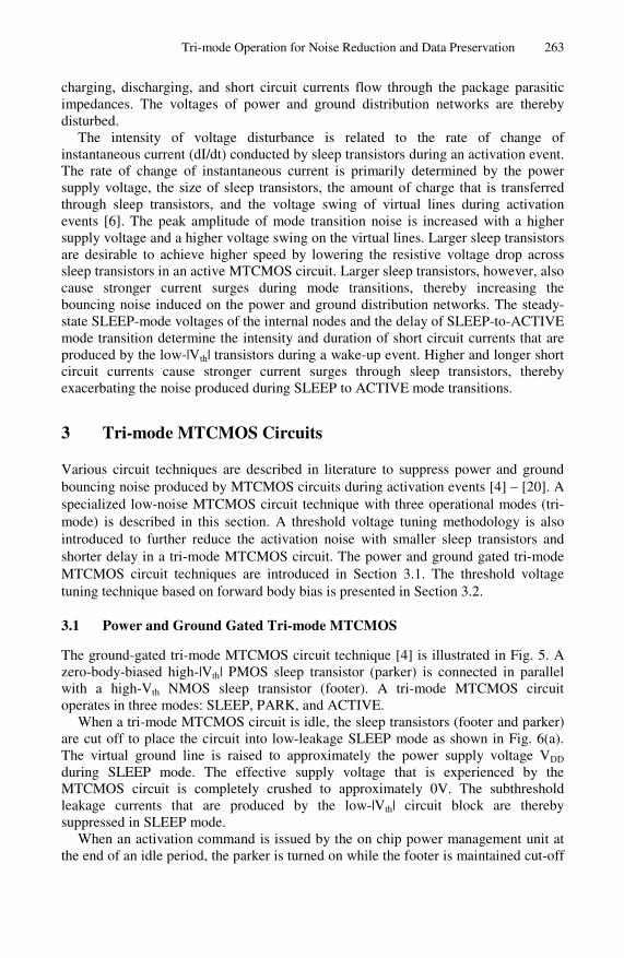
The ground-gated tri-mode MTCMOS circuit technique [4] is illustrated in Fig. 5. A zero-body-biased high-|Vth| PMOS sleep transistor (parker) is connected in parallel with a high-Vth NMOS sleep transistor (footer). A tri-mode MTCMOS circuit operates in three modes: SLEEP, PARK, and ACTIVE.
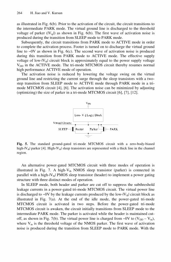
When a tri-mode MTCMOS circuit is idle, the sleep transistors (footer and parker) are cut off to place the circuit into low-leakage SLEEP mode as shown in Fig. 6(a). The virtual ground line is raised to approximately the power supply voltage VDD during SLEEP mode. The effective supply voltage that is experienced by the MTCMOS circuit is completely crushed to approximately 0V. The subthreshold leakage currents that are produced by the low-|Vth| circuit block are thereby suppressed in SLEEP mode.
When an activation command is issued by the on chip power management unit at the end of an idle period, the parker is turned on while the footer is maintained cut-off
264 H. Jiao and V. Kursun
as illustrated in Fig. 6(b). Prior to the activation of the circuit, the circuit transitions to the intermediate PARK mode. The virtual ground line is discharged to the threshold voltage of parker (|Vtp|) as shown in Fig. 6(b). The first wave of activation noise is produced during the transition from SLEEP mode to PARK mode.
Subsequently, the circuit transitions from PARK mode to ACTIVE mode in order to complete the activation process. Footer is turned on to discharge the virtual ground line to ~0V as shown in Fig. 6(c). The second wave of activation noise is produced during this transition from PARK mode to ACTIVE mode. The effective supply voltage of low-|Vth| circuit block is approximately equal to the power supply voltage VDD in the ACTIVE mode. The tri-mode MTCMOS circuit thereby resumes normal high performance ACTIVE mode of operation.
The activation noise is reduced by lowering the voltage swing on the virtual ground line and restricting the current surge through the sleep transistors with a two-step transition from SLEEP mode to ACTIVE mode through PARK mode in a tri-mode MTCMOS circuit [4], [6]. The activation noise can be minimized by adjusting (optimizing) the size of parker in a tri-mode MTCMOS circuit [6], [7], [12].
Fig. 5. The standard ground-gated tri-mode MTCMOS circuit with a zero-body-biased high-|Vth| parker [4]. High-|Vth| sleep transistors are represented with a thick line in the channel region.
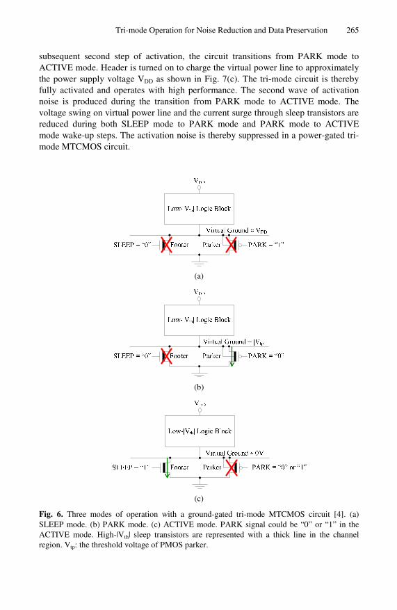
An alternative power-gated MTCMOS circuit with three modes of operation is illustrated in Fig. 7. A high-Vth NMOS sleep transistor (parker) is connected in parallel with a high-|Vth| PMOS sleep transistor (header) to implement a power gating structure with three distinct modes of operation.
In SLEEP mode, both header and parker are cut off to suppress the subthreshold leakage currents in a power-gated tri-mode MTCMOS circuit. The virtual power line is discharged to ~0V by the leakage currents produced by the low-|Vth| circuit block as illustrated in Fig. 7(a). At the end of the idle mode, the power-gated tri-mode MTCMOS circuit is activated in two steps. Before the power-gated tri-mode MTCMOS circuit is awaken, the circuit initially transitions from SLEEP mode to the intermediate PARK mode. The parker is activated while the header is maintained cut-off, as shown in Fig. 7(b). The virtual power line is charged from ~0V to (VDD – Vtn), where Vtn is the threshold voltage of the NMOS parker. The first wave of activation noise is produced during the transition from SLEEP mode to PARK mode. With the
Tri-mode Operation for Noise Reduction and Data Preservation 265
subsequent second step of activation, the circuit transitions from PARK mode to ACTIVE mode. Header is turned on to charge the virtual power line to approximately the power supply voltage VDD as shown in Fig. 7(c). The tri-mode circuit is thereby fully activated and operates with high performance. The second wave of activation noise is produced during the transition from PARK mode to ACTIVE mode. The voltage swing on virtual power line and the current surge through sleep transistors are reduced during both SLEEP mode to PARK mode and PARK mode to ACTIVE mode wake-up steps. The activation noise is thereby suppressed in a power-gated tri-mode MTCMOS circuit.
(a)
(b)
(c)
Fig. 6. Three modes of operation with a ground-gated tri-mode MTCMOS circuit [4]. (a) SLEEP mode. (b) PARK mode. (c) ACTIVE mode. PARK signal could be “0” or “1” in the ACTIVE mode. High-|Vth| sleep transistors are represented with a thick line in the channel region. Vtp: the threshold voltage of PMOS parker.
266 H. Jiao and V. Kursun
(a)
(b)
Low-|Vth| Logic Block
Parker
VDD
Real Ground
Virtual Power ≈ VDD
SLEEP = “0” PARK = “0” or “1”Header
(c)
Fig. 7. Three modes of operation with a power-gated tri-mode MTCMOS circuit. (a) SLEEP mode. (b) PARK mode. (c) ACTIVE mode. PARK signal could be “0” or “1” in the ACTIVE mode. High-|Vth| sleep transistors are represented with a thick line in the channel region. Vtn: the threshold voltage of NMOS parker.
3.2 Tri-mode MTCMOS with Threshold Voltage Tuning
Tri-mode MTCMOS circuit technique is effective for suppressing mode transition noise as compared to the standard power and/or ground gated MTCMOS circuits as described in Section 3.1. The optimum parker size that minimizes the activation noise is however typically large, thereby causing significant area and mode transition energy overheads in a tri-mode MTCMOS circuit [7] – [9], [12]. Furthermore, due to
Tri-mode Operation for Noise Reduction and Data Preservation 267
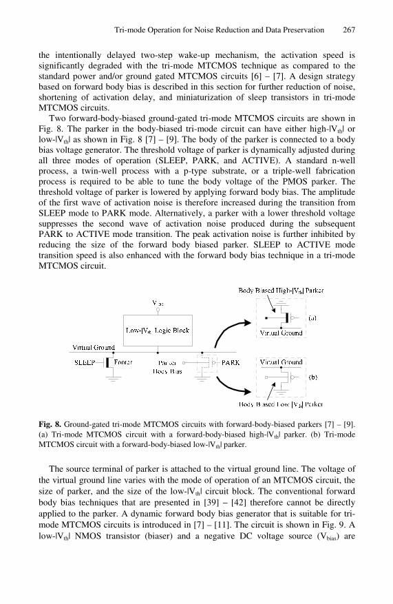
the intentionally delayed two-step wake-up mechanism, the activation speed is significantly degraded with the tri-mode MTCMOS technique as compared to the standard power and/or ground gated MTCMOS circuits [6] – [7]. A design strategy based on forward body bias is described in this section for further reduction of noise, shortening of activation delay, and miniaturization of sleep transistors in tri-mode MTCMOS circuits.
Two forward-body-biased ground-gated tri-mode MTCMOS circuits are shown in Fig. 8. The parker in the body-biased tri-mode circuit can have either high-|Vth| or low-|Vth| as shown in Fig. 8 [7] – [9]. The body of the parker is connected to a body bias voltage generator. The threshold voltage of parker is dynamically adjusted during all three modes of operation (SLEEP, PARK, and ACTIVE). A standard n-well process, a twin-well process with a p-type substrate, or a triple-well fabrication process is required to be able to tune the body voltage of the PMOS parker. The threshold voltage of parker is lowered by applying forward body bias. The amplitude of the first wave of activation noise is therefore increased during the transition from SLEEP mode to PARK mode. Alternatively, a parker with a lower threshold voltage suppresses the second wave of activation noise produced during the subsequent PARK to ACTIVE mode transition. The peak activation noise is further inhibited by reducing the size of the forward body biased parker. SLEEP to ACTIVE mode transition speed is also enhanced with the forward body bias technique in a tri-mode MTCMOS circuit.
Fig. 8. Ground-gated tri-mode MTCMOS circuits with forward-body-biased parkers [7] – [9]. (a) Tri-mode MTCMOS circuit with a forward-body-biased high-|Vth| parker. (b) Tri-mode MTCMOS circuit with a forward-body-biased low-|Vth| parker.
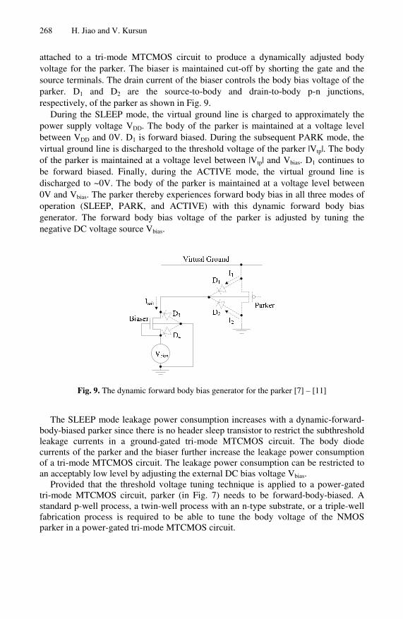
The source terminal of parker is attached to the virtual ground line. The voltage of the virtual ground line varies with the mode of operation of an MTCMOS circuit, the size of parker, and the size of the low-|Vth| circuit block. The conventional forward body bias techniques that are presented in [39] – [42] therefore cannot be directly applied to the parker. A dynamic forward body bias generator that is suitable for tri-mode MTCMOS circuits is introduced in [7] – [11]. The circuit is shown in Fig. 9. A low-|Vth| NMOS transistor (biaser) and a negative DC voltage source (Vbias) are
268 H. Jiao and V. Kursun
attached to a tri-mode MTCMOS circuit to produce a dynamically adjusted body voltage for the parker. The biaser is maintained cut-off by shorting the gate and the source terminals. The drain current of the biaser controls the body bias voltage of the parker. D1 and D2 are the source-to-body and drain-to-body p-n junctions, respectively, of the parker as shown in Fig. 9.
During the SLEEP mode, the virtual ground line is charged to approximately the power supply voltage VDD. The body of the parker is maintained at a voltage level between VDD and 0V. D1 is forward biased. During the subsequent PARK mode, the virtual ground line is discharged to the threshold voltage of the parker |Vtp|. The body of the parker is maintained at a voltage level between |Vtp| and Vbias. D1 continues to be forward biased. Finally, during the ACTIVE mode, the virtual ground line is discharged to ~0V. The body of the parker is maintained at a voltage level between 0V and Vbias. The parker thereby experiences forward body bias in all three modes of operation (SLEEP, PARK, and ACTIVE) with this dynamic forward body bias generator. The forward body bias voltage of the parker is adjusted by tuning the negative DC voltage source Vbias.
Fig. 9. The dynamic forward body bias generator for the parker [7] – [11]
The SLEEP mode leakage power consumption increases with a dynamic-forward-body-biased parker since there is no header sleep transistor to restrict the subthreshold leakage currents in a ground-gated tri-mode MTCMOS circuit. The body diode currents of the parker and the biaser further increase the leakage power consumption of a tri-mode MTCMOS circuit. The leakage power consumption can be restricted to an acceptably low level by adjusting the external DC bias voltage Vbias.
Provided that the threshold voltage tuning technique is applied to a power-gated tri-mode MTCMOS circuit, parker (in Fig. 7) needs to be forward-body-biased. A standard p-well process, a twin-well process with an n-type substrate, or a triple-well fabrication process is required to be able to tune the body voltage of the NMOS parker in a power-gated tri-mode MTCMOS circuit.
Tri-mode Operation for Noise Reduction and Data Preservation 269
4 Low-Leakage Tri-mode MTCMOS Memory Elements
Data preservation is typically a critical requirement of leakage reduction techniques applicable to memory elements. A low-leakage data retention SLEEP mode is desirable for energy-efficiency in modern nanoscale sequential circuits and static random access memory arrays. If the standard MTCMOS techniques (illustrated in Fig. 1) are directly applied to memory elements, the logic states of the circuits are lost in SLEEP mode. The retrieval of the previously stored data for post-sleep system state restoration costs significant energy and timing overheads when the power and/or ground gated memory circuits are activated [10], [11]. A low leakage SLEEP mode with data preservation capability is, therefore, critical for achieving truly energy efficient MTCMOS data storage elements such as flip-flops and static random access memory arrays [3], [10], [11], [29] – [35].
In addition to utilization for effective mode transition noise suppression, tri-mode MTCMOS technique can also be used to implement a low-leakage data preserving SLEEP mode in memory elements. Applications of the tri-mode MTCMOS technique to sequential circuits and static memory arrays are introduced in this section. Tri-mode MTCMOS flip-flops are presented in Section 4.1. Tri-mode MTCMOS static random access memory arrays are discussed in Section 4.2.
4.1 Sequential Tri-mode MTCMOS Circuits
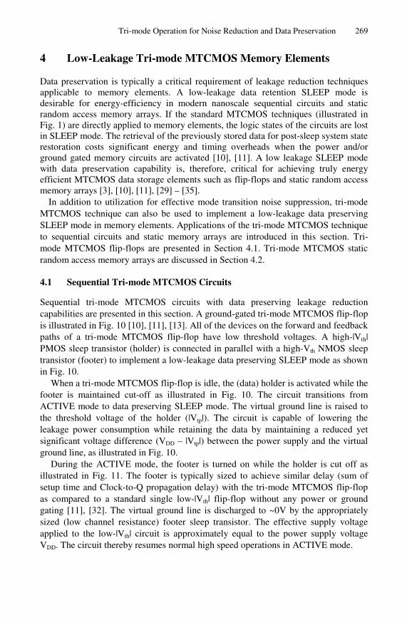
Sequential tri-mode MTCMOS circuits with data preserving leakage reduction capabilities are presented in this section. A ground-gated tri-mode MTCMOS flip-flop is illustrated in Fig. 10 [10], [11], [13]. All of the devices on the forward and feedback paths of a tri-mode MTCMOS flip-flop have low threshold voltages. A high-|Vth| PMOS sleep transistor (holder) is connected in parallel with a high-Vth NMOS sleep transistor (footer) to implement a low-leakage data preserving SLEEP mode as shown in Fig. 10.
When a tri-mode MTCMOS flip-flop is idle, the (data) holder is activated while the footer is maintained cut-off as illustrated in Fig. 10. The circuit transitions from ACTIVE mode to data preserving SLEEP mode. The virtual ground line is raised to the threshold voltage of the holder (|Vtp|). The circuit is capable of lowering the leakage power consumption while retaining the data by maintaining a reduced yet significant voltage difference (VDD – |Vtp|) between the power supply and the virtual ground line, as illustrated in Fig. 10.
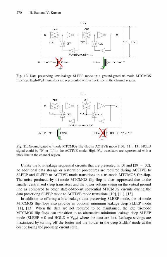
During the ACTIVE mode, the footer is turned on while the holder is cut off as illustrated in Fig. 11. The footer is typically sized to achieve similar delay (sum of setup time and Clock-to-Q propagation delay) with the tri-mode MTCMOS flip-flop as compared to a standard single low-|Vth| flip-flop without any power or ground gating [11], [32]. The virtual ground line is discharged to ~0V by the appropriately sized (low channel resistance) footer sleep transistor. The effective supply voltage applied to the low-|Vth| circuit is approximately equal to the power supply voltage VDD. The circuit thereby resumes normal high speed operations in ACTIVE mode.
270 H. Jiao and V. Kursun
Fig. 10. Data preserving low-leakage SLEEP mode in a ground-gated tri-mode MTCMOS flip-flop. High-|Vth| transistors are represented with a thick line in the channel region.
Fig. 11. Ground-gated tri-mode MTCMOS flip-flop in ACTIVE mode [10], [11], [13]. HOLD signal could be “0” or “1” in the ACTIVE mode. High-|Vth| transistors are represented with a thick line in the channel region.
Unlike the low-leakage sequential circuits that are presented in [3] and [29] – [32], no additional data storage or restoration procedures are required during ACTIVE to SLEEP and SLEEP to ACTIVE mode transitions in a tri-mode MTCMOS flip-flop. The noise produced by tri-mode MTCMOS flip-flop is also suppressed due to the smaller centralized sleep transistors and the lower voltage swing on the virtual ground line as compared to other state-of-the-art sequential MTCMOS circuits during the data preserving SLEEP mode to ACTIVE mode transitions [10], [11], [13].
In addition to offering a low-leakage data preserving SLEEP mode, the tri-mode MTCMOS flip-flops also provide an optional minimum leakage deep SLEEP mode [11], [13]. When the data are not required to be maintained, the idle tri-mode MTCMOS flip-flops can transition to an alternative minimum leakage deep SLEEP mode (SLEEP = 0 and HOLD = VDD) where the data are lost. Leakage savings are maximized by turning off the footer and the holder in the deep SLEEP mode at the cost of losing the pre-sleep circuit state.
Tri-mode Operation for Noise Reduction and Data Preservation 271
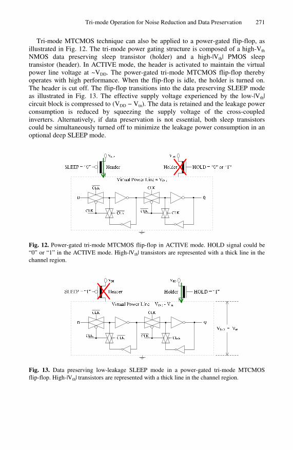
Tri-mode MTCMOS technique can also be applied to a power-gated flip-flop, as illustrated in Fig. 12. The tri-mode power gating structure is composed of a high-Vth NMOS data preserving sleep transistor (holder) and a high-|Vth| PMOS sleep transistor (header). In ACTIVE mode, the header is activated to maintain the virtual power line voltage at ~VDD. The power-gated tri-mode MTCMOS flip-flop thereby operates with high performance. When the flip-flop is idle, the holder is turned on. The header is cut off. The flip-flop transitions into the data preserving SLEEP mode as illustrated in Fig. 13. The effective supply voltage experienced by the low-|Vth| circuit block is compressed to (VDD − Vtn). The data is retained and the leakage power consumption is reduced by squeezing the supply voltage of the cross-coupled inverters. Alternatively, if data preservation is not essential, both sleep transistors could be simultaneously turned off to minimize the leakage power consumption in an optional deep SLEEP mode.
Fig. 12. Power-gated tri-mode MTCMOS flip-flop in ACTIVE mode. HOLD signal could be “0” or “1” in the ACTIVE mode. High-|Vth| transistors are represented with a thick line in the channel region.
Fig. 13. Data preserving low-leakage SLEEP mode in a power-gated tri-mode MTCMOS flip-flop. High-|Vth| transistors are represented with a thick line in the channel region.
272 H. Jiao and V. Kursun
4.2 Tri-mode MTCMOS Memory Arrays
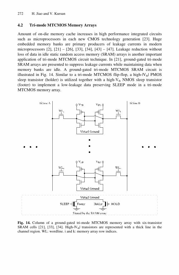
Amount of on-die memory cache increases in high performance integrated circuits such as microprocessors in each new CMOS technology generation [23]. Huge embedded memory banks are primary producers of leakage currents in modern microprocessors [2], [21] – [26], [33], [34], [43] – [47]. Leakage reduction without loss of data in idle static random access memory (SRAM) arrays is another important application of tri-mode MTCMOS circuit technique. In [21], ground-gated tri-mode SRAM arrays are presented to suppress leakage currents while maintaining data when memory banks are idle. A ground-gated tri-mode MTCMOS SRAM circuit is illustrated in Fig. 14. Similar to a tri-mode MTCMOS flip-flop, a high-|Vth| PMOS sleep transistor (holder) is utilized together with a high-Vth NMOS sleep transistor (footer) to implement a low-leakage data preserving SLEEP mode in a tri-mode MTCMOS memory array.
• •
•
Fig. 14. Column of a ground-gated tri-mode MTCMOS memory array with six-transistor SRAM cells [21], [33], [34]. High-|Vth| transistors are represented with a thick line in the channel region. WL: wordline. i and k: memory array row indices.
Tri-mode Operation for Noise Reduction and Data Preservation 273
The ground-gated tri-mode MTCMOS memory array is operated as follows. In ACTIVE mode, the centralized high-Vth footer is turned on while the high-|Vth| PMOS holder is cut off. The virtual ground line is maintained at ~0V. Prior to a read operation, both bitlines are charged to VDD [43] – [47]. Wordline (WL) signal of the selected memory row transitions to VDD to initiate a read operation as illustrated in Fig. 15(a). Provided that “0” is stored on Node_A, bitline A is discharged through N3, N1, and footer. Meanwhile, bitline B is maintained at VDD. When a sufficient voltage difference is produced between the two bitlines, the data that is stored in the selected memory cell is sensed by an amplifier. Alternatively, prior to a write operation, one of the bitlines (for example, bitline A) is discharged to ~0V while the other bitline (for example, bitline B) is maintained at VDD depending on the incoming data [43] – [47]. WL transitions to VDD to start a write operation as illustrated in Fig. 15(b). The data in the memory cell is flipped with brute force. A “0” is forced into the selected SRAM cell through the discharged bitline [43] – [47].
When the memory array is idle, the SRAM circuit transitions into the data preserving low-leakage SLEEP mode. Footer is cut off while the holder is turned on as shown in Fig. 15(c). The virtual ground line rises to the threshold voltage of the holder (|Vtp|). The effective supply voltage that is experienced by the cross-coupled inverters of the SRAM cells is compressed to (VDD – |Vtp|) as illustrated in Fig. 15(c). The data is thereby maintained while the leakage currents are reduced.
In an additional (optional) deep SLEEP mode, the data in the memory arrays could be flushed in order to minimize the leakage power consumption when the system is idle. Footer and holder are simultaneously cut off in the deep SLEEP mode. The virtual ground line rises to ~VDD. The effective supply voltage experienced by each SRAM cell is completely crushed to approximately 0V. The leakage currents are thereby significantly reduced while the data in the memory cells are lost.
Tri-mode MTCMOS technique is also applicable to a power-gated memory array, as illustrated in Fig. 16. Similar to a power-gated tri-mode MTCMOS flip-flop, a high-Vth NMOS sleep transistor (holder) is employed in parallel with a high-|Vth| PMOS sleep transistor (header) to implement a data preserving SLEEP mode in a power-gated tri-mode MTCMOS memory array. The header is cut off while the holder is activated in the data preserving SLEEP mode. The virtual power line is discharged to (VDD – Vtn). A lower supply voltage that is sufficient to preserve the data is provided to the idle memory cells. Due to the squeezed effective supply voltage (VDD – Vtn), leakage power consumption of memory circuit is reduced.

274 H. Jiao and V. Kursun
(a)
(b)
(c)
Fig. 15. ACTIVE and data preserving SLEEP modes with a ground-gated tri-mode MTCMOS six-transistor SRAM cell. (a) ACTIVE mode: read operation. HOLD signal could be “0” or “1” in the ACTIVE mode. (b) ACTIVE mode: write operation with discharged bitline A. (c) Data preserving SLEEP mode. High-|Vth| transistors are represented with a thick line in the channel region. WL: wordline.

Tri-mode Operation for Noise Reduction and Data Preservation 275
• •
•
Fig. 16. Data preserving low-leakage SLEEP mode in a power-gated tri-mode MTCMOS memory array with six-transistor SRAM cells. High-|Vth| transistors are represented with a thick line in the channel region. WL: wordline. i and k: memory array row indices.
5 Case Study: 32-bit Tri-mode MTCMOS Brent-Kung Adders
As a case study, various design options of 32-bit tri-mode MTCMOS Brent-Kung adders are discussed in this section. The UMC 80nm multi-threshold voltage CMOS technology (high-Vth_NMOS = +370mV, low-Vth_NMOS = +155mV, high-Vth_PMOS = –310mV, low-Vth_PMOS = –105mV, and VDD = 1V) [50] is used for the characterization of MTCMOS circuits. Activation noise characteristics of tri-mode MTCMOS circuits are evaluated with post-layout simulation data. The parasitic impedance model of the 40-pin Dual In-line Package [5] – [13] is used to evaluate the mode transition noise phenomenon. The simulation temperature is 90˚C [48].
The noise signals generated on the power and ground distribution networks have similar characteristics in MTCMOS circuits [5], [6], [16], [49]. The adders considered in this case study are ground-gated tri-mode MTCMOS circuits. The following discussion is primarily focused on the characterization of ground distribution network bouncing noise. The footer sleep transistors of different ground-gated MTCMOS adders are sized 5µm to achieve similar (within 5%) delays along the critical signal propagation paths as compared to the a 32-bit standard single low-|Vth| Brent-Kung adder.
276 H. Jiao and V. Kursun
This section is organized as follows. Parker sizing for achieving minimum noise in tri-mode MTCMOS circuits is discussed in Section 5.1. The use of threshold voltage tuning for further noise reduction and parker size miniaturization in tri-mode MTCMOS circuits is described in Section 5.2. Design tradeoffs among ground bouncing noise, activation delay, leakage power consumption, active power consumption, and layout area are presented in Section 5.3 with different 32-bit tri-mode MTCMOS Brent-Kung adders.
5.1 Parker Sizing for Achieving Minimum Noise in Tri-mode MTCMOS Circuits
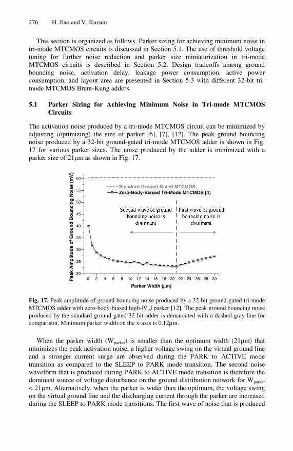
The activation noise produced by a tri-mode MTCMOS circuit can be minimized by adjusting (optimizing) the size of parker [6], [7], [12]. The peak ground bouncing noise produced by a 32-bit ground-gated tri-mode MTCMOS adder is shown in Fig. 17 for various parker sizes. The noise produced by the adder is minimized with a parker size of 21μm as shown in Fig. 17.
0 2 4 6 8 10 12 14 16 18 20 22 24 26 28 3020
25
30
35
40
45
50
55
60
Pea
k A
mp
litu
de
of
Gro
un
d B
ou
nci
ng
No
ise
(mV
)
Parker Width (μm)
Standard Ground-Gated MTCMOS Zero-Body-Biased Tri-Mode MTCMOS [4]
Fig. 17. Peak amplitude of ground bouncing noise produced by a 32-bit ground-gated tri-mode MTCMOS adder with zero-body-biased high-|Vth| parker [12]. The peak ground bouncing noise produced by the standard ground-gated 32-bit adder is demarcated with a dashed gray line for comparison. Minimum parker width on the x-axis is 0.12µm.
When the parker width (Wparker) is smaller than the optimum width (21μm) that minimizes the peak activation noise, a higher voltage swing on the virtual ground line and a stronger current surge are observed during the PARK to ACTIVE mode transition as compared to the SLEEP to PARK mode transition. The second noise waveform that is produced during PARK to ACTIVE mode transition is therefore the dominant source of voltage disturbance on the ground distribution network for Wparker < 21μm. Alternatively, when the parker is wider than the optimum, the voltage swing on the virtual ground line and the discharging current through the parker are increased during the SLEEP to PARK mode transitions. The first wave of noise that is produced
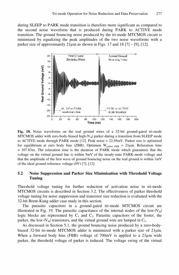
Tri-mode Operation for Noise Reduction and Data Preservation 277
during SLEEP to PARK mode transition is therefore more significant as compared to the second noise waveform that is produced during PARK to ACTIVE mode transition. The ground bouncing noise produced by the tri-mode MTCMOS circuit is minimized by equalizing the peak amplitudes of the two noise waveforms with a parker size of approximately 21µm as shown in Figs. 17 and 18 [7] – [9], [12].
0 20 40 60 80 100 120 140 160 180 200-24
-20
-16
-12
-8
-4
0
4
8
12
16
20
Rea
l Gro
un
d V
olt
age
(mV
)
Time (ns)
Fig. 18. Noise waveforms on the real ground wires of a 32-bit ground-gated tri-mode MTCMOS adder with zero-body-biased high-|Vth| parker during a transition from SLEEP mode to ACTIVE mode through PARK mode [12]. Peak noise = 22.95mV. Parker size is optimized for equilibrium at zero body bias (ZBB). Optimum Wparker_ZBB = 21µm. Relaxation time = 107.83ns. The relaxation time is the duration of PARK mode which guarantees that the voltage on the virtual ground line is within 5mV of the steady-state PARK-mode voltage and that the amplitude of the first wave of ground bouncing noise on the real ground is within 1mV of the ideal ground reference voltage (0V) [7], [12].
5.2 Noise Suppression and Parker Size Minimization with Threshold Voltage Tuning
Threshold voltage tuning for further reduction of activation noise in tri-mode MTCMOS circuits is described in Section 3.2. The effectiveness of parker threshold voltage tuning for noise suppression and transistor size reduction is evaluated with the 32-bit Brent-Kung adder case study in this section.
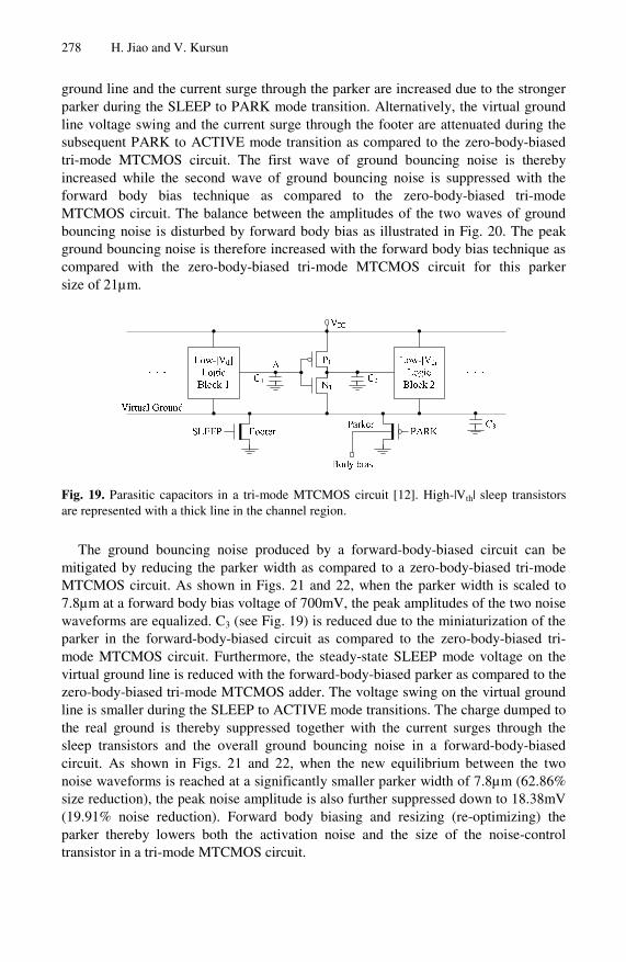
The parasitic capacitors in a ground-gated tri-mode MTCMOS circuit are illustrated in Fig. 19. The parasitic capacitance of the internal nodes of the low-|Vth| logic blocks are represented by C1 and C2. Parasitic capacitors of the footer, the parker, the low-|Vth| transistors, and the virtual ground wire are lumped in C3.
As discussed in Section 5.1, the ground bouncing noise produced by a zero-body-biased 32-bit tri-mode MTCMOS adder is minimized with a parker size of 21μm. When a forward body bias (FBB) voltage of 700mV is applied to a 21µm wide parker, the threshold voltage of parker is reduced. The voltage swing of the virtual
278 H. Jiao and V. Kursun
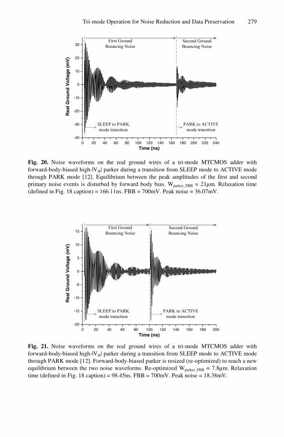
ground line and the current surge through the parker are increased due to the stronger parker during the SLEEP to PARK mode transition. Alternatively, the virtual ground line voltage swing and the current surge through the footer are attenuated during the subsequent PARK to ACTIVE mode transition as compared to the zero-body-biased tri-mode MTCMOS circuit. The first wave of ground bouncing noise is thereby increased while the second wave of ground bouncing noise is suppressed with the forward body bias technique as compared to the zero-body-biased tri-mode MTCMOS circuit. The balance between the amplitudes of the two waves of ground bouncing noise is disturbed by forward body bias as illustrated in Fig. 20. The peak ground bouncing noise is therefore increased with the forward body bias technique as compared with the zero-body-biased tri-mode MTCMOS circuit for this parker size of 21µm.
Fig. 19. Parasitic capacitors in a tri-mode MTCMOS circuit [12]. High-|Vth| sleep transistors are represented with a thick line in the channel region.
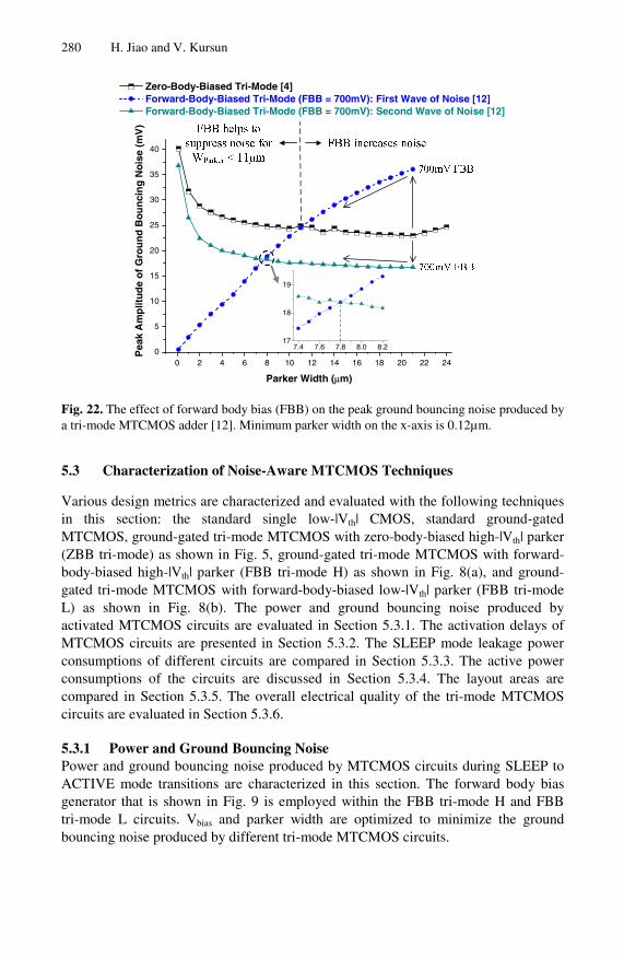
The ground bouncing noise produced by a forward-body-biased circuit can be mitigated by reducing the parker width as compared to a zero-body-biased tri-mode MTCMOS circuit. As shown in Figs. 21 and 22, when the parker width is scaled to 7.8µm at a forward body bias voltage of 700mV, the peak amplitudes of the two noise waveforms are equalized. C3 (see Fig. 19) is reduced due to the miniaturization of the parker in the forward-body-biased circuit as compared to the zero-body-biased tri-mode MTCMOS circuit. Furthermore, the steady-state SLEEP mode voltage on the virtual ground line is reduced with the forward-body-biased parker as compared to the zero-body-biased tri-mode MTCMOS adder. The voltage swing on the virtual ground line is smaller during the SLEEP to ACTIVE mode transitions. The charge dumped to the real ground is thereby suppressed together with the current surges through the sleep transistors and the overall ground bouncing noise in a forward-body-biased circuit. As shown in Figs. 21 and 22, when the new equilibrium between the two noise waveforms is reached at a significantly smaller parker width of 7.8µm (62.86% size reduction), the peak noise amplitude is also further suppressed down to 18.38mV (19.91% noise reduction). Forward body biasing and resizing (re-optimizing) the parker thereby lowers both the activation noise and the size of the noise-control transistor in a tri-mode MTCMOS circuit.
Tri-mode Operation for Noise Reduction and Data Preservation 279
0 20 40 60 80 100 120 140 160 180 200 220 240-40
-30
-20
-10
0
10
20
30
Rea
l Gro
un
d V
olt
age
(mV
)
Time (ns)
SLEEP to PARK mode transition
PARK to ACTIVE mode transition
First Ground Bouncing Noise
Second Ground Bouncing Noise
Fig. 20. Noise waveforms on the real ground wires of a tri-mode MTCMOS adder with forward-body-biased high-|Vth| parker during a transition from SLEEP mode to ACTIVE mode through PARK mode [12]. Equilibrium between the peak amplitudes of the first and second primary noise events is disturbed by forward body bias. Wparker_FBB = 21µm. Relaxation time (defined in Fig. 18 caption) = 166.11ns. FBB = 700mV. Peak noise = 36.07mV.
0 20 40 60 80 100 120 140 160 180 200-20
-15
-10
-5
0
5
10
15
Rea
l Gro
un
d V
olt
age
(mV
)
Time (ns)
SLEEP to PARK mode transition
PARK to ACTIVE mode transition
First Ground Bouncing Noise
Second Ground Bouncing Noise
Fig. 21. Noise waveforms on the real ground wires of a tri-mode MTCMOS adder with forward-body-biased high-|Vth| parker during a transition from SLEEP mode to ACTIVE mode through PARK mode [12]. Forward-body-biased parker is resized (re-optimized) to reach a new equilibrium between the two noise waveforms. Re-optimized Wparker_FBB = 7.8µm. Relaxation time (defined in Fig. 18 caption) = 98.45ns. FBB = 700mV. Peak noise = 18.38mV.
280 H. Jiao and V. Kursun
7.4 7.6 7.8 8.0 8.217
18
19
0 2 4 6 8 10 12 14 16 18 20 22 240
5
10
15
20
25
30
35
40P
eak
Am
plit
ud
e o
f G
rou
nd
Bo
un
cin
g N
ois
e (m
V)
Parker Width (μm)
Zero-Body-Biased Tri-Mode [4] Forward-Body-Biased Tri-Mode (FBB = 700mV): First Wave of Noise [12] Forward-Body-Biased Tri-Mode (FBB = 700mV): Second Wave of Noise [12]
Fig. 22. The effect of forward body bias (FBB) on the peak ground bouncing noise produced by a tri-mode MTCMOS adder [12]. Minimum parker width on the x-axis is 0.12µm.
5.3 Characterization of Noise-Aware MTCMOS Techniques
Various design metrics are characterized and evaluated with the following techniques in this section: the standard single low-|Vth| CMOS, standard ground-gated MTCMOS, ground-gated tri-mode MTCMOS with zero-body-biased high-|Vth| parker (ZBB tri-mode) as shown in Fig. 5, ground-gated tri-mode MTCMOS with forward-body-biased high-|Vth| parker (FBB tri-mode H) as shown in Fig. 8(a), and ground-gated tri-mode MTCMOS with forward-body-biased low-|Vth| parker (FBB tri-mode L) as shown in Fig. 8(b). The power and ground bouncing noise produced by activated MTCMOS circuits are evaluated in Section 5.3.1. The activation delays of MTCMOS circuits are presented in Section 5.3.2. The SLEEP mode leakage power consumptions of different circuits are compared in Section 5.3.3. The active power consumptions of the circuits are discussed in Section 5.3.4. The layout areas are compared in Section 5.3.5. The overall electrical quality of the tri-mode MTCMOS circuits are evaluated in Section 5.3.6.
5.3.1 Power and Ground Bouncing Noise Power and ground bouncing noise produced by MTCMOS circuits during SLEEP to ACTIVE mode transitions are characterized in this section. The forward body bias generator that is shown in Fig. 9 is employed within the FBB tri-mode H and FBB tri-mode L circuits. Vbias and parker width are optimized to minimize the ground bouncing noise produced by different tri-mode MTCMOS circuits.
Tri-mode Operation for Noise Reduction and Data Preservation 281
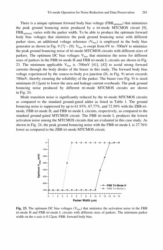
There is a unique optimum forward body bias voltage (FBBoptimum) that minimizes the peak ground bouncing noise produced by a tri-mode MTCMOS circuit [9]. FBBoptimum varies with the parker width. To be able to produce the optimum forward body bias voltages that minimize the peak ground bouncing noise with different parker sizes, an additional voltage reference (Vbias) is employed in the body bias generator as shown in Fig. 9 [7] – [9]. Vbias is swept from 0V to -700mV to minimize the peak ground bouncing noise of tri-mode MTCMOS circuits with different sizes of parkers. The optimum DC bias voltages Vbias that minimize the noise for different sizes of parkers in the FBB tri-mode H and FBB tri-mode L circuits are shown in Fig. 23. The minimum applicable Vbias is -700mV [41], [42] to avoid strong forward currents through the body diodes of the biaser in this study. The forward body bias voltage experienced by the source-to-body p-n junction (D1 in Fig. 9) never exceeds 700mV, thereby ensuring the reliability of the parker. The biaser (see Fig. 9) is sized minimum (0.12µm) to lower the area and leakage current overheads. The peak ground bouncing noise produced by different tri-mode MTCMOS circuits are shown in Fig. 24.
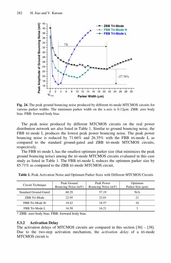
Mode transition noise is significantly reduced by the tri-mode MTCMOS circuits as compared to the standard ground-gated adder as listed in Table 1. The ground bouncing noise is suppressed by up to 61.93%, 67.77%, and 72.50% with the ZBB tri-mode, FBB tri-mode H, and FBB tri-mode L circuits, respectively, as compared to the standard ground-gated MTCMOS circuit. The FBB tri-mode L produces the lowest activation noise among the MTCMOS circuits that are evaluated in this case study. As shown in Fig. 24, the peak ground bouncing noise with the FBB tri-mode L is 27.76% lower as compared to the ZBB tri-mode MTCMOS circuit.
0 1 2 3 4 5 6 7 8 9 10 11 12 13 14 15
-700
-600
-500
-400
-300
-200
-100
0
FBB Tri-Mode H FBB Tri-Mode L
Op
tim
um
Vb
ias
(mV
)
Parker Width (μm)
Fig. 23. The optimum DC bias voltages (Vbias) that minimize the activation noise in the FBB tri-mode H and FBB tri-mode L circuits with different sizes of parkers. The minimum parker width on the x-axis is 0.12µm. FBB: forward body bias.
282 H. Jiao and V. Kursun
7X
–27.76%
Wmin
0 2 4 6 8 10 12 14 16 18 20 22 24 26 28 30
16
18
20
22
24
26
28
30
32
34
36
38
40
42
Pea
k A
mp
litu
de
of
Gro
un
d B
ou
nci
ng
No
ise
(mV
)
Parker Width (μm)
ZBB Tri-Mode FBB Tri-Mode H FBB Tri-Mode L
Fig. 24. The peak ground bouncing noise produced by different tri-mode MTCMOS circuits for various parker widths. The minimum parker width on the x-axis is 0.12µm. ZBB: zero body bias. FBB: forward body bias.
The peak noise produced by different MTCMOS circuits on the real power distribution network are also listed in Table 1. Similar to ground bouncing noise, the FBB tri-mode L produces the lowest peak power bouncing noise. The peak power bouncing noise is reduced by 71.66% and 26.35% with the FBB tri-mode L as compared to the standard ground-gated and ZBB tri-mode MTCMOS circuits, respectively.
The FBB tri-mode L has the smallest optimum parker size (that minimizes the peak ground bouncing noise) among the tri-mode MTCMOS circuits evaluated in this case study as listed in Table 1. The FBB tri-mode L reduces the optimum parker size by 85.71% as compared to the ZBB tri-mode MTCMOS circuit.
Table 1. Peak Activation Noise and Optimum Parker Sizes with Different MTCMOS Circuits
Circuit Technique Peak Ground
Bouncing Noise (mV) Peak Power
Bouncing Noise (mV) Optimum
Parker Size (µm)
Standard Ground-Gated 60.29 57.19 N/A
ZBB Tri-Mode 22.95 22.01 21
FBB Tri-Mode H 19.43 18.57 10
FBB Tri-Mode L 16.58 16.21 3
* ZBB: zero body bias. FBB: forward body bias.
5.3.2 Activation Delay The activation delays of MTCMOS circuits are compared in this section [36] – [38]. Due to the two-step activation mechanism, the activation delay of a tri-mode MTCMOS circuit is

Tri-mode Operation for Noise Reduction and Data Preservation 283
Activation Delay Relaxation Time Wake Up Delay= + , (1)
where wake up delay is the time interval from the 50% rising edge of the SLEEP signal until the virtual ground voltage stabilizes below 10mV. Relaxation time is defined in Fig. 18 caption. For the standard ground-gated MTCMOS circuits that directly transition from SLEEP mode to ACTIVE mode, there is no relaxation time and the activation delay is equal to the wake up delay.
Table 2. Activation Delays (ns) of Different MTCMOS Circuits
Circuit Technique Relaxation Time Wake Up Delay Activation Delay
Standard Ground-Gated N/A 15.29 15.29
ZBB Tri-Mode 107.82 12.16 119.98
FBB Tri-Mode H 101.12 9.36 110.48
FBB Tri-Mode L 75.95 4.84 80.79
* ZBB: zero body bias. FBB: forward body bias.
Due to the two-step activation mechanism, all the tri-mode MTCMOS circuits significantly increase the SLEEP to ACTIVE mode transition delay as compared to the standard ground-gated MTCMOS circuit, as listed in Table 2. Among the noise-aware MTCMOS circuit techniques, the ZBB tri-mode MTCMOS circuit has the longest activation delay. Alternatively, FBB tri-mode L provides the quickest activation primarily due to the lowest steady-state PARK mode voltage on the virtual ground line, the lowest threshold voltage of the forward-body-biased parker, and the fastest discharging of C3 (see Fig. 19) among the tri-mode MTCMOS circuits that are evaluated in this case study. The FBB tri-mode L reduces the activation delay by 32.66% as compared to the ZBB tri-mode MTCMOS circuit.
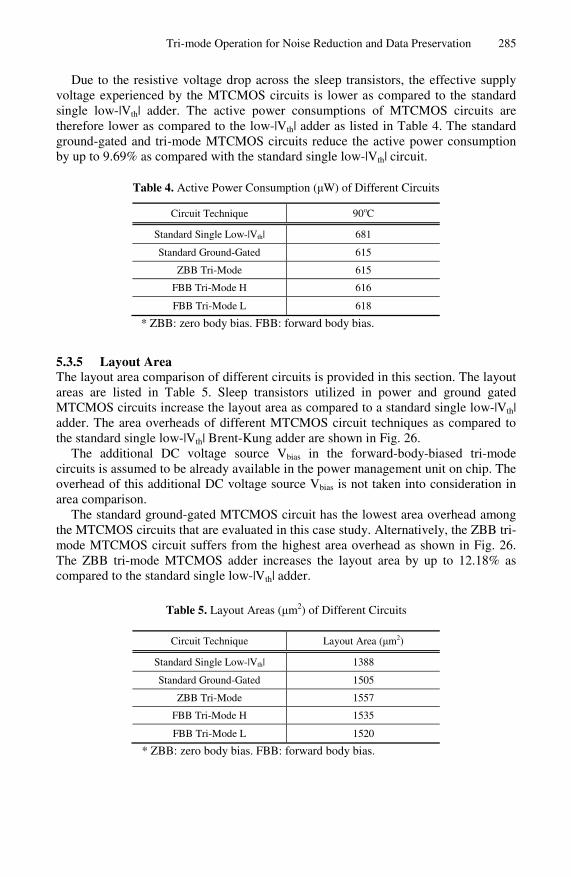
5.3.3 Leakage Power Consumption The worst case leakage power consumptions of the standard single low-|Vth|, standard ground-gated MTCMOS, ZBB tri-mode, FBB tri-mode H, and FBB tri-mode L circuits in the SLEEP mode are evaluated in this section. The leakage power consumed by the circuits at 25˚C and 90˚C are listed in Table 3. The percent leakage power savings provided by different MTCMOS circuit techniques as compared to the standard single low-|Vth| circuit are shown in Fig. 25. The input vectors applied to the 32-bit adders are “0” [6].
The standard ground-gated MTCMOS circuit consumes the lowest leakage power among the circuits that are evaluated in this case study. As listed in Table 3, the leakage power consumption is reduced by up to 99.75%, 41.01%, 92.44%, and 95.05% by the standard ground-gated MTCMOS circuit as compared to the standard single low-|Vth|, ZBB tri-mode, FBB tri-mode H, and FBB tri-mode L circuits, respectively. Since the threshold voltage of the parker is the lowest and the forward biased p-n junction currents through the parker and biaser are the highest, the FBB tri-mode L consumes the highest leakage power in the SLEEP mode among the
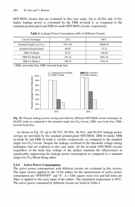
284 H. Jiao and V. Kursun
MTCMOS circuits that are evaluated in this case study. Up to 20.20x and 11.92x higher leakage power is consumed by the FBB tri-mode L as compared to the standard ground-gated and ZBB tri-mode MTCMOS circuits, respectively.
Table 3. Leakage Power Consumption (nW) of Different Circuits
Circuit Technique 25˚C 90˚C
Standard Single Low-|Vth| 6971.40 30896.94
Standard Ground-Gated 60.92 75.74
ZBB Tri-Mode 65.41 128.40
FBB Tri-Mode H 341.12 1001.24
FBB Tri-Mode L 390.76 1530.14
* ZBB: zero body bias. FBB: forward body bias.
FBB Tri-Mode H FBB Tri-Mode L100%
99%
98%
97%
96%
95%
94%
90oC93%P
erce
nt L
eaka
ge P
ower
Red
uctio
n
Standard Ground-Gated ZBB Tri-Mode
25oC
Fig. 25. Percent leakage power savings provided by different MTCMOS circuit techniques in SLEEP mode as compared to the standard single low-|Vth| circuit. ZBB: zero body bias. FBB: forward body bias.
As shown in Fig. 25, up to 99.75%, 99.58%, 96.76%, and 95.05% leakage power savings are provided by the standard ground-gated MTCMOS, ZBB tri-mode, FBB tri-mode H, and FBB tri-mode L circuits, respectively, as compared to the standard single low-|Vth| circuit. Despite the leakage overhead of the threshold voltage tuning techniques that are explored in this case study, all the tri-mode MTCMOS circuits (regardless of the body bias voltage of the parker) maintain the effectiveness in significantly suppressing the leakage power consumption as compared to a standard single low-|Vth| Brent-Kung adder.
5.3.4 Active Power Consumption The active power consumptions with different circuits are evaluated in this section. The input vectors applied to the 32-bit adders for the measurement of active power consumption are “FFFFFFFF” and “0”. A 1 GHz square wave (rise and fall times are 50ps) is applied to the carry input of the adders. The simulation temperature is 90˚C. The active power consumed by different circuits are listed in Table 4.
Tri-mode Operation for Noise Reduction and Data Preservation 285
Due to the resistive voltage drop across the sleep transistors, the effective supply voltage experienced by the MTCMOS circuits is lower as compared to the standard single low-|Vth| adder. The active power consumptions of MTCMOS circuits are therefore lower as compared to the low-|Vth| adder as listed in Table 4. The standard ground-gated and tri-mode MTCMOS circuits reduce the active power consumption by up to 9.69% as compared with the standard single low-|Vth| circuit.
Table 4. Active Power Consumption (μW) of Different Circuits
Circuit Technique 90oC
Standard Single Low-|Vth| 681
Standard Ground-Gated 615
ZBB Tri-Mode 615
FBB Tri-Mode H 616
FBB Tri-Mode L 618
* ZBB: zero body bias. FBB: forward body bias.
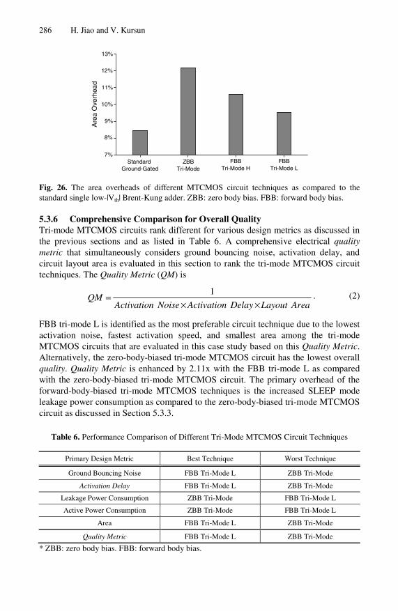
5.3.5 Layout Area The layout area comparison of different circuits is provided in this section. The layout areas are listed in Table 5. Sleep transistors utilized in power and ground gated MTCMOS circuits increase the layout area as compared to a standard single low-|Vth| adder. The area overheads of different MTCMOS circuit techniques as compared to the standard single low-|Vth| Brent-Kung adder are shown in Fig. 26.
The additional DC voltage source Vbias in the forward-body-biased tri-mode circuits is assumed to be already available in the power management unit on chip. The overhead of this additional DC voltage source Vbias is not taken into consideration in area comparison.
The standard ground-gated MTCMOS circuit has the lowest area overhead among the MTCMOS circuits that are evaluated in this case study. Alternatively, the ZBB tri-mode MTCMOS circuit suffers from the highest area overhead as shown in Fig. 26. The ZBB tri-mode MTCMOS adder increases the layout area by up to 12.18% as compared to the standard single low-|Vth| adder.
Table 5. Layout Areas (μm2) of Different Circuits
Circuit Technique Layout Area (μm2)
Standard Single Low-|Vth| 1388
Standard Ground-Gated 1505
ZBB Tri-Mode 1557
FBB Tri-Mode H 1535
FBB Tri-Mode L 1520
* ZBB: zero body bias. FBB: forward body bias.
286 H. Jiao and V. Kursun
13%
12%
11%
10%
9%
8%
7%FBB
Tri-Mode HZBB
Tri-ModeStandard
Ground-Gated
Are
a O
verh
ead
FBBTri-Mode L
Fig. 26. The area overheads of different MTCMOS circuit techniques as compared to the standard single low-|Vth| Brent-Kung adder. ZBB: zero body bias. FBB: forward body bias.
5.3.6 Comprehensive Comparison for Overall Quality Tri-mode MTCMOS circuits rank different for various design metrics as discussed in the previous sections and as listed in Table 6. A comprehensive electrical quality metric that simultaneously considers ground bouncing noise, activation delay, and circuit layout area is evaluated in this section to rank the tri-mode MTCMOS circuit techniques. The Quality Metric (QM) is
1QM
Activation Noise Activation Delay Layout Area=
× ×. (2)
FBB tri-mode L is identified as the most preferable circuit technique due to the lowest activation noise, fastest activation speed, and smallest area among the tri-mode MTCMOS circuits that are evaluated in this case study based on this Quality Metric. Alternatively, the zero-body-biased tri-mode MTCMOS circuit has the lowest overall quality. Quality Metric is enhanced by 2.11x with the FBB tri-mode L as compared with the zero-body-biased tri-mode MTCMOS circuit. The primary overhead of the forward-body-biased tri-mode MTCMOS techniques is the increased SLEEP mode leakage power consumption as compared to the zero-body-biased tri-mode MTCMOS circuit as discussed in Section 5.3.3.
Table 6. Performance Comparison of Different Tri-Mode MTCMOS Circuit Techniques
Primary Design Metric Best Technique Worst Technique
Ground Bouncing Noise FBB Tri-Mode L ZBB Tri-Mode
Activation Delay FBB Tri-Mode L ZBB Tri-Mode
Leakage Power Consumption ZBB Tri-Mode FBB Tri-Mode L
Active Power Consumption ZBB Tri-Mode FBB Tri-Mode L
Area FBB Tri-Mode L ZBB Tri-Mode
Quality Metric FBB Tri-Mode L ZBB Tri-Mode
* ZBB: zero body bias. FBB: forward body bias.

Tri-mode Operation for Noise Reduction and Data Preservation 287
6 Chapter Summary
Power and ground bouncing noise that are produced during SLEEP to ACTIVE mode transitions are the most important reliability issues in MTCMOS circuits. Activation noise in MTCMOS circuits is examined in this chapter. Factors affecting the amplitude of mode transition noise are identified. A specialized MTCMOS technique with three modes of operation is described to suppress the activation noise in power and ground gated integrated circuits. A two-step wake-up mechanism with an additional intermediate PARK mode is employed with the tri-mode MTCMOS circuits. The activation noise is reduced by lowering the voltage swing on the virtual power and ground lines and limiting the current surges through the sleep transistors during the transitions from SLEEP mode to ACTIVE mode through PARK mode in a tri-mode MTCMOS circuit.
Different tri-mode MTCMOS circuit design options are explored to minimize the mode transition noise with smaller sleep transistors and shorter activation delay. The principal mechanisms of activation noise suppression and parker size reduction with threshold voltage tuned tri-mode MTCMOS circuits are explained. Design guidelines are provided for appropriate sizing of noise-control transistor and selection of body bias voltage to fully utilize the benefits of tri-mode MTCMOS circuit technique. Alternative applications of tri-mode MTCMOS for data preservation and leakage power reduction in idle memory elements are also described in this chapter.
References
1. Kursun, V., Friedman, E.G.: Multi-Voltage CMOS Circuit Design. John Wiley & Sons Ltd. (2006) ISBN # 0-470-01023-1
2. Kurd, N.A., Bhamidipati, S., Mozak, C., Miller, J.L., Mosalikanti, P., Wilson, T.M., El-Husseini, A.M., Neidengard, M., Aly, R.E., Nemani, M., Chowdhury, M., Kumar, R.: A family of 32nm IA processors. IEEE Journal of Solid-State Circuits 46(1), 119–130 (2011)
3. Mutoh, S., Douseki, T., Matsuya, Y., Aoki, T., Shigematsu, S., Yamada, J.: 1-V power supply high-speed digital circuit technology. IEEE Journal of Solid-State Circuits 30(8), 847–854 (1995)
4. Kim, S., Kosonocky, S.V., Knebel, D.R., Stawiasz, K., Papaefthymiou, M.C.: A multi-mode power gating structure for low-voltage deep-submicron CMOS ICs. IEEE Transactions on Circuits and Systems II 54(7), 586–590 (2007)
5. Kim, S., Kosonocky, S.V., Knebel, D.R.: Understanding and minimizing ground bounce during mode transition of power gating structures. In: Proceedings of the IEEE/ACM International Symposium on Low Power Electronics and Design, pp. 22–25 (August 2003)
6. Jiao, H., Kursun, V.: Ground-bouncing-noise-aware combinational MTCMOS circuits. IEEE Transactions on Circuits and Systems I 57(8), 2053–2065 (2010)
7. Jiao, H., Kursun, V.: Threshold voltage tuning for faster activation with lower noise in tri-mode MTCMOS circuits. IEEE Transactions on Very Large Scale Integration (VLSI) Systems 20(4) (2012)
8. Jiao, H., Kursun, V.: Dynamic forward body bias enhanced tri-mode MTCMOS. In: Proceedings of the IEEE Asia Symposium on Quality Electronic Design, pp. 33–37 (August 2010)
288 H. Jiao and V. Kursun
9. Jiao, H., Kursun, V.: Sleep transistor forward body bias: an extra knob to lower ground bouncing noise in MTCMOS circuits. In: Proceedings of the IEEE International SoC Design Conference, pp. 216–219 (November 2009)
10. Jiao, H., Kursun, V.: Reactivation noise suppression with threshold voltage tuning in sequential MTCMOS circuits. In: Proceedings of the IEEE International Conference on VLSI and System-on-Chip (VLSI-SoC), pp. 347–351 (September 2010)
11. Jiao, H., Kursun, V.: Noise-aware data preserving sequential MTCMOS circuits with dynamic forward body bias. Journal of Circuits, Systems, and Computers 20(1), 125–145 (2011)
12. Jiao, H., Kursun, V.: How forward body bias helps to reduce ground bouncing noise and silicon area in MTCMOS circuits: divulging the basic mechanism. In: Proceedings of the IEEE International SoC Design Conference, pp. 9–12 (November 2010)
13. Jiao, H., Kursun, V.: Ground bouncing noise suppression techniques for data preserving sequential MTCMOS circuits. IEEE Transactions on Very Large Scale Integration (VLSI) Systems 19(5), 763–773 (2011)
14. Kim, S., Choi, C.J., Jeong, D.K., Kosonocky, S.V., Park, S.B.: Reducing ground-bounce noise and stabilizing the data-retention voltage of power-gating structures. IEEE Transactions on Electron Devices 55(1), 197–205 (2008)
15. Jiang, H., Sadowska, M.M.: Power gating scheduling for power/ground noise reduction. In: Proceedings of the IEEE/ACM International Design Automation Conference, pp. 980–985 (June 2008)
16. Kawasaki, K., Shiota, T., Nakayama, K., Inoue, A.: A sub- µs wake-up time power gating technique with bypass power line for rush current support. IEEE Journal of Solid-State Circuits 44(4), 1178–1183 (2009)
17. Min, K.S., Kawaguchi, H., Sakurai, T.: Zigzag super cut-off CMOS (ZSCCMOS) block activation with self-adaptive voltage level controller: an alternative to clock-gating scheme in leakage dominant era. In: Proceedings of the IEEE International Solid-State Circuits Conference, pp. 400–401 (February 2003)
18. Pakbaznia, E., Fallah, F., Pedram, M.: Charge recycling in power-gated CMOS circuits. IEEE Transactions on Computer-Aided Design of Integrated Circuits and Systems 27(10), 1798–1811 (2008)
19. Liu, Z., Kursun, V.: Charge recycling between virtual power and ground lines for low energy MTCMOS. In: Proceedings of the IEEE/ACM International Symposium on Quality Electronic Design, pp. 239–244 (March 2007)
20. Liu, Z., Kursun, V.: Low energy MTCMOS with sleep transistor charge recycling. In: Proceedings of the IEEE International Midwest Symposium on Circuits and Systems, pp. 891–894 (August 2007)
21. Bhavnagarwala, A.J., Kosonocky, S.V., Immediato, M., Knebel, D., Haen, A.M.: A pico-joule class, 1GHz, 32KByte x 64b DSP SRAM with self reverse bias. In: Proceedings of the IEEE Symposium on VLSl Circuits, pp. 253–254 (June 2003)
22. Zhang, K., Bhattacharya, U., Chen, Z., Hamzaoglu, F., Murray, D., Vallepalli, N., Wang, Y., Zheng, B., Bohr, M.: SRAM design on 65-nm CMOS technology with dynamic sleep transistor for leakage reduction. IEEE Journal of Solid-State Circuits 40(4), 895–901 (2005)
23. Riedlinger, R., Bhatia, R., Biro, L., Bowhill, B., Fetzer, E., Gronowski, P., Grutkowski, T.: A 32nm 3.1 billion transistor 12-wide-issue Itanium processor for mission-critical servers. In: Proceedings of the IEEE International Solid-State Circuits Conference, pp. 84–85 (February 2011)
Tri-mode Operation for Noise Reduction and Data Preservation 289
24. Kanno, Y., Mizuno, H., Yasu, Y., Hirose, K., Shimazaki, Y., Hoshi, T., Miyairi, Y., Ishii, T., Yamada, T., Irita, T., Hattori, T., Yanagisawa, K., Irie, N.: Hierarchical power distribution with power tree in dozens of power domains for 90-nm low-power multi-CPU SoCs. IEEE Journal of Solid-State Circuits 42(1), 74–83 (2007)
25. Shin, J., Huang, D., Petrick, B., Hwang, C., Tam, K., Smith, A., Pham, H., Li, H., Johnson, T., Schumacher, F., Leon, A., Strong, A.: A 40 nm 16-core 128-thread SPARC SoC processor. IEEE Journal of Solid-State Circuits 46(1), 131–144 (2011)
26. Wendel, D., Kalla, R., Warnock, J., Cargnoni, R., Chu, S., Clabes, J., Dreps, D., Hrusecky, D., Friedrich, J., Islam, S., Kahle, J., Leenstra, J., Mittal, G., Paredes, J., Pille, J., Restle, P., Sinharoy, B., Smith, G., Starke, W., Taylor, S., Norstrand, A.J.V., Weitzel, S., Williams, P., Zyuban, V.: POWER7, a highly parallel, scalable multi-core high end server processor. IEEE Journal of Solid-State Circuits 46(1), 145–161 (2011)
27. Calhoun, B.H., Honoré, F.A., Chandrakasan, A.P.: A leakage reduction methodology for distributed MTCMOS. IEEE Journal of Solid-State Circuits 39(5), 818–826 (2004)
28. Kao, J., Chandrakasan, A., Antoniadis, D.: Transistor sizing issues and tool for multi-threshold CMOS technology. In: Proceedings of the IEEE /ACM International Design Automation Conference, pp. 409–414 (June 1997)
29. Shigematsu, S., Mutoh, S., Matsuya, Y., Tanabe, Y., Yamada, J.: A 1-V high-speed MTCMOS circuit scheme for power-down application circuits. IEEE Journal of Solid-State Circuits 32(6), 861–869 (1997)
30. Stan, M.R., Barcella, M.: MTCMOS with outer feedback (MTOF) flip-flops. In: Proceedings of the IEEE International Symposium on Circuits and Systems, pp. 429–432 (May 2003)
31. Liu, Z., Kursun, V.: New MTCMOS flip-flops with simple control circuitry and low leakage data retention capability. In: Proceedings of the IEEE International Conference on Electronics, Circuits, and Systems, pp. 1276–1279 (December 2007)
32. Jiao, H., Kursun, V.: Low-leakage and compact registers with easy-sleep mode. Journal of Low-Power Electronics 6(2), 263–279 (2010)
33. Jiao, H., Kursun, V.: Power gated SRAM circuits with data retention capability and high immunity to noise: a comparison for reliability in low leakage sleep mode. In: Proceedings of the IEEE International SoC Design Conference, pp. 5–8 (November 2010)
34. Jiao, H., Kursun, V.: Asymmetrical ground gating for low leakage and data robust sleep mode in memory banks. In: Proceedings of the IEEE International Symposium on VLSI Design Automation and Test, pp. 205–208 (April 2011)
35. Seomun, J., Shin, Y.: Design and optimization of power-gated circuits with autonomous data retention. IEEE Transactions on Very Large Scale Integration (VLSI) Systems 19(2), 227–236 (2011)
36. Hu, Z., Buyuktosunoglu, A., Srinivasan, V., Zyuban, V., Jacobson, H., Bose, P.: Microarchitectural techniques for power gating of execution units. In: Proceedings of the IEEE/ACM International Symposium on Low Power Electronics and Design, pp. 32–37 (August 2004)
37. Singh, H., Agarwal, K., Sylvester, D., Nowka, K.J.: Enhanced leakage reduction techniques using intermediate strength power gating. IEEE Transactions on Very Large Scale Integration (VLSI) Systems 15(11), 1215–1224 (2007)
38. Dropsho, S., Kursun, V., Albonesi, D.H., Dwarkadas, S., Friedman, E.G.: Managing static leakage energy in microprocessor functional units. In: Proceedings of the IEEE/ACM International Symposium on Microarchitecture, pp. 321–332 (November 2002)
39. Kursun, V., Friedman, E.G.: Domino logic with dynamic body biased keeper. In: Proceedings of the European Solid-State Circuits Conference, pp. 675–678 (September 2002)
290 H. Jiao and V. Kursun
40. Kursun, V., Friedman, E.G.: Forward body biased keeper for enhanced noise immunity in domino logic circuits. In: Proceedings of the IEEE International Symposium on Circuits and Systems, vol. 2, pp. 917–920 (May 2004)
41. Narendra, S., Tschanz, J., Hofsheier, J., Bloechel, B., Vangal, S., Hoskote, Y., Tang, S., Somasekhar, D., Keshavarzi, A., Erraguntla, V., Dermer, G., Borkar, N., Borkar, S., De, V.: Ultra-low voltage circuits and processor in 180nm to 90nm technologies with a swapped-body biasing technique. In: Proceedings of the IEEE International Solid-State Circuits Conference, pp. 156–518 (February 2004)
42. Narendra, S., Keshavarzi, A., Bloechel, B.A., Borkar, S., De, V.: Forward body bias for microprocessors in 130-nm technology generation and beyond. IEEE Journal of Solid-State Circuits 38(5), 696–701 (2003)
43. Liu, Z., Kursun, V.: Characterization of a novel nine transistor SRAM cell. IEEE Transactions on Very Large Scale Integration (VLSI) Systems 16(4), 488–492 (2008)
44. Liu, Z., Kursun, V.: High read stability and low leakage cache memory cell. In: Proceedings of the IEEE International Symposium on Circuits and Systems, pp. 2774–2777 (May 2007)
45. Tawfik, S.A., Kursun, V.: Low power and robust 7T dual-Vt SRAM circuit. In: Proceedings of the IEEE International Symposium on Circuits and Systems, pp. 1452–1455 (May 2008)
46. Zhu, H., Kursun, V.: Application-specific selection of 6T SRAM cells offering superior performance and quality with a triple-threshold-voltage CMOS technology. In: Proceedings of the IEEE Asia Symposium on Quality Electronic Design (July 2011)
47. Kursun, V., Tawfik, S.A., Liu, Z.: Leakage-aware design of nanometer SoC. In: Proceedings of the IEEE International Symposium on Circuits and Systems, pp. 3231–3234 (May 2007)
48. Black, B., Annavaram, M., Brekelbaum, N., DeVale, J., Jiang, L., Loh, G.H., McCauley, D., Morrow, P., Nelson, D.W., Pantuso, D., Reed, P., Rupley, J., Shankar, S., Shen, J., Webb, C.: Die stacking (3D) microarchitecture. In: Proceedings of the IEEE/ACM International Symposium on Microarchitecture, pp. 469–479 (December 2006)
49. Heydari, P., Pedram, M.: Ground bounce in digital VLSI circuits. IEEE Transactions on Very Large Scale Integration (VLSI) Systems 11(2), 180–185 (2003)
50. UMC 80 Nanometer CMOS Technology, http://www.umc.com/english/process/g.asp