impact of random telegraph noise on cmos logic delay ... · impact of random telegraph noise on...
TRANSCRIPT

Impact of Random Telegraph Noise on CMOSLogic Delay Uncertainty
Takashi MatsumotoDepartment of Communications
and Computer EngineeringKyoto University, Kyoto, Japan
Email: [email protected]
Kazutoshi KobayashiDepartment of Electronics
Kyoto Institute of Technology, Kyoto, Japan
Hidetoshi OnoderaDepartment of Communications
and Computer EngineeringKyoto University, Kyoto, Japan
Abstract—Statistical nature of RTN-induced delay fluctuationis described by measuring 2,520 ROs fabricated in a commercial40 nm CMOS technology. Small number of samples have a largeRTN-induced delay fluctuation. RTN-induced delay fluctuationbecomes as much as 10.4% of nominal oscillation frequencyunder low supply voltage (0.65V). By slightly increasing the tran-sistor size, more than 50% reduction of frequency uncertaintycan be achieved under 0.75V operation. Circuit designers canchange various parameters such as operating voltage, transistorsize, logic stage number, logic gate type, and substrate bias.The impact of the parameters that can be changed by circuitdesigners is clarified in view of RTN-induced CMOS logic delayuncertainty.
I. INTRODUCTION
Designing reliable systems has become more difficult inrecent years[1]-[3]. In addition to conventional problems suchas transistor leakage, the degradation and variation of transis-tor performance have a severe impact on the dependabilityof VLSI systems. Random Telegraph Noise (RTN)[4] andNegative Bias Temperature Instability (NBTI)[5][6] are majorreliability concerns for CMOS circuits. When transistors de-grade owing to NBTI, the propagation delay of combinationallogic increases. The correct operation of a register may notbe guaranteed. Furthermore, the timing of registers that isgenerated by a clock tree may be skewed. As a result, owingto NBTI degradation, the circuit does not operate correctlyor does not reach the lower limit of LSI performance. Aremarkable phenomenon regarding NBTI is that the degradedperformance of a pMOS transistor recovers when the biastemperature stress applied to the gate oxide is removed orrelaxed[7]. RTN has attracted much attention as a temporaltransistor performance fluctuation. RTN occurs in both pMOSand nMOS. RTN is an intrinsically random phenomenon. RTNalready has a serious impact on CMOS image sensors[8],flash memories[9], and SRAMs[10]-[12]. Recently we haveshown that RTN also induces performance fluctuation to logiccircuits[13]. In this paper, we investigated the impact of RTNon CMOS logic delay uncertainty based on the measurementdata. Circuit designers can change various parameters suchas operating voltage, transistor size, logic stage number, logicgate type, and substrate bias. However, the impact of suchparameters on RTN is not well understood at the circuitlevel[14]. The main contribution of this paper is clarifyingthis impact based on the measurement data.
C L KR e g i s t e r( S e q u e n t i a l L o g i c ) C L KR e g i s t e r( S e q u e n t i a l L o g i c )L o g i c P a t h ( C o m b i n a t i o n a l L o g i c )S y n c h r o n o u s C i r c u i tFig. 1. Typical synchronous circuit structure.
C o m b i n a t i o n a l c i r c u i t d e l a y E m u l a t e d b y R O o s c i l l a t i o n f r e q u e n c y
P o w e r S u p p l y V D D R O , V D D D F F c a n b e s e p a r a t e l y c o n t r o l l e d .S u b s t r a t e B i a s ( p # t y p e , n # t y p e ) c a n b e s e p a r a t e l y c o n t r o l l e d .
S e q u e n t i a l c i r c u i t o p e r a t i o n E m u l a t e d b y D F F t o g g l e d b y t h e R OC L KD F F u n d e r T e s t
E N R O u n d e r T e s tD Q D i v i d e rT o C o u n t e r
V D D R OV D D D F F
Fig. 2. Simplest test structure that can emulate the synchronous circuitoperation.
II. TEST STRUCTURE FOR RTN EVALUATION
Figure 1 shows a typical synchronous circuit structure wherea logic path exists between two registers. Figure 2 shows thesimplest test structure that can emulate the synchronous circuitoperation of Fig. 1. Combinational circuit delay is emulatedby ring oscillator (RO) oscillation frequency. Sequential circuitoperation is emulated by D flip-flop (DFF) toggled by theRO output. The power supply for RO (VDDRO) and DFF(VDDDFF) can be independently controlled. We can also con-trol the substrate bias for pMOS and nMOS. Figure 3 showsthe whole test structure for the RTN measurement. RTN-
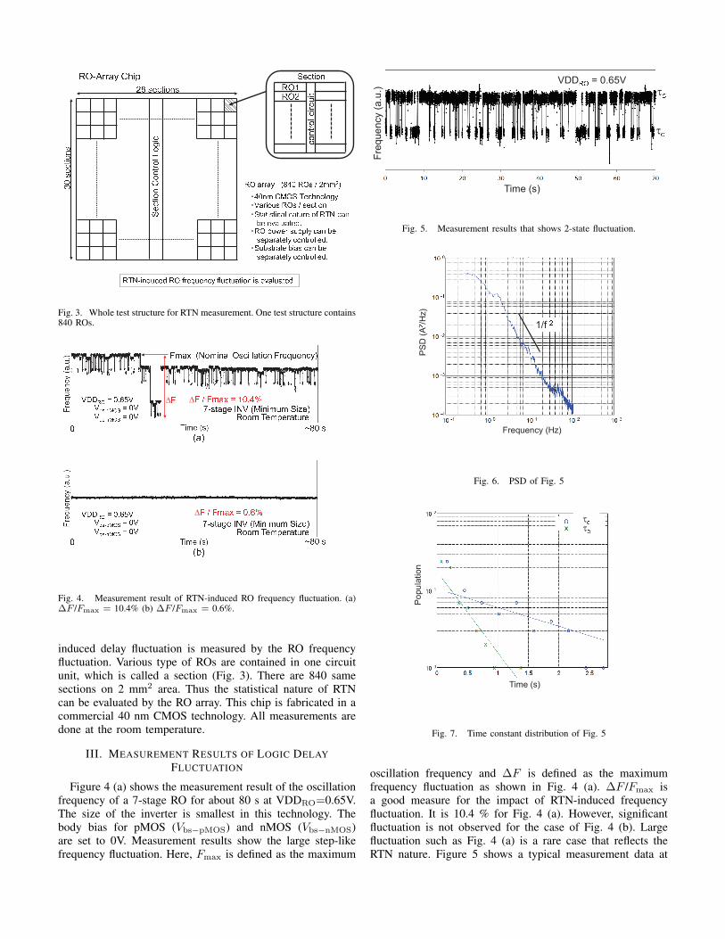
R O a r r a y ( 8 4 0 R O s / 2 m m 2 )S t a t i s t i c a l n a t u r e o f R T N c a nb e e v a l u a t e d .R O p o w e r s u p p l y c a n b es e p a r a t e l y c o n t r o l l e d .R T N ! i n d u c e d R O f r e q u e n c y f l u c t u a t i o n i s e v a l u a t e d .4 0 n m C M O S T e c h n o l o g yV a r i o u s R O s / s e c t i o nS u b s t r a t e b i a s c a n b es e p a r a t e l y c o n t r o l l e d .
cont rol ci rcuitR O 1R O 22 8 s e c t i o n s30 secti ons
R O H A r r a y C h i p
S ecti onC ont rolL ogi cS e c t i o n
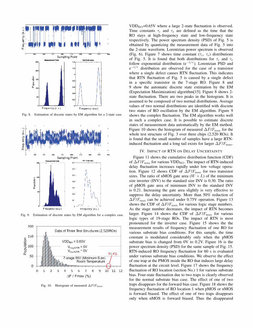
Fig. 3. Whole test structure for RTN measurement. One test structure contains840 ROs. F m a x ( N o m i n a l O s c i l l a t i o n F r e q u e n c y )FV b s � p M O S = 0 VV b s � n M O S = 0 VV D D R O = 0 . 6 5 V ~ 8 0 sF / F m a x = 1 0 . 4 %R o o m T e m p e r a t u r e( a )0
~ 8 0 s0 F / F m a x = 0 . 6 %R o o m T e m p e r a t u r eV b s � p M O S = 0 VV b s � n M O S = 0 VV D D R O = 0 . 6 5 V 7 5 s t a g e I N V ( M i n i m u m S i z e )7 5 s t a g e I N V ( M i n i m u m S i z e )
( b )Fig. 4. Measurement result of RTN-induced RO frequency fluctuation. (a)∆F /Fmax = 10.4% (b) ∆F /Fmax = 0.6%.
induced delay fluctuation is measured by the RO frequencyfluctuation. Various type of ROs are contained in one circuitunit, which is called a section (Fig. 3). There are 840 samesections on 2 mm2 area. Thus the statistical nature of RTNcan be evaluated by the RO array. This chip is fabricated in acommercial 40 nm CMOS technology. All measurements aredone at the room temperature.
III. MEASUREMENT RESULTS OF LOGIC DELAYFLUCTUATION
Figure 4 (a) shows the measurement result of the oscillationfrequency of a 7-stage RO for about 80 s at VDDRO=0.65V.The size of the inverter is smallest in this technology. Thebody bias for pMOS (Vbs−pMOS) and nMOS (Vbs−nMOS)are set to 0V. Measurement results show the large step-likefrequency fluctuation. Here, Fmax is defined as the maximum
ceR O
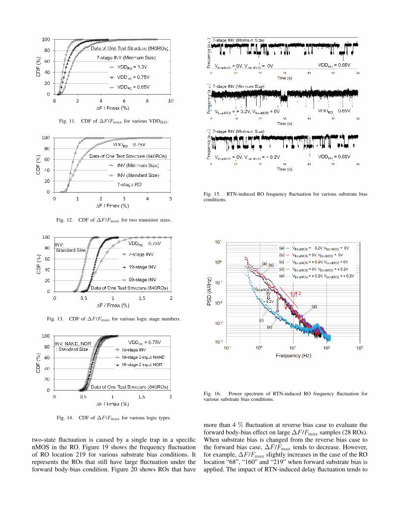
Fig. 5. Measurement results that shows 2-state fluctuation.
2 2
Fig. 6. PSD of Fig. 5
ec
Fig. 7. Time constant distribution of Fig. 5
oscillation frequency and ∆F is defined as the maximumfrequency fluctuation as shown in Fig. 4 (a). ∆F /Fmax isa good measure for the impact of RTN-induced frequencyfluctuation. It is 10.4 % for Fig. 4 (a). However, significantfluctuation is not observed for the case of Fig. 4 (b). Largefluctuation such as Fig. 4 (a) is a rare case that reflects theRTN nature. Figure 5 shows a typical measurement data at
S a m p l i n g P o i n tF requency( a .u .)
F r e q u e n c y ( a . u . )P opul ati on
F r e q u e n c y ( a . u . )Fig. 8. Estimation of discrete states by EM algorithm for a 2-state case.
F r e q u e n c y ( a . u . )P opul ati on
F r e q u e n c y ( a . u . )
S a m p l i n g P o i n tF requency( a .u .)
Fig. 9. Estimation of discrete states by EM algorithm for a complex case.
05 01 0 01 5 02 0 00 1 2 3 4 5 6 7 8 9 1 0 1 1 1 2P opul ati on
F / F m a x ( % )V D D R O = 0 . 6 5 VV b s & p M O S = 0 VV b s & n M O S = 0 VD a t a o f T h r e e T e s t S t r u c t u r e s ( 2 , 5 2 0 R O s )
R o o m T e m p e r a t u r e7 @ s t a g e I N V ( M i n i m u m S i z e ) 1 0 . 4 %Fig. 10. Histogram of measured ∆F /Fmax.
VDDRO=0.65V where a large 2-state fluctuation is observed.Time constants τc and τe are defined as the time that theRO stays at high-frequency state and low-frequency staterespectively. The power spectrum density (PSD) of Fig. 5 isobtained by quantizing the measurement data of Fig. 5 intothe 2-state waveform. Lorentzian power spectrum is observed(Fig. 6). Figure 7 shows time constant (τc, τe) distributionsof Fig. 5. It is found that both distributions for τc and τe
follow exponential distribution (e−t/τ ). Lorentzian PSD ande−t/τ distribution are observed for the case of a transistorwhere a single defect causes RTN fluctuation. This indicatesthat RTN fluctuation of Fig. 5 is caused by a single defectin a specific transistor in the 7-stage RO. Figure 8 and9 show the automatic discrete state estimation by the EM(Expectation Maximization) algorithm[15]. Figure 8 shows 2-state fluctuation. There are two peaks in the histogram. It isassumed to be composed of two normal distributions. Averagevalues of two normal distributions are identified with discretetwo states of RO oscillation by the EM algorithm. Figure 9shows the complex fluctuation. The EM algorithm works wellin such a complex case. It is possible to estimate discretestates of measurement data automatically by the EM method.Figure 10 shows the histogram of measured ∆F /Fmax for thewhole test structure of Fig. 3 over three chips (2,520 ROs). Itis found that the small number of samples have a large RTN-induced fluctuation and a long tail exists for larger ∆F /Fmax.
IV. IMPACT OF RTN ON DELAY UNCERTAINTY
Figure 11 shows the cumulative distribution function (CDF)of ∆F /Fmax for various VDDRO. The impact of RTN-induceddelay fluctuation increases rapidly under low voltage opera-tion. Figure 12 shows CDF of ∆F /Fmax for two transistorsizes. The ratio of nMOS gate area (W ×L) of the minimumsize inverter (INV) to the standard size INV is 0.30. The ratioof pMOS gate area of minimum INV to the standard INVis 0.21. Increasing the gate area slightly is very effective tosuppress the delay uncertainty. More than 50% reduction of∆F /Fmax can be achieved under 0.75V operation. Figure 13shows the CDF of ∆F /Fmax for various logic stage numbers.As the stage number decreases, the impact of RTN becomeslarger. Figure 14 shows the CDF of ∆F /Fmax for variouslogic types of 19-stage ROs. The impact of RTN is mostpronounced for the inverter case. Figure 15 shows the themeasurement results of frequency fluctuation of one RO forvarious substrate bias conditions. For this sample, the timeconstant is modulated considerably only when the pMOSsubstrate bias is changed from 0V to 0.2V. Figure 16 is thepower spectrum density (PSD) for the same sample of Fig. 15.RTN-induced RO frequency fluctuation for 60 s is evaluatedunder various substrate bias conditions. We observe the effectof one trap at the PMOS inside the RO that induces large delayfluctuation at the circuit level. Figure 17 shows the frequencyfluctuation of RO location (section No.) 1 for various substratebias. Four-state fluctuation due to two traps is clearly observedfor the normal substrate bias case. The effect of one of twotraps disappears for the forward bias case. Figure 18 shows thefrequency fluctuation of RO location 1 when pMOS or nMOSis forward biased. The effect of one of two traps disappearsonly when nMOS is forward biased. Thus the disappeared
02 04 06 08 01 0 00 2 4 6 8 1 0CDF(%)
F / F m a x ( % )123V D D R O = 0 . 6 5 VV D D R O = 0 . 7 5 VD a t a o f O n e T e s t S t r u c t u r e ( 8 4 0 R O s )V D D R O = 1 . 0 V7 4 s t a g e I N V ( M i n i m u m S i z e )
Fig. 11. CDF of ∆F /Fmax for various VDDRO.
02 04 06 08 01 0 00 1 2 3 4 5CDF(% )
F / F m a x ( % )12I N V ( S t a n d a r d S i z e )V D D R O = 0 . 7 5 VI N V ( M i n i m u m S i z e )D a t a o f O n e T e s t S t r u c t u r e ( 8 4 0 R O s )7 : s t a g e R O
Fig. 12. CDF of ∆F /Fmax for two transistor sizes.
02 04 06 08 01 0 00 0 . 5 1 1 . 5 2CDF(%)
F / F m a x ( % )1357 � s t a g e I N VV D D R O = 0 . 7 5 V
D a t a o f O n e T e s t S t r u c t u r e ( 8 4 0 R O s )I N V :S t a n d a r d S i z e 1 9 � s t a g e I N V5 9 � s t a g e I N V
Fig. 13. CDF of ∆F /Fmax for various logic stage numbers.
02 04 06 08 01 0 00 0 . 5 1 1 . 5 2CDF(% )
F / F m a x ( % )35 2V D D R O = 0 . 7 5 V1 9 " s t a g e I N V1 9 " s t a g e 2 " i n p u t N A N D1 9 " s t a g e 2 " i n p u t N O RD a t a o f O n e T e s t S t r u c t u r e ( 8 4 0 R O s )
I N V , N A N D , N O R: S t a n d a r d S i z eFig. 14. CDF of ∆F /Fmax for various logic types.
two-state fluctuation is caused by a single trap in a specificnMOS in the RO. Figure 19 shows the frequency fluctuationof RO location 219 for various substrate bias conditions. Itrepresents the ROs that still have large fluctuation under theforward body-bias condition. Figure 20 shows ROs that have
V b s � p M O S = 0 V , V b s � n M O S = 0 VV b s � p M O S = + 0 . 2 V , V b s � n M O S = 0 VV b s � p M O S = 0 V , V b s � n M O S = + 0 . 2 V
V D D R O = 0 . 6 5 VV D D R O = 0 . 6 5 VV D D R O = 0 . 6 5 V
7 � s t a g e I N V ( M i n i m u m S i z e )7 � s t a g e I N V ( M i n i m u m S i z e )7 � s t a g e I N V ( M i n i m u m S i z e )
Fig. 15. RTN-induced RO frequency fluctuation for various substrate biasconditions.
Fig. 16. Power spectrum of RTN-induced RO frequency fluctuation forvarious substrate bias conditions.
more than 4 % fluctuation at reverse bias case to evaluate theforward body-bias effect on large ∆F /Fmax samples (28 ROs).When substrate bias is changed from the reverse bias case tothe forward bias case, ∆F /Fmax tends to decrease. However,for example, ∆F /Fmax slightly increases in the case of the ROlocation “68”, “160” and “219” when forward substrate bias isapplied. The impact of RTN-induced delay fluctuation tends to

Fig. 17. RTN-induced RO frequency fluctuation for various substrate biasconditions (RO Location 1).
Fig. 18. RTN-induced RO frequency fluctuation for various substrate biasconditions (RO Location 1).
be reduced by forward body-biasing technique, but a few ROsdo not follow this tendency. Figure 21 shows the histogramof measured ∆F /Fmax for one test structure under varioussubstrate bias. The impact of RTN-induced delay fluctuationtends to be reduced by forward body-biasing technique, but afew ROs still have a large fluctuation.
V. CONCLUSIONS
Statistical nature of RTN-induced delay fluctuation is de-scribed by measuring 2,520 ROs fabricated in a commercial40 nm CMOS technology. The small number of samples havea large RTN-induced delay fluctuation. RTN-induced delayfluctuation becomes as much as 10.4% of nominal oscillationfrequency under low supply voltage (0.65V) operation. It isalso indicated that a single defect in a specific transistor
V b s � p M O S = 0 . 2 V , V b s � n M O S = 0 VV b s � p M O S = 0 V , V b s � n M O S = 0 V
V b s � p M O S = + 0 . 2 V , V b s � n M O S = + 0 . 2 V
R O L o c a t i o n : 2 1 9R O L o c a t i o n : 2 1 9R O L o c a t i o n : 2 1 9
Fig. 19. RTN-induced RO frequency fluctuation for various substrate biasconditions (RO Location 219).
01234567891 01 11 2
1 1 4 1 6 4 5 4 6 5 0 5 2 6 0 6 8 7 2 8 1 1 0 5 1 1 8 1 3 6 1 4 4F/F max(%)R O L o c a t i o n ( S e c t i o n N o . )
123
01234567891 01 11 2
1 5 4 1 5 8 1 6 0 1 6 6 1 7 3 2 0 7 2 1 9 2 2 2 2 3 2 2 3 4 2 9 2 2 9 3 2 9 7F/F max(%)R O L o c a t i o n ( S e c t i o n N o . )
123
V b s $ p M O S = 0 . 2 V , V b s $ n M O S = 0 VV b s $ p M O S = 0 V , V b s $ n M O S = 0 VV b s $ p M O S = + 0 . 2 V , V b s $ n M O S = + 0 . 2 V V D D R O = 0 . 6 5 VV D D R O = 0 . 6 5 VV b s $ p M O S = 0 . 2 V , V b s $ n M O S = 0 VV b s $ p M O S = 0 V , V b s $ n M O S = 0 VV b s $ p M O S = + 0 . 2 V , V b s $ n M O S = + 0 . 2 V
Fig. 20. ∆F /Fmax of different ROs for various substrate bias conditions. ROthat have more than 4% fluctuation at reverse substrate bias case are shown.
in an RO causes clear 2-state oscillation fluctuation. TheEM algorithm works well to identify discrete states for acomplex fluctuation as well as a simple 2-state one. Morethan 50% reduction of frequency uncertainty (∆F /Fmax) canbe achieved under 0.75V operation by slightly increasing thetransistor size. The impact of the parameters that can bechanged by circuit designers such as operating voltage, tran-
01 02 03 04 05 06 07 08 09 01 0 0
0 1 2 3 4 5 6 7 8 9 1 0P opul ati on
F / F m a x ( % )
123V b s ! p M O S = 0 . 2 V , V b s ! n M O S = 0 VV b s ! p M O S = 0 V , V b s ! n M O S = 0 VV b s ! p M O S = + 0 . 2 V , V b s ! n M O S = + 0 . 2 VV D D R O = 0 . 6 5 VD a t a o f O n e T e s t S t r u c t u r e
Fig. 21. Histogram of measured ∆F /Fmax for various substrate biasconditions.
sistor size, logic stage number, logic gate type, and substratebias is clarified in view of RTN-induced CMOS logic delayuncertainty.
ACKNOWLEDGMENTS
We are grateful to S. Fujimoto, K. Kitajima, I. Mahfuzul,T. Miki, S. Nishizawa for chip design. The VLSI chip in thisstudy has been fabricated in the chip fabrication program ofVLSI Design and Education Center (VDEC), the Universityof Tokyo in collaboration with STARC.
REFERENCES
[1] S. Borkar, “Designing reliable systems from unreliable components: thechallenges of transistor variability and degradation,” IEEE Micro, 25(2005) 10.
[2] M. Alam, “Reliability- and process-variation aware design of integratedcircuits,” Microelectron. Reliab., 48 (2008) 1114.
[3] H. Onodera, “Variability modeling and impact on design,” IEDM Tech.Dig., 2008, p. 701.
[4] M. J. Kirton and M. J. Uren, “Noise in solid-state microstructures: Anew perspective on individual defects, interface states and low-frequency(1/f) noise,” Adv. Phys., 38 (1989) 367.
[5] D. K. Schroder and J. A. Babcock, “Negative bias temperature instabil-ity: Road to cross in deep submicron silicon semiconductor manufac-turing,” J. Appl. Phys., 94 (2003) 1.
[6] J. H. Sthathis and S. Zafar, “The negative bias temperature instabilityin MOS devices: A review,” Microelectron. Reliab., 46 (2006) 270.
[7] M. Alam, “A critical examination of the mechanics of dynamic NBTIfor PMOSFETs,” IEDM Tech. Dig., 2003, p. 345.
[8] X. Wang, P. Rao, A. Mierop, A. Theuwissen, “Random Telegraph Signalin CMOS Image Sensor Pixels,” IEDM Tech. Dig., 2006, p. 115.
[9] H. Kurata, K. Otsuga, A. Kotabe, S. Kajiyama, T. Osabe, Y. Sasago, S.Narumi, K. Tokami, S. Kamohara, O. Tsuchiya, “Random TelegraphSignal in Flash Memory: Its Impact on Scaling of Multilevel FlashMemory Beyond the 90-nm Node,” IEEE J. Solid-State Circuits, 42(2007) 1362.
[10] M. Yamaoka, H. Miki, A. Bansal, S. Wu, D. Frank, E. Leobandung, K.Torii, “Evaluation Methodology for Random Telegraph Noise Effects inSRAM arrays,” IEDM Tech. Dig., 2011, p. 745.
[11] K. Takeuchi, T. Nagumo, and T. Hase: “Comprehensive SRAM DesignMethodology for RTN Reliability,” IEEE Symposium on VLSI Tech-nology, 2011, p. 130.
[12] K. Takeuchi, T. Nagumo, K. Takeda, A. Asayama, S. Yokogawa, K.Imai, and Y. Hayashi: “Direct Observation of RTN-induced SRAMFailure by Accelerated Testing and Its Application to Product ReliabilityAssessment,” IEEE Symposium on VLSI Technology, 2010, p. 189.
[13] K. Ito, T. Matsumoto, S. Nishizawa, H. Sunagawa, K. Kobayashi and H.Onodera, “The Impact of RTN on Performance Fluctuation in CMOSLogic Circuits,” Proc. IRPS, 2011, p. 710.
[14] T. Matsumoto, K. Kobayashi and H. Onodera, “Impact of RandomTelegraph Noise on CMOS Logic Delay Uncertainty under Low VoltageOperation,” IEDM Tech. Dig., 2012, p. 581.
[15] A. Dempster, N. Laird, D. Rubin, “Maximum Likelihood from Incom-plete Data via the EM Algorithm,” J. of the Royal Statistical Society.Series B (Methodological), 39 (1977) 1.