implementation of a direction finding algorithm on …
TRANSCRIPT

IMPLEMENTATION OF A DIRECTION FINDING ALGORITHM ON AN FPGA PLATFORM
A THESIS SUBMITTED TO THE GRADUATE SCHOOL OF NATURAL AND APPLIED SCIENCES
OF MIDDLE EAST TECHNICAL UNIVERSITY
BY
ABDULLAH VOLKAN İPEK
IN PARTIAL FULFILLMENT OF THE REQUIREMENTS FOR
THE DEGREE OF MASTER OF SCIENCE IN
ELECTRICAL AND ELECTRONICS ENGINEERING
OCTOBER 2006

Approval of the Graduate School of (Name of the Graduate School)
Prof. Dr. Canan ÖZGEN Director
I certify that this thesis satisfies all the requirements as a thesis for the degree of Master of Science.
Prof. Dr. İsmet ERKMEN Head of Department
This is to certify that we have read this thesis and that in our opinion it is fully adequate, in scope and quality, as a thesis for the degree of Master of Science.
Prof. Dr. Mete SEVERCAN Supervisor
Examining Committee Members (first name belongs to the chairperson of the jury and the second name belongs to supervisor) Prof. Dr. Yalçın TANIK (METU, EE)
Prof. Dr. Mete SEVERCAN (METU, EE)
Assoc. Prof. Dr. Sencer KOÇ (METU, EE)
Assist. Prof. Dr. Çağatay CANDAN (METU, EE)
Ülkü DOYURAN (ASELSAN)

iii
I hereby declare that all information in this document has been obtained and
presented in accordance with academic rules and ethical conduct. I also declare
that, as required by these rules and conduct, I have fully cited and referenced
all material and results that are not original to this work.
Name, Last name : Abdullah Volkan İPEK
Signature :

iv
ABSTRACT
IMPLEMENTATION OF A DIRECTION FINDING ALGORITHM ON AN FPGA PLATFORM
İPEK, Abdullah Volkan
M.S., Department of Electrical and Electronics Engineering
Supervisor : Prof. Dr. Mete SEVERCAN
October 2006, 83 pages
In this thesis work, the implementations of the monopulse amplitude comparison and
phase comparison DF algorithms are performed on an FPGA platform. After the
mathematical formulation of the algorithms using maximum-likelihood approach is
done, software simulations are carried out to validate and find the DF accuracies of
the algorithms under various conditions. Then the algorithms are implemented on an
FPGA platform by utilizing platform specific software tools. Block diagrams of the
hardware implementations are given and explained in detail. Then simulations of
hardware implementation of both algorithms are performed. Using the results of the
simulations, DF accuracies under certain conditions are evaluated and compared to
software simulations results.
Keywords: Direction Finding, Amplitude Comparison, Phase Comparison, Interferometer, FPGA

v
ÖZ
YÖN BULMA ALGORİTMASININ FPGA PLATFORMUNDA UYGULANMASI
İPEK, Abdullah Volkan
Yüksek Lisans Tezi, Elektrik ve Elektronik Mühendisliği Bölümü
Tez Yöneticisi : Prof. Dr. Mete SEVERCAN
Ekim 2006, 83 sayfa
Bu tez çalışmasında, genlik karşılaştırmalı ve faz karşılaştırmalı yön bulma
algoritmaları FPGA platformunda gerçeklenmiştir. Maksimum olabilirlik yaklaşımı
kullanılarak algoritma matematiksel olarak formüle edildikten sonra, yazılım
benzetimleri yapılarak algoritma geçerli kılınmış, farklı durumlarda algoritmaların
yön bulma doğrulukları bulunmuştur. Daha sonra platforma özel yazılım araçları
kullanılarak algoritmalar FPGA platformunda uygulanmıştır. Donanım
uygulamalarının blok şemaları verilerek detaylı bir şekilde anlatılmıştır. Her iki
algoritmanın donanım uygulamasının benzetimi yapılmıştır. Benzetim çalışmalarının
sonuçları kullanılarak belirli koşullar altındaki yön bulma doğruluğu
değerlendirilmiş, yazılım benzetim sonuçları ile karşılaştırılmıştır.
Anahtar Kelimeler: Yön Bulma, Genlik Karşılaştırma, Faz Karşılaştırma, FPGA

vi
To My Parents and To My Lovely Sister

vii
ACKNOWLEDGMENTS
I would like to thank Prof. Dr. Mete Severcan for his valuable supervision, support
and tolerance throughout the development and improvement of this thesis.
I am grateful to Turgut Çelikadam, Metin Şengül and Serkan Sevim for their support
throughout the development and the improvement of this thesis. I am also grateful to
Aselsan Electronics Industries Inc. for the resources and facilities that I use
throughout thesis.
Thanks a lot to all my friends for their great encouragement and their valuable help
to accomplish this work.
Lastly, I would like to thank my parents for bringing up and trusting in me, and
Demet Salman, for giving me the strength and courage to finish this work.
viii
TABLE OF CONTENTS
ABSTRACT ........................................................................................................... iv
ÖZ ............................................................................................................................v
ACKNOWLEDGMENTS...................................................................................... vii
TABLE OF CONTENTS...................................................................................... viii
LIST OF TABLES....................................................................................................x
LIST OF FIGURES ................................................................................................ xi
LIST OF ABBREVIATIONS ................................................................................xiv
CHAPTERS
1. INTRODUCTION ................................................................................................1
1.1 Direction Finding ......................................................................................1
1.2 The meaning of Monopulse .......................................................................2
1.3 Monopulse DF Systems.............................................................................3
1.3.1 Amplitude Comparison DF Systems ..................................................3
1.3.2 Interferometer DF Techniques ...........................................................4
1.4 Description of the Thesis ...........................................................................7
1.5 Outline of the Thesis .................................................................................7
2. DF ALGORITHMS ..............................................................................................8
2.1 Amplitude Comparison Algorithm.............................................................8
2.2 Phase Comparison Algorithm ..................................................................11
3. IMPLEMENTATION.........................................................................................15
3.1 Amplitude Comparison............................................................................15
3.1.1 Software Simulation Results ............................................................17
3.1.1.1 1st Approach ................................................................................17
3.1.1.2 2nd Approach................................................................................20
3.1.1.3 Comparison of Approaches..........................................................23
3.1.2 Hardware Implementation................................................................24
3.1.2.1 Hardware Design .........................................................................25

ix
3.1.2.1.1 AC_Angle_Counter Block .....................................................26
3.1.2.1.2 AC_Correlation_Computation Block......................................31
3.1.2.1.3 AC_AOA_Estimator Block....................................................33
3.1.2.2 Simulation Results .......................................................................34
3.2 Phase Comparison ...................................................................................39
3.2.1 Software Simulation Results ............................................................44
3.2.2 Hardware Implementation................................................................52
3.2.2.1 Hardware Design .........................................................................53
3.1.2.1.4 PC_Angle_Counter Block ......................................................54
3.1.2.1.5 PC_Address_Decode Block ...................................................55
3.1.2.1.6 PC_Function_Calculation Block ............................................56
3.1.2.1.7 PC_AOA_Estimator Block.....................................................58
3.2.2.2 Simulation Results .......................................................................59
3.2.2.3 Part of PDW Generator Design ....................................................63
3.2.2.3.5 I_ Q_Demodulator Block .......................................................64
3.2.2.3.6 Magnitude_Calculator Block..................................................67
3.2.2.4 Simulation Results .......................................................................68
4. CONCLUSIONS ................................................................................................70
REFERENCES .......................................................................................................73
APPENDICES........................................................................................................75
APPENDIX A ........................................................................................................75
A.1 Antenna Gain Pattern ...................................................................................75
APPENDIX B.........................................................................................................77
B.1 FPGA’s ........................................................................................................77
APPENDIX C.........................................................................................................80
C.1 Development Tool Flow ...............................................................................80
C.2 Xilinx System Generator ..............................................................................80

x
LIST OF TABLES
Table 3-1 Mean and Standard Deviation of RMS Error (1st Approach)....................20
Table 3-2 Mean and Standard Deviation of RMS Error (2nd Approach)...................22
Table 3-3 Mean and Standard Deviation of RMS Error for Amplitude Comparison
Hardware Implementation.......................................................................................37
Table 3-4 FPGA Resource Utilization Summary of Amplitude Comparison
Implementation.......................................................................................................38
Table 3-5 FPGA Resource Utilization Summary of Phase Comparison
Implementation.......................................................................................................62
Table 3-6 Mean and Standard Deviation of RMS Error of Estimated AOA ............69

xi
LIST OF FIGURES
Figure 1.1 Harmonic Binary Related Interferometer..................................................5
Figure 2.1 Circular Array Geometry (N=6) ...............................................................8
Figure 2.2 Phase Array Geometry ...........................................................................11
Figure 3.1 Block Diagram of the Amplitude Comparison DF System......................16
Figure 3.2 Amplitude Comparison Antenna Gain vs. Angle ....................................17
Figure 3.3 RMS Error vs. AOA (SNR is equal to 10dB and 15dB)..........................18
Figure 3.4 RMS Error vs. AOA (SNR is equal to 20dB, 25dB and 30dB) ...............19
Figure 3.5 RMS Error vs. AOA (SNR is equal to 35dB and 40dB)..........................19
Figure 3.6 RMS Error vs. AOA (SNR is equal to 10dB and 15dB)..........................21
Figure 3.7 RMS Error vs. AOA (SNR is equal to 20dB, 25dB and 30dB ) ..............21
Figure 3.8 RMS Error vs. AOA (SNR is equal to 35 dB and 40dB).........................22
Figure 3.9 Mean of RMS Error vs. SNR..................................................................24
Figure 3.10 Block Diagram of the Amplitude Comparison Implementation.............26
Figure 3.11 Logic Diagram of AC_Angle_Counter Block.......................................27
Figure 3.12 Logic Diagram of AC_Max_Amplitude_Finder Block .........................28
Figure 3.13 Logic Diagram of AC_Max_PA_Selector Block ..................................29
Figure 3.14 Logic Diagram of AC_Address_Counter Block....................................30
Figure 3.15 Search Interval for Amplitude Comparison Implementation .................31
Figure 3.16 Logic Diagram of the AC_Correlation_Computation Block .................31
Figure 3.17 Logic Diagram of AC_AOA_Estimator Block .....................................33
Figure 3.18 Screen Shot from System Generator (Implementation of Amplitude
Comparison) ...........................................................................................................35
Figure 3.19 RMS Error vs AOA of Amplitude Comparison Hardware
Implementation at 20dB SNR .................................................................................36
Figure 3.20 RMS Error vs AOA of Amplitude Comparison Hardware
Implementation at 30dB SNR .................................................................................36
Figure 3.21 Block diagram of the Phase Comparison DF system.............................39

xii
Figure 3.22 Single Baseline Interferometer .............................................................40
Figure 3.23 Phase Comparison Antenna Layout......................................................41
Figure 3.24 Real and Imaginary parts of Phase Comparison for d/λ=2 ...................42
Figure 3.25 Phase Comparison Antenna Gain and Phase Pattern for d/λ=2..............43
Figure 3.26 Typical Plot of ( )φ'J vs. AOA for 1/ =λd and 5/ =λd (AOA=35) ...43
Figure 3.27 Search Interval for Phase Comparison..................................................44
Figure 3.28 Phase Comparison RMS Error vs. AOA at λ/d value from 1 to 5 in
steps of 0.5 (SNR = 10 dB) ....................................................................................45
Figure 3.29 Phase Comparison RMS Error vs. AOA at λ/d value from 1 to 5 in
steps of 0.5 (SNR = 20 dB) ....................................................................................46
Figure 3.30 Phase Comparison RMS Error vs. AOA at λ/d value from 1 to 5 in
steps of 0.5 (SNR = 30 dB) .....................................................................................46
Figure 3.31 Mean of RMS Error vs. λ/d Values for SNR=10dB, 20dB and 30dB .47
Figure 3.32 RMS Error vs. AOA when Frequency is varied from 2 GHz to 6 GHz in
steps of 500MHz at SNR = 20dB. ...........................................................................49
Figure 3.33 Mean of the RMS Error vs. Frequency at SNR=20dB...........................49
Figure 3.34 The RMS Error vs. Frequency when fresolution = 100 MHz
(AOA=30 degrees)..................................................................................................51
Figure 3.35 The RMS Error vs. Frequency when fresolution = 50 MHz
(AOA=30 degrees)..................................................................................................51
Figure 3.36 The RMS Error vs. Frequency when fresolution=64 MHz
(AOA=30 degrees)..................................................................................................52
Figure 3.37 Block Diagram of Phase Comparison Implementation..........................53
Figure 3.38 Logic Diagram of the PC_Angle_Counter Block..................................54
Figure 3.39 Logic Diagram of the PC_Address_Decoder Block..............................55
Figure 3.40 Logic Diagram of PC_Function Calculation Block...............................56
Figure 3.41 Logic Diagram of Complex_Multiplier_1 Block ..................................57
Figure 3.42 Logic Diagram of Complex_Multiplier_2 Block ..................................58
Figure 3.43 Logic Diagram of the PC_AOA_Estimator Block ................................58
Figure 3.44 Screen Shot from System Generator (Implementation of Phase
Comparison Algorithm) ..........................................................................................59

xiii
Figure 3.45 Phase Comparison Hardware Implementation RMS Error vs. AOA
(SNR=20dB)...........................................................................................................60
Figure 3.46 Mean and The Standard Deviation of RMS Error .................................61
Figure 3.47 Mean of the Estimated AOA vs. Frequency..........................................61
Figure 3.48 RMS Error of Hardware Implementation due to
Frequency Quantization ..........................................................................................62
Figure 3.49 Block Diagram of Phase Comparison Implementation..........................64
Figure 3.50 I and Q Demodulation ..........................................................................65
Figure 3.51 Logic Diagram of I and Q Demodulator Block .....................................65
Figure 3.52 Magnitude Response of FIR Filter (Hilbert Transformation) ................66
Figure 3.53 Magnitude Response of FIR LPF .........................................................66
Figure 3.54 Logic Diagram of Magnitude_Calculator Block ...................................67
Figure 3.55 Block Diagram of the Phase Comparison Implementation ....................68
Figure A.1 Generated Antenna Pattern for Amplitude Comparison .........................76
Figure B.1 Virtex Family FPGA Logic Slice...........................................................78
Figure C.1 Function Block Parameters of a Xilinx Multiplier Block........................82

xiv
LIST OF ABBREVIATIONS
AC : Amplitude Comparison
ADC : Analog to Digital Converter
AOA : Angle of Arrival
CW : Continuous Wave
DF : Direction Finding
DOA : Direction of Arrival
DSP : Digital Signal Processing
ESM : Electronic Support Measures
FIR : Finite Impulse Response
FPGA : Field Programmable Gate Arrays
GSPS : Giga Samples per Second
LPF : Low Pass Filter
MPPS : Mega Pulse per Second
MSPS : Mega Samples per Second
PC : Phase Comparison
PDW : Pulse Descriptor Word
PRI : Pulse Repetition Interval
RF : Radio Frequency
RMS : Root Mean Square
RWR : Radar Warning Receivers
SNR : Signal to Noise Ratio
TOA : Time of Arrival
UCA : Uniform Circular Array
ULA : Uniform Line Array
CHAPTER I
INTRODUCTION
1.1 Direction Finding
The ultimate aim for the Electronic Support Measurement (ESM) system is to
identify the RF guided weapon. The general procedure of the identification against
RF guided weapons can be summarized as follows. First the ESM system intercepts
the radiations associated with that weapon, and then separates these signals from
other intercepted signals. Then the parameters of the selected signals are measured.
ESM system compares the parameters against a stored set of parameters to identify
the type of the sensor. Finally the weapon is identified by previously identified
definitions of the weapons. In the process of identifying the RF guided weapon, the
ESM system provides information on the angular direction of the intercepted signal
[1]. A direction finder is a passive device that determines the direction/angle of
arrival (DOA/AOA) of radio-frequency energy [2]. Determining the DOA or AOA
of signal is fundamental to ESM systems, since emitters cannot change on pulse to
pulse basis.
Purpose of direction finding operations is to detect the position of the emitter, which
can be calculated from the bearings of several direction finders. There are many
factors that should be considered in direction finding problem. Choice of the array
geometry and antennas, the receiver structure and the optimum algorithm that is
employed can be considered as main factors. Obviously the interactions between
these parts must not be ignored.
The antenna pattern and polarization are important parameters that affect the DF
accuracy of the system. In DF systems, multiple antennas are arranged in various
geometrical configurations. Array geometry affects various aspects of the DF system
such as resolution, sensitivity to system errors and the type of processing used to

2
produce DOA estimates. In most arrays, the elements of an array are identical, which
is often more convenient, simpler, and more practical. The most commonly
considered structures are the linear and circular arrays. Antenna spacing over the
specified geometry can be selected to be uniform or non-uniform. Uniform Line
Array (ULA) is implemented with inter-element spacing less than or equal to λ/2;
where λ is the wavelength at the center frequency. The importance of non-uniform
line array structures is that they are considerably more robust as compared to ULA’s
with respect to their radiation characteristics. A linear array does not provide uniform
resolution capability over the entire horizon. One of the main advantages of a
circular array over linear arrays is its 360º azimuthal coverage which is very
important especially in ESM applications. The structure which the elements are
arranged uniformly around 360º in azimuth is called as a uniform circular array
(UCA). UCA geometry is one of the most commonly used array geometry in DF
systems [3].
There are various approaches to estimate the angular location of the emitter. The
most commonly used methods are monopulse and high resolution methods. High
resolution methods are more complex compared to monopulse. They are based on
correlation matrix, eigenvalue and eigenspace computations. Computational costs of
these methods are higher, which is an important drawback for many practical
systems. On the other side, monopulse systems should operate in real time, provide
fast responses, and be able to process as large as pulses per second to find the AOA.
1.2 The meaning of Monopulse
It is stated in [4] that the word monopulse was first introduced by H.T. Budenbom of
the Bell Telephone Laboratories in 1946. It is a hybrid word, because mono meaning
one comes from Greek, while pulse comes from Latin. It becomes very common
because it clearly expressed the ability to collect, from each pulse, the information
needed for a pair of two coordinate angle estimates, whereas the older angle-sensing
techniques of conical scan and lobe switching required several (at least four) pulses
to form a pair of angle estimates.

3
The term simultaneous lobing, synonymous with monopulse, is a more accurate
description of the technique, although it is less commonly used. It is the simultaneity
rather than “one pulse” that is essential. As a matter of fact, most monopulse radars
do not extract angle estimates from each pulse. The usual practice is to smooth or
integrate the raw single-pulse signals over some interval before forming the angle
estimates. Furthermore, monopulse is not confined to pulsed radars. It can be used
just as well in Continuous Wave (CW) or modulated CW radars. It can be used
passive mode to track a source of signals or noise such as transmitting antenna, a
jammer or the sun [4].
1.3 Monopulse DF Systems
The two primary techniques used for monopulse direction finding are the amplitude-
comparison method and the interferometer or phase comparison method. The phase-
comparison method generally has the advantage of greater accuracy, but the
amplitude-comparison method is used extensively due to its lower complexity and
cost. In the following chapters, information about amplitude and phase comparison
systems will be given.
1.3.1 Amplitude Comparison DF Systems
Virtually all currently deployed radar warning receiving (RWR) systems use
amplitude-comparison direction finding. A basic amplitude-comparison receiver
derives a ratio, and ultimately angle-of-arrival or bearing, from a pair of independent
receiving channels, which utilize squinted antenna elements that are usually
equidistantly spaced to provide an instantaneous 360º coverage. Typically, four or
six antenna elements and receiver channels are used in such systems, and wideband
logarithmic video detectors provide the signals for bearing-angle determination. The
monopulse ratio is obtained by subtraction of the detected logarithmic signals, and
the bearing is computed from the value of the ratio [1].
In amplitude comparison, typically broadband spiral antenna elements whose
patterns can be approximated by Gaussian-shaped beams are used. Gaussian-shaped

4
beams have the property that the logarithmic output ratio slope in dB is linear as a
function of angle of arrival. Thus, a digital look-up table can be used to determine the
angle directly. However, both the antenna beamwidth and squint angle vary with
frequency over the multi-octave bands used in RWRs. Pattern shape variations cause
a larger pattern crossover loss for high frequencies and reduced slope sensitivity at
low frequencies. Partial compensation of these effects, including antenna squint, can
be implemented using a look-up table if frequency information is available in the
RWR. Otherwise, gross compensation can be made, depending upon the RF octave
band utilized [1].
It is stated in [5] that the typical accuracies can be expected to range from 3 to 10
degrees RMS for multi-octave frequency band amplitude-comparison systems which
cover 360 degrees with four to six antennas. The four-quadrant amplitude-
comparison DF systems employed in RWRs have the advantage of simplicity,
reliability, and low cost. Usually, only one antenna per quadrant is employed which
covers the 2 to 18 GHz band. The disadvantages are poor accuracy and sensitivity,
which result from the broad-beam antennas employed. Both accuracy and sensitivity
can be improved by expanding the number of antennas employed. For example,
expanding to eight antennas would double the accuracy and provide 3 dB more gain.
As the number of antennas increases, it becomes appropriate to consider multiple-
beam-forming antennas rather than just increasing the number of individual antennas.
1.3.2 Interferometer DF Techniques
Interferometer can be considered as specific cases of antenna arrays. All antenna
elements center may lie in a straight line at equal spacing (ULA) or at different
spacing to obtain time of arrival (TOA) difference of the incoming waves. The
difference of TOA will lead to a measurable phase difference, which is used for
determination of the angle of arrival (AOA) information. The concept of using phase
difference of the received signals can be used with circular array structures to cover
360 degrees azimuth from antennas mounted at a point.

5
Interferometer system antennas typically use broad antenna beams with beamwidths
of the order 90 degrees. It is stated in [1] that the lack of directivity produces several
deleterious effects. First, it limits the system sensitivity due to reduced antenna gain.
Second, it open the system to interference signals often include multipath from
strong signals which can limit the accuracy of the interferometer.
An interferometer system consisting of two antennas in space causes an ambiguity in
determination of AOA. The system has coverage of 180 degrees in azimuth; however
it is not clear from which half of the hemisphere the signal originated. Practical
interferometer systems solve this problem by using another system such as an
amplitude monopulse DF system to select proper estimate of DOA or use quadrant
arrays of antennas shielded from each other, or a circular array of monopulses to
cover a 360 degree field of view [6]. Another method to resolve ambiguities is to use
a multiple antenna elements, called multiple baseline interferometers. In a typical
design of multiple baseline interferometers, there exists a reference antenna and a
series of companion antennas, spaced in line and located at different distances from
the reference antenna in order to operate together.
In multiple baseline interferometer systems, there are two types of choice of antenna
element location. A harmonic binary related interferometer system divides each
aperture baseline by a factor of 2 is given in Figure 1.1.
Figure 1.1 Harmonic Binary Related Interferometer

6
The number of ambiguities is increased as the spacing to the reference antenna is
increased. In the selected quadrant, first antenna pair, forming a 2/λ baseline,
solves the ambiguity problem and determines the AOA, and then the next pair
improves the resolution and achieves a better determination. The process continues
up to longest baseline.
In non-harmonic related spaced antennas, the antenna element spacing, which is not
necessarily 2/λ , is determined up to frequency to solve the ambiguity problem. In
this configuration, ambiguities will be presented at many frequencies. Nevertheless,
knowledge of spacing or spacing ratios and the frequency of the incoming signal and
utilization of look up tables and some logic algorithms, the angle of arrival can be
determined.
The non-harmonic related spacing is more preferred to harmonic-binary related
spacing antennas, since it has a wide RF bandwidth of coverage. And the binary
system is limited at the high-end frequency range to half-wavelength baseline
spacing. Also it is stated in [3] that the performance of uniform and different non-
uniform LA structures are compared, and in the event of single target in additive
white Gaussian noise, the non uniform arrays found to provide significant
improvement over arrays of the same number of elements which shows the
importance of array geometry.
When high DF accuracy is needed in an interferometer system, alternatively antenna
baseline spacing can be increased. The increased baseline spacing results in multi-
lobe structures along the coverage range, which requires less signal to noise ratio
(SNR) to achieve same the DF accuracy. For a two element interferometer with 16 λ
spacing would end up 33 lobes through ±90 degree azimuth coverage. Within the 33
lobes, it would only require a SNR of 20dB to achieve 0.1 degree accuracy [1].
Although there are 33 ambiguous regions on the coverage range, ambiguity will be
resolved by employing a third antenna element with 2/λ baseline spacing. At the
defined SNR value, it will provide a DF accuracy of 3 degrees, which is sufficient to
solve the ambiguity [1].

7
1.4 Description of the Thesis
In this work, two algorithms based on monopulse DF techniques, namely amplitude
comparison and phase comparison, to solve the problem of estimating direction of
arrival (DOA) of plane waves impinging on the antennas from unknown direction are
employed. The sources and the antennas are assumed to be coplanar, and therefore,
the problem is constrained to estimate the DOA’s in azimuth only. Amplitude
comparison and phase interferometer techniques are studied in this work by
employing maximum likelihood estimation approach. The algorithms are
implemented on an FPGA platform and simulation results are obtained by varying
parameters such as SNR, baseline spacing etc. The implementation details of the
design, discussions and comparisons of the simulation results of the algorithms are
explained in detail.
1.5 Outline of the Thesis
This thesis is organized as follows: In Chapter II, the problem is stated and
formulated; the amplitude comparison and phase interferometer DF algorithms based
on ML estimation are developed and described in detail.
In Chapter III, in order to investigate the performance of the proposed algorithms, the
root-mean-square (RMS) errors at different angles and various conditions are
calculated. Typical results of the software simulations are presented, along with the
discussions related to the effects of different parameters. Some practical limitations,
assumptions, modifications and practical advantages related to the implementation of
this algorithm on an FPGA platform are also discussed. The results of the
implementation are compared with the expected values.
Finally, both monopulse DF algorithms are summarized. Moreover some concluding
remarks of these algorithms and hardware implementations are discussed in Chapter
IV.

8
CHAPTER II
DF ALGORITHMS
2.1 Amplitude Comparison Algorithm
The DF system considered in this part consists of a circular array of N equally spaced
antennas. It is assumed that there is a single transmitter and the signal arrives at the
antenna at angle of θ . The geometry of the antennas (for N=6) is given in Figure 2.1.
Figure 2.1 Circular Array Geometry (N=6)

9
The received signal is defined by
( ) iiii nARs +−= θθ (2-1)
where θ and A represents AOA and amplitude of the incoming signal respectively.
( )iR denotes the power pattern of the antenna, iθ is the angular position of the ith
(i=1,2…N) antenna, which is given by ( )( )1/2 −iNπ and ni is the receiver noise.
In this case, the problem is to estimate θ by using observations of the received
signals si’s. At that point, two assumptions are made. First assumption is that the
additive noise is assumed to be white Gaussian noise of variance 2σ . Second one is
that the additive noise of each receiver channel is independent of each other. The
Gaussian distributed random variable having zero mean and a variance of 2σ has the
density function of the form
( ) 2
2
2
22
1σ
πσ
x
exf−
= (2-2)
Since random variables are independent from each other, their joint density function
is the product of the densities for each Gaussian variable. The probability density
function (pdf) can be expressed as
( )( )( )
2
2
2
122
1, σ
θθ
πσθ
iii ARsN
i
eAf
−−−
=
∏= (2-3)
The maximum likelihood estimation for parameter θ is the estimate, which
maximizes the joint density function.
( )( )θθθ
,maxarg Af= (2-4)
Maximizing the maximum likelihood function is equivalent to minimizing the
negative of logarithm of it, since the maximum likelihood function is a monotonic
function. By eliminating constant terms, the equation can be rewritten as
( )( )∑−
=
−−=1
0
2),(N
i
iii ARsAJ θθθ (2-5)

10
Therefore the estimate θ can be obtained by minimizing J as
( )( )θθθ
,minarg AJ= (2-6)
The maximum likelihood estimation is function of A andθ . In order to find the
minimum point of the function, a derivative with respect to A is taken and set to
zero. Taking derivative of Eq.(2-5) with respect to A yields to
( ) ( )( ) 022),( 1
0
2 =−+−−=∂
∂∑
−
=
N
i
iiiii ARRsA
AJθθθθ
θ (2-7)
( )( )
( )∑
∑−
=
−
=
−
−
=1
0
2
1
0ˆN
i
ii
N
i
iii
R
Rs
A
θθ
θθ
(2-8)
Substituting the estimate of A in Eq.(2-5) yields to
( )
( )∑
∑∑ −
=
−
=−
= −
−
−=1
0
2
21
01
0
2)(N
i
ii
N
i
iiiN
i
i
R
Rs
sJ
θθ
θθ
θ (2-9)
Since main concern is the minimization of the Eq.(2-9) with respect to θ , the first
term, which is not a function of θ , can be eliminated. Rearranging the equation
yields
( )( )
( )∑
∑−
=
−
=
−
−
=1
0
2
21
0
N
i
ii
N
i
iii
R
Rs
M
θθ
θθ
θ (2-10)
The AOA can be estimated by the value that maximizes ( )θM .
( )( )θθθ
Mmaxarg= (2-11)

11
2.2 Phase Comparison Algorithm
The DF system considered in this study consists of a linear phase array of two
antennas, which are assumed to have identical gain patterns. The array geometry of
the antennas is given in Figure 2.2.
x
dsin(φ)
φ
φ
Figure 2.2 Phase Array Geometry
The signals arriving to antennas at angle ofφ are given by
1)( ngAesj += φθ (2-12)
2)( ngeAedjj += φψθ (2-13)
where, A is the amplitude and θ is the phase of the incoming signal, ψ is the phase
difference between the signals arriving to the antennas, )(φg is the antenna pattern
and in is the receiver noise of the ith antenna (i=1, 2).

12
In order to make Eq.(2-13) more compact, )(φh is defined as
)()( φφ ψgeh
j= (2-14)
Substituting Eq.(2-14) in Eq.(2-12) and Eq.(2-13), received signals are redefined as
1)( ngAesj += φθ (2-15)
2)( nhAedj += φθ (2-16)
The additive noise in (i=1, 2) is assumed to be white Gaussian noise with noise
samples being independent of each other and having identical variances 2σ . The
Gaussian distributed random variable having zero mean and a variance of 2σ has the
density function given in Eq.(2-2). In this case, there are two independent random
variables. Therefore their joint density function is the product of the densities for
each Gaussian variable. The probability density function (pdf) is given by
( )( ) ( )
2
2
2
2
2
2
2
2 2
1
2
1,, σ
φ
σ
φ θθ
πσπσφθ
hAedgAesjj
eeAf
−−
−−
= (2-17)
The principle is the same for all maximum likelihood estimation problems. The
maximum likelihood estimate for parameter φ is the one which makes the given
observations the most likely. In other words, it is the value that maximizes ( )φθ ,,Af .
( )( )φθφϕ
,,maxarg Af= (2-18)
Since logarithm is a monotonic function, maximizing the Eq. (2-17) is equivalent to
minimizing the negative logarithm of the likelihood function. By eliminating
constant terms of the function, the maximum likelihood function becomes
( )22
)()(,, φφφθ θθhAedgAesAJ
jj −+−= (2-19)

13
Now the maximum likelihood problem can be estimated by the value that
minimizes ( )φθ ,,AJ .
( )( )φθφφ
,,min AJrga= (2-20)
As it is observed in Eq.(2-19), the maximum likelihood estimation function is a
function of A, θ and φ . To estimate AOA, derivatives of the function must be taken
with respect to A, θ and set to 0.
Taking derivate of ( )φθ ,,AJ with respect to A and setting to 0 yields to
( ) ( ) }{ }{ 0)(Re2)(Re222),,( **22
=−−+=∂
∂ −− φφφφφθ θθ
hdegsehAgAA
AJ jj (2-21)
( ){ } ( )}{( ) ( ) 22
*-j*-j
||||
.hd.eRe .gs.eReˆφφ
φφ θθ
hgA
+
+= (2-22)
Taking derivate of ( )φθ ,,AJ with respect toθ and setting to 0 yields to
( ) ( )( ) ( ) ( )( ) hed + h(se ges + g(se),,( j**j-j**j- φφ
θφφ
θθ
φθ θθθθ
∂
∂−
∂
∂−=
∂
∂ AJ=0 (2-23)
Simplifying and rearranging the terms yields to
( )}{ 0)()(Im ** =+− φφθdhsge
j (2-24)
Since the imaginary part of the equation is zero, it can be rewritten as
πθφφ jkjKedhsg
+=+ )()( ** (2-25)
The estimated value of θ can be simplified as
( ) ( )( )φφθ **argˆ dhsg += (2-26)
The estimate of A can be further simplified by substituting Eq.(2-26) in Eq.(2-22) as
( ) ( )
( ) ( ) 22
**
||||
dhsgˆ
φφ
φφ
hgA
+
+= (2-27)

14
Substituting the estimate of A found in Eq.(2-27) in ),,( φθAJ , rearranging and
simplifying gives
( )( ) ( )
( ) ( ) 22
2**22
||||
dhsg,,
φφ
φφφθ
hgdsAJ
+
+−+= (2-28)
Since the magnitude of the complex signals are constant and constitute a DC value,
the equation can be further simplified by eliminating the constant non-negative
terms.
( )( ) ( )
( ) ( ) 22
2**
/
||||
dhsg
φφ
φφφ
hgJ
+
+= (2-29)
In this method, direction of arrival, φ , is estimated by the value which maximizes the
maximum likelihood function ( )φ/J .
( ) ( )
( ) ( )
+
+=
22
2**
||||
dhsgmaxarg
φφ
φφφ
φ hg (2-30)

15
CHAPTER III
IMPLEMENTATION
3.1 Amplitude Comparison
The amplitude comparison system implemented in this work consists of six antennas
uniformly located around a circular axis to have azimuth coverage of 360 degrees.
The angle between the beam axes of two adjacent antennas is 60 degrees. The
antennas are assumed to have identical antenna gain patterns.
The DF system is designed to have six receiver channels following the antennas. The
signals received by the antennas pass through RF sections and are sampled by
Analog to Digital Converters (ADC). After the received signals are sampled by
ADCs, they are directed to FPGA. It is assumed that there exists a Pulse Descriptor
Word (PDW) Generator block, implemented on FPGA platform. The purpose of this
block is to extract the properties of the received signal, like frequency, pulse
amplitude, pulse width etc. Then pulse amplitudes of the received signal from each
receiver channel are input to the amplitude comparison block. The block diagram of
the system is given in Figure 3.1.

16
Figure 3.1 Block Diagram of the Amplitude Comparison DF System
The antenna plays a very important role in reception of the signals from the emitters.
In this part of the study, ideal antenna gain pattern is generated and utilized. The
specifications of the generated antenna pattern are given in Appendix A.
Throughout the experiments single operating frequency is considered. However, gain
pattern of the antennas are not identical in practical DF systems. Moreover, the gain
pattern of the antennas changes as the operating frequency changes. In other words,
each antenna has distinct characteristics at varying operating frequencies, and
distortion of the main beam axis direction and beamwidth are usually encountered. In
this work, the errors due to different operating frequencies and pattern mismatches
are not handled.
The generated antenna pattern is quantized at 1 degree resolution. The gain pattern of
the antennas is given in Figure 3.2.

17
0 50 100 150 200 250 300 350
-40
-35
-30
-25
-20
-15
-10
-5
0
Angle (degrees)
Ga
in (
dB
)
Figure 3.2 Amplitude Comparison Antenna Gain vs. Angle
3.1.1 Software Simulation Results
The amplitude comparison method, which is formulated in Chapter II, is simulated to
obtain the DF accuracy of the algorithm taking into consideration different SNR
values. Since the antenna pattern is quantized at 1 degree resolution, the estimation
of emitter angular location has 1 degree resolution. Therefore the received signals are
simulated as if emitter is angularly located in steps of 1 degree with respect to the DF
system. In the software simulations, complex receiver noise is generated as if the
signal is received by an isotropic antenna, which has a gain of 0dB. For each channel
at specified SNR value, complex noise is generated and is added to the received
signal under consideration. Two approaches are proposed for applying the amplitude
comparison algorithm.
3.1.1.1 1st Approach
In this approach, the signals received from each channel in the system are directly
used in the algorithm for locating the angular position of emitter.

18
There exist six identical regions in the 360 degree azimuthal coverage, since the gain
patterns of the antennas are identical. Therefore AOA interval is selected between the
intersections of gain patterns of the adjacent antennas. The antenna having a
boresight of 60 degrees is taken as a reference. Search Interval is set to between 30
and 90 degrees. For each corresponding AOA, 3x10⁴ trials are performed. SNR value
is varied from 10dB to 40dB in steps of 5dB. Simulations results are given in Figure
3.3, Figure 3.4 and Figure 3.5 respectively.
30 40 50 60 70 80 905
10
15
20
25
30
35
40
45
50
AOA (degrees)
RM
S E
rror
(degre
es)
SNR=10dB
SNR=15dB
Figure 3.3 RMS Error vs. AOA (SNR is equal to 10dB and 15dB)
19
30 40 50 60 70 80 900
1
2
3
4
5
6
7
8
AOA (degrees)
RM
S E
rror
(degre
es)
SNR=20dB
SNR=25dB
SNR=30dB
Figure 3.4 RMS Error vs. AOA (SNR is equal to 20dB, 25dB and 30dB)
30 40 50 60 70 80 900
0.5
1
1.5
AOA (degrees)
RM
S E
rror
(degre
es)
SNR=35dB
SNR=40dB
Figure 3.5 RMS Error vs. AOA (SNR is equal to 35dB and 40dB)

20
The DF accuracies with varying SNR values are summarized in Table 3-1, where
statistical indicators, mean and the standard deviation of the RMS error are given.
Table 3-1 Mean and Standard Deviation of RMS Error (1st Approach)
Mean
(degrees)
Standard deviation
(degrees)
RMS Error (SNR=10dB) 34.395 9.344
RMS Error (SNR=15dB) 12.330 1.3741
RMS Error (SNR=20dB) 5.273 2.013
RMS Error (SNR=25dB) 2.623 1.105
RMS Error (SNR=30dB) 1.448 0.591
RMS Error (SNR=35dB) 0.841 0.321
RMS Error (SNR=40dB) 0.467 0.222
3.1.1.2 2nd
Approach
In this approach the pulse amplitudes from three antennas, which are directed to the
emitter, are used instead of using all of the received pulse amplitudes. The signals
received by remaining three antennas are eliminated, since they are mainly receiving
the receiver noise. The antenna that receives the maximum pulse amplitude is
determined. Then pulse amplitudes received from the antennas, which are adjacent to
this antenna, are selected. These three pulse amplitudes are taken into consideration
to be used in the DF algorithm. The corresponding RMS Error curves for different
SNR values from 10dB to 40dB in steps of 5dB are plotted in Figure 3.6, Figure 3.7
and Figure 3.8.
21
30 40 50 60 70 80 906
8
10
12
14
16
18
20
22
24
26
AOA (degrees)
RM
S E
rror
(degre
es)
SNR=10dB
SNR=15dB
Figure 3.6 RMS Error vs. AOA (SNR is equal to 10dB and 15dB)
30 40 50 60 70 80 900
1
2
3
4
5
6
7
8
AOA (degrees)
RM
S E
rror
(degre
es)
SNR=20dB
SNR=25dB
SNR=30dB
Figure 3.7 RMS Error vs. AOA (SNR is equal to 20dB, 25dB and 30dB )
22
30 40 50 60 70 80 900
0.5
1
1.5
AOA (degrees)
RM
S E
rror
(degre
es)
SNR=35dB
SNR=40dB
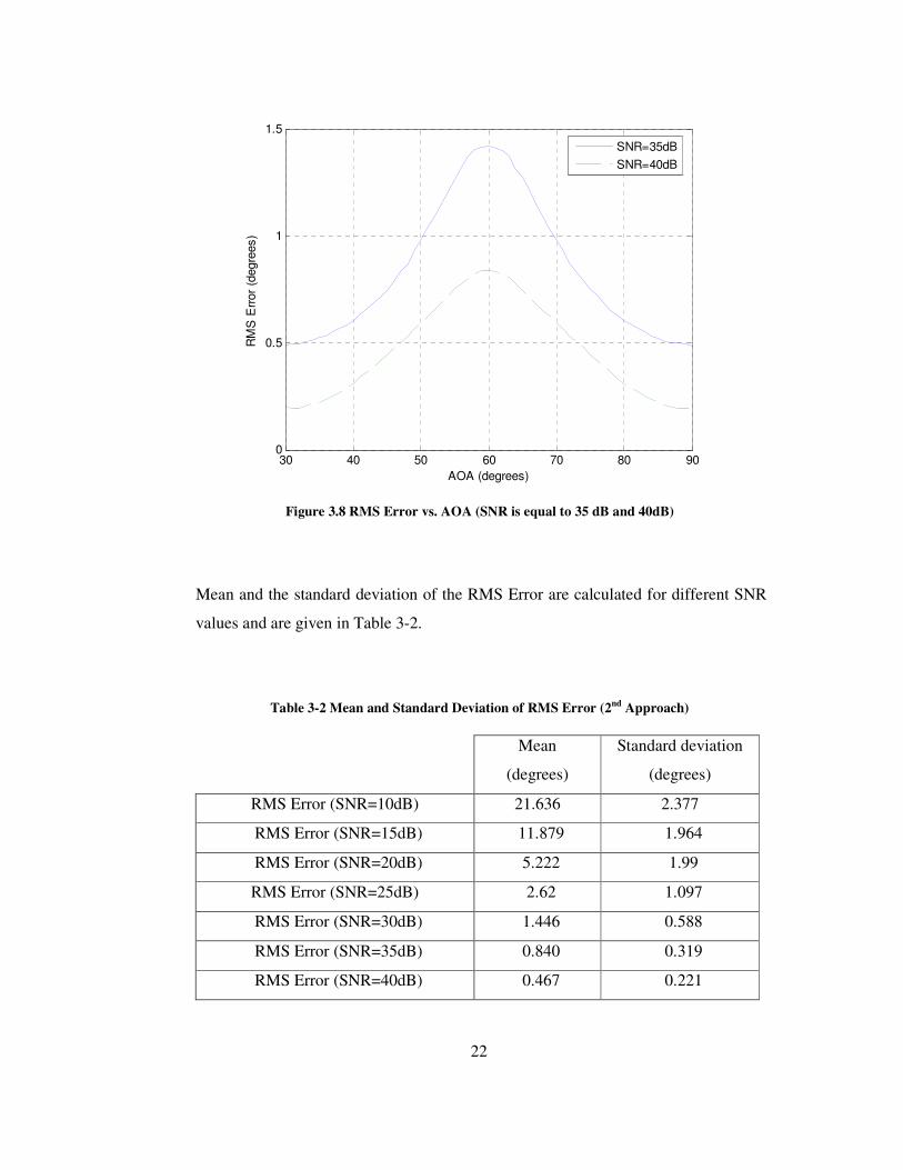
Figure 3.8 RMS Error vs. AOA (SNR is equal to 35 dB and 40dB)
Mean and the standard deviation of the RMS Error are calculated for different SNR
values and are given in Table 3-2.
Table 3-2 Mean and Standard Deviation of RMS Error (2nd Approach)
Mean
(degrees)
Standard deviation
(degrees)
RMS Error (SNR=10dB) 21.636 2.377
RMS Error (SNR=15dB) 11.879 1.964
RMS Error (SNR=20dB) 5.222 1.99
RMS Error (SNR=25dB) 2.62 1.097
RMS Error (SNR=30dB) 1.446 0.588
RMS Error (SNR=35dB) 0.840 0.319
RMS Error (SNR=40dB) 0.467 0.221

23
According to simulation results, even at the same SNR, the RMS error alters along
DOA of the source. It is observed that, for the low SNR cases AOA estimate of the
sources, which are located in the vicinity of direction of the antenna boresight, are
more accurate. The main reason is that the antennas receive high levels of noise
which prevents gathering proper measurement of the pulse amplitude. On the other
hand as SNR increases, AOA estimates of the sources, located in the middle of the
antenna boresights, become more accurate. The reason for this is that SNR is high
and contribution of the other antennas to algorithm makes the DF accuracy better. At
the boresight amplitude fluctuations due to the presence of noise affect the DF
accuracy more, because the antenna gain pattern is linearly stored and is very flat
around the boresight. Therefore, within the beamwidth of the antenna, as AOA gets
further from the boresight, the slope of the antenna gain increases. Consequently
better DF accuracy is obtained.
3.1.1.3 Comparison of Approaches
When two approaches are compared, 2nd approach, which uses pulse amplitudes from
3 antennas, is superior to 1st approach, in which pulse amplitudes from all receiving
channels are used. For low SNR cases DF accuracy of the 2nd approach is better than
the 1st approach. However as SNR value increases both algorithms have
approximately the same DF accuracy. However, considering the overall
performance, the 2nd approach is more preferable; therefore 2nd approach is selected
for the hardware implementation.
Mean of the RMS error is plotted in Figure 3.9 for both approaches.

24
10 15 20 25 30 35 400
5
10
15
20
25
30
35
SNR (dB)
RM
S E
rror
Mean (
degre
es)
1st Approach
2nd Approach
Figure 3.9 Mean of RMS Error vs. SNR
3.1.2 Hardware Implementation
In this part, implementation of the amplitude comparison DF algorithm is
implemented on an FPGA platform by using a commercial software tool, Xilinx
System Generator Tool, is discussed. General information about the software tool
and development tool flow is given in Appendix B.
In the software simulations, floating point double precision values were used to
determine angular location. However, when the algorithm is implemented on FPGA,
fixed point arithmetic is used. As a result the errors due to quantization are
inevitable.
Here the question is how many bits are required for each signal to be represented in
the FPGA. As a general rule for hardware implementation, the number of bits used in
the design is directly proportional to the resources used in FPGA. Therefore the
width of the data should be determined carefully. In the design, actually there are two
signals that data width should be considered carefully; first one is the pulse
amplitude, the other is the antenna gain pattern, which is stored in the RAM.
25
After the signals are received by antennas, they pass through the RF sections and
before processed in FPGA fabric, the IF signals are converted from analog to digital
by ADCs. In today’s technology, throughput of commercial ADC varies from few
MSPS to 12 GSPS [1]. Generally as throughput of the ADC increases, the number of
bits that represent resolution decreases. In today’s technology, ADCs whose
throughput rate is greater than 200 MSPS mostly have 8, 10 or 12 bits for resolution.
Therefore, considering this fact and the process gains in FPGA, it is a good
approximation to determine 12 bits for the pulse amplitude.
The other parameter, whose data width should be determined, is the antenna gain
pattern. Since data width of the received signal pulse amplitude is selected to be 12
bits, the antenna pattern data width should be comparable to data width of pulse
amplitude. Large data widths of antenna gain pattern do not provide much resolution,
since pulse amplitude is already limited to the 12 bits. Consequently, experiments
were performed with 12 bit and 16 bit quantized antenna gain patterns, regarding
different SNR cases.
3.1.2.1 Hardware Design
In the hardware design, inputs to the algorithm are pulse amplitude information from
each receiver channel and a strobe, indicating that the pulse amplitudes are valid and
ready for processing. The output of the hardware implementation is the AOA
estimate of the emitter. Operating frequency is assumed to be constant.
The hardware design is composed of three main blocks. These blocks are;
• AC_Angle_Counter, which filters the necessary pulse amplitudes and
generates a valid search interval.
• AC_Correlation_Computation, which calculates the ML function.
• AC_AOA_Estimator, which estimates the angular location of the emitter.
The purpose and the operational details of each of the implemented block are
presented in the following parts of this chapter. The block diagram of the hardware
implementation is given in Figure 3.10.

26
1
AOA_Est
z -13
Delay_DataReady
z -6
Delay_AOAInterval
PA_Max2
PA_Max
PA_Max3
Addr
Correlation
AC_Function_Calculation
PA_1
PA_2
PA_3
PA_4
PA_5
PA_6
Data_Ready
PA_Max2
PA_Max
PA_Max3
AOA_Interv al_Counter
AC_Angle_Counter
Correlation
AngleIn
Data_Ready
AOA_Est
AC_AOA_Estimator
Sy stem
Generator
7
Data_Ready
6
PA_6
5
PA_5
4
PA_4
3
PA_3
2
PA_2
1
PA_1
UFix_25_24
UFix_10_0 UFix_9_0
UFix_10_0
Bool
double
double
double
double
double
double
UFix_12_12
UFix_12_12
UFix_12_12
double
Figure 3.10 Block Diagram of the Amplitude Comparison Implementation
3.1.2.1.1 AC_Angle_Counter Block
The purpose of this block is to generate a search interval for estimation of AOA. In
monopulse DF systems, not only the DF accuracy but also the process time needed to
determine the AOA is very important. Since the speed of the algorithm is very
crucial, it is better to make calculations in a smaller interval than making calculation
for the entire coverage range.
Implementation of the Angle_Counter consists of three hierarchical blocks.
• AC_Max_PA_Index_Finder, which determines the index of the Antenna
receving maximum pulse amplitude.
• AC_Max_PA_Selector, which selects the proper pulse amplitudes.
• AC_Address_Counter, which generates a valid search interval.
Logic diagram of the AC_Angle_Counter block is given in Figure 3.11.

27
4
AOA_Interval_Counter
3
PA_M ax3
2
PA_Max
1
PA_M ax2
z -4
Delay6
z -4
Delay5
z -4
Delay4
z -4
Delay3
z -4
Delay2
z -4
Delay1
z -3
Delay
Max_Index
PA_1
PA_2
PA_3
PA_4
PA_5
PA_6
PA_Max2
PA_Max
PA_Max3
AC_Max_PA_Selector
PA_1
PA_2
PA_3
PA-_4
PA_5
PA_6
Data_Ready
Index
AC_M ax_PA_Index_Finder
Antenna_No
Data_Ready
AOA_Interv al_Counter
AC_Address_Counter
7
Data_Ready
6
PA_6
5
PA_5
4
PA_4
3
PA_3
2
PA_2
1
PA_1
UFix_3_0
Bool
UFix_12_12
UFix_12_12
UFix_12_12
UFix_12_12
UFix_12_12
UFix_12_12
UFix_10_0
Bool
UFix_12_12
UFix_12_12
UFix_12_12
UFix_12_12
UFix_12_12
UFix_12_12
UFix_12_12
UFix_12_12
UFix_12_12
Figure 3.11 Logic Diagram of AC_Angle_Counter Block
3.1.2.1.1.1 AC_Max_PA_Index_Finder Block
The purpose of this block is to determine the antenna, at which the maximum pulse
amplitude is received. Pulse amplitudes of the received signals are input to this block
and output is the antenna index.
The logic diagram of the AC_Max_Amplitude_Finder block is given in Figure 3.12.

28
1
Index
xlrelational
z-1
a
ba<b
Relational4
xlrelational
z-1
a
ba<b
Relational3
xlrelational
z-1
a
ba<b
Relational2
xlrelational
z-1
a
ba<b
Relational1
xlrelational
z-1
a
ba<b
Relational
xlregisterz-1
d
enq
Register_AOA
xlmux
sel
d0
d1d1
Mux4
xlmux
sel
d0
d1d1
Mux2
xlmux
sel
d0
d1d1
Mux1
xlmux
sel
d0
d1d1
Mux
xl logical
z-1
and
Logical6
xl logical or
Logical5
xl logical and
Logical4
xllogical and
Logical3
xl logical or
Logical2
xl logical
z-1
and
Logical1
xl logical
z-1
and
Logical
xl inv not Inverter5
xl inv not Inverter4
z-4
Delay2
z-1
Delay1
z-1
Delay
xlconcat
hi
lo
cat
Concat
7
Data_Ready
6
In6
5
In5
4
In4
3
In3
2
In2
1
In1Bool
Bool
Bool
UFix_12_12
UFix_12_12
UFix_12_12
Bool
UFix_12_12
UFix_12_12
UFix_12_12
UFix_12_12
UFix_12_12
Bool
UFix_12_12
UFix_12_12
Bool
Bool
UFix_3_0
Bool
Bool
UFix_12_12
Bool
BoolBool
BoolBool
UFix_3_0Bool
Bool
Bool
Figure 3.12 Logic Diagram of AC_Max_Amplitude_Finder Block
3.1.2.1.1.2 AC_Max_PA_Selector Block
The block is designed to determine the maximum pulse amplitude and pulse
amplitudes from antennas which are adjacent to the antenna receiving the maximum
pulse amplitude. The inputs are pulse amplitudes from each receiver channel and the
index of the antenna which received the maximum pulse amplitude. Depending on
the Max_Index input, three pulse amplitudes are filtered. Logic diagram of the
AC_Max_PA_Selector block is given in Figure 3.13.

29
3
PA_Max3
2
PA_M ax
1
PA_Max2
xl relational
z-1
a
ba=b
Relational2
xl relational
z-1
a
ba=b
Relational1
xlm ux
sel
d0
d1d1
M ux4
xlmux
sel
d0
d1d1
M ux3
xlmuxz-1
sel
d0
d1d1
d2
d3
d4
d5
Mux2
xlmuxz-1
sel
d0
d1d1
d2
d3
d4
d5
M ux1
xlmuxz-1
sel
d0
d1d1
d2
d3
d4
d5
M ux
k =5
Constant7
k =0
Constant6
k =0
Constant5
k =5
Constant4k =1
Constant2
k =1
Constant1
xladdsub
z-1a+b
a
b
a
AddSub2
xladdsub
z-1
a-b
a
b
a
AddSub1
7
PA_6
6
PA_5
5
PA_4
4
PA_3
3
PA_2
2
PA_1
1
Max_Index
UFix_3_0
UFix_3_0
UFix_3_0
UFix_12_12
UFix_12_12
UFix_12_12
UFix_12_12
UFix_12_12
UFix_12_12
UFix_12_12
UFix_12_12
UFix_12_12
UFix_1_0
UFix_1_0
UFix_1_0
UFix_3_0
UFix_3_0Bool
UFix_3_0
UFix_1_0Bool
UFix_3_0
Figure 3.13 Logic Diagram of AC_Max_PA_Selector Block

30
3.1.2.1.1.3 AC_Address_Counter Block
The purpose of this block is to generate a sequential search interval for estimating
AOA depending on the antenna, which receives the signal at maximum amplitude.
The determined search interval is 60 degrees around the boresight of this antenna.
The logic diagram of the AC_Address_Counter block is given in Figure 3.14.
1
AOA_Interval_Counter
xl re lational
z-1
a
ba=b
Relationalxl registerz
-1d
rst
en
q
Register
xlmux
sel
d0
d1d1
d2
d3
d4
d5
Mux
z -1
Delay1
out
rst
en
Counter
k =0
Constant7
k =640
Constant6
k =512
Constant5
k =384
Constant4
k =256
Constant3
k =128
Constant2
k =118
Constant1k =1
Constant
xladdsub
z-1a+b
a
b
a
AddSub
2
Data_Ready
1
Antenna_No
Bool
Bool
Bool
Bool
UFix_7_0
UFix_7_0
UFix_1_0
UFix_8_0
UFix_9_0
UFix_9_0
UFix_10_0
UFix_10_0
UFix_10_0
UFix_3_0
UFix_10_0
UFix_10_0
Figure 3.14 Logic Diagram of AC_Address_Counter Block
When Data_Ready strobe is high, the counter value is reset. According to the
Antenna_No input, the beginning of the AOA interval is determined. Then counter
counts up to 120, which is the predetermined search interval. Taking into account the
low SNR cases, this interval should be greater than 60 degrees, 3dB beamwidth. The
center of the search interval depends on the antenna, which receives the greatest
pulse amplitude. The possible search intervals are given in Figure 3.15.

31
Figure 3.15 Search Interval for Amplitude Comparison Implementation
For the high SNR cases, alternatively the search interval can be decreased up to 3 dB
beamwidth of the antenna. This change will result in reduced computation time,
which yields an improvement of total process time for the estimation of AOA.
3.1.2.1.2 AC_Correlation_Computation Block
In order to find the AOA of the incoming signal, as stated in Chapter II, the
algorithm tries to find the argument that maximizes ( )θM in Eq. (2.10). This block
is implemented for calculating ( )θM . It will be useful to rewrite the expression for
( )θM here.
( )( )
( )∑
∑−
=
−
=
−
−
=1
0
2
21
0
N
i
ii
N
i
iii
R
Rs
M
θθ
θθ
θ (2.10)
The logic diagram of the block is given in Figure 3.16.
1
Correlation
xlsl ice[a:b]
Sl ice2
xlsl ice[a:b]
Sl ice1
xlsl ice[a:b]
Sl ice
xlcastforce
Reinterpret3
xlcastforce
Reinterpret2
xlcastforce
Reinterpret1
xl registerz-1
d q
Register2
addr
ROM
xlm ult
z-3
a
b(ab)
M ult2
xlm ult
z-3
a
b(ab)
M ult1
xlm ult
z-3
a
b(ab)
M ult
xladdsub
z-1a+b
a
b
a
AddSub3
xladdsub
z-1a+b
a
b
a
AddSub
4
Addr
3
PA_M ax3
2
PA_Max
1
PA_M ax2
UFix_12_0
UFix_12_0
UFix_12_0
UFix_24_24
UFix_24_24
UFix_12_12
UFix_12_12
UFix_12_12
UFix_10_0
UFix_12_12
UFix_12_12
UFix_12_12
UFix_25_24
UFix_24_24 UFix_24_24
UFix_25_24
UFix_36_0
Figure 3.16 Logic Diagram of the AC_Correlation_Computation Block
32
AC_Correlation_Computation block inputs three pulse amplitudes and the AOA
search interval from previous block. The search interval, Adr, is used for addressing
the ROM block and taking corresponding antenna gain value at the specified angle.
At the hardware implementation phase, a modification is made on the above equation
in order to simplify and eliminate the operation complexity in the hardware. Taking
the square root of both the denominator and the numerator does not affect the
estimated AOA value, since si and Ri are non-negative real values. Moreover,
simplifications will be quite useful for storing the modified antenna gain pattern.
Taking the square root of the Eq. (2-10) yields
( )( )
( )∑
∑−
=
−
=
−
−
=′1
0
2
1
0
N
i
ii
N
i
iii
R
Rs
M
θθ
θθ
θ (3-1)
Antenna pattern is generated at each angle from 1 to 360 degrees at a resolution of 1
degree. At every angle, antenna pattern is normalized and stored. Normalization is
performed according to the following equation.
( ) ( )
( )∑−
=
−
−=′
1
0
2N
i
ii
iii
R
RR
θθ
θθθ
(3-2)
Each memory row in table contains three antenna gains at the same angle. While
forming antenna gain pattern tables, gains are quantized at n bits and merged into 3n
bits wide. Therefore after addressing ROM block, the value received is sliced into
three parts and multiplied with the pulse amplitude values. To calculate ( )θM ′ at the
specified angle, the products are summed up and released as an output of the block.
The overall pipelined latency of this block is 6 clock cycles for each angle value.
Reading table data from the memory is performed in a single clock cycle. In order to
minimize the process time, multiplication and addition of the values are done in
parallel in 5 clock cycles. As a result, the value of the function is ready at the output
of the block for each AOA, after a process delay 6 clock cycles.

33
3.1.2.1.3 AC_AOA_Estimator Block
This block is the final block that estimates the AOA of the incoming signal. The
inputs to this block are the angle within the search interval, value of ( )θM ′ at this
angle and the strobe, indicating that the pulse amplitudes are ready. Output of this
block is the estimated AOA value.
The logic diagram of the block is given in Figure 3.17.
1
AOA_Est
xlsl ice[a:b]
Sl ice_IndexNo
xlsl i ce[a:b]
Sl i ce_AntNo
xlrelationa l
z-1
a
ba>b
Relational
xlrelationala
ba >=b
Relation_MaxFlag
xlregisterz-1
d
rst
en
q
Register_MaxCorr
xlregisterz-1
d
enq
Register_AOA
xlregisterz-1
d
enq
Register
xlmux
sel
d0
d1d1
d2
d3
d4
d5
Mux2
xlmux
sel
d0
d1d1
M ux1
z -121
DelayLine
k =360
Constant7
k =181
Constant6
k =241
Constant5
k =121
Constant4
k =61
Constant3
k =301
Constant2
k =1
Constant1
xladdsub
z-1
a-b
a
b
a
AddSub1
xladdsuba+b
a
b
a
AddSub
3
Data_Ready
2
AngleIn
1
Correla tion
UFix_25_24
Bool
UFix_10_0
UFix_25_24
Bool
UF ix_10_0
Bool
UFix_10_0
UFix_9_0
UFix_1_0
UFix_3_0
UFix_7_0
UFix_6_0
UFix_8_0
UFix_8_0
UFix_9_0
UFix_7_0
UF ix_9_0
UFix_9_0
Bool
UFix_9_0
UFix_9_0
Figure 3.17 Logic Diagram of AC_AOA_Estimator Block
The function of this block is to find the angle, at which maximum of the function
occurs, over the predefined search interval. When a maximum point is found, angle
value corresponding to this point is latched, and at the end of search interval, this
value is presented as an output of the block.
In order to synchronize the Correlation, Angle_In and Data_Ready signals and to
make proper AOA estimate, the signals are delayed by using delay blocks in
previous blocks.

34
After Data_Ready strobe makes a transition to high state, 137 clock cycles later
AOA_Est is ready. The latency is as follows; 7 clock cycles in AC_Angle_Counter
block to determine the search interval, 6 clock cycles to calculate the function ( )θM ′
120 clock cycles to calculate the ML function and 4 clock cycles to find angle, at
which the maximum of the ML function is encountered.
3.1.2.2 Simulation Results
As stated in the hardware implementation part, experiments were performed with 12
bit and 16 bit quantized antenna gain patterns, regarding different SNR cases. (5x10³
Iterations were performed for each AOA value.)
In the hardware design, when performing a multiplication, adjustments are made in
order not to lose the precision at the output. For the 12 bit simulation, the
multiplication of two values, 12 bit unsigned where binary point 12th bit and 16 bit
unsigned where binary point 16th bit, the product is 28 bit unsigned where binary
point in 28th bit. Similar procedure is also applied for 12 bit simulation. In addition,
saturation arithmetic and rounding have area and performance costs [12]. Therefore
they are used only if necessary.
The clock rate of the system is set to 200 MHz, which corresponds to 5 ns of clock
period. While implementing multiplier blocks in FPGA, it is advantageous to use
18x18 dedicated embedded multipliers [11]. This provides flexibility in hardware
design. Since these multipliers are dedicated, no FPGA resources are used. Therefore
the logic, which is planned to be used for multiplication block, can be used for
implementation of other blocks.
The screenshot of the scope from the hardware implementation is given in Figure
3.18. In the simulation, the pulses are generated with pulse repetition interval (PRI)
of 1 µs., where SNR value is set to 30dB and AOA of the emitter is selected to be
250 degrees. In the Figure 3.18, search interval, ( )θM ′ function, Estimated AOA
and Data_Ready signals are plotted for each pulse.

35
Figure 3.18 Screen Shot from System Generator (Implementation of Amplitude Comparison)
Since the antenna patterns are symmetric along the direction of the beam axis, there
exist 6 identical zones in the 360 degree azimuth coverage that have the same
antenna gain pattern. Therefore the experiments are performed in 60 degree interval
at a resolution of 1 degree. RMS Error of the 12 bit and 16 bit hardware
implementation simulations for 20dB SNR and 30 dB SNR are given in Figure 3.19
and Figure 3.20 respectively.
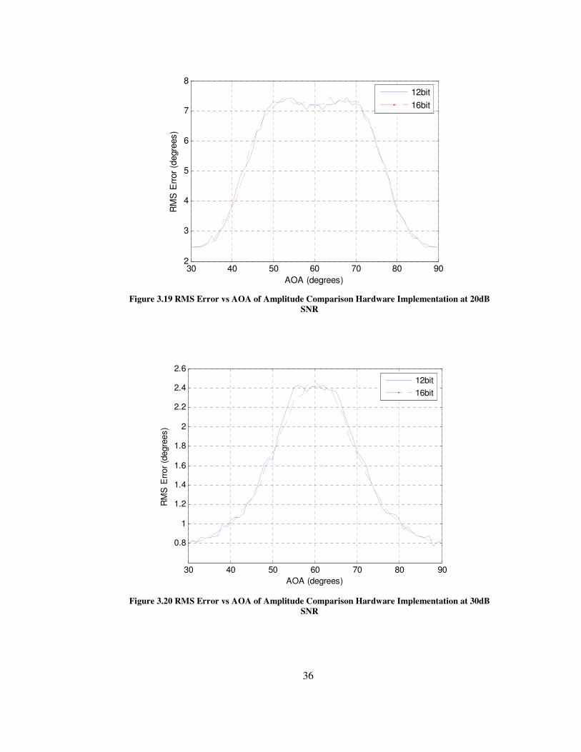
36
30 40 50 60 70 80 902
3
4
5
6
7
8
AOA (degrees)
RM
S E
rror
(degre
es)
12bit
16bit
Figure 3.19 RMS Error vs AOA of Amplitude Comparison Hardware Implementation at 20dB
SNR
30 40 50 60 70 80 90
0.8
1
1.2
1.4
1.6
1.8
2
2.2
2.4
2.6
AOA (degrees)
RM
S E
rror
(degre
es)
12bit
16bit
Figure 3.20 RMS Error vs AOA of Amplitude Comparison Hardware Implementation at 30dB
SNR

37
Mean and standard deviation statistics of RMS Error of the 12 bit and 16 bit
simulation results at 20dB and 30dB SNR are given in Table 3-3.
Table 3-3 Mean and Standard Deviation of RMS Error for Amplitude Comparison Hardware
Implementation
Mean
(degrees)
Standard deviation
(degrees)
RMS Error 12 bit (SNR = 20dB) 5.245 1,976
RMS Error 16 bit (SNR = 20dB) 5.240 1.994
RMS Error 12 bit (SNR = 30dB) 1.467 0.6
RMS Error 16 bit (SNR = 30dB) 1.448 0.58
Table 3-3 summarizes the performance of two hardware implementations having
different number of bits for representing the antenna gain pattern. According to
simulation results, storing the antenna gain pattern table 12 bit precision or 16 bit
precision does not affect the DF accuracy of the algorithm much, since the amplitude
of the signal is limited by 12 bits. But it is observed that In 16 bit implementation
mean of estimated AOA values are more accurate due to greater quantization steps.
When these results are compared to software simulation results, both implementation
results are very close to the results obtained in software simulation. Both 12 bits and
16 bits hardware implementations provide sufficient resolution, since calculated
quantization errors are very small.
For the hardware implementation, the utilization of the FPGA resources is given in
Table 3-4.

38
Table 3-4 FPGA Resource Utilization Summary of Amplitude Comparison Implementation
Number of Slice 396
Number of Slice Flip Flops 467 Number of 4 input LUTs 517
Number of IOBs 83 Number of MULT18X18s 3 Total equivalent gate count for design: 156.176
It is useful to give some information about the timing constraints. According to the
generated clock report of the implementation, following results are obtained.
Requested Constraint : 5.000ns
Actual Constraint : 4.813ns
The number of signals not completely routed for this design is: 0 ns
The average connection delay for this design is 0.827 ns
The maximum pin delay is: 3.029 ns
The average connection delay on the 10 worst nets is: 2.338 ns
Listing Pin Delays by value: (ns)
d < 1.00 < d < 2.00 < d < 3.00 < d < 4.00 < d < 5.00 d >= 5.00
1823 850 61 1 0 0
According to synthesis report all constraints were met and all signals are completely routed.

39
3.2 Phase Comparison
The phase comparison system has two receiver channels following the antennas.
Similar to the amplitude comparison system, the signals received by the antennas
pass through RF paths and are sampled by ADC. After these phases, the digital
signals are directed to FPGA. In the FPGA, it is assumed that Pulse Descriptor Word
(PDW) Generator block measures parameters of the received signals in FPGA and
extract the properties like pulse amplitude, frequency, pulse width etc. Part of this
PDW Generator block supplies pulse amplitude and the frequency information of the
received signal to phase comparison block. The block diagram of the system is given
in Figure 3.21.
Figure 3.21 Block diagram of the Phase Comparison DF system
A single baseline interferometer is assumed in the phase comparison system. As
shown in Figure 3.22, two antennas are located on a straight line with spacing of d.
The antennas are assumed to have the same antenna gain patterns. The phase
difference is measured by two identical antennas in space, separated by a finite
baseline. The phase difference occurs from the extra time it took a plane wave to
travel a greater distance to the further antenna. If the source of the signal is located at
equal distance from the antennas, the phase difference would be zero. In this case, a
phase difference of null arises at the boresight of the antenna.

40
dsin(φ)
X
X
Figure 3.22 Single Baseline Interferometer
The signal received by Antenna 2 can be expressed as
Xjwt
AeS λ
Π−
=2
2 (3-3)
where, A represents initial signal amplitude, X is the distance traveled by the signal
to reach the Antenna 2, λ is the wavelength of the traveling antenna and d is the
distance between the antennas.
In the same manner, signal received by Antenna 1 is given by
( )ϕλ
πsin
2
1
dXjwt
AeS+−
= (3-4)
Where, ϕsind term represents the additional path to Antenna 1 as reference to
Antenna 2. Since the important parameter in this case is phase difference of the
arriving signals, ( )Xλπ /2 can be assumed to be zero. Subtracting the natural
logarithm of the Eq.(3-4) from the natural logarithm of the Eq.(3-3) yields to
ϕλ
πsin
2lnln 12
djSS =− (3-5)

41
Let θ be defined as a phase difference. Therefore θ can be expressed as
ϕλ
πθ sin2d
= (3-6)
As an examination of the above equation, the value of d/λ ratio is very crucial. When
d/λ ratio is equal to 1/2, the phase difference θ is in the interval between 0 andπ .
According to this interval, AOA ϕ has two solutions, which reside in the first
quadrant and in the second quadrant. In the same manner, if d/λ is chosen to be 1, the
phase difference is between 0 and 2π , and like in the previous case, there are two
solutions, since phase difference is not a multiple of 2π . When d/λ ratio is selected
to be n, where n is an integer greater than 1, the phase difference is in the interval
between 0 and 2π n. In this case there are 2n solutions, n of which are in the first
quadrant and the other n solutions reside in the second quadrant.
In the experimental work, AOA of the signals propagating from first quadrant is
assumed to be positive and AOA of the signals from the left side of boresight will be
regarded as negative. Therefore, AOA will be determined in the interval between -90
and 90 degrees, covering the 180 degree range.
Figure 3.23 Phase Comparison Antenna Layout

42
As part of implementation of the phase comparison algorithm, software simulations
are performed. In software simulations antennas are assumed to be omni-directional,
since the phase difference of the received signals is the primary concern. According
to the phase comparison algorithm stated in Chapter II, one of the antenna patterns is
stored as complex valued. In Figure 3.24 real and imaginary parts and in Figure 3.25
phase and gain of the antenna pattern is plotted when λ/d is equal to 2.
-90 -80 -70 -60 -50 -40 -30 -20 -10 0 10 20 30 40 50 60 70 80 90
-1
-0.5
0
0.5
1
Angle (degrees)
real part
imaginary part
Figure 3.24 Real and Imaginary parts of Phase Comparison for d/λ=2

43
-90 -80 -70 -60 -50 -40 -30 -20 -10 0 10 20 30 40 50 60 70 80 90
-1
-0.5
0
0.5
1
Angle (degrees)
phase (pi)
gain (dB)
Figure 3.25 Phase Comparison Antenna Gain and Phase Pattern for d/λ=2
The AOA of the received signals can be estimated by the argument that maximizes
the function ( )φθ ,,AJ . The typical plot of ( )φθ ,,AJ is given in Figure 3.26, where
direction of arrival is set to 35 degrees. The function is plotted for both when
1/ =λd and 5/ =λd .
-90 -80 -70 -60 -50 -40 -30 -20 -10 0 10 20 30 40 50 60 70 80 900
0.5
1
1.5
2
2.5
AOA (degrees)
J (
)
d/Lambda=1
d/Lambda=5
Figure 3.26 Typical Plot of ( )φ'J vs. AOA for 1/ =λd and 5/ =λd (AOA=35)

44
The most important point of this function is that in each quadrant it has more than
one local maximum point for λ/d values greater than 1. These points are possible
AOA of the received signals.
3.2.1 Software Simulation Results
In order to get rid of the ambiguities and determine angular location, prior
information of possible AOA should be present. As declared in [6], due to
ambiguities, phase comparison systems work with another DF system to provide
more accurate results. Therefore a search interval must be stated to find the
maximum point of the function in order to determine the angular location.
Figure 3.27 Search Interval for Phase Comparison
Therefore, a search interval of θinput ± ∆θ is defined, where θinput represents the prior
AOA information provided by another DF system. At the boundary point in the first
quadrant, where θinput + ∆θ is greater than 90 degrees, the interval limit is set to 90
degrees. At the second quadrant, where θinput – ∆θ is smaller than -90, the interval
limit is set to -90 degrees.
The factors that affect the choice of ∆θ are λ/d ratio, the accuracy of phase
comparison system under the defined SNR and the DF accuracy of the system that
provides prior AOA estimate. Main objective is to detect only the maximum point of
the lobe of interest over the search interval for accurate DF sensing. If great λ/d
value and poor DF accuracy of the prior AOA information is considered, the
determined search interval will not be appropriate. If the search interval is
determined to be large, the other lobes, which create ambiguity, may exist in the
search interval. On the other hand if the search interval is determined to be small,

45
the peak of the desired lobe may not be detected. Consequently in both cases it will
lead to errors in the measurement of AOA which is an unwanted situation. Therefore
to determine the search interval, the λ/d value and the DF accuracy of the other
system should be considered and evaluated carefully where the DF accuracy of the
phase comparison system should not be ignored.
To have a better understanding of λ/d ratio and the DF accuracy, some software
simulations are performed. The results of the experiment varying λ/d ratio vs. RMS
error plots at different SNR levels are given in Figure 3.28, Figure 3.29 and Figure
3.30.
-90 -80 -70 -60 -50 -40 -30 -20 -10 0 10 20 30 40 50 60 70 80 900
1
2
3
4
5
6
7
8
9
10
AOA (degrees)
RM
S E
rror
(degre
es)
d/lambda=0.5
d/lambda=1
d/lambda=1.5
d/lambda=2
d/lambda=2.5
d/lambda=3
d/lambda=3.5
d/lambda=4
d/lambda=4.5
d/lambda=5
Figure 3.28 Phase Comparison RMS Error vs. AOA at λ/d value from 1 to 5 in steps of 0.5
(SNR = 10 dB)

46
-90 -80 -70 -60 -50 -40 -30 -20 -10 0 10 20 30 40 50 60 70 80 900
1
2
3
4
5
6
7
8
AOA (degrees)
RM
S E
rror
(degre
es)
d/lambda=0.5
d/lambda=1
d/lambda=1.5
d/lambda=2
d/lambda=2.5
d/lambda=3
d/lambda=3.5
d/lambda=4
d/lambda=4.5
d/lambda=5
Figure 3.29 Phase Comparison RMS Error vs. AOA at λ/d value from 1 to 5 in steps of 0.5
(SNR = 20 dB)
-90 -80 -70 -60 -50 -40 -30 -20 -10 0 10 20 30 40 50 60 70 80 900
0.5
1
1.5
2
2.5
3
3.5
4
4.5
5
AOA (degrees)
RM
S E
rror
(degre
es)
d/lambda=0.5
d/lambda=1
d/lambda=1.5
d/lambda=2
d/lambda=2.5
d/lambda=3
d/lambda=3.5
d/lambda=4
d/lambda=4.5
d/lambda=5
Figure 3.30 Phase Comparison RMS Error vs. AOA at λ/d value from 1 to 5 in steps of 0.5
(SNR = 30 dB)

47
Phase comparison algorithm has different performance characteristics over the AOA.
Better DF accuracy is obtained for the signals arriving around boresight of the
antenna. As the angle between the boresight of the antenna and the propagation
vector of the signal increases, RMS error increases. For AOA greater than 60
degrees, the RMS error curve has very steep increasing characteristics. If more DF
accuracy is required, it is possible to diminish azimuth coverage from 180 degrees to
approximately 120 degrees. In this configuration, to cover a greater azimuthal range,
more than one interferometer systems can be used to operate together.
To understand the overall DF accuracy of the experimental results, the statistical
information, mean of the RMS error as a function of λ/d is plotted in Figure 3.31
for different SNR values.
0.5 1 1.5 2 2.5 3 3.5 4 4.5 50
1
2
3
4
5
6
7
d/lambda
RM
S E
rror
Mean (
degre
es)
SNR=10dB
SNR=20dB
SNR=30dB
Figure 3.31 Mean of RMS Error vs. λ/d Values for SNR=10dB, 20dB and 30dB
As λ/d increases, mean and the standard deviation of the RMS error decreases and
provide a better angular location. For high SNR values, as expected the algorithm
has a better DF accuracy. For 30dB SNR, ignoring both ends of the entire azimuth

48
range where RMS error is large, an RMS accuracy of 1 degree RMS error mean is
reached for the λ/d values greater than 1.
In phase comparison systems, one of the most challenging problems is to determine
the baseline spacing according to the operating frequency band. The DF accuracy is
directly proportional to the ratio of baseline spacing to the wavelength of the signal.
Therefore the baseline spacing is determined upon the specifications and the needs of
the system.
In this study, the operating frequency band is determined to be between 2 GHz and 6
GHz corresponding to a maximum wavelength of 15 cm and minimum wavelength
of 5 cm. Since λ/d value must be greater than ½, the minimum baseline spacing of
the antennas is limited to 7.5 cm.
For different baseline spacing corresponding λ/d intervals are given by
1/2 < λ/d < 3/2, for d1 = 7.5 cm,
1 < λ/d < 3, for d2 = 15 cm,
3/2 < λ/d < 9/2, for d3 = 22.5 cm.
For the simulation, the baseline spacing is chosen to be to 15 cm and the frequency is
varied between 2 GHz and 6 GHz. Here λ/d is varied between one and three
proving a fair DF accuracy, mostly below RMS error of 2 degrees. Software
simulations were performed to compare with the hardware implementation results.
Software simulation results are plotted in Figure 3.32.

49
-90 -80 -70 -60 -50 -40 -30 -20 -10 0 10 20 30 40 50 60 70 80 900
1
2
3
4
5
6
AOA (degrees)
RM
S E
rror
(degre
es)
freq=2GHz
freq=2.5GHz
freq=3GHz
freq=3.5GHz
freq=4GHz
freq=4.5GHz
freq=5GHz
freq=5.5GHz
freq=6GHz
Figure 3.32 RMS Error vs. AOA when Frequency is varied from 2 GHz to 6 GHz in steps of
500MHz at SNR = 20dB.
2 2.5 3 3.5 4 4.5 5 5.5 60.8
1
1.2
1.4
1.6
1.8
2
2.2
Frequency (GHz)
RM
S E
rror M
ean (degre
es)
Figure 3.33 Mean of the RMS Error vs. Frequency at SNR=20dB.
In order to determine the search interval, prior information of AOA provided by
another DF system must be available. In the simulations, the provided AOA is

50
assumed to be accurate, since main purpose is to calculate DF accuracy of the phase
comparison system.
In order to decide the search interval, some cases are investigated. First, poor DF
accuracy is obtained for small d/λ values and for the angles approaching ±90 degrees
(Figure 3.32). To the ends of the entire angle range, the interval length is limited;
therefore it should not be the main consideration. Considering the case when d/λ is
equal to 1, the RMS error is calculated as 3 degrees around 70 degrees at 20dB SNR.
The interval, in which the estimates reside 99.9 percent of probability, is obtained in
reference [10] as (3.291 x 3) degrees. Hence it is good to consider search interval of
10 degrees in software simulations. Secondly, the angle difference of the maximum
of lobes that makes ambiguity must be taken into consideration. When λ/d is equal
to 3, maximum number of lobes are present in the calculated ML function.
According to Eq.(3-6), phase difference is
( ) kk ϕππθ sin.3.212 =−+ , where k=1, 2, 3
The kϕ ’s that are satisfying the above condition are the solutions. Solutions are the
points which create ambiguity in the ML function. The minimized solution set of the
condition is given by
3/1sinsin 12 =− ϕϕ , where -90<ϕ <90
For this case, solutions, minimizing the search interval, are calculated ±9.5941
degrees. Therefore the angle between two lobes makes at least 19.1881 degrees,
which is greater than defined search interval. Therefore for the simulations θinput ± 10
degrees is a valid search interval.
Before proceeding to hardware implementation of the phase comparison algorithm,
another point to investigate is the frequency resolution of the antenna gain patterns
which will be stored in the RAM. Quantization errors due to frequency resolution
must be evaluated to find an appropriate frequency resolution. Storing the antenna
gain patterns dense over defined frequency interval requires much memory, whereas
storing it sparse results in large quantization errors. Therefore, considering this trade-
off, the quantization interval of the frequency should be determined carefully.

51
For frequency resolution of 100 MHz and 50 MHz, corresponding quantization
errors over the entire frequency range are plotted in Figure 3.34 and Figure 3.35
respectively. In this case, the AOA of the source is set to 30 degrees and the
simulation is performed when there is no noise and when SNR is equal to 20 dB.
2 2.5 3 3.5 4 4.5 5 5.5 60
0.2
0.4
0.6
0.8
1
1.2
1.4
Frequency (GHz)
RM
S E
rror
(degre
es)
Noise free
SNR=20dB
Figure 3.34 The RMS Error vs. Frequency when fresolution = 100 MHz (AOA=30 degrees)
2 2.5 3 3.5 4 4.5 5 5.5 60
0.2
0.4
0.6
0.8
1
1.2
1.4
Frequency (GHz)
RM
S E
rror
(degre
es)
Noise free
SNR=20dB
Figure 3.35 The RMS Error vs. Frequency when fresolution = 50 MHz (AOA=30 degrees)
As a result, the smaller the frequency resolution is used, the less quantization errors
are obtained. For frequency resolution of 100 MHz, there exists a quantization error
even at the noise free case. Therefore, frequency resolution of 50 MHz is more
appropriate. However in the implementation it is better to set the resolution to a
number which is a power of 2. In case of performing a division operation with fix
point numbers, which takes more time and more resource, performing a shift

52
operation takes less resource and is faster. Therefore, the experiments are also
performed for frequency resolution of 64MHz.
2 2.5 3 3.5 4 4.5 5 5.5 60
0.2
0.4
0.6
0.8
1
1.2
1.4
Frequency (GHz)
RM
S E
rror
(degre
es)
Noise free
SNR=20dB
Figure 3.36 The RMS Error vs. Frequency when fresolution=64 MHz (AOA=30 degrees)
According to Figure 3.36, the RMS error is smaller than 0.1 degrees for 20dB SNR
and is getting smaller as the frequency is increasing over the entire frequency range.
3.2.2 Hardware Implementation
In this part, implementation of the phase comparison DF algorithm on an FPGA
platform by using a commercial software tool, Xilinx System Generator Tool
(Appendix B) will be presented. After implementation of the phase comparison
algorithm, the part of the PDW Generator, which performs I and Q demodulation and
delivers the complex amplitude to the phase comparison block, is implemented.

53
3.2.2.1 Hardware Design
In hardware implementation of the phase comparison algorithm, the inputs to the
designed core are;
• the real and imaginary parts of the signals from each channel,
• the frequency of the received signals,
• the estimate of the AOA that another DF system provides.
The output of the hardware implementation is the AOA estimate of the emitter.
In the hardware design, the implementation of the phase comparison DF algorithm
consists of 4 main blocks. These blocks are;
• PC_Angle_Counter, which specifies a valid search interval.
• PC_Address_Decoder, which determines the memory address interval
• PC_Function_Calculation, which computes the ML function.
• PC_AOA_Estimator, which estimates the AOA.
The purpose of the each implemented block is presented in the following parts of the
chapter. The block diagram of the hardware implementation is given in Figure 3.37.
1
AOA_Est
dbl fpt
s2_quad2
dbl fpt
s2_inphase2
dbl fpt
s1_quad1
dbl fpt
s1_inphase1
fpt dbl
mag4
dbl fpt
freq
dbl fpt
STR
Address
s1_real
s1_imag
s2_real
s2_imag
Function
PC_Function_Calculation
Data_Ready
AOA_input
Angle_Count
PC_Angle_Counter
Angle_Count
Frequency
Address
PC_Address
Function
Angle_Count
Data_Ready
AOA_Est
PC_AOA_Estimator
z-5
Delay7
z-5
Delay6
z-5
Delay5
z-5
Delay4
z-3
Delay3
z-16
Delay2
z-12
Delay1
dbl fpt
AOASy stem
Generator
7
Data_Ready
6
s2_imaginary
5
s2_real
4
s1_imaginary
3
s1_real
2
AOA_input
1
Frequency
Figure 3.37 Block Diagram of Phase Comparison Implementation

54
3.1.2.1.4 PC_Angle_Counter Block
The purpose of this block is to determine the search interval of the algorithm. The
inputs to this block are Data_Ready and AOA_input signals. Data_Ready signal
gives information that a new data is ready for search interval calculation. AOA_input
is the AOA value, which another DF system provides. The output is the search
interval, Angle_Count, whose center is AOA_input.
In the design, Data_Ready signal is defined to be Boolean. It is assumed that
AOA_input is in the interval between 90 and -90 degrees. It is represented as 8 bit
signed integer. The output Angle_Count will be used for determining the memory
address in the next block. Therefore it varies between 0 and 180 as an 8 bit unsigned
integer.
The logic diagram of the PC_Angle_Counter block is given in Figure 3.38.
1
Angle_Count
k =10
Search_Interval
xl relational
z-1
a
ba<b
Relational2
xlrelational
z-1
a
ba>b
Relational1xl relational
a
ba=b
Relational
xl registerz-1
d
rst
en
q
Register
xlmuxz-1
sel
d0
d1d1
Mux_MinSearchInt
xlmuxz-1
sel
d0
d1d1
Mux_MaxSearchInt
k =0
Min_Lim it
180
Max_Lim it
z -3
Delay2
out
rst
en
Counter
k =90
Constant5
k =1
Constant
xladdsub
z-1a+b
a
b
a
AddSub6
xladdsuba+b
a
b
a
AddSub5
xladdsub
z-1
a-b
a
b
a
AddSub1
xladdsub
z-1a+b
a
b
a
AddSub
2
AOA_input
1
Data_Ready
Bool
Bool
Bool
UFix_8_0
UFix_7_0
UFix_8_0
Fix_9_0
UFix_8_0
Fix_8_0
Bool
UFix_4_0
UFix_8_0
UFix_8_0
UFix_8_0Bool
F ix_9_0
UFix_8_0Bool
Bool
Figure 3.38 Logic Diagram of the PC_Angle_Counter Block
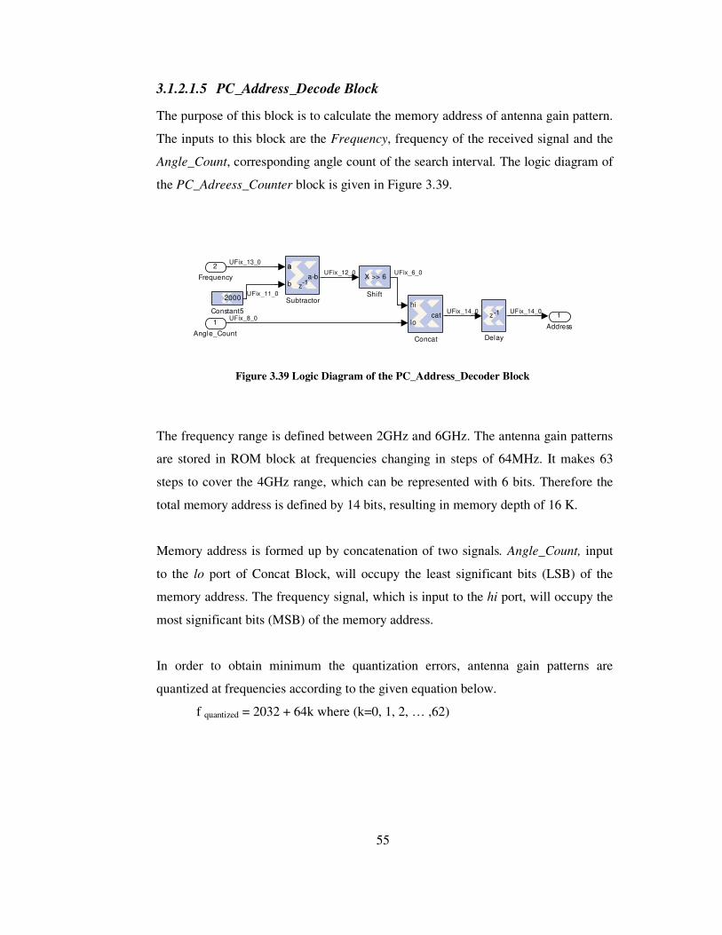
55
3.1.2.1.5 PC_Address_Decode Block
The purpose of this block is to calculate the memory address of antenna gain pattern.
The inputs to this block are the Frequency, frequency of the received signal and the
Angle_Count, corresponding angle count of the search interval. The logic diagram of
the PC_Adreess_Counter block is given in Figure 3.39.
1
Address
xladdsub
z-1
a-b
a
b
a
Subtractor
xlshiftX >> 6
Shift
z-1
Delay
2000
Constant5 xlconcat
hi
locat
Concat
2
Frequency
1
Angle_Count
UFix_13_0
UFix_11_0
UFix_12_0 UFix_6_0
UFix_8_0UFix_14_0 UFix_14_0
Figure 3.39 Logic Diagram of the PC_Address_Decoder Block
The frequency range is defined between 2GHz and 6GHz. The antenna gain patterns
are stored in ROM block at frequencies changing in steps of 64MHz. It makes 63
steps to cover the 4GHz range, which can be represented with 6 bits. Therefore the
total memory address is defined by 14 bits, resulting in memory depth of 16 K.
Memory address is formed up by concatenation of two signals. Angle_Count, input
to the lo port of Concat Block, will occupy the least significant bits (LSB) of the
memory address. The frequency signal, which is input to the hi port, will occupy the
most significant bits (MSB) of the memory address.
In order to obtain minimum the quantization errors, antenna gain patterns are
quantized at frequencies according to the given equation below.
f quantized = 2032 + 64k where (k=0, 1, 2, … ,62)

56
3.1.2.1.6 PC_Function_Calculation Block
The purpose of this block is to calculate the ML function ( )φ/J in Eq.(2-29). The
inputs to the block are the real and imaginary parts of the received signals, s1 and s2,
and the memory address. The logic diagram of the PC_Function_Calculation block
is given in Figure 3.40.
1
Function
xlcastforce
force2
xlcastforce
force1
xlcastforce
ant2_real
xlcastforce
ant2_imag
xlcastforce
ant1_real
xlsl ice[a:b]
Slice3
xlsl ice[a:b]
Slice2
xlsl ice[a:b]
Slice2
xlsl ice[a:b]
Slice1
xlsl ice[a:b]
Slice
addr
ROM xlmult
z-3
a
b(ab)
Mult3
xlmult
z-3
a
b(ab)
Mult1
z-2
Delay6
z-2
Delay5
z-2
Delay4
z-1
Delay3
z-1
Delay2
z-2
Delay11
z-1
Delay1
table_real
table_imag
signal_real
signal_imag
product_real
product_imag
Complex_Multipl ier_2
table_real
signal_real
signal_imag
product_real
product_imag
Complex_Multipl ier_1
xladdsub
z-1a+b
a
b
a
AddSub3
xladdsub
z-1a+b
a
b
a
AddSub1
xladdsub
z-1a+b
a
b
a
AddSub5
s2_imag
4
s2_real
3
s1_imag
2
s1_real
1
Address
UFix_36_0 UFix_12_0
UFix_12_0
UFix_12_11Fix_23_22
Fix_24_22
Fix_23_22
Fix_24_22
Fix_25_22
Fix_25_22
UFix_20_19
UFix_14_0
Fix_12_11
Fix_12_11
UFix_12_0 Fix_12_11
Fix_12_11
Fix_12_11
Fix_12_11
UFix_12_11
Fix_36_34
Fix_36_34
Fix_18_17UFix_18_0
UFix_18_0 Fix_18_17
Fix_12_11
Fix_12_11
Fix_12_11
Fix_12_11
Fix_12_11
Fix_12_11
Figure 3.40 Logic Diagram of PC_Function Calculation Block
In order to find the AOA of the incoming signal, the algorithm tries to find the
argument that maximizes the ratio given in Eq.(2-30), which is rewritten below for
convenience.
( ) ( )
( ) ( )
+
+=
22
2**
||||
dhsgmaxarg
φφ
φφφ
φ hg (2-30)
For the implementation of the algorithm, some simplifications are made on the
equation in order to minimize the number of operations. This will result in faster
process time of the implemented algorithm. Taking the square root of the Eq.(2-30)
does not affect the result of the algorithm. Therefore the algorithm becomes
( ) ( )
( ) ( )
+
+=
22
**
||||
dhsgmaxarg
φφ
φφφ
φ hg
(3-7)

57
Using 64 MHz frequency steps, the antenna gain patterns of two antennas are stored
in the memory. The antenna patterns are defined as
( )( ) ( ) 22
*
||||
g
φφ
φ
hgg
stored +=
(3-8)
( )( ) ( ) 22
*
||||
hh
φφ
φ
hgstored +=
(3-9)
The Eq.(3-7) is simplified in order to find the maximum of storedstored dhsg + function.
As explained in Chapter II, hstored is complex valued; therefore real and imaginary
parts are stored separately. Real and imaginary parts are normalized between 1 and -
1 interval. The other antenna pattern, gstored is purely real; therefore only real part is
stored in memory.
Since the signal and table values are complex valued, two blocks are designed for
performing complex multiplication operation. Then the complex products of the
designed blocks are added together separately as real and imaginary parts. Finally the
magnitude of the products is calculated as an output of the block.
The logic diagrams of the Complex_Multiplier_1 and Complex_Multiplier_2 blocks
are given in Figure 3.41 and Figure 3.42 respectively.
2
product_imag
1
product_real
xlmult
z-3
a
b(ab)
Mult2
xlmult
z-3
a
b(ab)
Mult
z -1
Delay2
z-1
Delay1
3
signal_imag
2
signal_real
1
table_real Fix_12_11
UFix_12_11
Fix_12_11
Fix_23_22 Fix_23_22
Fix_23_22Fix_23_22
Figure 3.41 Logic Diagram of Complex_Multiplier_1 Block

58
2
product_imag
1
product_real
xlmult
z-3
a
b(ab)
Mult3
xlmult
z-3
a
b(ab)
Mult2
xlmult
z-3
a
b(ab)
Mult1
xlmult
z-3
a
b(ab)
Mult
xladdsub
z-1a+b
a
b
a
Adder2
xladdsub
z-1
a-b
a
b
a
Adder1
4
signal_imag
3
signal_real
2
table_imag
1
table_real
Fix_24_22
Fix_24_22
Fix_23_22
Fix_23_22
Fix_23_22
Fix_12_11
Fix_12_11
Fix_12_11
Fix_12_11
Fix_23_22
Figure 3.42 Logic Diagram of Complex_Multiplier_2 Block
3.1.2.1.7 PC_AOA_Estimator Block
The aim of this block is to find the angle at which maximum of the function occurs
over the search interval. The inputs to the block are Data_Ready, Angle_Count and
Function signals. At the end of the search interval, estimated AOA value, AOA_Est,
is presented as an output of the block. The logic diagram of the PC_AOA_Estimator
block is given in Figure 3.43.
1
AOA_Est
xlregisterz-1
d
enq
YonIndex2
xlregisterz-1
d
enq
YonIndex
xlrelationala
ba>b
Relational
xlregisterz-1
d
rst
en
q
Max_Point
z -20
DelayLine k =90
Constant
xladdsuba-b
a
b
a
AddSub
3
Data_Ready
2
Angle_Count
1
Function
Bool
UFix_20_19
UFix_8_0
Bool
UFix_20_19
UFix_8_0
Bool
UFix_8_0
Fix_8_0
UFix_7_0
Figure 3.43 Logic Diagram of the PC_AOA_Estimator Block
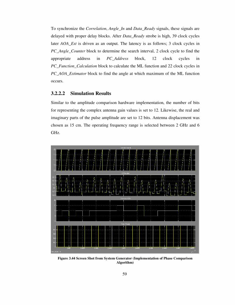
59
To synchronize the Correlation, Angle_In and Data_Ready signals, these signals are
delayed with proper delay blocks. After Data_Ready strobe is high, 39 clock cycles
later AOA_Est is driven as an output. The latency is as follows; 3 clock cycles in
PC_Angle_Counter block to determine the search interval, 2 clock cycle to find the
appropriate address in PC_Address block, 12 clock cycles in
PC_Function_Calculation block to calculate the ML function and 22 clock cycles in
PC_AOA_Estimator block to find the angle at which maximum of the ML function
occurs.
3.2.2.2 Simulation Results
Similar to the amplitude comparison hardware implementation, the number of bits
for representing the complex antenna gain values is set to 12. Likewise, the real and
imaginary parts of the pulse amplitude are set to 12 bits. Antenna displacement was
chosen as 15 cm. The operating frequency range is selected between 2 GHz and 6
GHz.
Figure 3.44 Screen Shot from System Generator (Implementation of Phase Comparison
Algorithm)
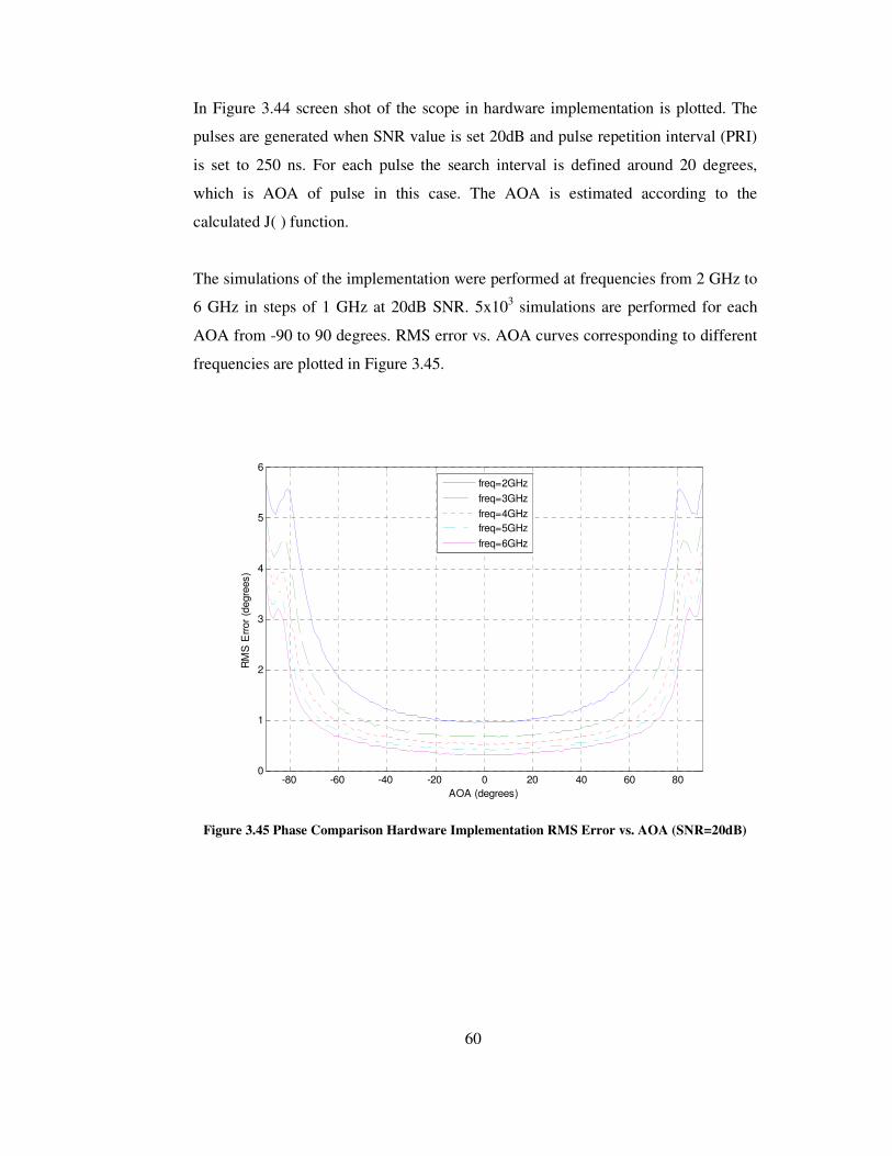
60
In Figure 3.44 screen shot of the scope in hardware implementation is plotted. The
pulses are generated when SNR value is set 20dB and pulse repetition interval (PRI)
is set to 250 ns. For each pulse the search interval is defined around 20 degrees,
which is AOA of pulse in this case. The AOA is estimated according to the
calculated J( ) function.
The simulations of the implementation were performed at frequencies from 2 GHz to
6 GHz in steps of 1 GHz at 20dB SNR. 5x10³ simulations are performed for each
AOA from -90 to 90 degrees. RMS error vs. AOA curves corresponding to different
frequencies are plotted in Figure 3.45.
-80 -60 -40 -20 0 20 40 60 800
1
2
3
4
5
6
AOA (degrees)
RM
S E
rror
(degre
es)
freq=2GHz
freq=3GHz
freq=4GHz
freq=5GHz
freq=6GHz
Figure 3.45 Phase Comparison Hardware Implementation RMS Error vs. AOA (SNR=20dB)
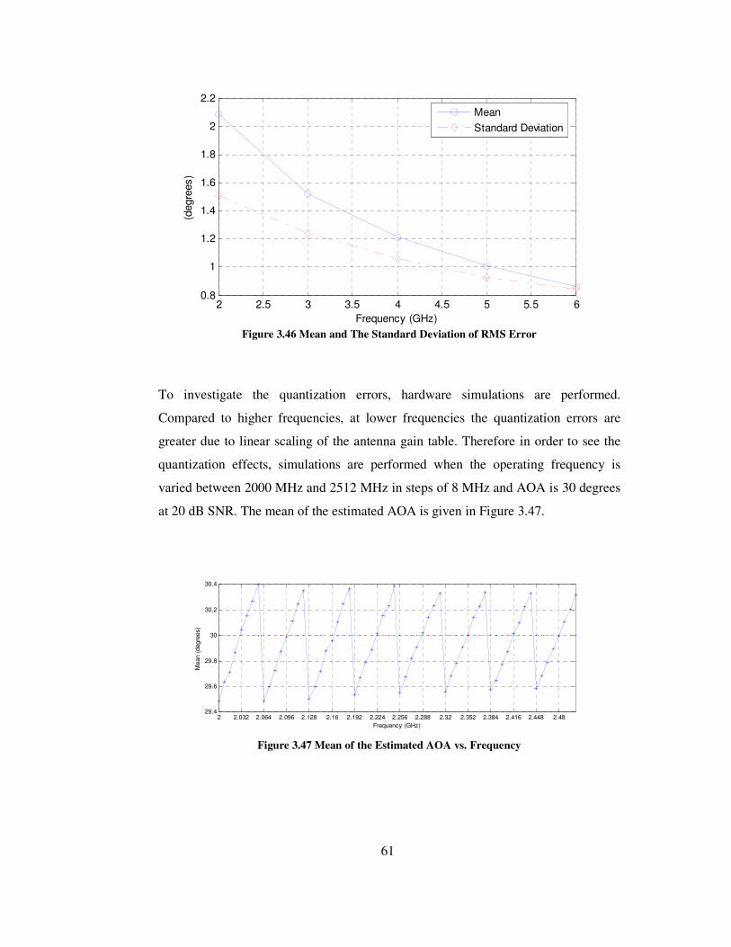
61
2 2.5 3 3.5 4 4.5 5 5.5 60.8
1
1.2
1.4
1.6
1.8
2
2.2
Frequency (GHz)
(degre
es)
Mean
Standard Deviation
Figure 3.46 Mean and The Standard Deviation of RMS Error
To investigate the quantization errors, hardware simulations are performed.
Compared to higher frequencies, at lower frequencies the quantization errors are
greater due to linear scaling of the antenna gain table. Therefore in order to see the
quantization effects, simulations are performed when the operating frequency is
varied between 2000 MHz and 2512 MHz in steps of 8 MHz and AOA is 30 degrees
at 20 dB SNR. The mean of the estimated AOA is given in Figure 3.47.
2 2.032 2.064 2.096 2.128 2.16 2.192 2.224 2.256 2.288 2.32 2.352 2.384 2.416 2.448 2.4829.4
29.6
29.8
30
30.2
30.4
Frequency (GHz)
Mean (
degre
es)
Figure 3.47 Mean of the Estimated AOA vs. Frequency

62
The RMS Error of the hardware implementation due to quantization of frequency is
calculated and is compared with software simulation results in Figure 3.48.
2 2.032 2.064 2.096 2.128 2.16 2.192 2.224 2.256 2.288 2.32 2.352 2.384 2.416 2.448 2.482.5040.85
0.9
0.95
1
1.05
1.1
1.15
1.2
1.25
Frequency (GHz)
RM
S E
rror (d
egre
es)
Software Simulation
Hardware Implementation
Figure 3.48 RMS Error of Hardware Implementation due to Frequency Quantization
The hardware resources, which are utilized for the phase comparison algorithm
implementation, are given in Table 3-5.
Table 3-5 FPGA Resource Utilization Summary of Phase Comparison Implementation
Number of Slices 555 Number of Flip Flops 863 Number of 4 input LUTs 410
Number of External IOBs 78 Number of MULT18X18s 8 Total equivalent gate count for design 2,147,733

63
According to timing analysis, the following results are obtained.
Requested Constraint : 5.000 ns
Actual Constraint : 4.719ns
The number of signals not completely routed for this design is: 0 ns.
The average connection delay for this design is: 0.908 ns.
The maximum pin delay is: 4.079 ns.
The average connection delay on the 10 worst nets is: 3.781 ns.
Listing Pin Delays by value: (ns)
d < 1.00 < d < 2.00 < d < 3.00 < d < 4.00 < d < 5.00 d >= 5.00
2813 1056 169 69 4 0
According to synthesis report, all constraints were met and all signals are completely
routed.
3.2.2.3 Part of PDW Generator Design
After evaluating test results of the hardware implementation of the phase comparison
algorithm, the part of the PDW generator, which extracts the pulse amplitude of the
received signals, is implemented and fitted before the phase comparison algorithm.
In mathematical formulation and implementation, complex valued signals are used.
However in practical usage it is not likely to extract complex representations of each
pulse or continuous wave at the time of sampling. Moreover it is not very usable,
since it is vulnerable to affects of noise or incorrect measurements very much.
Therefore it is more acceptable to represent the received signal per pulse basis or for
CW signals for a period of time.
The hardware implementation consists of three main blocks. These are;
• I_Q_Demodulator, which performs I and Q demodulation.
• Magnitude_Calculator, which calculates the magnitude of the signal.
• Phase_Comparison, which performs phase comparison algorithm.

64
In the simulations the signals are sampled at a rate of 200 MHz. The block diagram
of the hardware implementation is given in Figure 3.49.
fp t dbl
mag4
dbl fpt
freq
simout
To Workspace
0.6
Sl ider
Gain5
0.0424
Slider
Gain4
0.0424
Sl ider
Gain3
0.6
Slider
Gain1
DSP
Sine Wave3
DSP
Sine Wave1
dbl fpt
ST R
Random
Source2
Random
Source1
Pulse
Generator1
Product1
Product
Data_Ready
AOA_input
F req
s1
s2_real
s2_imag
AOA_Est
Phase_Comparison
I_part
Q_part
s1_mag
s2_real
s2_imag
Magni tude_Calcula tor
s ignal_1
s ignal_2
i_part
q_part
I_Q_Demodulator
db l fpt
Gateway In1
dbl fpt
Gateway In
2032
Frequency
Data_Ready
18
AOA_input
db l fpt
AOASy stem
Generator
double
double
double
double double
double
Fix_8_0 double
Fix_8_0
UFix_13_0
double
double
double double
double
double
double
double
double
Fix_12_11
Fix_12_11
Fix_12_11
Fix_12_11
Fix_12_11
Bool
Fix_12_11
Fix_12_11
double
Figure 3.49 Block Diagram of Phase Comparison Implementation
3.2.2.3.5 I_ Q_Demodulator Block
The signals received by the antennas are real valued, and it is assumed that there is
no modulation in the pulse or in the continuous wave. Then the received signals are
defined by
( )wtAs sin1= (3-10)
( )ϕ+= wtAs sin2 (3-11)
where A denotes the pulse amplitude, w is the operating frequency, t represents time
and φ is the phase difference. Demodulation of signals is often done by obtaining in-
phase and quadrature components. There are several methods to decompose the
signal into these components [8]. In this case one of the received signals is used as a
local oscillator. The block diagram of I and Q demodulation process is given Figure
3.50.

65
Figure 3.50 I and Q Demodulation
After the I and Q demodulation is applied, the in-phase and quadrature components
are obtained as
( ) ( ) ( )[ ] ϕϕϕϕ cos2
cos2cos2
1sin.sin.
AwtAwtAwtAI
FilterLP →++=+= (3-12)
( ) ( ) ( ) ( )[ ] ϕϕϕϕ sin2
90cos902cos2
190sin.sin.
AwtAwtAwtAQ
FilterLP →−+−+=−+= (3-13)
According to Eq.(3-12) and Eq.(3-13), after I and Q demodulation process, the
amplitude and phase difference information of original incoming signal is preserved,
whereas frequency is information is lost. The logic diagram of the implementation of
I and Q demodulation is given in Figure 3.51.
2
q_part
1
i_part
xlsl ice[a:b]
Sl ice4
xlsl ice[a:b]
Sl ice3
xlsl ice[a:b]
Sl ice2
xlsl ice[a:b]
Sl ice1
xlsl ice[a:b]
Sl ice
xlcastforce
Reinterpret4
xlcastforce
Reinterpret3
xlcastforce
Reinterpret2
xlcastforce
Reinterpret1
xlcastforce
Reinterpret
xlmul t
z-3
a
b(ab)
Mult1
xlmul t
z-3
a
b(ab)
Mult
xl fi r33 tapxn yn
FIR_LPF2
xl fi r33 tapxn yn
FIR_LPF1
xl fi r33 tapxn yn
FIR_Hi lbertT ransform
xl fi r64 tapxn yn
FIR_Averaging2
xl fi r64 tapxn yn
FIR_Averaging1
FDAT ool
FDAT ool1
FDAT ool
FDAT ool
z -29
Delay1
z -29
Delay
2
signal_2
1
signal_1
Fix_30_26
Fix_12_11
Fix_12_11
Fix_23_22
Fix_23_22
Fix_40_37
Fix_40_37
Fix_37_34
Fix_37_34
Fix_12_11
Fix_12_11
UFix_12_0 Fix_12_11
UFix_12_0 Fix_12_11
UFix_15_0 Fix_15_14
UFix_20_0 Fix_20_19
UFix_20_0 Fix_20_19
Figure 3.51 Logic Diagram of I and Q Demodulator Block

66
In order to lag the second signal by 90 degrees, an FIR filter is designed. The filter
performs a Hilbert Transformation, which is an all pass and performs 90 degree
phase shift. The filter is designed to pass the signals between 10 MHz and 90 MHz.
The magnitude response of the 33 tap filter is shown in Figure 3.52.
Figure 3.52 Magnitude Response of FIR Filter (Hilbert Transformation)
According to Eq. (3-12) and Eq. (3-13), the signals are exposed to a low pass filter
(LPF) to eliminate higher order frequencies. The filter is designed to pass the signal
that has a frequency smaller than 10 MHz. The magnitude of the 33 tap LPF is
shown in Figure 3.53.
Figure 3.53 Magnitude Response of FIR LPF

67
After the signals are filtered through LPF, they are averaged by another FIR filter. In
the implementation the FIR filter has 64 taps with constant coefficients. Alternatively
more or less filter taps can be utilized depending on the pulse width of the received
signal.
3.2.2.3.6 Magnitude_Calculator Block
The inputs to this block are in-phase and quadrature components and the output is the
amplitude of the received signals. For the output, the real part of the signal is
represented by in-phase component; on the other hand the imaginary part is
represented by quadrature component. The other input is accepted as a reference and
only magnitude of the signal is calculated since the phase difference is contained in
the first output. The rearranged signals are given by
21
As =′ (3-14)
ϕϕ sin2
cos22
Aj
As +=′ (3-15)
The logic diagram of the Magnitude_Calculator block is given in Figure 3.54.
3
s2_imag
2
s2_real
1
s1_m ag
xlsl ice[a:b]
Sl ice2
xlsl ice[a:b]
Sl ice1
xlcastforce
Reinterpret2
xlcastforce
Reinterpret1
xlregisterz-1
d
enq
Register2
xlregisterz-1
d
enq
Register1
xlm ul t
z-3
a
b(ab)
M ult2
xlm ul t
z-3
a
b(ab)
M ult1
z -30
Delay2
z -30
Delay1z-200
Delay
1.67651367188
Constant1
k =1
Constant
z -33
x
y
mag
atan
CORDIC AT AN
2
Q_part
1
I_part
Bool
Fix_12_11
Fix_12_11
Bool
F ix_12_11
Fix_12_11
Fix_23_22
Fix_23_22
Fix_12_11
UFix_13_12
UFix_12_0Fix_23_22 Fix_12_11
UFix_12_0Fix_23_22 Fix_12_11
Figure 3.54 Logic Diagram of Magnitude_Calculator Block

68
3.2.2.4 Simulation Results
The output of the PDW generator block is driven to the phase comparison block to
locate the angular position. Since one of the input signals is represented as a pure real
signal, a minor modification is made in the hardware implementation. The imaginary
part of s1, which is 0, is removed. The modified block diagram of the phase
comparison implementation is given in Figure 3.55.
1
AOA_Est
Address
s1
s2_real
s2_imag
Function
PC_Function_Calculation
Data_Ready
AOA_input
Angle_Count
PC_Angle_Counter
Angle_Count
Frequency
Address
PC_Address
Function
Angle_Count
Data_Ready
AOA_Est
PC_AOA_Estimator
z-5
Delay6
z-5
Delay5
z-5
Delay4
z-3
Delay3
z-16
Delay2
z-12
Delay1
6
s2_imag
5
s2_real
4
s1
3
Freq
2
AOA_input
1
Data_Ready
Figure 3.55 Block Diagram of the Phase Comparison Implementation
Several simulations are performed under various conditions to have information
about the DF accuracies of the phase comparison algorithm. In order to see the
affects of i and q demodulation and quantization, simulations are performed once
again. Since adequate simulation results are obtained for the hardware
implementation of phase comparison algorithm, in this part limited simulations will
be performed and compared to previous results.

69
In the simulations, sampling rate is set to 200 MHz and AOA chosen as 20 degrees.
White Gaussian noise, whose variance is equal to 1 and mean is 0, is generated and is
added to signal to obtain a SNR value of 20 dB. Simulation results are given in Table
3-6.
Table 3-6 Mean and Standard Deviation of RMS Error of Estimated AOA
Frequency Mean
(degrees)
Standard Deviation
(degrees)
2032 MHz 20.05 1.176
2992 MHz 20.003 0.876
4016 MHz 20.002 0.530
5040 MHz 19.997 0.451
6000 MHz 20.001 0.458
According to the Table 3-6, the mean of the estimated AOA values are very precise.
On the other hand, the standard deviation of the estimations is slightly larger than the
expected results, which are obtained in Chapter 3.2.3. There exist some reasons
beneath this fact. First, the signals are exposed to filters in I and Q demodulation
phase, where some precision is lost in the process. Secondly, between these steps the
signals are truncated and the number of bits is decreased since they grow up large.
Lastly, while finding the magnitude of the in-phase and quadrature components,
again some precision is lost. In short mostly the error occurs due to quantization. On
the other side in I and Q demodulation process, the outputs are averaged with a 64
tap FIR filter. Clearly, averaging the outputs minimizes the affect of noise.
Regarding these points, the DF accuracy is calculated to be slightly larger than the
hardware implementation results.

70
CHAPTER IV
CONCLUSIONS
In this study, two well-known monopulse direction finding techniques, namely
amplitude comparison and phase comparison algorithms are implemented on an
FPGA platform. In both algorithms mathematical modeling is done using maximum
likelihood approach.
The amplitude comparison system consists of a circular array of six equally spaced
antennas. Two approaches are proposed to locate the angular position of the emitter
using the amplitude comparison algorithm. In the first approach pulse amplitudes
received from all of the antennas are used. Whereas in the second approach, first the
antenna that receives the maximum pulse amplitude is determined; then the pulse
amplitudes received from the antennas, which are adjacent to this antenna, are
determined. These three pulse amplitudes are taken into consideration and used in the
DF algorithm. In both approaches the boresight of the antenna, which receives the
maximum pulse amplitude, is selected to be the center of the search interval of 120
degrees. Over this search interval, AOA is estimated depending on the ML function.
According to simulation results, utilizing only three pulse amplitudes instead of pulse
amplitudes from all channels provides a better DF accuracy at low SNR values. As
the SNR value increases both approaches have similar DF accuracies.
The phase comparison system considered consists of a linear phase array of two
omni directional antennas. One of the most important parameter in a phase
comparison system is the ratio of the antenna baseline spacing to the wavelength of
the received signal, since it is directly related to the number of ambiguous points. In
order to resolve ambiguity problem, the prior information of AOA is input to the
algorithm. This AOA is taken as a center of a search interval. Over this search

71
interval, the ML function depending on complex pulse amplitudes and complex
antenna gains are calculated. Consequently AOA is estimated by examining the ML
function.
The primary aim of the thesis is to evaluate both of the algorithms and to implement
them on an FPGA platform. Target platform is selected to be FPGA, since FPGA is
widely used in DSP and digital communication areas. The advantage of using FPGA
is that highly parallel structures can be employed when compared to DSP chips or
microprocessors. By using parallel structures, throughput can be easily increased
according to design specifications. Therefore the throughput is not limited directly by
the core clock, but limited by the FPGA resources. Hence while implementing the
algorithms, the performance and the resource allocation trade-off must be taken into
consideration.
In implementation phase of the algorithms, some limitations and modifications were
considered to meet the desired results. First, the algorithms were modified and
optimized in order to have a better performance with less complexity and less
hardware resources while not distorting the DF accuracy of the algorithms. The form
of antenna gain tables stored in RAM was modified to avoid the operations like
taking square root, multiplying with a constant or division in FPGA. The operations
like division and taking square-root require more hardware resources and have long
cycles of process time. Therefore the results may contain large quantization errors.
Hence, in the hardware design these operations were avoided as much as possible.
Another important point is the number of bits required for each signal to be
represented in the FPGA. The number of bits used in the design is proportional to the
resources used in FPGA. Number of bits in the algorithm was chosen to be 12 for
representing the signal amplitudes and antenna gain tables. The calculated
quantization errors were very small, since insignificant precision is lost regarding the
FPGA resource allocation.
Hardware simulations of both algorithms were performed at a FPGA clock frequency
of 200 MHz, which is equivalent to 5 ns of clock period. The amplitude comparison
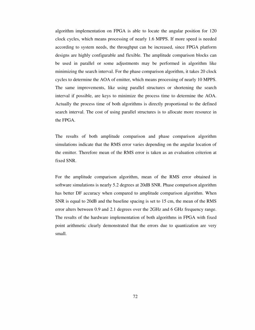
72
algorithm implementation on FPGA is able to locate the angular position for 120
clock cycles, which means processing of nearly 1.6 MPPS. If more speed is needed
according to system needs, the throughput can be increased, since FPGA platform
designs are highly configurable and flexible. The amplitude comparison blocks can
be used in parallel or some adjustments may be performed in algorithm like
minimizing the search interval. For the phase comparison algorithm, it takes 20 clock
cycles to determine the AOA of emitter, which means processing of nearly 10 MPPS.
The same improvements, like using parallel structures or shortening the search
interval if possible, are keys to minimize the process time to determine the AOA.
Actually the process time of both algorithms is directly proportional to the defined
search interval. The cost of using parallel structures is to allocate more resource in
the FPGA.
The results of both amplitude comparison and phase comparison algorithm
simulations indicate that the RMS error varies depending on the angular location of
the emitter. Therefore mean of the RMS error is taken as an evaluation criterion at
fixed SNR.
For the amplitude comparison algorithm, mean of the RMS error obtained in
software simulations is nearly 5.2 degrees at 20dB SNR. Phase comparison algorithm
has better DF accuracy when compared to amplitude comparison algorithm. When
SNR is equal to 20dB and the baseline spacing is set to 15 cm, the mean of the RMS
error alters between 0.9 and 2.1 degrees over the 2GHz and 6 GHz frequency range.
The results of the hardware implementation of both algorithms in FPGA with fixed
point arithmetic clearly demonstrated that the errors due to quantization are very
small.

73
REFERENCES
[1] D. Curtis Schleher, “Electronic Warfare in the Information Age”, Artech House,
1999.
[2] Evrim Anıl Evirgen, “Direction Finding With a Uniform Circular Array Placed
on a Moving Platform”, Ms. Thesis, Middle East Technical University, 2001.
[3] Arzu Tuncay Koç, “Direction finding with a Uniform Circular Array via Single
Snapshot Processing”, Ph.D. Thesis, Middle East Technical University, 1996.
[4] Samuel M. Sherman, “Monopulse Principles and Techniques”, Artech House,
1984.
[5] Avionics Department of the Naval Air Warfare Center Weapons Division
“Electronic Warfare and EW Systems”, 1993.
[6] Stephen E. Lipsky, “Microwave Passive Direction Finding”, Wiley, 1987
[7] Ferhat Arıkan, ”Design of a Monopulse Comparison DF processor Using A
Maximum Likelihood Algorithm”, Ms. Thesis, Middle East Technical University,
1992.
[8] Richard G. Wiley, “Electronic Intelligence: The Analysis of Radar Signals”,
Artect House, 1993.
[9] Charles W. Therrien, “Discrete Random Signals and Statistical Signal
Processing”, Prentice Hall, 1992.
[10] Athanasios Papoulis, “Probability, Random Variables and Stochastic

74
Processes”, McGraw-Hill Inc. 1991.
[11] “Virtex-II Pro Platform FPGA Handbook”,Xilinx Inc, 2002.
[12] “Xilinx System Generator for DSP v6.3 User Guide, A Tutorial Indroduction”,
Xilinx Inc, 2004.
[13] Steve Zack, Suhel Dhanani ,”DSP Co-Processing in FPGAs: Embedding High-
Performance, Low-Cost DSP Functions”, Xilinx Inc, 2004.
[14] J. Hwang, B. Milne, “System Level Tools for DSP in FPGAs”, 2001.
[15] AISN Software, “TableCurve 2D”, 1994.

75
APPENDICES
APPENDIX A
A.1 Antenna Gain Pattern
A software tool is utilized to generate the antenna gain pattern for the amplitude
comparison method. The software tool [15] is capable of displaying the X-Y data
along with the fitted equation, and optionally with confidence and/or prediction
intervals, data references and a fit reference. The graph can be scaled and formatted.
A great variety of output options like full numeric evaluation of the selected
equations are available. The equation list is sorted by tool’s goodness-of-fit sort
criteria and its contents can be filtered to only contain certain types of equations.
The main design criteria considered for the generation of the antenna pattern are 3dB
beamwidth, 10dB beamwidth and minimum gain of the antenna. The half-wave
beamwidth of the antenna is determined to be 60 degrees. 10dB beamwidth is
selected to be 120 degrees; and the minimum gain along the antenna pattern is set to
40dB. According to the design specifications, the antenna pattern is obtained by
fitting a Gaussian curve, which is given by
( )
( ) ( ) 2
2
1
2
1
−−−
−+
+= d
cxe
e
d
cxe
bay
(A-1)
where, a is equal to 9.9x10-05, b is equal to 0.9999, c is equal to 180, d is equal to
28.7382 and e is equal to 0.4218.

76
The generated antenna pattern, which is plotted in logarithmic scale, is given in
Figure A.1.
0 30 60 90 120 150 180 210 240 270 300 330 360-40
-35
-30
-25
-20
-15
-10
-5
0
Angle (degrees)
Ga
in (
dB
)
Figure A.1 Generated Antenna Pattern for Amplitude Comparison

77
APPENDIX B
B.1 FPGA’s
A field programmable gate array (FPGA) is a general-purpose integrated circuit. It is
"programmed" by the designer rather than the device manufacturer. Unlike an
application-specific integrated circuit (ASIC), which can perform a similar function
in an electronic system, an FPGA can be reprogrammed, even after it has been
deployed into a system.
An FPGA provides the user with a two-dimensional array of configurable resources
that are used to implement a wide range of arithmetic and logic functions. These
resources include dedicated 18x18 bit multipliers, dual port memories, lookup tables
(LUTs), registers, tristate buffers, multiplexers, and digital clock managers.
FPGAs are high performance data processing devices. FPGA performance is derived
from the ability they provide to construct highly parallel architectures for processing
data. Compared to a microprocessor or DSP processor, where performance is tied to
the clock rate at which the processor can run, FPGA performance is tied to the
amount of parallelism that can be brought to bear in the algorithms making up a
signal processing system. Currently system frequencies of 100-200 MHz are
commonly used today. A combination of increasingly high system clock rates and
highly distributed memory architecture gives the system designer an ability to exploit
parallelism in DSP applications that operate on data streams. For example, the raw
memory bandwidth of a large FPGA running at a clock rate of 150 MHz can be
hundreds of terabytes per second. [12]
There are wide ranges of DSP applications as digital up/down converters, digital FIR
filters etc that can be implemented only in custom integrated circuits (ICs) or

78
specifically in an FPGA. Advantages of using an FPGA include significantly lower
non-recurring engineering costs than those associated with a custom IC (FPGAs are
commercial off-the-shelf devices), shorter time to market, and the configurability of
an FPGA, which allows a design to be modified, even after deployment in an end
application.
Figure B.1 Virtex Family FPGA Logic Slice
Logic Slice is the fundamental unit of the logic fabric array. It is instructive to take a
closer look at the Virtex family logic slice construction, which is given in Figure B.1.
Each logic slice contains two 4-input lookup tables (LUTs), two configurable D-flip
flops, multiplexers, dedicated carry logic, and gates used for creating slice based
multipliers. Each LUT can implement an arbitrary 4-input Boolean function.
Coupled with dedicated logic for implementing fast carry circuits, the LUTs can also
be used to build fast adder/subtractors and multipliers of essentially any word size. In
addition to implementing Boolean functions, each LUT can also be configured as a
16x1 bit RAM or as a shift register (SRL16). An SRL16 shift register is a

79
synchronously clocked 16x1 bit delay line with a dynamically addressable tap point.
In recent years, field-programmable gate arrays (FPGAs) have become key
components in implementing high performance digital signal processing (DSP)
systems, especially in the areas of digital communications, networking, video, and
imaging. The logic fabric of today's FPGAs consists not only of look-up tables,
registers, multiplexers, distributed and block memory, but also dedicated circuitry for
fast adders, multipliers, and I/O processing (e.g., giga-bit I/O). The memory
bandwidth of a modern FPGA far exceeds that of a microprocessor or DSP processor
running at clock rates two to ten times that of the FPGA. Coupled with a capability
for implementing highly parallel arithmetic architectures, this makes the FPGA
ideally suited for creating high-performance custom data path processors for tasks
such as digital filtering, fast Fourier transforms, and error correcting codes [14].

80
APPENDIX C
C.1 Development Tool Flow
Using MATLAB® and Simulink® from MathWorks, coupled with Xilinx System
Generator™ for DSP, signal processing algorithms can be modeled, simulated, and
verified specific to target hardware platform in the Simulink environment. When the
simulation is run, various signals can be stored as variables in the workspace
providing to make post simulation analysis.
The design flow typically involves the following steps: First hardware model is
developed and verified by the using industry tools. Then, Xilinx System Generator
generates an HDL circuit representation that is bit- and cycle-true meaning that the
behavior is guaranteed to match the functionality seen in the simulation model.
Finally, the Integrated Software environment (ISE) design tools synthesize the design
and produce a bitstream that is used to program the FPGA. The error-prone and time-
consuming phase, which is translating the hardware design into HDL, is
automatically done by the software tool [13].
C.2 Xilinx System Generator
System Generator is a new system level tool built on top of Simulink. It facilitates
DSP design for FPGAs. Simulink provides a convenient high level modeling
environment for DSP systems, and consequently is widely used for algorithm
development and verification. System Generator maintains an abstraction level while
keeping the traditional Simulink blocksets. System Generator automatically
translates designs into hardware implementations. The implementation is faithful in
that the system model and hardware implementation are bit-identical and cycle-
identical at sample times as designed in Simulink. The implementation is made
efficient through the use of Intellectual Property (IP) cores that provide a range of

81
functionality from arithmetic operations to complex DSP algorithms. These cores
have been carefully designed to run at high speed and be area efficient [14].
System Generator provides two main Matlab Simulink simulation libraries, the
"Xilinx Blockset" and "Xilinx Reference Blockset". Each library contains blocks that
are used to construct models in Simulink environment. These blocks provide
arithmetic, logic, memory, and signal processing abstractions suitable for
implementing DSP systems in an FPGA platform. In addition to these simulation
libraries, System Generator provides implementations for each function, and code
generation software for translating subsystems comprised of Xilinx blocks into
hardware descriptions of the system model. The simulation models are bit-accurate
to the hardware description, and at sample rates observable in Simulink, are also
clock cycle accurate to the hardware. Consequently, the detailed hardware behavior
can be understood from the Simulink simulation [12].
A System Generator model is constructed of blocks from the Xilinx blocksets, each
of which contributes to the hardware description created by the code generator. One
of the primary advantages of designing hardware using System Generator is the rich
simulation framework Simulink provides to stimulate, debug, and analyze the
executable model [12].
Each realizable signal which is to be translatable into hardware, must be sampled and
be either a fixed-point or Boolean type. Since System Generator’s goal is to model
realizable digital systems, it does not support modeling of continuous time signals.
Data types and sample rates are propagated through a System Generator model under
normal Simulink propagation rules. This means that any source to a System
Generator subsystem must be sampled and quantized. Signals passing from Simulink
blocks to Xilinx blocks must go through Xilinx gateways, which enforce these
constraints [12].
An output data type of Xilinx blocks can be boolean, unsigned, or signed (two's
complement), with a user-defined numerical precision. Figure C.1 shows a Xilinx
Multiplier that forces outputs to be a 16-bit unsigned value, with 15 fractional bits.

82
Quantization parameter can be truncate or round (unbiased: /- Inf). In the user
defined parameters overflow parameter must be selected one of wrap, saturate or
flag as error.
Figure C.1 Function Block Parameters of a Xilinx Multiplier Block
As seen in Figure C.1, FPGA provides flexibility in defining arbitrary fixed point
arithmetic precision throughout the design and computation. The amount of FPGA
hardware resources are directly related to the data width that is defined throughout
design. Therefore it is wise to request only the data width and precision needed.
Otherwise the FPGA resources are used excessively. This will cost more money, less
circuit speed, and much power dissipation.
System Generator is particularly useful for algorithm exploration, design prototyping
and model analysis. When these are the goals, the tool is used to flesh out an
algorithm in order to get a feel for the design problems that are likely to be faced,

83
and perhaps to estimate the cost and performance of an implementation in hardware.
Work is preparatory, and there is little need to translate the design into hardware. In
this setting, a designer assembles key portions of the design without worrying about
fine points or detailed implementation. Simulink blocks and MATLAB .m code
provide stimuli for simulations, and for analyzing results. Resource estimation gives
a rough idea of the cost of the design in hardware. Experiments using hardware
generation can suggest the hardware speeds that are possible.