implementation of full carbon‑based three‑dimensional
TRANSCRIPT

This document is downloaded from DR‑NTU (https://dr.ntu.edu.sg)Nanyang Technological University, Singapore.
Implementation of full carbon‑basedthree‑dimensional interconnects
Zhu, Ye
2019
Zhu, Y. (2019). Implementation of full carbon‑based three‑dimensional interconnects.Doctoral thesis, Nanyang Technological University, Singapore.
https://hdl.handle.net/10356/137382
https://doi.org/10.32657/10356/137382
This work is licensed under a Creative Commons Attribution‑NonCommercial 4.0International License (CC BY‑NC 4.0).
Downloaded on 12 Dec 2021 22:50:37 SGT

Implementation of Full Carbon-Based
Three-Dimensional Interconnects
ZHU YE
SCHOOL OF ELECTRICAL & ELECTRONIC ENGINEERING
2019

1
Implementation of Full Carbon-Based
Three-Dimensional Interconnects
ZHU YE
School of Electrical & Electronic Engineering
A thesis submitted to the Nanyang Technological University
in partial fulfillment of the requirement for the degree of
Doctor of Philosophy
2019

2
Statement of Originality
I hereby certify that the work embodied in this thesis is the result of original
research, is free of plagiarized materials, and has not been submitted for a
higher degree to any other University or Institution.
[Date Here] [Student’s Signature Here]
. . . . 2020/3/6. . . . . . . . . . . . . . . . . . . . . . . . . . . . . . . . .
Date Zhu Ye

3
Supervisor Declaration Statement
I have reviewed the content and presentation style of this thesis and declare it
is free of plagiarism and of sufficient grammatical clarity to be examined.
To the best of my knowledge, the research and writing are those of the
candidate except as acknowledged in the Author Attribution Statement. I
confirm that the investigations were conducted in accord with the ethics
policies and integrity standards of Nanyang Technological University and
that the research data are presented honestly and without prejudice.
[Date Here]
. . . . 2020/3/6. . . . . . . . . . . . . . . . . . . . . . . . . . . . . . . .
Date Prof. Tan Chuan Seng

4
Authorship Attribution Statement
This thesis contains material from 1 paper published in the following peer-
reviewed journal where I was the first author.
Chapter 6 is published as Ye Zhu, Chong Wei Tan, Shen Lin Chua, Yu Dian
Lim, Boris Vaisband, Beng Kang Tay, Eby G. Friedman, Chuan Seng Tan,
“Assembly Process and Electrical Properties of Top-Transferred Graphene on
Carbon Nanotubes for Carbon-Based Three-Dimensional Interconnects”,
Components Packaging and Manufacturing Technology IEEE Transactions on,
DOI: 10.1109/TCPMT.2019.2940511.
The contributions of the co-authors are as follows:
A/Prof. Chuan Seng Tan and Prof. Beng Kang Tay provided the initial
project direction and A/Prof. Chuan Seng Tan edited the manuscript
drafts.
I prepared the manuscript drafts. The manuscript was revised by Dr.
Chong Wei Tan and Dr. Yu Dian Lim.
I co-designed the study with Dr. Chong Wei Tan and performed all the
laboratory work at the School of Electrical and Electronics Engineering.
I also analyzed the data.
All microscopy, including sample preparation, was conducted by me in
Nanyang Nano Fabrication Centre (N2FC).
Mr. Shen Lin Chua assisted in the fabrication and characterization of
the graphene bridge structure.
Dr. Boris Vaisband and Prof. Eby G. Friedman assisted in the
simulations of CNT/graphene interface.
[Date Here] [Student’s Signature Here]
. . . . 2020/3/6. . . . . . . . . . . . . . . . . . . . . . . . . . . . . . . . .
Date Zhu Ye

5
Acknowledgements
I would like to express my deepest gratitude and respect to my thesis advisor,
Prof. Tan Chuan Seng. He was always generous to help and guided me in every aspect.
He taught me so many things, both knowledge and experiences in researches and even
in daily life. He always encouraged me to try my own ideas and was always patient
when I encountered failures. He always responded to my requests and queries in time
and revised my papers word by word carefully. He truly set an example as the
excellent researcher and mentor for me.
I wish to give my sincere thanks to Prof. Tay Beng Kang and Dr. Tan Chong
Wei. As the collaborators of this project, they provided us with all the facilities for
CNT growth and femtosecond laser annealing and meantime the important and
insightful advices. This work would not be possible without their supports.
I wish to give my special thanks to Dr. Lim Yu Dian who helped to revise my
paper and thesis. He also shared his expertise to my research work and kindly offered
great advices for academic writing and presentation.
I appreciate the help from all my friends and colleagues at Nanyang
Technological University. Special thanks are given to Mr. Chua Shen Lin, who taught
and assisted me for the operation of lithography, I-V characterization and wafer
bonding systems and also gave me useful suggestions on my work. Dr. Lin Ye was
senior in the group and we usually had many interesting discussions which greatly
broadened my knowledge in microelectronics especially in the TSV topic. More
thanks are to Dr. Maurice Ange for his assistance in setting up the femtosecond laser
system for the annealing experiments.
I would like to thank the support and resources from Centre for Micro-/Nano-
electronics (NOVITAS), CNRS International NTU THALES Research Alliance

6
(CINTRA) and Silicon Technologies Center of Excellence (Si-COE) at NTU. More
thanks are given to the support from management and staff in Nanyang Nano
Fabrication Centre (N2FC) at NTU.
I would like to thank my families. My parents have sacrificed so much of their
own for nurturing me and giving me the best education. They have always been my
greatest supports.
Finally, I would like to thank all the people I met and all the things I went
through during the most precious and splendid four years of my life, as all the loves
and pains made me grow up mature. Four years of researches brought me more than
just a degree. I learned how to overcome the difficulties with courage and persistence
which will become the spirit leading my life in the future.

7
Table of Contents
Statement of Originality ................................................................................................... 2
Supervisor Declaration Statement .................................................................................... 3
Authorship Attribution Statement .................................................................................... 4
Acknowledgements ......................................................................................................... 5
Table of Contents ............................................................................................................ 7
Abstract ........................................................................................................................... 9
List of Figures ............................................................................................................... 11
List of Tables ................................................................................................................ 15
Chapter 1 : Introduction ................................................................................................ 16
1.1 Background ........................................................................................................ 16
1.1.1 Opportunities and Challenges in Next Generation Integrated Circuits ........ 16
1.1.2 Interconnect Bottleneck ................................................................................ 19
1.1.3 Three-dimensional (3-D) Integrated Circuits (ICs) ...................................... 22
1.2 Motivation .......................................................................................................... 25
1.2.1 Challenges of Flip Chip Bumping and Through Silicon Via (TSV)
Technology ............................................................................................................ 25
1.2.2 Advantages of Carbon Nanomaterials .......................................................... 29
1.2.3 Full Carbon-Based Interconnects ................................................................. 30
1.3 Objective ............................................................................................................ 35
1.4 Major Contributions of Thesis ......................................................................... 36
1.5 Organization of Thesis ...................................................................................... 37
Chapter 2 : A Review of Carbon Nanotubes (CNTs) for Through Silicon Via (TSV)
Interconnects ................................................................................................................. 38
2.1 Through Silicon Vias (TSVs) ............................................................................ 38
2.2 Growth and Fabrication of CNT TSVs ........................................................... 42
2.3 Contact Resistance between CNT and Metal ................................................. 44
2.4 Fabrication of Graphene-CNT Heterostructure ............................................ 45
2.5 Annealing Methods for Metal-CNT Fusion .................................................... 46
Chapter 3 : Free-Standing CNT Growth on the Graphene ........................................... 49
3.1 Introduction ....................................................................................................... 49
3.2 Experimental Objective and Scope .................................................................. 49
3.3 CNT Growth Method ........................................................................................ 50
3.4 Effects of Temperature Profile and Fe Catalyst Thickness .......................... 52
3.5 Growth of Patterned CNT Pillars on the Graphene ...................................... 55

8
3.6 Summary ............................................................................................................ 58
Chapter 4 : CNT Growth within TSVs on the Bottom Graphene Electrodes ............... 59
4.1 Introduction ....................................................................................................... 59
4.2 Experimental Objective and Scope .................................................................. 59
4.3 Designed Fabrication Process Flow ................................................................. 60
4.4 Top-wafer Process: TSV holes Fabrication .................................................... 61
4.5 Bottom-wafer Process: Graphene Patterning and Catalyst Deposition ....... 62
4.6 Die-to-Die Wafer Bonding and Exposure of TSV holes ................................ 67
4.7 CNT Growth within TSVs ................................................................................ 69
4.8 Summary ............................................................................................................ 71
Chapter 5 : Process Exploration of Transferring a Top-Graphene Layer onto CNTs .. 72
5.1 Introduction ....................................................................................................... 72
5.2 Experimental Objective and Scope .................................................................. 72
5.3 Design and Fabrication of the Test Structures for Electrical Study ............ 73
5.4 Transferring Methods of Graphene Layer ..................................................... 76
5.5 Results and Discussion ...................................................................................... 79
5.6 Summary ............................................................................................................ 88
Chapter 6 : Electrical Properties of Direct Graphene-to-CNT Contact ........................ 89
6.1 Introduction ....................................................................................................... 89
6.2 Experimental Objective and Scope .................................................................. 89
6.3 Design and Fabrication of the Graphene Bridge Structure .......................... 89
6.4 Electrical Characterization Method ................................................................ 91
6.5 Results and Discussion ...................................................................................... 92
6.6 Summary .......................................................................................................... 104
Chapter 7 : Femtosecond Laser Annealing for Graphene-CNT Fusion ..................... 105
7.1 Introduction ..................................................................................................... 105
7.2 Experimental Objective and Scope ................................................................ 105
7.3 Femtosecond Laser Power Tuning ................................................................ 105
7.4 Results and Discussion .................................................................................... 108
7.5 Summary .......................................................................................................... 110
Chapter 8 : Conclusion and Future Work ................................................................... 111
8.1 Conclusion ........................................................................................................ 111
8.2 Future Work .................................................................................................... 113
Author’s Publication ................................................................................................... 117
References ................................................................................................................... 118

9
Abstract
Attributing to its outstanding electrical properties and compatibility with
modern electronic devices, there have been numerous studies reported on the
fabrication and characterization of carbon nanotube (CNT)-graphene heterostructure.
Although there have been some efforts toward the application of CNT-graphene
heterostructure for interconnects, none of them demonstrated a full carbon-based
implementation in the through silicon vias (TSVs) for three-dimensional integrated
circuits (3-D ICs). In this study, the development and optimization of CNT-graphene
heterostructure for its application in TSV interconnects were reported. Carbon
nanotubes (CNTs) were firstly free-standing grown on the graphene with thermal
chemical vapor deposition (TCVD) technique, yielding sufficient length (~334μm) and
density (estimated as ~1011 cm-2) which fulfilled the TSV application requirement.
Subsequently, the growth of CNTs within TSVs on the bottom graphene electrodes
was successfully demonstrated. The fabrication processes of top wafer with TSVs of
various diameters (5-50μm) and bottom wafer with patterned graphene electrodes and
catalyst deposition were successfully developed. Next, top TSV wafer and bottom
graphene wafer were bonded and manually ground, followed by wet and dry etching to
completely remove the handling wafer and buried oxide to expose the underlying TSV
holes. By using the same TCVD technique, successful growth of CNTs within the
fabricated TSVs on top of the graphene electrodes was achieved.
In order to complete the full-carbon 3-D interconnection, assembly process of
top graphene layer after CNT growth needs to be further explored. In this work,
transfer process of a top graphene layer onto the as-grown CNT bundles was
successfully performed with direct graphene-to-CNT contact at the interface. The
electrical properties of CNT/graphene contact were characterized by four-point-probe

10
(4PP) I-V measurements of the graphene bridge structure. The results suggested that
an ohmic contact was achieved between the graphene and CNTs. Low CNT bump
resistance of 2.1Ω for 90,000 µm2 CNT area including the CNT/graphene contact
resistance was obtained, demonstrating reduction of contact resistance between CNT
and Au under the same fabrication and measurement conditions.
The conditions of femtosecond laser annealing for the fusion of graphene and
CNTs were explored in this work as well. After the laser power tuning, 0.0166W was
selected as the optimized value for annealing. Laser line scanning was applied at the
graphene/CNT interface and the electrical properties of the pristine graphene bridge
and annealed graphene bridge samples were characterized. The total resistance of the
bridge structure dropped to its lowest (27.3 Ω) after the first laser scanning and
increased after the second and third laser annealing. However, the obtained outcomes
give insufficient evidences to conclude that the resistance dropping was due to the
fusion of graphene and CNTs by the laser annealing. Further studies are needed to
verify the formation of CNT-graphene bonding and its impact on the overall resistance
upon laser annealing.

11
List of Figures
Figure 1.1 Annual sales of US semiconductor firms by technology type [2]. Figure
source: Khan et al., Nature Electronics. Reprinted with permission from [2], © 2018
Springer Nature Publishing AG. ................................................................................... 17
Figure 1.2 “More-Moore” and “More-than-Moore” concepts describing the scaling
trends [13]. Figure source: “More-than-Moore” White Paper, International Technology
Roadmap for Semiconductors (ITRS), 2010. ............................................................... 19
Figure 1.3 A scaling effect on RC delay in interconnects. Figure source: Ryu, Suk-
Kyu’s Ph.D. dissertation [17]. ...................................................................................... 21
Figure 1.4 Schematic diagrams showing the difference between 2-D and 3-D
interconnects (Source: Beyne [27] ): (a) 2-D SiP integration; (b) SoC integration; (c)
3-D integration. Reprinted with permission from [27], © 2006 IEEE. ........................ 24
Figure 1.5 Replace the long global wire in the 2-D scheme by 3-D IC with vertical
connections and shorter wires. Figure courtesy of Kuan-Neng Chen at National Chiao
Tung University, Taiwan. ............................................................................................. 25
Figure 1.6 Reliability problems in TSV structures [43]: (a) Interfacial delamination; (b)
Silicon cracking; (c) Via extrusion (Pop-up). Figure is from online web source: Cho, S.
[43]. ............................................................................................................................... 27
Figure 1.7 Illustrations of layouts with small versus large KOZ around TSVs [44].
Yellow squares are TSV landing pads. Reprinted with permission from [44], © 2010
IEEE. ............................................................................................................................. 28
Figure 1.8 Pillared CNT-graphene nanostructure with 3D network [72]. Reprinted with
permission from [72], © 2008 American Chemical Society. ....................................... 31
Figure 1.9 (a) Scheme and SEM results for the synthesis of SWCNTs directly from
graphene and (b) I–V measurements [84]. Reprinted with permission from [84], ©
2012 Macmillan Publishers Limited. ............................................................................ 33
Figure 1.10 TEM and STEM images of CNT–graphene junctions [84]. Reprinted with
permission from [84],© 2012 Macmillan Publishers Limited. ..................................... 34
Figure 1.11 SEM images of (a) synthesized graphene/CNT composite and (b) TEM
images around the connection between graphene and CNTs [85]. Reprinted with
permission from [85], © 2008 The Japan Society of Applied Physics. ........................ 35
Figure 2.1: 3-D integration using TSV structures: (a) Illustration of TSVs. Figure
courtesy of Chuan Seng Tan at Nanyang Technological University, Singapore. (b)
TSV samples. Figure is from online web source: Ron Maltiel [88] . .......................... 38
Figure 2.2 Processing issues: (a) scallops at sidewall, where TEOS is an insulating
liner material [92]; (b) voids inside TSV [94]; (c) wafer warpage [98]. Reprinted with
permission from [92] [94] [98] , © 2008, 2010 IEEE. ................................................. 40
Figure 2.3 Via-middle process for TSV structures. Figure is from online web source:
Yannou, J. [101] ............................................................................................................ 41
Figure 2.4 Via-last process for TSV structures. Figure is from online web source:
Yannou, J. [101] . .......................................................................................................... 42
Figure 2.5 SEM images of CNT forest on top of the TSV pattern: Fe-catalyst
placement is done by sputtering on Al2O3 layer using (a) 1 nm, (b) 2 nm and (c) 3 nm
Fe [102]. © 2013 IOP Publishing Ltd. .......................................................................... 43
Figure 2.6 SEM images of CNT bundles grown inside the TSV vias with Al2O3 and an
evaporated thin film of (a) 2 nm, (b) 3 nm, (c) and 4 nm Fe, with in (d) a zoom-in of
the 2 nm Fe result [102]. © 2013 IOP Publishing Ltd. ................................................. 43
Figure 2.7 SEM images after dip-coating in 0.1 M FeCl2 (in ethanol) on Al2O3 and

12
CNT growth (a), (b) in individual vias; (c) high-resolution image of a CNT bundle; (d)
TEM image of a typical CNT removed from a TSV [102]. © 2013 IOP Publishing Ltd.
...................................................................................................................................... 44
Figure 2.8 (a) Schematic illustration of the method for fabricating nanotube/carbide
heterostructure by solid-solid reaction (M=Metal) [119]. © 1999 AAAS. (b) TEM and
High-resolution TEM images of the interface between TiC and SWCNT bundle [119].
© 1999 AAAS. .............................................................................................................. 48
Figure 3.1 Photograph of Aixtron Black Magic CVD system (left). The various growth
modes and CNTs types available using Aixtron Black Magic system (right). ............. 50
Figure 3.2 Temperature profile of a typical TCVD growth cycle. The growth time can
vary from 1 to 5 min. .................................................................................................... 52
Figure 3.3 Raman spectra images of CNT growth using three different recipes with
1.1/2.2nm Fe as catalyst. ............................................................................................... 54
Figure 3.4 SEM images of CNTs grown on 2nm Fe with the same growth time (2 min)
under (a) 550 ˚C, (b) 600 ˚C and (c) 700 ˚C. ................................................................ 55
Figure 3.5 SEM images of patterned CNT pillars grown on the graphene layer.......... 57
Figure 3.6 Transmission electron microscopy (TEM) images of the as-grown CNTs. 57
Figure 3.7 Raman spectra images of (a) as-grown CNTs and (b) graphene before/after
CNT growth. ................................................................................................................. 58
Figure 4.1 Schematic illustration of the fabrication process flow of CNT growth within
TSVs on the bottom graphene electrodes. .................................................................... 61
Figure 4.2 SEM images of the cross-section of TSVs with (a) 5, (b) 15 and (c) 50μm
diameters (depths are all 20μm). ................................................................................... 62
Figure 4.3 Optical images (with 5x, 20x and 50x magnification) after graphene
patterning and catalyst deposition: long strips are patterned graphene electrodes and
round circles are deposited catalyst/barrier layers. ....................................................... 64
Figure 4.4 Raman spectra images of the graphene before and after lithography process.
...................................................................................................................................... 64
Figure 4.5 Raman spectra images of graphene before UVO treatment, after 3min and
after 6 min UVO treatment. .......................................................................................... 65
Figure 4.6 AFM topography images (top-row 3D and bottom-row 2D) of 10μm x
10μm area of a) pristine graphene, b) graphene after lithography and c) graphene after
lithography following a 3min UVO treatment. ............................................................. 66
Figure 4.7 Optical images after the handling wafer removal: TSV holes (a) at the
perimeter area and (b) in the middle portion of the die; (c) photo of a real sample after
the grinding and KOH etching process. ........................................................................ 68
Figure 4.8 Optical images after the handling wafer and buried oxide removal: exposed
TSVs at (a) top left, (b) top right, (c) bottom left and (d) bottom right region of the die.
...................................................................................................................................... 69
Figure 4.9 SEM images for CNT growth within TSV: (a) 3 out of 6 via holes have
CNTs grown but none was completely filled by CNTs; (b) a shift of top die leading to
the partially filling of CNTs in the via, inserted figure is a Raman image of CNTs as-
grown; the scattered CNT grown on (c) sidewall and (d) top surface of TSV. ............ 70
Figure 5.1 (a)-(g) Fabrication process flow of the single-side step structure and (h) a
top-graphene layer transferred on CNTs after CNT growth. ........................................ 73
Figure 5.2 SEM images of the samples after CNT growth with the steps etched by (a)
KOH wet etching and (b) DRIE.................................................................................... 74

13
Figure 5.3 (a)-(g) Fabrication process flow of the double-side step structure and (h) a
top-graphene layer transferred on CNTs after CNT growth. ........................................ 75
Figure 5.4 Top-view and side-view illustrations of the bridge structure (a) before and
(b) after graphene transfer with the thermal tape. ......................................................... 76
Figure 5.5 (a) Optical and (b) Raman images of the “float graphene”
(PMMA/graphene layer). .............................................................................................. 77
Figure 5.6 Optical and SEM images after three different graphene transfer processes:
(a) direct dry transfer, (b) dry transfer with a thermal tape and (c) wet transfer in the
DI water. ....................................................................................................................... 79
Figure 5.7 SEM images of the single-side step structure (a) before and (b) after
graphene direct dry transfer; (c) illustrations and (d) results of 2PP I-V measurements
between Au electrodes on the lower side and the higher side of the step before and
after graphene transfer. ................................................................................................. 81
Figure 5.8 (a) Sidewall shortage in the single-side step structure and (b) SEM images
of the sidewall > 90˚ with rough surface ...................................................................... 82
Figure 5.9 (a) Tilted-view and (b) side-view SEM images of the double-side step
structure after CNT growth ........................................................................................... 84
Figure 5.10 Optical image of the double-side step structure after graphene dry transfer
with the thermal tape on to the CNTs ........................................................................... 84
Figure 5.11 (a) Illustrations and (b) results of 4PP I-V measurements of the double-
side step structure before and after the graphene transfer. ............................................ 85
Figure 5.12 SEM images of the bridge structure (a) before and (b) after graphene dry
transfer with the thermal tape. ...................................................................................... 86
Figure 5.13 Optical image of the bridge structure after the graphene layer transferred
and pressed down on to the CNTs. ............................................................................... 87
Figure 5.14 (a) Illustrations and (b) results of 4PP I-V measurements of the bridge
structure before and after the graphene transfer. .......................................................... 87
Figure 6.1 Fabrication and assembly steps of the Au-CNT-graphene-CNT-Au structure.
...................................................................................................................................... 90
Figure 6.2 (a) Optical and (b) Raman images of the graphene on SiO2/Si and PET. ... 93
Figure 6.3 Schematic diagrams and SEM images of two configurations of CNT area
with the same size (left: configuration A, right: configuration B). ............................... 94
Figure 6.4 (a) and (b) SEM images after CNT growth; (c) and (d) optical images after
top graphene layer transferred; (e) and (f) SEM cross-section view of two CNT walls
of the dummy sample cut in half. ................................................................................. 95
Figure 6.5 (a) Cross-section SEM image of the vertical length of CNT walls on the
dummy sample and (b) the planar length of CNT walls on the same dummy sample
from the top-view SEM image tilted at 20˚. ................................................................. 96
Figure 6.6 The planar length of CNT walls on the real sample from the top-view SEM
image tilted at 20˚. ........................................................................................................ 96
Figure 6.7 (a) Raman and (b) transmission electron microscopy (TEM) images of the
as-grown CNTs. ............................................................................................................ 97
Figure 6.8 4pp I-V measurement results of the total resistance of the graphene and Au
bridge structure with two configurations of CNT area. ................................................ 98
Figure 6.9 SEM images of cross-section view of the graphene bridge structure
(SiO2/Si substrate) with CNT area in configuration B. ................................................ 99
Figure 6.10 Illustration of two Cu electrodes replacing the two CNT bundles on the
top of Au film. ............................................................................................................ 100
Figure 6.11 Optical images of patterned two Cu electrodes on the Au film with three

14
different values of L_Cu ............................................................................................. 101
Figure 6.12 The linear response of the total resistance vs. L_Cu. .............................. 101
Figure 7.1 (a) Illustration of the laser beam focus position on the graphene/CNT
interface and (b) The burn marks of laser power tuning results. ................................ 107
Figure 7.2 Illustration of 3 laser line scans covered the full length of one CNT wall.
.................................................................................................................................... 109
Figure 7.3 Comparison of the I-V curves before and after 1st laser annealing. ......... 109
Figure 7.4 Comparison of (a) the graphene bridge sample through the laser annealing
and (b) graphene-on-CNT sample (discussed in Chapter 6). ...................................... 110

15
List of Tables
Table 1.1 Typical physical properties of Si, Cu and CNT at room temperature [70]. .. 30
Table 3.1 Recipe tuning for MWCNT growth .............................................................. 54
Table 3.2 Density and length of CNT growth with the same growth time (2 min) under
different temperature (550, 600 and 700 ˚C). ............................................................... 54
Table 4.1 Ar plasma and UV-ozone treatment for graphene samples. ......................... 65
Table 6.1 The vertical and planar length of CNT walls on the dummy sample and real
sample. .......................................................................................................................... 96
Table 6.2 4PP I-V measured total resistances of different L_Cu from three batches of
samples. ....................................................................................................................... 101
Table 6.3 Total and extracted one CNT bump resistance of the graphene and Au bridge
structure with two configurations of CNT area. ......................................................... 102
Table 6.4 Resistance of one CNT bump (including the CNT/metal (CNT/graphene)
contact resistance) of this work and the reported state-of-the-art. .............................. 103
Table 6.5 Repeatability tests of the total resistance for the graphene and Au bridge
structures. .................................................................................................................... 104
Table 7.1 Laser power value and beam mode for each test spot. ............................... 107
Table 7.2 Resistances of the graphene bridge structure before and after laser annealing.
.................................................................................................................................... 110

16
Chapter 1 : Introduction
1.1 Background
1.1.1 Opportunities and Challenges in Next Generation Integrated Circuits
In year 1947, the transistor was invented by scientists John Bardeen, Walter
Brattain, and William Shockley who later shared the Nobel Prize. The transistor
replaced vacuum tubes, serving as the foundation for the development of modern
electronics and making possible the marriage of computers and communications [1].
Since this invention, transistors have emerged as the main game-changer in
semiconductor revolution, bringing tremendous changes to the electronics industry. In
the 1950s, transistors have broadly adopted and manufactured by firms, where the
transistor licenses were prominently granted to Cold War military contractors. The
stringent requirements of military applications, for example, miniaturization of circuits,
low power consumption and high reliability in rugged, high-temperature environments,
served to elevate silicon over as the industry’s material of choice [2]. Since then, the
silicon-based semiconductor industry has been progressively grown and developed
with growing number of transistors/devices per-unit-area on a silicon chip annually [3].
At the same time, the annual sales of semiconductor devices have been undergoing an
exponential growth from 1960s to 1980s, as shown in Figure 1.1. Observing the
spectacular success of transistors in their large scale integration, it has been prophesize
by Gordon Moore, the co-founder of Intel Corp., that the number of transistors on a
single chip will be doubled approximately every two years [4], where this prophecy is
well known as the Moore's law [5].

17
Figure 1.1 Annual sales of US semiconductor firms by technology type [2]. Figure
source: Khan et al., Nature Electronics. Reprinted with permission from [2],
© 2018 Springer Nature Publishing AG.
However, it is believed now that the downsizing will reach its limit in several
years due to some reasons [6]. First of all, the photolithography technologies for chip
manufacturing is unable to “catch-up” with the development trend as predicted by
Moore’s Law [3]. In the current state of semiconductor industry, Deep Ultraviolet
(DUV) source with 193 nm wavelength is used to fabricate chips with ~10 nm feature
size [7]. To further reduce the feature size, Extreme Ultraviolet (EUV) source with
13.5 nm wavelength is used. It has been demonstrated that EUV source can be used to
fabricate chips with 7 nm feature size, and the proof-of-concept has recently been
demonstrated in using EUV to achieve 5 nm feature size [8]. It is much anticipated and
has taken a big step in the race to keep up with Moore's law, but the EUV technology
is still facing a lot of difficulties for shipping products in volume [9]. Secondly, the
downsizing of transistors will eventually reach the physical limitation. For example,
upon reduction of transistor size to ~2 nm (equivalent to the size of ~10 atoms),
various reliability issues of such small transistor arises. These issues include increase
of off-leakage current, and the degradation of drain current which may result in

18
catastrophic damages in the device [4], [6], [10]. Besides the reliability issues, another
possible issue is the power consumption due to inefficient operation of the device. As
the transistors are closely connected to each other, the power consumption will
increase significantly which may results in possible power loss in the device.
Looking beyond the Moore’s law, the International Technology Roadmap for
Semiconductors (ITRS) highlighted two prevailing trends in the semiconductor
industries as depicted in Figure 1.2, namely, “More Moore” and “More than Moore”.
“More Moore” domain is internationally defined as an attempt to further develop
advanced CMOS technologies and reduce the associated cost per function, emphasizes
the improvement in performance. Meanwhile, “More than Moore” refers to a set of
technologies that enable non digital micro-/nanoelectronic functions, which is
characterized by increasing functionalities in an integrated packaged system using
system-in-package (SIP) or system-on-chip (SOC) methodology [11].
To achieve continuous development in CMOS technologies which aligns with
the Moore’s Law, one of the keys towards future scaling is 3-dimensional (3-D)
scaling. This involves stacking of chips with different functionalities in a 3-D
direction and connects them with miniaturized interconnects [12]. For example, the
development of smart phones and Internet of things (IoT) with diverse sensors and
processors with low-power consumption requires highly integrated chips. The chips
are required to include not only logic processing and cache module, but also memory
and power management module. These highly integrated chips are designed to be used
in GPS, mobile and WiFi networks, gyroscopes and accelerometers. In the past, these
types of devices required individualized manufacturing processes and technologies to
meet specific needs. To achieve a single-step fabrication technique, “More-than-
Moore” presents a comprehensive strategy to integrate these devices in one single chip.

19
New processing and supporting technologies will be applied in the integration of
different manufacturing technologies with different raw materials. In conjunction to
the integration, various aspects need to be considered, including systematic
coordination between chips, electrical interconnects for power and signal distributions,
to achieve compact, stand-alone next-generation devices.
Figure 1.2 “More-Moore” and “More-than-Moore” concepts describing the
scaling trends [13]. Figure source: “More-than-Moore” White Paper,
International Technology Roadmap for Semiconductors (ITRS), 2010.
1.1.2 Interconnect Bottleneck
As mentioned in the previous section, interconnects are one of the essential
factors in multi-chip, 3D integration. Interconnects are essential in the Integrated
Circuit (IC) chips for the distribution of signals and power distribution. However, upon
scaling down of devices, scaled chip wiring (interconnect) suffers from increased
resistance due to a decrease in the cross-sectional area of the conductor. On top of that,
miniaturized interconnects can result in discrepancy of height between metallic
interconnects and conductor spacing, leading to the high inter-conductor capacitance.
Thus, while scaling down of transistor size contributes to higher computing

20
capabilities and data processing feasibilities in a single chip, the delay caused by
interconnects will be more prominent. As a result, the high resistance and inter-
conductor capacitance of interconnects become the performance-limiting factor, which
is known to as the “interconnect bottleneck”.
The main concern of interconnect scaling issue is the interconnect delay [13]–
[15], or better also known as Resistive-capacitive (RC) delay, which can be expressed
by the following formula [16]:
𝑅𝐶 = 2𝜌𝜅𝜀0 (4𝐿2
𝑃2 +𝐿2
𝑇2), (1.1)
where P=W+S is the pitch between neighboring interconnects, L is the total line
length, W is the interconnect line width, S is the distance between the edges of adjacent
interconnects, T is the height of the interconnect, ρ is the resistivity of the interconnect
material, κ is the dielectric constant of the dielectric materials between the
interconnect lines, and 𝜀0 is the vacuum permittivity. Figure 1.3 shows a cross-
sectional view of the interconnect layer illustrating the relevant parameters. Upon
scaling down of the interconnect layer, P and T will be reduced, while L will increase,
resulting in longer interconnect RC delays as deduced in Equation 1.1.

21
Figure 1.3 A scaling effect on RC delay in interconnects. Figure source: Ryu,
Suk-Kyu’s Ph.D. dissertation [17].
Since interconnect RC delay is proportional to the resistivity of the
interconnect material ρ and the dielectric constant κ of the insulating layer between the
interconnects, reducing ρ and/or κ can reduce the RC delay. In an effort to reduce ρ,
copper has replaced aluminum as the interconnect material since the 1990s. At the
same time, to reduce the dielectric constant κ of the insulating materials, low-κ
dielectric materials [14] with the dielectric constant lower than silicon dioxide (κ =
3.9) has been introduced into the interconnects. Various low dielectric constant
materials such as fluorine-doped silicon dioxide (κ = 3.5) [18], carbon-doped silicon
dioxide (κ = 3.0) [19], and porous silicon dioxide (κ = 2.0) [20], have been integrated
into the IC manufacturing process. Besides the abovementioned materials, it has been
reported that the formation of air-gaps/bubbles (κ = 1.0) [15] in the trench dielectric
levels can effectively reduce the dielectric constant of the interconnect structure.
However, the air-gap structures at the trench level confronted serious challenges with
poor structural integrity and mechanical stability [21], [22], which are undesirable for
seamless fabrication of multi-functional 3-D integrated devices. As of today,

22
implementing low-κ interconnects with κ lower than 2.5 still remains a challenge
among the semiconductor communities.
Besides lowering the metal resistivity and dielectric constant value, another
approach in decreasing the interconnect delay can be achieved through modification of
processes at packaging level. This includes implementation of 3-D integration multi-
functionalities chips during the packaging of ICs, which will be further explained in
the following sections.
1.1.3 Three-dimensional (3-D) Integrated Circuits (ICs)
3-D integration can be defined as a technology that involves stacking of
multiple processed wafers containing ICs on top of each other with vertical
interconnects between different layers. This 3-D structure provides opportunities for
electrical performance improvement and enables the integration of devices with
incompatible process flows [23]. The most compelling advantage of 3-D structure is
the successful addressing of two-dimensional (2-D) problems with vertical
interconnects by replacing the long horizontal interconnects with the short vertical
interconnects [24]. As a result, the RC delay, cross talk and power dissipation within
the IC will be significantly improved. With fixed-length of interconnects, a > 25%
decrease in wire length [25] or interconnect power [26] could be achieved. In addition,
by providing the opportunity for the integration of heterogeneous devices and
technologies, the advent of 3-D ICs allows integration of multi-functional applications
into a single device, achieving higher device density and smaller packaging size.
Figure 1.4 compares the 2-D and 3-D approaches in solving the fundamental
wiring limits. Figure 1.4(a) shows the 2-D SiP (System-in-Package) solution. As
illustrated in Figure 1.4(a), 2-D SiP possesses lengthy inter-chip connections between
the logic and memory chips, which can result in serious memory latency. Meanwhile,

23
2-D SoC (System-on-Chip) solution involves built-in integration between the logic
and memory chips, as illustrated in Figure 1.4(b). 2-D SoC can be speculated to
improve the memory latency and device performance by combining blocks of logic
and memory components in the same chip. However, such approach increases the
fabrication cost significantly as it requires different processing technologies for the
logic, memory, and other possible functions. To compensate the shortcomings from
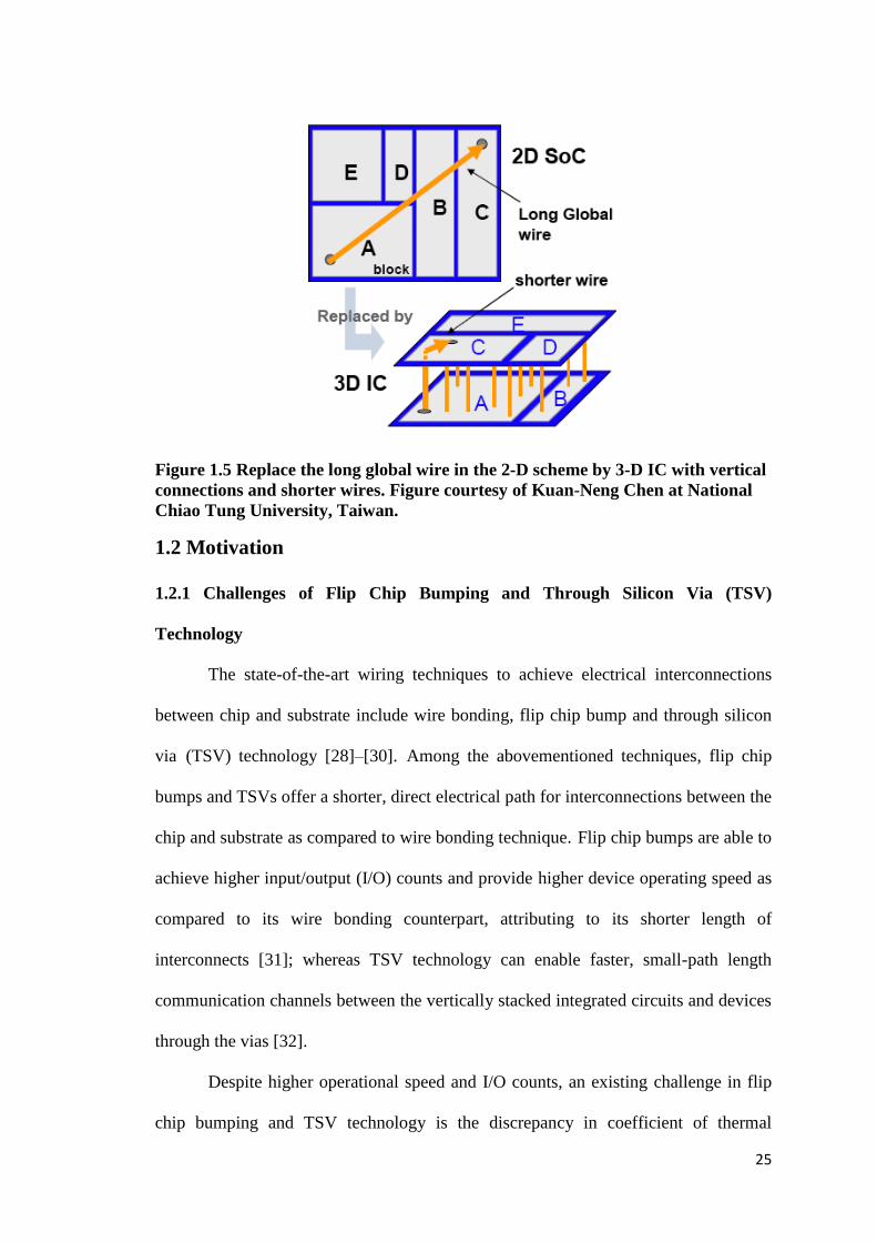
both 2-D SiP and SoC, 3-D integration scheme can be employed. As shown in Figure
1.4(c), the 3-D integration scheme involves electrical connections between the logic
and the memory components via vertical interconnects. Due to the structural nature of
3-D integration scheme, much shorter interconnects are needed (as illustrated in Figure
1.5), where the memory latency can be significantly reduced, resulting in improved
chip performance.

24
Figure 1.4 Schematic diagrams showing the difference between 2-D and 3-D
interconnects (Source: Beyne [27] ): (a) 2-D SiP integration; (b) SoC integration;
(c) 3-D integration. Reprinted with permission from [27], © 2006 IEEE.
25
Figure 1.5 Replace the long global wire in the 2-D scheme by 3-D IC with vertical
connections and shorter wires. Figure courtesy of Kuan-Neng Chen at National
Chiao Tung University, Taiwan.
1.2 Motivation
1.2.1 Challenges of Flip Chip Bumping and Through Silicon Via (TSV)
Technology
The state-of-the-art wiring techniques to achieve electrical interconnections
between chip and substrate include wire bonding, flip chip bump and through silicon
via (TSV) technology [28]–[30]. Among the abovementioned techniques, flip chip
bumps and TSVs offer a shorter, direct electrical path for interconnections between the
chip and substrate as compared to wire bonding technique. Flip chip bumps are able to
achieve higher input/output (I/O) counts and provide higher device operating speed as
compared to its wire bonding counterpart, attributing to its shorter length of
interconnects [31]; whereas TSV technology can enable faster, small-path length
communication channels between the vertically stacked integrated circuits and devices
through the vias [32].
Despite higher operational speed and I/O counts, an existing challenge in flip
chip bumping and TSV technology is the discrepancy in coefficient of thermal

26
expansion (CTE) between copper bump/TSV-filler and its surrounding materials.
Copper is widely used in the flip chip bumps and via fillings due to excellent electrical
and mechanical properties, favourable compatibility with the back-end of line (BEOL)
processes. However, due to the large CTE mismatch between silicon (2.3×10⁻⁶/˚C)
and copper (17 × 10-6/˚C) [33], Cu-based pillar bumps and TSVs fabricated on Si
substrate arises numerous electrical stability and reliability issues, especially under
high temperature fluctuations. The CTE mismatch issue is particularly prominent for
TSVs. Due to the large CTE mismatch between silicon and copper, the fabrication
process can induce substantial thermomechanical stresses in silicon around the vias,
resulting in thermomechanical failure in the device [34], [35]. In a typical TSV
deposition process, an annealing step at a higher temperature (e.g. 200 C) is applied
after the Cu electroplating in order to stabilize the Cu grain structures and relax the
stresses in Cu. Upon cooling down to the room temperature, copper contracts much
faster and pulls the surrounding silicon, inducing thermomechanical stresses in the
silicon area around the vias. The TSV-induced stresses can cause reliability problems
such as copper via extrusion and interfacial delamination [36]–[40], and undesirable
mobility shifts in devices through the piezoresistivity effect [41], [42]. As most
devices are located within a sub-micron depth from the wafer surfaces, the design
rules with the near-surface TSV-stress awareness and stress-resulting carrier mobility
change are crucial for the successful implementation of 3-D ICs.
Extrusions of Cu vias are frequently observed in the TSV structures upon
undergoing high temperature excursion. The via pop-up phenomenon can cause
interfacial failure of a TSV (Figure 1.6(a)) and/or cracking in Si near the lower ends of
TSVs (Figure 1.6(b)) during the thermal processing [43]. The via-extrusion can be
accompanied by interfacial delamination, as shown in Figure 1.6(c).

27
Figure 1.6 Reliability problems in TSV structures [43]: (a) Interfacial
delamination; (b) Silicon cracking; (c) Via extrusion (Pop-up). Figure is from
online web source: Cho, S. [43].
As mentioned earlier, piezoresistivity effect in interconnects may cause
undesirable mobility shifts in the device. Consequently, TSV-induced stresses will
result in variations in electron-hole mobility’s in devices, leading to non-uniformity,
uncontrollable device performances. To resolve this issue, most IC designers will be
informed about the Keep-out-zone (KOZ) when designing devices with TSV
structures. KOZ is defined as the area surrounding each TSV where all logic cells
must “keep out” to avoid being influenced by the TSV-induced stresses. In actual
designing of TSVs-included devices, the presence of abundant TSVs largely occupies
the available floor space on 3D-IC layout. Additional KOZ areas further reduces the
available floor space, where smaller area of KOZ is desirable to save circuit design
floor space as illustrated in Figure 1.7.
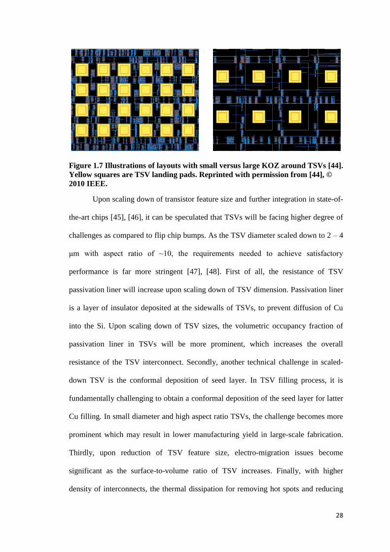
28
Figure 1.7 Illustrations of layouts with small versus large KOZ around TSVs [44].
Yellow squares are TSV landing pads. Reprinted with permission from [44], ©
2010 IEEE.
Upon scaling down of transistor feature size and further integration in state-of-
the-art chips [45], [46], it can be speculated that TSVs will be facing higher degree of
challenges as compared to flip chip bumps. As the TSV diameter scaled down to 2 – 4
μm with aspect ratio of ~10, the requirements needed to achieve satisfactory
performance is far more stringent [47], [48]. First of all, the resistance of TSV
passivation liner will increase upon scaling down of TSV dimension. Passivation liner
is a layer of insulator deposited at the sidewalls of TSVs, to prevent diffusion of Cu
into the Si. Upon scaling down of TSV sizes, the volumetric occupancy fraction of
passivation liner in TSVs will be more prominent, which increases the overall
resistance of the TSV interconnect. Secondly, another technical challenge in scaled-
down TSV is the conformal deposition of seed layer. In TSV filling process, it is
fundamentally challenging to obtain a conformal deposition of the seed layer for latter
Cu filling. In small diameter and high aspect ratio TSVs, the challenge becomes more
prominent which may result in lower manufacturing yield in large-scale fabrication.
Thirdly, upon reduction of TSV feature size, electro-migration issues become
significant as the surface-to-volume ratio of TSV increases. Finally, with higher
density of interconnects, the thermal dissipation for removing hot spots and reducing

29
thermal migration becomes more critical in 3-D ICs.
1.2.2 Advantages of Carbon Nanomaterials
In recent years, carbon nanomaterials, graphene and carbon nanotubes (CNTs)
have emerged as promising materials for the integration in the next-generation
advanced packaging technologies [28], [49], [50]. The main benefits of carbon
nanomaterials, e.g. CNTs, lie in their excellent electrical, thermal and mechanical
properties: (i) low electrical resistivity, measured in a range of 0.8~33.8 mΩ •cm for
single CNT and CNT bundles [51]–[54]; (ii) high current density ~109 A/cm2 in single
CNT [55]; (iii) high thermal conductivity, reported in a range of 600-3,000 W/mK for
individual multi-walled carbon nanotubes (MWCNTs) [56], [57]; and (iv) closer CTE
to Si (2.3 × 10⁻⁶/˚C) as compared to Cu (17 × 10-6/˚C), e.g. single-walled carbon
nanotubes (SWCNTs) ~2 × 10⁻⁶/˚C [58].
Table 1.1 shows the comparison of typical physical properties between Si, Cu
and carbon nanotube (CNT) at room temperature. Besides the smaller CTE with Si,
the loosely-packed nature of CNT bundles can also ease the thermomechanical stress
introduced in the Si substrate [59]. These advantages enable carbon nanomaterials to
be a highly attractive candidate as both on-chip and off-chip interconnects in 3-D ICs.
Currently, substantial works have been reported for the fabrication and
characterization of CNT TSVs on conductive metal lines [60]–[62]. Meanwhile, CNT
bumps have been demonstrated as the potential flip chip bumps by several
groups[63]–[65]. Apart from CNTs, graphene has also been proposed as a potential
candidate to augment copper as the next-generation planar interconnects due to its
patterning feasibility and current carrying capacity [66]–[69].
30
Table 1.1 Typical physical properties of Si, Cu and CNT at room temperature
[70].
Material Young
Modulus
(GPa)
Poisson’s
Ratio
Thermal
Conductivity
(W/mK)
Electrical
Resistivity
(Ω⋅m)
CTE
(𝟏𝟎−𝟔/ ˚C)
Silicon
(Si)
169 along
<110>
130 along
<100>
(anisotropic)
0.064 along
<110>
0.28 along
<100>
(anisotropic)
149 1×10⁻¹
to
4×10−6*
2.3
Copper
(Cu)
128 0.34 385 1.68×10⁻⁸ 16.4
Carbon
Nanotube
(CNT)
1300 0.0344 3500 0.29×10⁻⁸
to
1.2 ×10⁻⁸
[73]
Axial:
-0.6**
Trans.:
6.6**
* The resistivity of silicon depends strongly on the presence of impurities in the
material
**CNT CTE is an average value as there is a range found in the literature
1.2.3 Full Carbon-Based Interconnects
Recently, a concept of full carbon-based interconnects is proposed by
implementing graphene-CNT heterostructures in BEOL and TSVs for 3-D ICs and
packages as a higher-performance alternative to their copper counterparts [71]. Hybrid
carbon nanostructures, e.g. the pillared CNT-graphene nanostructure shown in Figure
1.8 [72], are speculated as one of the graphene-CNT hetero-structures which can be
potentially applied in the 3-D integration. Benefiting from the combination of one-
dimensional (1-D) nanotubes and two-dimensional (2-D) graphene, 3-D graphene-
CNT hetero-structure possesses desirable out-of-plane properties [73]–[75] while
maintaining the in-plane properties. Attributing to the speculated benefits of this
structure, it has attracted numerous innovative applications including new efficient
electrodes for fuel cells [76], nano-porous structures for hydrogen storage [72] and
supercapacitors [77], tailored orthogonal thermal transport materials [75] and building
blocks for nano/microscale integrated devices [78], [79].

31
Figure 1.8 Pillared CNT-graphene nanostructure with 3D network [72].
Reprinted with permission from [72], © 2008 American Chemical Society.
Currently, various successful attempts for the fabrication of graphene-CNT
hybrid structures [80]–[83]have been done reported. One of the pioneering studies of
the graphene-CNT hybrid structures is reported by Y.S. Kim et al [73], where hybrid
graphene-CNT structure comprising of out-of-plane CNTs grown on the graphene
layer is fabricated and its electrical properties are characterized. Y. Zhu et al [84]
developed a method to bond graphene and single-wall carbon nanotubes (SWCNTs)
seamlessly (Figure 1.9(a)), which shows an ohmic contact formed between the bonded
CNTs and graphene (Figure 1.9(b)). This study reports the first observation of the
covalent transformation of sp2 carbon between the planar graphene and the vertical-
aligned SWCNTs under the atomic resolution by scanning transmission electron
microscopy (STEM) (Figure 1.10). On the other hand, a novel carbon composite
structure of multi-layered graphene combined with the upper ends of vertically aligned
multi-wall CNTs (MWCNTs) on the substrate has been synthesized (Figure 1.11(a))
[23]. One of the unique features of this graphene-CNT composite is the self-
organization within the atomic structure of the multi-layered graphene, prior the CNT
growth. Attributing to the self-organizing nature, the upper ends of CNTs can be
electrically connected to each other via the graphene (Figure 1.11(b)) [85]. On the

32
other hand, a similar hybrid material with graphene film tightly connected with the
upper ends of the CNT arrays has also been reported, synthesized by a two-step
chemical vapor deposition (CVD) process [80]. In general, most graphene-CNT hybrid
structures are fabricated via CVD method during the CNT growth stage.
Most recently, a demonstration shows that the full integration of intercalation-
doped multi-layer graphene (MLG) wires and CNT vias offer higher performance and
better reliability as compared to the Cu interconnects at 5nm node [80]. Another
successful fabrication of graphene-CNT heterostructure for the off-chip interconnects
was made through a direct growth of CNTs within the vias and on top of the graphene
[33]. To form a complete full-carbon 3-D interconnection, the assembly process of the
top graphene layer after CNT growth shall be further explored.

33
Figure 1.9 (a) Scheme and SEM results for the synthesis of SWCNTs directly
from graphene and (b) I–V measurements [84]. Reprinted with permission from
[84], © 2012 Macmillan Publishers Limited.

34
Figure 1.10 TEM and STEM images of CNT–graphene junctions [84]. Reprinted
with permission from [84],© 2012 Macmillan Publishers Limited.

35
Figure 1.11 SEM images of (a) synthesized graphene/CNT composite and (b)
TEM images around the connection between graphene and CNTs [85]. Reprinted
with permission from [85], © 2008 The Japan Society of Applied Physics.
1.3 Objective
In this thesis, the possibilities of implementation of the graphene-CNT hetero-
structure in through silicon vias (TSVs) for novel 3-D interconnects will be explored.
In this approach, vertical-aligned CNTs and graphene will be integrated into 3-D
interconnect structures. Vertical-aligned will be developed to replace the conventional
metal in TSVs, while graphene will be developed to replace the traditional horizontal
metal lines. The key challenges include, but not limited to (1) process development in
growing high density CNT bundles above bottom graphene electrode within TSVs, (2)
accurate transfer of a top graphene layer onto the as-grown CNT bundles, (3) atomic
fusion between transferred graphene and CNTs to form carbon covalent bonds to
reduce CNT-graphene contact resistance, (4) microstructural and electrical
characterization of CNT-graphene structure to justify the occurrence of atomic fusion
between CNT bundles and graphene layer. Several objectives are intended to be
achieved as follows:

36
1) Feasibility study of the CNT growth on the graphene under experimental
conditions
2) Process design and development to grow high-density CNT bundles within TSVs
3) Process development of transferring graphene layer onto the as-grown CNT
bundles
4) Microstructural studies of the fabricated structures (by Raman, SEM and TEM)
5) Electrical studies of the fabricated structures (by I-V measurements)
6) Development and exploration of the femtosecond laser annealing condition for the
fusion of transferred graphene and CNTs
1.4 Major Contributions of Thesis
One of the significant outcomes of this thesis is the successful demonstration
of CNT growth on the bottom graphene electrodes within TSVs. First of all, the
fabrication processes of top wafer with TSVs of various diameters (5-50μm) and
bottom wafer with patterned graphene electrodes and catalyst deposition were
successfully developed. Next, top TSV wafer and bottom graphene wafer were bonded
and manually grounded, followed by subsequent wet and dry etching steps to
completely remove the handling wafer and buried oxide exposing the underlying
TSVs. Finally, CNT growth was carried out using thermal CVD (TCVD) approach
within the TSVs on the bottom graphene electrodes. As compared to the free-standing
CNT growth with sufficient length (~334 μm) and high density (estimated as ~1011
cm-2), inhibited growth of CNTs are obtained within the TSVs. The inhibited growth
of CNTs can possibly be attributed to several process-engineering steps involved, e.g.
wafer-bonding, grinding and wet/dry etching. Further modification and optimization
of the process steps need to be done in order to attain higher density of CNT fillings
within the unfilled TSVs.

37
Upon growing of CNT bundles on graphene electrode within TSVs, transfer
process of a top graphene layer onto the as-grown CNT bundles was successfully
performed with direct graphene-to-CNT contact at the interface. Four-point-probe
(4PP) I-V characterization suggests that an ohmic contact was achieved between the
graphene and CNTs. Low CNT bump resistance of 2.1Ω for 90,000 µm2 CNT area
including the CNT/graphene contact resistance was obtained, demonstrating reduction
of contact resistance with additional graphene layer on the CNT bundles. The thesis
presents preliminary outcomes for the assembly process of transferring a top-graphene
layer onto CNTs, and the electrical properties of direct graphene-to-CNT contact. The
obtained outcomes provide an insightful understanding on the application of CNT-
graphene structures in electrical interconnects, paving the way for the implementation
of full carbon-based 3D interconnects.
1.5 Organization of Thesis
This thesis is organized into 8 main chapters. Chapter 1 outlines the
introduction of the research work carried out in this doctorate study. Chapter 2
introduces the literature review and the state-of-the-art of the relevant studies which
have been reported. Chapter 3 reports the development and optimization of CNT
growth on graphene layer. Chapter 4 demonstrates CNT growth within TSVs on top of
the graphene electrodes. Chapter 5 explores the transfer of graphene onto the top of
CNT bundles to physically secure the top graphene layer onto the CNT tips. Chapter 6
characterizes the electrical properties of direct graphene-to-CNT contact. Chapter 7
explores the feasibility of using femtosecond laser annealing for graphene-CNT fusion.
Finally, Chapter 8 outlines the conclusion of this research, and the possible future
continuation works from this research.

38
Chapter 2 : A Review of Carbon Nanotubes (CNTs) for Through
Silicon Via (TSV) Interconnects
2.1 Through Silicon Vias (TSVs)
A critical structural element in the 3-D integration is the through silicon via
(TSV) [27], [86], [87], as shown in Figure 2.1. TSV provides a preferable alternative
to the long wiring in the 2-D schemes by vertical connections between the stacked dies.
The use of TSVs in 3-D integration can effectively improve system performance and
reduce manufacturing costs. However, the TSV fabrication process is technically-
challenging due to the involvement of Deep Reactive Ion Etching (DRIE) to create
through-structure deep hole for the accommodation of the Cu-based interconnect.
Figure 2.1: 3-D integration using TSV structures: (a) Illustration of TSVs. Figure
courtesy of Chuan Seng Tan at Nanyang Technological University, Singapore. (b)
TSV samples. Figure is from online web source: Ron Maltiel [88] .

39
The fabrication of TSVs involves three key processes [89]–[92] : 1) via hole
etching, 2) TSV materials filling, and 3) Si wafer thinning and wafer
bonding/debonding. For a reliable and efficient TSV fabrication, each of the three
processes needs to be optimized. In general, DRIE, also known as the “Bosch” process,
is applied to fabricate the through-substrate-deep hole vertically within the silicon
wafer for via etching process.
However, careful control of the Bosch process is needed to prevent formation
of scallop-shaped sidewalls (Figure 2.2(a)) [36], [92] . Formation of scallop-shaped
sidewalls can be attributed to under-optimization of DRIE process, where the
scalloped contours hinder the conformal deposition of barrier and seed layer. Non-
conformal barrier and seed layer may increase the susceptibility of Cu (widely used
via-filling material) diffusion into Si, resulting in under-filling of TSVs [93]. Under-
filling of TSVs may result in the occurrence of voids and pinholes within the TSV Cu
pillars (Figure 2.2(b)) [94], directly affecting the device reliability. In addition, the
thinning-down process of the Si substrate by chemical-mechanical polishing (CMP)
could cause wafer warpage (Figure 2.2(c)) [95], which leads to subsequent problems
in 3-D stacking. To address various processing issues, several processing flows have
been investigated [92], [96], [97]. As of today, two TSV integration processes are
mostly used in the semiconductor industry: ‘via-middle’ and ‘via-last’ processes. The
main difference in these two processes is the sequence of the TSV formation relative
to the wafer thinning and wafer bonding/debonding processes.

40
Figure 2.2 Processing issues: (a) scallops at sidewall, where TEOS is an insulating
liner material [92]; (b) voids inside TSV [94]; (c) wafer warpage [98]. Reprinted
with permission from [92] [94] [98] , © 2008, 2010 IEEE.
Via-middle process
Figure 2.3 illustrates the via-middle process, which is performed following the
FEOL fabrication process. A typical via-middle process flow to fabricate TSVs with a
diameter of 10 μm and a depth of 50 μm in the Si substrate is described as follows.
First, lithography is carried out to pattern the TSV openings across the wafer. Next,
DRIE is used to fabricate the TSV holes of desired dimensions. Then, an oxide liner of
~1 μm thickness is deposited within the TSV holes. The oxide layer (dielectric layer)
reduces capacitance and improves electrical isolation between the TSVs and the Si
substrate. In some cases, instead of oxide, polymeric dielectric materials [99], [100]
such as benzocyclobutene (BCB) or parylene have been deposited as the sidewall
insulators. To prevent diffusion of Cu into the Si substrate, a thin barrier layer (~50nm)
of Ta/TaN or Ti/TiN is deposited. For Cu electroplating, a thin Cu seed layer is first

41
deposited in the TSVs, followed by Cu electroplating process to filled the pre-
fabricated TSVs. A subsequent annealing step could be applied to stabilize the Cu
grain structures and relax the thermomechanical stresses in Cu for further processing.
At the final stage of the TSV fabrication, CMP is carried out to remove the Cu
overburden, top Ta/TaN and oxide layers, and to planarize the wafer surface. The
fabrication of TSV structures is followed by the BEOL process in which interconnects
are made and bonding pads are patterned. Finally, the Si substrate is thinned down to
the optimized TSV height (~50 μm).
Figure 2.3 Via-middle process for TSV structures. Figure is from online web
source: Yannou, J. [101]
Via-last process
The via-last process involves similar processes as described in the previous
sections, including etching of TSV holes and deposition of dielectric layer and barrier
layers. However, although the final structure constructed by the via-middle or via-last
process could be the identical, the process sequence used in the via-last process
(Figure 2.4) is quite different from the via-middle process. In the via-last process, both
FEOL and BEOL structures are first fabricated on the Si wafer. Then, the wafer is
thinned down up to the depth that is optimized for the TSV height. This is then
followed by etching of the via holes from the back side of wafer to reach the interface
of BEOL interconnect lines, and filling the holes by the sequence of dielectric layer,
Ta/TaN barrier layer, Cu seed, electroplating of Cu, and finally a CMP process.

42
Figure 2.4 Via-last process for TSV structures. Figure is from online web source:
Yannou, J. [101] .
2.2 Growth and Fabrication of CNT TSVs
CNT growth and via-filling in TSVs can be done by two distinct process flows,
either by growing CNT bundles directly in TSVs in a bottom-up approach, or
otherwise by transferring CNT bundles, pre-growth, into the TSVs. For the bottom-up
approach, catalyst layer shall first be deposited onto the bottom of TSVs first,
followed by CNT growth using CVD method. Three catalyst deposition methods are
commonly used for CNT growth: sputtering, e-beam evaporation and chemical
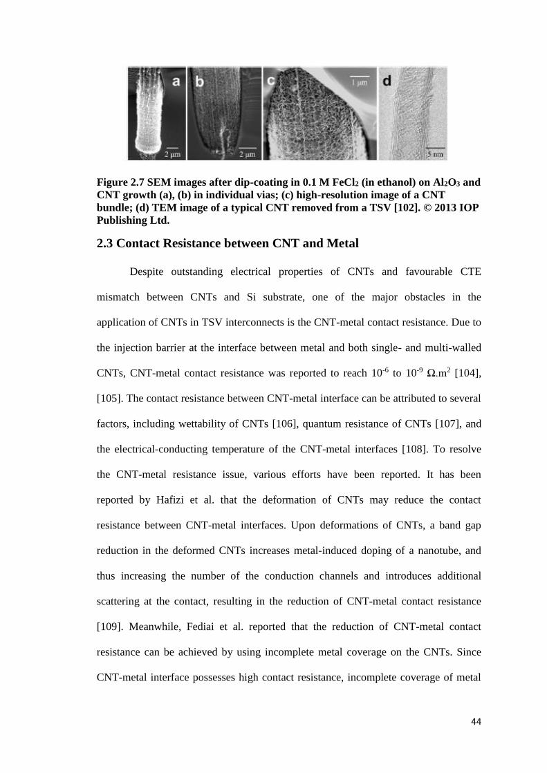
deposition. Previous works done by R Xie et al [102] shown that sparsely-grown
CNTs are obtained from sputtered catalyst layer at the bottom of TSVs (aspect ratio 5-
10), possibly due to insufficient catalyst deposition at the bottom of TSVs (Figure 2.5).
It can be explained that the mean free path of catalyst in a sputtering chamber is
relatively short as compared to the distance between targeted material and the
substrate during the sputtering process. On the other hand, e-beam evaporation-
deposited catalyst can grow vertically-aligned CNT bundles from the bottom of vias
openings. However, TSVs were only partially filled by CNTs grown using e-beam
evaporation-deposited catalyst (Figure 2.6). Due to the isotropic nature of the
evaporation process, not all vias are directed in parallel to the direction of evaporation.
As a result, vias that are not parallel to the evaporation direction receive limited
catalyst deposition. Apart from sputtering and e-beam evaporation, catalyst deposited
by chemical method (e.g. dip-coating in a FeCl2 solution) is found to be an alternative

43
method for realizing the bottom-up vertical-aligned CNTs fully filled the TSV holes
(Figure 2.7).
The main disadvantage of the bottom-up approach for CNT growth is that it
requires high growth temperatures, approximately 700˚C to fully-fill the TSVs [53]
which is incompatible with conventional CMOS process (usually <400˚C). For the
sake of compatibility with CMOS technology, successful TSV filling by a low-
temperature CNT transfer process at 200 ˚C has been reported, replacing the direct
growth of CNTs in the vias [29]. However, the post-growth transfer process is limited
to large diameter TSVs [103], as small diameter (<30μm) TSV structures exhibit
stringent alignment accuracy, hindering it from large scale, repetitive manufacturing
process [29], [103].
Figure 2.5 SEM images of CNT forest on top of the TSV pattern: Fe-catalyst
placement is done by sputtering on Al2O3 layer using (a) 1 nm, (b) 2 nm and (c) 3
nm Fe [102]. © 2013 IOP Publishing Ltd.
Figure 2.6 SEM images of CNT bundles grown inside the TSV vias with Al2O3
and an evaporated thin film of (a) 2 nm, (b) 3 nm, (c) and 4 nm Fe, with in (d) a
zoom-in of the 2 nm Fe result [102]. © 2013 IOP Publishing Ltd.
44
Figure 2.7 SEM images after dip-coating in 0.1 M FeCl2 (in ethanol) on Al2O3 and
CNT growth (a), (b) in individual vias; (c) high-resolution image of a CNT
bundle; (d) TEM image of a typical CNT removed from a TSV [102]. © 2013 IOP
Publishing Ltd.
2.3 Contact Resistance between CNT and Metal
Despite outstanding electrical properties of CNTs and favourable CTE
mismatch between CNTs and Si substrate, one of the major obstacles in the
application of CNTs in TSV interconnects is the CNT-metal contact resistance. Due to
the injection barrier at the interface between metal and both single- and multi-walled
CNTs, CNT-metal contact resistance was reported to reach 10-6 to 10-9 Ω.m2 [104],
[105]. The contact resistance between CNT-metal interface can be attributed to several
factors, including wettability of CNTs [106], quantum resistance of CNTs [107], and
the electrical-conducting temperature of the CNT-metal interfaces [108]. To resolve
the CNT-metal resistance issue, various efforts have been reported. It has been
reported by Hafizi et al. that the deformation of CNTs may reduce the contact
resistance between CNT-metal interfaces. Upon deformations of CNTs, a band gap
reduction in the deformed CNTs increases metal-induced doping of a nanotube, and
thus increasing the number of the conduction channels and introduces additional
scattering at the contact, resulting in the reduction of CNT-metal contact resistance
[109]. Meanwhile, Fediai et al. reported that the reduction of CNT-metal contact
resistance can be achieved by using incomplete metal coverage on the CNTs. Since
CNT-metal interface possesses high contact resistance, incomplete coverage of metal

45
on CNT bundles can reduce the contact resistance, enhancing the overall electrical
properties of the CNT-based interconnects [110].
Besides the abovementioned strategies, an effective approach in reducing the
CNT-metal contact resistance is to introduce graphitic layers between the CNT-metal
interfaces. Due to the formation of C-C bond between the graphitic layer and the
CNTs, the CNT-metal contact resistance can be significantly reduced [111]. One of
the commonly reported graphitic layers to be incorporated onto CNT interconnects is
graphene. Due to the abundant presence of graphitic sp2 bond and its associated
unique electrical properties, graphene has been reported to reduce the CNT-metal
contact resistance [112]. However, despite potential benefits from the hetero-structure,
limited studies have been reported on the fabrication and application of Graphene-
CNT structures in TSV interconnects.
2.4 Fabrication of Graphene-CNT Heterostructure
One of the pioneering works reported on the fabrication of planar graphitic-
CNT hetero-structure is graphite-CNT structure. Labunov et al. has reported
successful fabrication of multi-level composite nanostructures based on the arrays of
vertically aligned CNTs and planar graphite layers. In the reported work, graphite-
CNT structure is fabricated using a one-step injection CVD technique, utilizing high
temperature catalytic pyrolysis of fluid hydrocarbon. It opens a way to the three-
dimensional functional devices creation, in particular, multi-level graphite (graphene)
very large scale integrated circuits with the vertical commutations on the basis of
CNTs [113]. Meanwhile, Ghosh et al. reported CNT filling of TSVs, with graphene
layers as electrical linings at the bottom of the TSVs. Upon including of graphene
layers onto CNT-based TSV fillings, the contact resistance between CNTs and the
underneath metal surface has been significantly reduced. At the same time, the CNT-

46
graphene heterostructure has approximately 15 times higher thermal conductivity of
the carbonaceous materials compared to copper. providing excellent pathways for the
effective heat-transfer from hotspots to the heat-sinks in multi-chip stacked
configurations [114]. On the other hand, Jiang et al. introduces full integration of
multilayer graphene and CNT vias, enabled by a unique carbon-nickel alloycontact
technology. Owing to the extremely high current carrying capacity, thermal
conductivity and large carrier scattering length of carbon nanomaterials, the reliability
of the all-carbon interconnect technology is demonstrated to surpass that of Cu [115].
Despite availability of various works on CNT/graphene integration, the
application of CNT-graphene onto TSV interconnect application is still under-
explored. Therefore, exploratory and development work on the growth, fabrication,
and characterizations of CNT-graphene heterostructure for TSV interconnect
applications is called for.
2.5 Annealing Methods for Metal-CNT Fusion
In accordance to the proposed graphene-CNT heterostructure, a stable and low-
resistance ohmic contact at graphene/CNT interface plays a major role for its
application in 3-D interconnects. However, limited work has been reported on the
fusing of graphene sheets onto CNT tip. In this thesis, possible annealing methods are
explored by investigating the effect of various thermal treatments onto the CNT/metal
interface. Fundamentally, CNT-graphene fusion can be achieved by thermal annealing
to enhance the crystallinity within the CNT-graphene interface [116], [117]. Thermal
annealing is a commonly-used method to improve the contact resistance between
CNTs and metal electrodes [111], [118]. Y. Zhang et al [119] reported achievement of
a low-resistance contact between single-wall carbon nanotubes (SWCNTs) and
transition metal electrodes via a controlled solid–solid reaction (Figure 2.8) under

47
elevated temperature (800-1000˚C). Apart from that, they found that the low-
resistance contact originates from the formation of a crystalline heterostructure of
CNT/metal carbide at the interface (Figure 2.8, suggesting the formation of chemical
bonds between CNTs and metal carbide (TiC) after the thermal annealing [119].
Meanwhile, J. Lee et al [120] reported prolonged stable contacts with low resistance
between the CNTs and the Ti–Au electrodes using rapid thermal annealing (RTA)
under low temperatures (600-800˚C). However, for integration of CNTs in silicon-
based applications, thermal annealing exhibits serious technical challenges as silicon-
based devices have lower thermal tolerance in general, where thermal-induced failure
will possibly occur in high temperature (>600˚C) conditions.
Using an electric current-induced Joule-heating annealing method, on the other
hand, was demonstrated as an alternative way to modify the contact resistance between
CNTs and metal. Annealing can be carried out through resistive heating of the
substrate where CNTs are grown. By pulsed electrical annealing, Y. Woo et al [121]
reduced the contact resistance between an individual single-wall carbon nanotube
(SWCNT) and palladium (Pd) electrodes without destroying the field effect transistor
devices.
Apart from the joule heating by chamber-heating or resistive heating, recent
works have suggested pulsed laser annealing (PLA) as a favorable heating technique,
especially in the fabrication of semiconductor thin films [122]. Utilizing a high
intensity, short laser pulse to irradiate the sample, PLA creates either a melting front
that subsequently solidifies into a single or polycrystalline material, or thermal heating
in solid phase within the short laser pulse. Due to the non-destructive, rapid heating, of
PLA, it has been considered as one of the most promising methods for the thermal-
fusion of graphene and CNTs.

48
Figure 2.8 (a) Schematic illustration of the method for fabricating
nanotube/carbide heterostructure by solid-solid reaction (M=Metal) [119]. ©
1999 AAAS. (b) TEM and High-resolution TEM images of the interface between
TiC and SWCNT bundle [119]. © 1999 AAAS.

49
Chapter 3 : Free-Standing CNT Growth on the Graphene
3.1 Introduction
As discussed in the previous chapters, graphene-CNT heterostructure possesses
numerous benefits and exhibits promising potential towards its application in future 3-
D interconnects. Vertically-aligned MWCNT bundles grown on the graphene are the
preferred choice in through silicon vias (TSVs) for novel 3-D interconnects. Two
commonly explored techniques to achieve vertical alignment within CNTs are by
thermal chemical vapor deposition (TCVD) and plasma enhanced chemical vapor
deposition (PECVD). Generally, TCVD-grown MWCNTs have smaller diameter with
higher area density as compared to PECVD-grown MWCNTs.
Numerous researches have been reported to investigate the growth mechanism
of CNTs on metal lines. However, growing CNTs directly on metal lines is
challenging, as metallic catalyst will diffuse into metal surface during CNT growth,
due to the requirement of elevated temperature (600~800˚C) during CNT growth [123].
A solution to the diffusion of metallic catalyst is to introduce a barrier layer that
blocks unwanted catalyst diffusion into the metal lines. However, can CNTs grown
directly on graphene layer, or a barrier layer is still necessary, despite the presence of
graphene? Thus, it is necessary to study the growth of CNTs on the graphene.
3.2 Experimental Objective and Scope
Despite the presence of prior studies reporting about CNT growth on graphene,
significant discrepancies on the methodology, techniques, and outcomes can still be
found across various reported studies. To realize the application of CNT-graphene
heterostructure in TSV interconnects, it is important to investigate the feasibility of
CNT growth on graphene layer. To optimize CNT growth on graphene layer with
TCVD technique, effects of temperature profile and Fe catalyst thickness on the

50
morphological structure of grown CNTs were carefully studied. This is to obtain
optimized CNT growth condition for its latter application in filling TSV voids with
graphene bottom electrodes, which will be discussed in the next chapter.
3.3 CNT Growth Method
Aixtron Black Magic System was used for the growth of vertical-aligned
MWCNTs under thermal CVD (TCVD) mode. The key advantage of this system is the
presence of a shower head with patented design, located vertically above the substrate.
This unique design allows the gases to be distributed uniformly across the 2" diameter
substrate, leading to the growth of high uniformity CNTs. The picture of the
deposition system and the description of available growth mode in Aixtron Black
Magic System are shown in Figure 3.1.
Figure 3.1 Photograph of Aixtron Black Magic CVD system (left). The various
growth modes and CNTs types available using Aixtron Black Magic system
(right).
In TCVD mode, iron (Fe) catalyst aluminum oxide (Al2O3) or Al/Al2O3 barrier
layers are optimized in the manufacturer-default CNT growth recipes available in
Aixtron Black Magic system. The optimum thickness of typical Fe catalyst reported in
the literature is 1-2 nm [124]. As it is technically challenging to measure Fe catalyst

51
film of 1-2 nm using conventional thin film measurement equipment, the deposition
time of Fe film will be used as an indication to gauge the Fe thickness, using the
known deposition speed of 0.1~0.2 Å/sec.
It has been reported that CNTs grown from Fe catalyst on Al2O3 barrier layer
possess high crystallinity structure with vertically-aligned CNT morphologies [50],
[125]. However, one major drawback is that Al2O3 has low electrical conductivity,
hindering its applicability in CNT-based interconnects. It has been reported that Al2O3
barrier layer of ≥ 4nm thickness exhibits high resistivity, which will affect the overall
electrical conductivity of the CNT/metal interface due to formation of non-ohmic
contact. Meanwhile, omitting the Al2O3 barrier layer may solve the non-ohmic contact
issue, but employing pure Al barrier layer result in the formation of sparsely-grown,
short CNTs, which is undesirable for TSV interconnect applications [28]. Thus, a
combination of Al and Al2O3 is preferred for TSV interconnect CNTs as it takes both
factors into consideration: functionality and electrical properties of the barrier layer.
By varying permutations of Al/Al2O3 layers thickness, the most preferable
combination of barrier layers was optimized to be 8 nm Al/2 nm Al2O3 with a low
resistivity of 2.7 x 10⁻⁶ Ω∙cm [50], [125].
In a typical TCVD growth process, acetylene (C2H2) is used as the carbon
feedstock gas, where hydrogen (H2) is used as the etchant. A typical cycle of TCVD
growth ranges between 1 to 5 min depending on the required length of CNTs. The
typical growth cycle of CNTs using TCVD technique is shown in Figure 3.2. As
shown in Figure 3.2, “Ramping up” refers to the increase in heater temperature
accompanied by flow of H2 gas, “Pre-growth” refers to pre-growth of CNTs with
slightly lower temperature than the actual growth stage, whereas “CNT growth” refers
to the actual growth process, where the growth temperature is ramped up from the

52
“Pre-growth” stage, reaching the actual CNT growth temperature
Figure 3.2 Temperature profile of a typical TCVD growth cycle. The growth time
can vary from 1 to 5 min.
3.4 Effects of Temperature Profile and Fe Catalyst Thickness
To obtain vertically-aligned CNTs with high crystallinity, the TCVD growth
recipes for CNTs are optimized, varying various parameters such as durations and
temperatures in annealing, pre-growth, growth, and post-growth stages. Pre-growth
and growth stages refer to preliminary growth of CNTs with lower temperature and
actual growth of CNTs with higher temperature, as described in the previous section.
Annealing stage refers to the pre-growth annealing of Fe catalyst under continuous H2
flow, whereas post-growth stage refers to annealing of CNTs after the growth process
under continuous H2 flow. At the same time, to optimize the growth recipe, Fe
thickness, and C2H2/H2 gas flows are varied. Considering all variable factors, 3 growth
recipes were explored, as shown in Table 3.1. Recipe #1 contains an annealing process
at 500˚C and a pre-growth at 600˚C. Recipe #2 contains an annealing process at 500˚C
and a post-growth at 700˚C but without the pre-growth process. Recipe #3 only had a

53
direct CNT growth at 700˚C without the annealing process or pre-/post-growth. The
CNT growth temperature for the three recipes was fixed at 700˚C. To understand the
effect of the 3 investigated growth recipes on the quality of the obtained CNTs,
preliminary characterizations are carried out, including CNT height and its associated
Raman spectra, as summarized in Figure 3.3 and Table 3.1. From the obtained results,
direct CNT growth at 700˚C without the pre-/post-growth yields the highest length and
IG/ID peak ratio among the investigated recipes, indicating high degree of CNT
crystallinity. Using the same growth recipe, the CNTs grown from 1.1nm and 2.2nm
Fe catalyst show the similar IG/ID peak ratio, suggesting that the catalyst thickness has
limited impact on the CNTs’ crystallinity.
To understand further, growth temperature is varied individually to investigate
its impact on the obtained CNTs. By using similar CNT growth duration (2 min)
without the annealing process or pre-/post-growth, the growth temperature is varied
from 550˚C to 700˚C. The obtained CNT heights and morphological characteristics are
shown in Table 3.2 and Figure 3.4, respectively. It can be observed that the CNTs
grown at 550˚C were not aligned well vertically and had a porous structure with
relatively sparse inter-tube spacing as compared to CNTs grown at 600˚C and 700˚C.
Also, the length of CNTs grown at 550˚C is shorter than those grown at 600˚C and
700˚C. Thus, in order to have a vertically-aligned CNT growth with the adequate
length and high density, the minimum CNT growth temperature should be around
600~700˚C.

54
Table 3.1 Recipe tuning for MWCNT growth
Recipe No. #1 #2 #3
Annealing Temp.(°C) 500 500 500 500 - -
Annealing Time(s) 15 15 15 15 - -
Pre-growth Temp.(°C) 600 600 - - - -
Pre-growth Time(s) 30 30 - - - -
Growth Temp.(°C) 700 700 700 700 700 700
Growth Time(s) 270 270 300 300 300 300
Post-growth Temp.(°C) - - 700 700 - -
Post-growth Time(s) - - 120 120 - -
Barrier layer Al 8nm/Al2O3 2nm
Fe thickness(nm) 1.1 2.2 1.1 2.2 1.1 2.2
H2 Flow (sccm) 600 600 600 600 600 600
C2H
2 Flow (sccm) 200 200 200 200 200 200
CNT growth length(µm) 88 140 180 157 235 244
1000 1200 1400 1600 1800 2000
G
D
Inte
nsit
y (
a.u
.)
Raman shift (cm-1)
recipe 1
recipe 2
recipe 3
1.1nm Fe
1000 1200 1400 1600 1800 2000
G
D
2.2nm Fe
In
ten
sit
y (
a.u
.)
Raman shift (cm-1)
recipe 1
recipe 2
recipe 3
Figure 3.3 Raman spectra images of CNT growth using three different recipes
with 1.1/2.2nm Fe as catalyst.
Table 3.2 Density and length of CNT growth with the same growth time (2 min)
under different temperature (550, 600 and 700 ˚C).
Avg. CNT growth length (µm)
Temp. (˚C) 1.1nm Fe 2.2nm Fe
550 3.0 3.5
600 28 19
700 101 105

55
Figure 3.4 SEM images of CNTs grown on 2nm Fe with the same growth time (2
min) under (a) 550 ˚C, (b) 600 ˚C and (c) 700 ˚C.
3.5 Growth of Patterned CNT Pillars on the Graphene
Graphene-deposited wafers used in this section were purchased commercially
(4" silicon wafers with 470nm SiO2 with a 7cm × 7cm double-layer transferred
graphene) from Hangzhou Gelanfeng Nanotechnology Co., Ltd. The full wafer was
manually cleaved into small dies with 12mm × 12mm dimension before processing.

56
The crystallinity of the purchased graphene wafers was carefully checked by optical
and Raman microscopy (Raman system: Witec Alpha 300R) before processing.
Catalyst/barrier layer was deposited on the graphene with lift-off process. Negative
photoresist (ma-N 1440) was used to pattern the area for catalyst/barrier layer
deposition. 8nm Al, 2nm Al2O3 and 1.1nm Fe were sequentially deposited by e-beam
evaporation. Pre-growth and CNT growth temperatures were set as 600/700˚C
respectively, with 30s and 300s as the pre-growth and CNT growth durations,
respectively. Temperature ramping speed was set as 100 ˚C /min. C2H2 and H2 gas
flow during CNT growth were set as 200/600 sccm respectively. Figure 3.5 shows the
SEM images of patterned CNT pillars grown on the graphene layer, showing dense,
vertically-aligned CNTs with ~334 μm height which is sufficient for TSV interconnect
application. The average diameter of CNTs was ~5 nm as shown in TEM images
(Figure 3.6). CNT (ρ) can be estimated using the following equation:
ρ =𝐹×𝑆
𝜋(𝑑2⁄ )2
where F is the filling factor ratio defined as the surface area covered with CNTs after
densification over the surface area before densification, S is the surface area before
densification, d is the average diameter of CNTs. To determine the filling ratio, bumps
of 1 mm2 were patterned (not shown) on each sample and subjected to same growth
process. The densification process was performed by immersing the sample in IPA.
The filling factor was calculated to be 0.132 ± 0.008 by using imaging software pixel
calculation based on more than 10 CNT bumps. Subsequently, the surface density of
CNTs can be calculated to be ~1011 cm-2.
The grown CNTs can be postulated to have high level of defectively due to low
IG/ID peak ratio (Figure 3.7(a)). This reflects on the IG/ID peak ratio of CNTs grown on
graphene, where the CNT-graphene hetero-structure exhibits wider D peak with higher

57
intensity as compared pristine graphene (Figure 3.7(b)), indicating the formation of
amorphous carbon on the graphene sheet. The formation of amorphous carbon can
possibly due to the pre-growth step which was carried out at relatively low
temperature (600˚C).
Figure 3.5 SEM images of patterned CNT pillars grown on the graphene layer.
Figure 3.6 Transmission electron microscopy (TEM) images of the as-grown
CNTs.

58
1000 1200 1400 1600 1800 2000
a)
D
G
Inte
nsit
y (
a.u
.)
Raman shift (cm-1)
1000 1500 2000 2500 3000 3500
b)G
D
Inte
nsit
y (
a.u
.)
Raman shift (cm-1)
before CNT growth
after CNT growth
Figure 3.7 Raman spectra images of (a) as-grown CNTs and (b) graphene
before/after CNT growth.
3.6 Summary
In this chapter, recipes and methodology to grow free-standing CNTs on
graphene sheet has been explored and optimized. TCVD approach yields sufficient
length (~334μm) and high density (estimated as ~1011 cm-2) CNT growth. Different
growth parameters such as catalyst film thickness, growth time and growth
temperature have been systemically studied. With the understanding of different
growth parameters, the feasibility in growing CNTs within TSVs on the bottom
graphene electrodes will be explored.

59
Chapter 4 : CNT Growth within TSVs on the Bottom Graphene
Electrodes
4.1 Introduction
The state-of-the-art, industrial standard TSV technology prefers copper as the
TSV-filler material due to its compatibility with the back-end of line (BEOL)
processes, along with suitable electrical and mechanical properties of copper material.
However, a technical challenge lies within Cu TSVs is the coefficient of thermal
expansion (CTE) difference between copper and its surrounding materials, which is
mainly silicon. Due to the relatively large mismatch of CTE between silicon (2.3×10⁻⁶
/˚C) and copper (17 × 10-6 /˚C), Cu TSVs give rises to many stability and reliability
problems during chip operation, especially under high temperature fluctuation
conditions.
The newly emerged concept of full carbon-based interconnects are expected to
have numerous advantages over their copper counterparts. The advantages include: 1)
less thermal mismatch stress in TSVs than Cu due to the low CTE and porous nature
of CNTs; 2) favorable heat dissipation properties due to the high thermal conductivity
of CNTs and graphene; and 3) possibly lower contact resistance of the CNT/graphene
interface as compared to the CNT/metal interface.
4.2 Experimental Objective and Scope
In this chapter, bottom-up growth of CNTs on the bottom graphene electrode
within TSVs is demonstrated. A fabrication process flow was designed and optimized
to investigate the possibility of replacing the horizontal metal lines and metal-filled
TSVs with graphene-CNT heterostructure. The introduction of extra fabrication steps
onto the free-stranding CNT growth mentioned in Chapter 3 will expose the catalyst to
foreign environments and adversely affect the growth of CNTs. Finally, the fabricated

60
structure was characterized by optical microscopy, Raman and SEM.
4.3 Designed Fabrication Process Flow
The designed fabrication process flow contains three parts: 1) top wafer with
TSV etching, 2) bottom wafer with graphene patterning and catalyst deposition 3)
process steps after top and bottom wafers bonding, as shown in Figure 4.1. For top
wafer processing, silicon-on-insulator (SOI) wafer is used as the starting wafer for the
fabrication. First, channel etching was designed to form a space for the
accommodation of graphene and catalyst layers on the bottom wafer. After that, TSV
holes and electrical probing trench were etched. On the other hand, bottom graphene
electrodes were patterned on a graphene wafer, followed by the catalyst patterning and
deposition on the graphene electrodes. The top and bottom wafers were then bonded,
followed by the removal of top handling wafer and buried oxide layer of the SOI to
expose the underlying TSV holes. Finally, CNT growth was carried out within the
TSVs using TCVD technique.
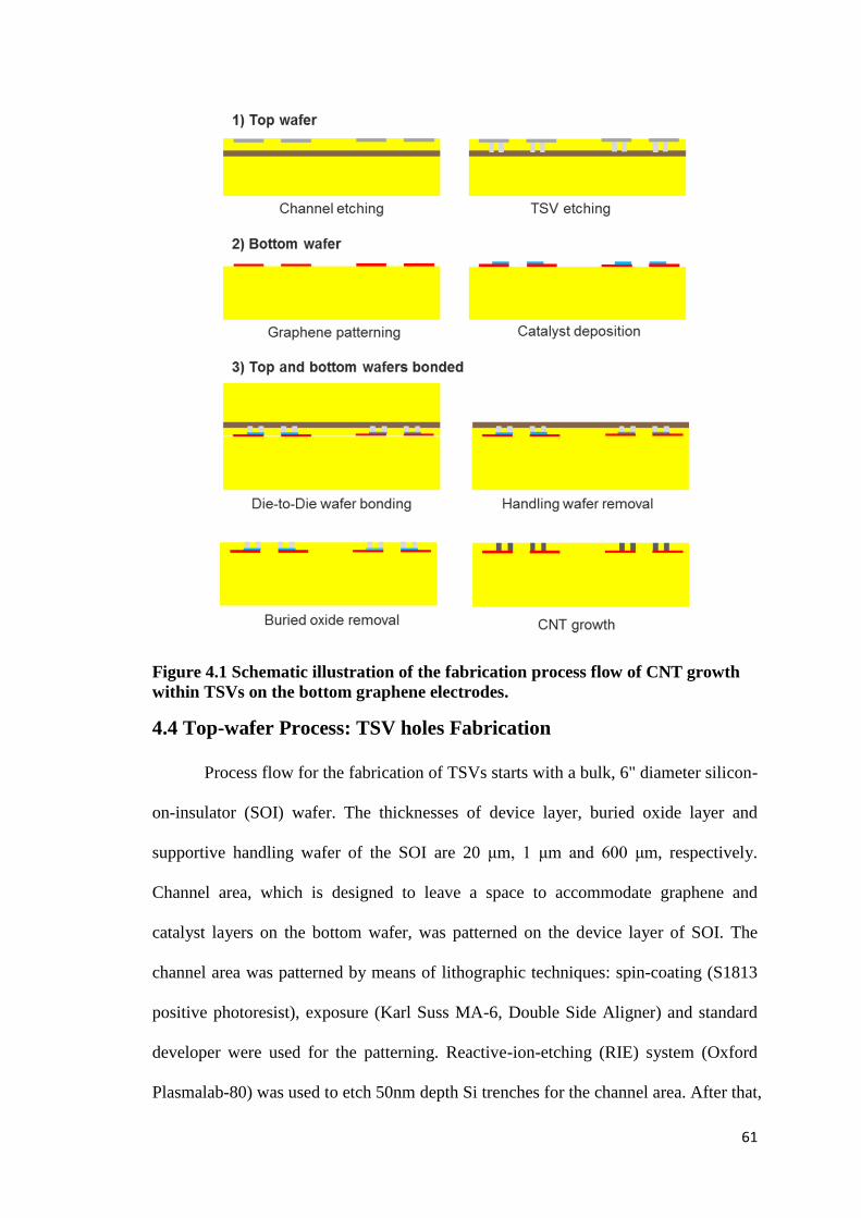
61
Figure 4.1 Schematic illustration of the fabrication process flow of CNT growth
within TSVs on the bottom graphene electrodes.
4.4 Top-wafer Process: TSV holes Fabrication
Process flow for the fabrication of TSVs starts with a bulk, 6" diameter silicon-
on-insulator (SOI) wafer. The thicknesses of device layer, buried oxide layer and
supportive handling wafer of the SOI are 20 μm, 1 μm and 600 μm, respectively.
Channel area, which is designed to leave a space to accommodate graphene and
catalyst layers on the bottom wafer, was patterned on the device layer of SOI. The
channel area was patterned by means of lithographic techniques: spin-coating (S1813
positive photoresist), exposure (Karl Suss MA-6, Double Side Aligner) and standard
developer were used for the patterning. Reactive-ion-etching (RIE) system (Oxford
Plasmalab-80) was used to etch 50nm depth Si trenches for the channel area. After that,

62
the probing trench and circular holes of desired parameters were patterned using the
abovementioned lithographic method. The designed diameters of TSVs vary from 5-
50μm. Deep-Reactive-Ion-etching (DRIE) system (SAMCO's RIE-800iPB) was used
to form 20 µm deep TSV holes through the device layer till the buried oxide stop, via
the widely-used BOSCH process. After removing the photoresist hard-mask, the full
wafer was sent into the furnace for thermal oxidation in order to form an oxide layer
(~100nm) on the sidewall of TSVs for electrical insulation. The full wafer was then
diced into small dies with 10mm x 10mm dimension. Figure 4.2 shows the SEM
results of the fabricated TSVs with 5, 15 and 50μm diameters. As shown in the SEM
images, the vias exhibit straight sidewalls without much over-etching at the bottom of
the TSVs. Here, vias of different diameters were fabricated through to the buried oxide
etch-stop, with a highest aspect ratio of ~4 for 5μm diameter.
Figure 4.2 SEM images of the cross-section of TSVs with (a) 5, (b) 15 and (c)
50μm diameters (depths are all 20μm).
4.5 Bottom-wafer Process: Graphene Patterning and Catalyst
Deposition
Graphene wafers used in this chapter are purchased commercially, where 4"
diameter silicon wafers (with SiO2 470nm) are deposited with a 7cm x 7cm single-
layer transferred graphene (Hangzhou Gelanfeng Nanotechnology Co., Ltd). The full
wafer was manually cleaved into small dies with 12mm x 12mm dimension before
processing. The crystallinity of the original graphene wafers was carefully checked by

63
optical and Raman microscopy (Raman system: Witec Alpha 300R) prior to
lithography processing. Standard lithography processes: spin-coating (AZ5214
positive photoresist), exposure (MJB4 Karl SUSS Mask Aligner) and developing were
used for patterning of graphene as the bottom electrodes. O2 plasma etching (1 min, 60
W, 20 sccm oxygen flow) was carried out in the RIE system (Oxford Plasmalab-80) to
etch off exposed graphene area. The recipe of O2 plasma etching was optimized to
completely remove the graphene layer without over-etching to the SiO2 underneath.
After graphene patterning, catalyst/barrier layer was deposited on the graphene
electrodes using lift-off process. Negative photoresist (ma-N 1440) was used to pattern
the area for catalyst/barrier layer deposition. 8 nm Al, 2 nm Al2O3, and 1.1 nm of Fe
were sequentially deposited using e-beam evaporator at nominal vacuum of 5 x10⁻⁶
mbar at low temperature (<80˚C) conditions. Deposition speed was set around 0.1~0.2
Å/sec. The top thin Al/Al2O3 layer acts as an anti-diffusion barrier for the catalyst Fe
during the high temperature process of the CNT growth, as mentioned in the previous
chapters.
Figure 4.3 shows the optical images of the substrate after graphene patterning
and catalyst deposition. No visible cracks/peeling-off of the graphene was observed
after the lithography process. The crystallinity of graphene was also verified by Raman
microscopy before and after lithography process, which shows no significant increase
of ID (~1350cm-1)/IG (~1580cm-1) peak ratio, i.e. no severe graphene degradation
(Figure 4.4).

64
Figure 4.3 Optical images (with 5x, 20x and 50x magnification) after graphene
patterning and catalyst deposition: long strips are patterned graphene electrodes
and round circles are deposited catalyst/barrier layers.
1000 1500 2000 2500 3000 3500
2D
G
D
G
2D
Inte
nsit
y (
a.u
.)
Raman shift (cm-1)
Before lithography
After lithography
D
Figure 4.4 Raman spectra images of the graphene before and after lithography
process.
It is well-known that residue photoresists can adhere to the electrode surface
after lithography process, resulting in severe interface contamination. In this work, the
interface contamination due to the residue photoresists on the graphene electrodes can
cause significant increasing in the contact resistance between the graphene and CNTs.
Two methods commonly used in conventional semiconductor cleaning process:
plasma cleaning or UV-ozone (UVO) treatment, may also be used to clean the
graphene surface before catalyst deposition. On the other hand, the following wafer
bonding process requires an activation step with the plasma or UVO treatment on the
wafer surface for fusion bonding. Thus, the quality of graphene electrodes before/after
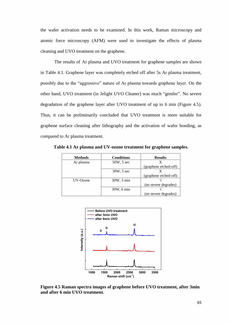
65
the wafer activation needs to be examined. In this work, Raman microscopy and
atomic force microscopy (AFM) were used to investigate the effects of plasma
cleaning and UVO treatment on the graphene.
The results of Ar plasma and UVO treatment for graphene samples are shown
in Table 4.1. Graphene layer was completely etched off after 5s Ar plasma treatment,
possibly due to the “aggressive” nature of Ar plasma towards graphene layer. On the
other hand, UVO treatment (in Jelight UVO Cleaner) was much “gentler”. No severe
degradation of the graphene layer after UVO treatment of up to 6 min (Figure 4.5).
Thus, it can be preliminarily concluded that UVO treatment is more suitable for
graphene surface cleaning after lithography and the activation of wafer bonding, as
compared to Ar plasma treatment.
Table 4.1 Ar plasma and UV-ozone treatment for graphene samples.
Methods Conditions Results
Ar plasma 50W, 5 sec X
(graphene etched-off)
30W, 5 sec X
(graphene etched-off)
UV-Ozone 30W, 3 min √
(no severe degrades)
30W, 6 min √
(no severe degrades)
1000 1500 2000 2500 3000 3500
G'G
D
Inte
nsit
y (
a.u
.)
Raman shift (cm-1)
Before UVO treatment
after 3min UVO
after 6min UVO
Figure 4.5 Raman spectra images of graphene before UVO treatment, after 3min
and after 6 min UVO treatment.

66
Figure 4.6 shows the topography images of (a) pristine graphene layer, (b)
graphene layer after lithography process and (c) patterned graphene layer after 3min
UVO treatment. The graphene’s root mean square (RMS) of the surface roughness
increased from 1.28 nm (Figure 4.6(a)) to 4.41 nm (Figure 4.6(b)) and subsequently
decreases to 3.45 nm (Figure 4.6(c)). The pristine graphene shows a RMS of 1.28 nm
possibly due to PMMA residue after the graphene transfer process. Poly methyl-
methacrylate (PMMA) layer is commonly used as a polymer support layer during the
mechanical transfer process of the graphene onto the Si wafer, and will be removed at
the end of the transfer process. Similar to photoresist residue, PMMA cannot be
thoroughly removed with solvents and a thin residue layer will usually be found on the
graphene surface. After lithography process, the increasing of roughness can be
attributed to the resists residue present on the graphene surface. The surface appears
smoother after 3 min UVO cleanness and the RMS decreased ~1 nm, indicating
effective removal of resist residuals by UVO cleaning.
Figure 4.6 AFM topography images (top-row 3D and bottom-row 2D) of 10μm x
10μm area of a) pristine graphene, b) graphene after lithography and c) graphene
after lithography following a 3min UVO treatment.

67
4.6 Die-to-Die Wafer Bonding and Exposure of TSV holes
The two wafers, top TSV die and bottom graphene die, are then bonded face-
to-face in a die-to-die bonder machine (FINEPLACER® matrix) by top-side
alignment marks at normal temperature and atmospheric condition using the fusion
bonding approach. 6 min UVO treatment was used as the activation step for bonding
process without damaging the bottom graphene electrodes. Two dies were successfully
bonded with good bonding strength. In order to expose the underlying TSV holes for
CNT growth, the handling wafer and buried oxide layer of the top SOI wafer needs to
be removed. However, the thickness of the handling wafer is too thick (~600μm) to be
removed by conventional micro-fabrication techniques. To remove wafer of such
thickness, grinding process is usually used, but the process is not suitable for small die
(10mm x10mm) samples. Since limited grips are anticipated on the die during the
grinding process, the risk of die dislodging, damaged/missing during the process is
significant. On the other hand, KOH wet etching is an alternative method for wafer
removal. But the practical etching rate of Si in KOH solution is ~60μm/hour in 80˚C
20% KOH solution, which means that it will take ~10 hours to etch-off all the 600μm
silicon and not practical for large-scale, seamless fabrication.
Nevertheless, a trial process was done to remove the handling wafer by
manually grinding (300~400μm depth) following a KOH wet etching (200~300 μm
depth). After that, the exposed buried oxide was removed by RIE. Figure 4.7 shows
the pictures of a die after the grinding and KOH etching process which, where the
remaining buried oxide layer is not uniform. From the optical images, it can be seen
that holes at the perimeter area (Figure 4.7(a)) were over-etched by KOH, where the
over-etching is not found at TSVs in the middle portion of the die (Figure 4.7(b)).
After buried oxide removal, it can be seen that there are some color changes in via

68
holes at different regions of the die (Figure 4.8). For example, TSVs at the ‘top left’
and ‘bottom left’ regions are green (i.e. the color of original 550nm SiO2) and purple
(i.e. ~450nm SiO2) at the ‘top right’ region. This phenomenon occurs as manual
grinding process will generally produce low surface uniformity throughout the whole
die. The remaining Si thickness at the ‘top right’ region was thinner than the ‘top left’
or ‘bottom left’ regions. Due to the uneven Si thickness after grinding, the remaining
Si at the ‘top right’ region was completely etched-off, leading to the over-etching of
underlying buried oxide. Meanwhile, the Si layer at the ‘top left’ and ‘bottom left’
regions is still under-etched. Thus, the exposed buried oxide has thinner thickness at
the ‘top right’ region as compared to ‘top left’ and ‘bottom left’ regions. Eventually,
when RIE was applied to remove the buried oxide for via holes open, the ‘top right’
region was over-etched down to the bottom oxide layer of bonded wafer, resulting in
the color changes of TSVs.
Figure 4.7 Optical images after the handling wafer removal: TSV holes (a) at the
perimeter area and (b) in the middle portion of the die; (c) photo of a real sample
after the grinding and KOH etching process.

69
Figure 4.8 Optical images after the handling wafer and buried oxide removal:
exposed TSVs at (a) top left, (b) top right, (c) bottom left and (d) bottom right
region of the die.
4.7 CNT Growth within TSVs
After opening of TSV holes, the whole die was transferred into the Axitron
Black Magic System for vertical-aligned multi-wall carbon nanotubes (MWCNTs)
growth under the thermal CVD (TCVD) mode with hydrogen (H2) and acetylene
(C2H2) gas flows. Pre-growth and CNT growth were set at 600/700˚C with
30sec/30min, respectively. C2H2 and H2 gas flows during the CNT growth were set as
200/600 sccm respectively. On the other hand, a sample of bottom die which has
undergone graphene patterning and catalyst deposition process (similar conditions as
mentioned in Chapter 3) was used for comparison.
As shown in Figure 4.9, we can see that CNT growth was inhibited and
severely affected within the unfilled TSV (20μm diameter) despite that the growth
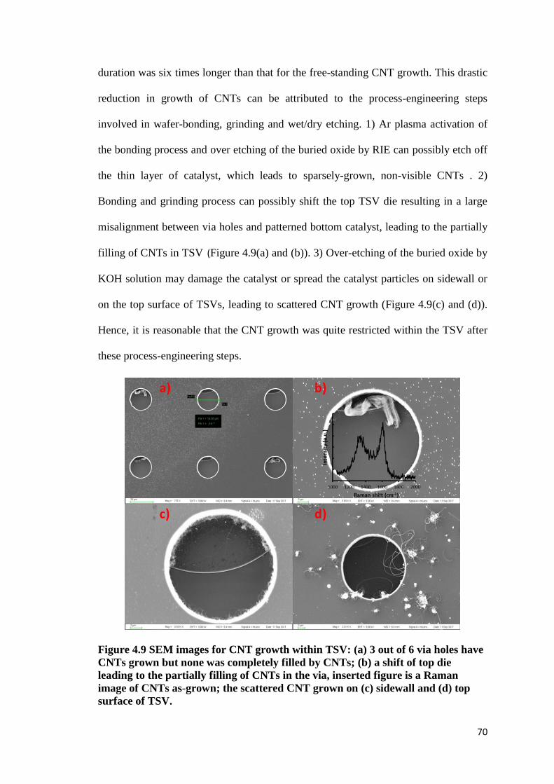
70
duration was six times longer than that for the free-standing CNT growth. This drastic
reduction in growth of CNTs can be attributed to the process-engineering steps
involved in wafer-bonding, grinding and wet/dry etching. 1) Ar plasma activation of
the bonding process and over etching of the buried oxide by RIE can possibly etch off
the thin layer of catalyst, which leads to sparsely-grown, non-visible CNTs . 2)
Bonding and grinding process can possibly shift the top TSV die resulting in a large
misalignment between via holes and patterned bottom catalyst, leading to the partially
filling of CNTs in TSV (Figure 4.9(a) and (b)). 3) Over-etching of the buried oxide by
KOH solution may damage the catalyst or spread the catalyst particles on sidewall or
on the top surface of TSVs, leading to scattered CNT growth (Figure 4.9(c) and (d)).
Hence, it is reasonable that the CNT growth was quite restricted within the TSV after
these process-engineering steps.
Figure 4.9 SEM images for CNT growth within TSV: (a) 3 out of 6 via holes have
CNTs grown but none was completely filled by CNTs; (b) a shift of top die
leading to the partially filling of CNTs in the via, inserted figure is a Raman
image of CNTs as-grown; the scattered CNT grown on (c) sidewall and (d) top
surface of TSV.

71
4.8 Summary
In this chapter, fabrication process flow of graphene-CNT heterostructure
within TSVs was designed and explored. As compared to the free-standing growth of
CNTs on the graphene, CNTs grown within the unfilled TSV holes are relatively
sparse owing to the process-engineering steps involved in wafer-bonding, grinding and
wet/dry etching. Process steps of TSV fabrication for CNT growth shall be modified
and optimized in order to improve the CNT fillings within the unfilled TSVs. On the
other hand, in order to form a complete full-carbon 3-D interconnection, the assembly
process of the top graphene layer after CNT growth needs to be explored, which will
be further discussed in the following chapters.

72
Chapter 5 : Process Exploration of Transferring a Top-Graphene
Layer onto CNTs
5.1 Introduction
In Chapter 4, direct growth of CNTs within TSVs on the bottom graphene
electrodes has been demonstrated. In order to form a complete full-carbon 3-D
interconnection, the assembly process of the top graphene layer after CNT growth
needs to be explored. The assembly process includes: (1) transferring a top-graphene
layer onto the as-grown CNTs and (2) fusion of transferred graphene and CNTs to
enhance the conductivity and reliability of the graphene/CNT contact. Process (1) will
be explored in this chapter and Chapter 6, while process (2) will be explored in
Chapter 7.
5.2 Experimental Objective and Scope
This chapter aims to explore the process of transferring a top-graphene layer
onto the CNTs for the formation of CNT-graphene heterostructure, and to study the
electrical properties of the fabricated structure. Three test structures (i.e. single-side
step structure, double-step structure and bridge structure) were designed and fabricated
for CNT growth and top-graphene layer transfer. Meanwhile, three transferring
methods of graphene layer (i.e. direct dry transfer, dry transfer with a thermal tape and
wet transfer) were explored using the single-side step structure after CNT growth.
From the electrical results, the best test structure and transferring method will be
selected and optimized for the electrical characterizations of direct graphene-to-CNT
contact in the next chapter.

73
5.3 Design and Fabrication of the Test Structures for Electrical Study
To investigate the electrical properties of the top-graphene layer transferred on
the CNTs, a single-side step structure was initially designed for preliminary researches.
Figure 5.1 illustrates the proposed structure and fabrication process flow. First, a ~100
μm depth step was etched in the silicon substrate using DRIE dry etching or KOH wet
etching techniques as shown in Figure 5.1(a)-(c). After that, the remaining SiO2 was
etched off using buffered oxide etching (BOE) (Figure 5.1(d)) followed by ~280 nm
thermal oxide growth (Figure 5.1(e)) to form an insulation layer from the conductive
Si substrateAfter that, 20nm Ti/100nm Au electrodes were deposited on both lower
and higher side of the step followed the deposition of barrier/catalyst layer (8nm
Al/2nm Al2O3/1.1nm Fe) only on the lower side of the step, as shown in Figure 5.1(f).
CNT growth was carried out and the growth recipe was tuned to obtain CNTs of
similar heights with the step (Figure 5.1(g)). A layer of graphene will then be
transferred on top of CNTs and the Au electrode on the unetched silicon surface
(Figure 5.1(h)). Two or Four-point-probe (2PP/4PP) I-V measurements will be used
for the electrical characterizations of this fabricated step structure.
Figure 5.1 (a)-(g) Fabrication process flow of the single-side step structure and (h)
a top-graphene layer transferred on CNTs after CNT growth.

74
Figure 5.2 shows the SEM images of the samples after CNT growth in the
steps etched by (a) KOH wet etching and (b) DRIE dry etching, respectively. The
height of CNT growth was fine-tuned to be similar to the depth the step. However,
from Figure 5.2, it can be observed that KOH-etched step exhibits a 54.7˚ sloped
sidewall due to the anisotropic nature of KOH etching. As a result, a large gap existed
between the top of vertical-aligned CNTs and the edge of the step. CNTs grown in
KOH-etch step also exhibit uneven heights, as shown in Figure 5.2(a). On the other
hand, the vertical sidewalls are observed on the DRIE-etched step, with smaller gaps
between the CNTs and the edge of the step, with CNTs heights of high uniformity.
Thus, DRIE is chosen as the preferred method for the fabrication of the step structure.
Figure 5.2 SEM images of the samples after CNT growth with the steps etched by
(a) KOH wet etching and (b) DRIE.
With the single-side step structure, the graphene layer was successfully
transferred on the top of CNTs and preliminary I-V results of the fabricated structure
were obtained. However, there were some questionable issues which require further
investigation and verifications. The details of these will be discussed in the following
section. At the same time, to further characterize the electrical properties of the
graphene layer transferred on CNTs, double-side step structure and bridge structure
were designed.

75
Figure 5.3 illustrates the fabrication process flow of double-side step structure
with a top-graphene layer transferred on grown CNTs. The advantages of double-side
step structure include: (1) avoid the possibility of sidewall shortage; (2) symmetry
structure with more flattened graphene contact to the CNTs; (3) I-V measurement
result of Au-graphene-Au can be obtained from the structure to calculate the CNT
bump resistance (𝑅𝐴𝑢−𝐶𝑁𝑇−𝐺 ). The possible underlying issues of double-side step
structure and the associated feasibility in resolving them will be discussed in the
following section.
Figure 5.3 (a)-(g) Fabrication process flow of the double-side step structure and
(h) a top-graphene layer transferred on CNTs after CNT growth.
The bridge structure illustrated in Figure 5.4 is an optimization of the double-
side step structure. The two steps in the bridge structure are only used for the supports
for free-standing CNTs and the top Au electrodes on the steps are eliminated. A gap is
present between two bottom Au electrodes to facilitate the probing and electrical
characterizations of the Au-CNT-graphene-CNT-Au structure after graphene transfer.
Large, uncertain contact resistances between the transferred graphene and Au
electrodes in the double-side step structure can be avoided in the bridge structure
(details will be discussed in the following section).

76
Figure 5.4 Top-view and side-view illustrations of the bridge structure (a) before
and (b) after graphene transfer with the thermal tape.
5.4 Transferring Methods of Graphene Layer
Graphene samples used in this chapter were intrinsic CVD graphene grown on
the Cu foil with a Polymethyl methacrylate (PMMA) layer coated on the top of
graphene. The “float graphene” samples are made by etching off the Cu foil and
transferring the PMMA/graphene layer on the top of sandpaper with a dimension of
10mm × 10mm for delivery (supplied by Hangzhou Gelanfeng Nanotechnology Co.,
Ltd). Thus, the “float graphene” can be directly peeled off, i.e. the PMMA/graphene
layer (as shown in Figure 5.5(a)), from the sandpaper for the following transfer
process. Different colors can be observed in Figure 5.5(a) due the non-uniform PMMA
layer and the grain boundaries of poly crystal graphene, which was also observed in
Figure 5.5(a). Raman characterization indicates that the obtained graphene is a single
layer graphene as shown in Figure 5.5(b).

77
Figure 5.5 (a) Optical and (b) Raman images of the “float graphene”
(PMMA/graphene layer).
Three transferring methods of graphene layer were proposed and conducted in
this section. The single-side step structure after CNT growth was used for the trials of
transfer processes. Figure 5.6 shows the optical and SEM images after different
graphene transfer processes. The first method is direct dry transfer. The
PMMA/graphene layer was peeled off from the sandpaper and then directly placed on
the top of CNTs. After the transfer process, the graphene layer was mechanically
pressed down onto the CNTs to make a better contact between the graphene and CNTs.
From Figure 5.6(a), it can be observed that PMMA/graphene layer was creased after
the transfer process. The PMMA/graphene layer is not flatten with visible wrinkles,
making it highly susceptible to breaking and damaging as the PMMA/graphene layer
is extremely thin and fragile. An improved method is to perform the dry transfer
process with a thermal tape. The thermal tape increased the stiffness of the
PMMA/graphene layer to obtain more flattened layer wrinkles, which may be
potential break point of the layer (Figure 5.6(b)). The third method is wet transfer in
the DI water. First, the PMMA/graphene layer was peeled off from the sandpaper and
allowed to float on the DI water. After that, the single-side step structure with the CNT
growth was dipped into the water, tilted 45º to fish the PMMA/graphene layer out.
78
Figure 5.6(c) shows the result after the wet transfer process. It can be observed that
most CNTs collapsed after dipping into DI water except CNTs located around the step
region, where the CNT heights are shorter compared to other growth regions. Despite
obtaining flattened graphene was flattened at the edge of the step, no physical contact
was established with the CNTs around the edge of the step because CNT lengths
around the region were too short and insufficient to form physical contact. From the
comparisons of the three transferring methods, dry transfer technique with the thermal
tape is chosen as the primary technique for graphene transfer.

79
Figure 5.6 Optical and SEM images after three different graphene transfer
processes: (a) direct dry transfer, (b) dry transfer with a thermal tape and (c) wet
transfer in the DI water.
5.5 Results and Discussion
Figure 5.7(a) and (b) show the SEM images of the single-side step structure
before and after graphene direct dry transfer. The electrical characterization results of
2PP I-V measurements (Keithley 4200-SCS Semiconductor Characterization System)
between Au electrodes on the lower side and the higher side of the step before and
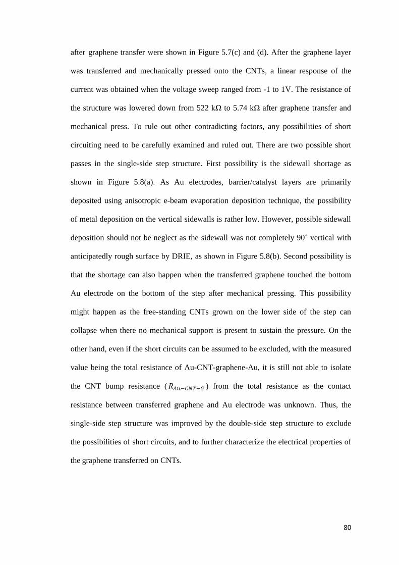
80
after graphene transfer were shown in Figure 5.7(c) and (d). After the graphene layer
was transferred and mechanically pressed onto the CNTs, a linear response of the
current was obtained when the voltage sweep ranged from -1 to 1V. The resistance of
the structure was lowered down from 522 kΩ to 5.74 kΩ after graphene transfer and
mechanical press. To rule out other contradicting factors, any possibilities of short
circuiting need to be carefully examined and ruled out. There are two possible short
passes in the single-side step structure. First possibility is the sidewall shortage as
shown in Figure 5.8(a). As Au electrodes, barrier/catalyst layers are primarily
deposited using anisotropic e-beam evaporation deposition technique, the possibility
of metal deposition on the vertical sidewalls is rather low. However, possible sidewall
deposition should not be neglect as the sidewall was not completely 90˚ vertical with
anticipatedly rough surface by DRIE, as shown in Figure 5.8(b). Second possibility is
that the shortage can also happen when the transferred graphene touched the bottom
Au electrode on the bottom of the step after mechanical pressing. This possibility
might happen as the free-standing CNTs grown on the lower side of the step can
collapse when there no mechanical support is present to sustain the pressure. On the
other hand, even if the short circuits can be assumed to be excluded, with the measured
value being the total resistance of Au-CNT-graphene-Au, it is still not able to isolate
the CNT bump resistance ( 𝑅𝐴𝑢−𝐶𝑁𝑇−𝐺 ) from the total resistance as the contact
resistance between transferred graphene and Au electrode was unknown. Thus, the
single-side step structure was improved by the double-side step structure to exclude
the possibilities of short circuits, and to further characterize the electrical properties of
the graphene transferred on CNTs.

81
Figure 5.7 SEM images of the single-side step structure (a) before and (b) after
graphene direct dry transfer; (c) illustrations and (d) results of 2PP I-V
measurements between Au electrodes on the lower side and the higher side of the
step before and after graphene transfer.

82
Figure 5.8 (a) Sidewall shortage in the single-side step structure and (b) SEM
images of the sidewall > 90˚ with rough surface
Figure 5.9 (a) and (b) show the tilted-view and side-view SEM images of the
double-side step structure after CNT growth. It can be observed that the CNT length in
the middle area (~avg. 10 μm) was too short to reach the height of the step (~70 μm).
This can be attributed to the inhibited the gas flow in the trench between two steps
which affects the grown length of CNTs. After CNT growth, a graphene layer was
transferred using the dry transfer with a thermal tape, and mechanically pressed to
make a better contact between the transferred graphene and CNTs, as shown in Figure
5.10. Large gaps can be observed between the bottom Au electrode with CNTs grown
on the top and the sidewalls of two steps, indicating that the possible shortages
between the bottom Au electrode/CNTs and the top Au electrodes on two steps can be

83
omitted. Figure 5.11(a) and (b) show the illustrations and results of 4PP I-V
measurements before and after the graphene transfer. Top electrode A to B, top
electrode A to bottom electrode C and bottom electrode C to top electrode B were
probed correspondingly. I-V measurement of two top electrodes A to B (i.e. Au-
graphene-Au) shows the linear response to the current when the voltage sweep was
applied, indicating that ohmic contact was achieved between the graphene and Au
electrodes. However, the collapse of free-standing CNTs can still happen when
mechanical pressure is applied after the graphene transfer. Since the CNT length was
much shorter than the height of two steps, the steps are unable to serve as the
mechanical supports. Thus, the shortage between the graphene and the bottom Au
electrode is still possible in the double-side step structure.
Assuming the short circuits can be excluded, the total resistances of three
measurements can be expressed as:
RG/Au(A)+RG(left)+RG/CNT+RCNT+RCNT/Au≈ 2.87kΩ (1)
RG/Au(B)+RG(right)+RG/CNT+RCNT+RCNT/Au≈4.55kΩ (2)
RG/Au(A)+RG(left) +RG(right) +RG/Au(B) ≈7.30kΩ (3)
where RG/Au(A) is the contact resistance between graphene and Au electrode A,
RG/Au(B) is the contact resistance between graphene and Au electrode B; RG(left) is the
left half of the graphene resistance, RG(right) is the right half of the graphene
resistance; RG/CNT is the graphene/CNT contact resistance, RCNT is the resistance of
bulk CNT and RCNT/Au is the CNT/Au contact resistance. The resistance of one CNT
bump 𝑅𝐴𝑢−𝐶𝑁𝑇−𝐺 = RG/CNT+RCNT+RCNT/Au, which can be calculated by [(1) + (2) -
(3)]/2=60Ω. First, we can conclude that the total resistance of Au-graphene-Au was
large (~7.30kΩ), which may be due to the poor contacts between the transferred
graphene and Au electrodes and/or the large resistance of graphene. Secondly, the

84
actual contact area between the transferred graphene and CNTs was unknown since an
air-gap existed after graphene transfer, as shown in Figure 5.10. Finally, the calculated
resistance of one CNT bump ( 𝑅𝐴𝑢−𝐶𝑁𝑇−𝐺 ) is small and immiscible with the
background noise. Thus, the large uncertain contact resistances between the
transferred graphene and Au electrodes should be avoided.
Figure 5.9 (a) Tilted-view and (b) side-view SEM images of the double-side step
structure after CNT growth
Figure 5.10 Optical image of the double-side step structure after graphene dry
transfer with the thermal tape on to the CNTs
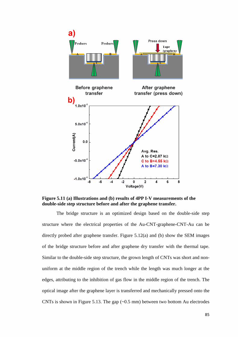
85
Figure 5.11 (a) Illustrations and (b) results of 4PP I-V measurements of the
double-side step structure before and after the graphene transfer.
The bridge structure is an optimized design based on the double-side step
structure where the electrical properties of the Au-CNT-graphene-CNT-Au can be
directly probed after graphene transfer. Figure 5.12(a) and (b) show the SEM images
of the bridge structure before and after graphene dry transfer with the thermal tape.
Similar to the double-side step structure, the grown length of CNTs was short and non-
uniform at the middle region of the trench while the length was much longer at the
edges, attributing to the inhibition of gas flow in the middle region of the trench. The
optical image after the graphene layer is transferred and mechanically pressed onto the
CNTs is shown in Figure 5.13. The gap (~0.5 mm) between two bottom Au electrodes

86
with CNTs grown on the top can be observed, suggesting that no shortage is present
between two bottom Au electrodes (or two CNT bundles). The illustrations and results
of 4PP I-V measurements of the bridge structure before and after graphene transfer
were shown in Figure 5.14(a) and (b). After graphene transfer, the structure shows a
linear response to the current when the voltage sweep (-1 to 1V) was applied. However,
since the free-standing CNTs grown in the trench was too short, similar to the double-
side step structure, the collapse of CNTs may also happen, leading to the shortage
between the graphene and the bottom Au electrodes. The measured total resistance
shows a small value (174Ω) since the large contact resistances between the transferred
graphene and Au electrodes were omitted in the bridge structure. However, the actual
contact area between the transferred graphene and CNTs was still unknown due to the
existing air-gap between the transferred graphene and CNTs, as shown in Figure 5.13.
Besides, to isolate the resistance of one CNT bump (𝑅𝐴𝑢−𝐶𝑁𝑇−𝐺 ) from the total
resistance, the graphene resistance needs to be estimated. Further optimization of the
bridge structure will be described in Chapter 6.
Figure 5.12 SEM images of the bridge structure (a) before and (b) after graphene
dry transfer with the thermal tape.
87
Figure 5.13 Optical image of the bridge structure after the graphene layer
transferred and pressed down on to the CNTs.
Figure 5.14 (a) Illustrations and (b) results of 4PP I-V measurements of the
bridge structure before and after the graphene transfer.

88
5.6 Summary
In this chapter, the process of transferring a top-graphene layer onto the CNTs
was explored and the electrical properties of the fabricated structures were studied.
Using the bridge structure and graphene dry transfer with a thermal tape, the electrical
properties of the Au-CNT-graphene-CNT-Au structure can be directly probed. The
electrical characterization shows a linear response to the current when the voltage
sweep (-1 to 1V) was applied after graphene transferred. At the same time, the total
resistance of Au-CNT-graphene-CNT-Au was calculated as 174Ω. The optimization of
the bridge structure is required to further investigate the electrical properties of direct
graphene-to-CNT contact.

89
Chapter 6 : Electrical Properties of Direct Graphene-to-CNT Contact
6.1 Introduction
In Chapter 5, the process of transferring a top-graphene layer onto the CNTs
using the bridge structure, and graphene dry transfer with a thermal tape has been
explored. However, further process improvement is required due to some remaining
issues. (1) The shortage between the graphene and the bottom Au electrodes was still
possible as the free-standing CNTs grown in the trench was too short, making CNTs
susceptible to collision upon graphene transfer and mechanical pressing. (2) The actual
contact area between the transferred graphene and CNTs was still unknown due to the
presence of an air-gap between the transferred graphene and CNTs. (3) The graphene
resistance needs to be estimated to isolate the resistance of one CNT bump
(𝑅𝐴𝑢−𝐶𝑁𝑇−𝐺) from the total resistance of the bridge structure.
6.2 Experimental Objective and Scope
This chapter aims to improve the bridge structure and graphene transferring
process to further investigate the electrical properties of direct graphene-to-CNT
contact. The resistance of one CNT bump (𝑅𝐴𝑢−𝐶𝑁𝑇−𝐺), including the CNT/graphene
contact resistance, will be extracted from the total resistance of the graphene bridge
structure to benchmark with the 𝑅𝐴𝑢−𝐶𝑁𝑇−𝐴𝑢 , which include the CNT/Au contact
resistance in the Au bridge structure. The resistance of one CNT bump (𝑅𝐴𝑢−𝐶𝑁𝑇−𝐺)
will be compared with the state-of-the-art studies on similar work.
6.3 Design and Fabrication of the Graphene Bridge Structure
Major fabrication and assembly steps of the Au-CNT-graphene-CNT-Au
structure are summarized in Figure 6.1. The fabrication uses Si substrate with 280 nm
SiO2 layer deposited using thermal oxidation technique (Figure 6.1, step 1). First,
bottom Au pads (20nm Ti/100nm Au) and buffer/catalyst layer (8nm Al/2nm

90
Al2O3/1.1nm Fe) were sequentially patterned on a silicon wafer using e-beam
evaporation deposition and lift-off process (Figure 6.1, step 2). Then, free-standing
CNTs were grown using thermal chemical vapour deposition (TCVD) method with
hydrogen (H2) and acetylene (C2H2) gas flow ratio of 3:1 at 650˚C (Figure 6.1, step 3).
After CNT growth, two pieces of 80μm thickness polyethylene terephthalate (PET)
with double-side non-conducting adhesives were assembled on the sides of CNT
bundles as the spacers to support the free-standing CNTs when the top graphene layer
was transferred (Figure 6.1, step 4). Finally, few-layer graphene on PET (or SiO2/Si)
substrate was flipped over and pressed down onto the CNT bundles (Figure 6.1, step
5). Graphene with the substrate was attached by the mechanical force of the top
adhesive of PET spacers, creating direct contact between the graphene and CNTs
(Figure 6.1, step 6).
Figure 6.1 Fabrication and assembly steps of the Au-CNT-graphene-CNT-Au
structure.

91
6.4 Electrical Characterization Method
The high contact resistance between CNTs and metal is always a key obstacle
in limiting their feasibility in the CNT interconnect application [51]. However,
significant discrepancies are present in the state-of-the-art values of CNT/metal
contact resistance, and there are no standard processes for the estimation. Different
groups presented their results with various measurement techniques and assumptions
on various samples. In this work, Au film (with SiO2/Si substrate) replaced the
graphene layer as the control sample when CNT growth conditions and assembly
processes remained to be identical. Four-point-probe (4PP) I-V measurements
(Keithley 4200-SCS Semiconductor Characterization System) were used to
characterize the electrical properties of the graphene and Au bridge structure. The total
resistance of the graphene and Au bridge structure can be expressed as:
𝑅𝑡𝑜𝑡𝑎𝑙 = 𝑅𝑏𝑡𝑚_𝐴𝑢 + 2𝑅𝐴𝑢−𝐶𝑁𝑇−𝐺 + 𝑅𝐺 (1)
and
𝑅𝑡𝑜𝑡𝑎𝑙 = 𝑅𝑏𝑡𝑚_𝐴𝑢 + 2𝑅𝐴𝑢−𝐶𝑁𝑇−𝐴𝑢 + 𝑅𝑡𝑜𝑝_𝐴𝑢 (2), correspondingly,
where 𝑅𝑏𝑡𝑚_𝐴𝑢 is the resistance of bottom Au pads; 𝑅𝐴𝑢−𝐶𝑁𝑇−𝐺 and 𝑅𝐴𝑢−𝐶𝑁𝑇−𝐴𝑢 are
the resistance of one CNT bump including the contact resistance of CNT/bottom Au,
the resistance of bulk CNT and the contact resistance of CNT/graphene or CNT/top
Au; 𝑅𝐺 and 𝑅𝑡𝑜𝑝_𝐴𝑢 are the resistance of top graphene layer and Au film,
correspondingly.
To extract the 𝑅𝐴𝑢−𝐶𝑁𝑇−𝐺 and 𝑅𝐴𝑢−𝐶𝑁𝑇−𝐴𝑢 in Equation (1) and (2), the values
of 𝑅𝑏𝑡𝑚_𝐴𝑢, 𝑅𝐺 and 𝑅𝑡𝑜𝑝_𝐴𝑢 need to be determined. 𝑅𝑏𝑡𝑚_𝐴𝑢 can be measured from the
control groups with the same dimension of bottom Au pads. 𝑅𝐺 and 𝑅𝑡𝑜𝑝_𝐴𝑢 can be
estimated using the equation of R =𝐿
𝑊𝑒𝑓𝑓𝑅𝑆 (3), where L is the distance between two

92
CNT bundles; 𝑊𝑒𝑓𝑓 is the effective width of top graphene layer or Au film; 𝑅𝑆 is the
sheet resistance of the graphene layer or Au film. Nevertheless, to utilize Eq. (1) and
(2), CNT resistance needs to be subtracted. Using the reported CNT resistivity of 9.7
to 33.8 mΩ•cm [51], [53], CNT resistance can be determined using Ohm’s law.
However, the calculation is carried out based on the assumptions where the current
density distribution and the crystallinity across the whole CNT bundles are similar. In
actual CNT growth, discrepancies in crystallinity and current density across various
regions of CNT bundles can be anticipated. Nevertheless, in this work, the overall
electrical properties of CNT bundles are taken into consideration to explore the
feasibility of CNT-graphene heterostructure in TSV interconnect applications.
6.5 Results and Discussion
Graphene samples on substrate used in this chapter were intrinsic CVD
graphene transferred on the top of PET (or 350nm SiO2/Si wafer) with a dimension of
10mm × 10mm. The structural characteristics of graphene were confirmed by optical
microscopy and Raman characterization as 1-3 layers poly-crystal graphene (Figure
6.2). On the other hand, 20nm Ti/100nm Au was deposited by e-beam evaporator on
280nm SiO2/Si wafer to be used as the control samples to benchmark against the
graphene samples. The sheet resistances of graphene layer and Au film were in a range
of 218-237 and 0.31-0.32 Ω/sq, respectively, measured by 4PP sheet resistance
measurement machine. Large sheet resistance of graphene may be attributed to the
grain boundaries of poly-crystal formed during the CVD growth, and the defects or
deformations induced from the transfer process of micro-scale area onto the substrate.
Based on Equation (3), 𝑅𝐺 will be ~730 times larger than 𝑅𝑡𝑜𝑝_𝐴𝑢 with the same
dimension (L/𝑊𝑒𝑓𝑓), leading to a significant increase of the total resistance of the
graphene bridge structure. To reduce the effect of 𝑅𝐺 , another configuration of CNT

93
area (Figure 6.3, configuration A) with much smaller distance (L) between two CNT
bundles was designed as a comparison to the regular square-shaped CNT area Figure
6.3, configuration B). The size of CNT area in configuration A and B was maintained
at the same value.
Figure 6.2 (a) Optical and (b) Raman images of the graphene on SiO2/Si and PET.

94
Figure 6.3 Schematic diagrams and SEM images of two configurations of CNT
area with the same size (left: configuration A, right: configuration B).
Optical microscopy (OM) and scanning electron microscopy (SEM) images of
the fabricated Au-CNT-graphene-CNT-Au structure of configuration A are presented
in Figure 6.4. As shown in Figure 6.4(a) and (b), two uniform, well-aligned CNT walls
were grown on the top of bottom Au pads. Figure 6.4(c) and (d) show the direct
contact of poly-crystal graphene with the observable grain boundaries to the CNTs.
Meanwhile, a dummy sample in the same batch with the real sample after CNT growth
was sliced to observe the cross-section view of two CNT walls in SEM, as shown in
Figure 6.4(e) and (f). The vertical length of CNTs was controlled by the growth time
to be slightly higher than the thickness of PET spacers (80 μm).

95
Figure 6.4 (a) and (b) SEM images after CNT growth; (c) and (d) optical images
after top graphene layer transferred; (e) and (f) SEM cross-section view of two
CNT walls of the dummy sample cut in half.
The vertical length of CNT walls on the dummy sample was directly measured
from the cross-section SEM image as shown in Figure 6.5(a). The planar length of
CNT walls on the same dummy sample measured from the tilted-view SEM was
shown in Figure 6.5(b). From the tilted-view SEM image, the planar length of CNT
walls on the real sample was measured (Figure 6.6) with good uniformity. Using the
same ratio of the planar and vertical length of CNTs on the dummy sample, the
vertical length of CNT walls on the real sample can be calculated to be 110 μm as
shown in Table 6.1. The IG/ID peak ratio and average diameter of the CNTs was ~1.5
and ~3 nm correspondingly as shown in Figure 6.7(a) and (b). CNT density was
estimated to be ~1011 cm-2, which is expectedly tmuch higher than PECVD grown
CNTs (~109 cm-2) [126].

96
Figure 6.5 (a) Cross-section SEM image of the vertical length of CNT walls on the
dummy sample and (b) the planar length of CNT walls on the same dummy
sample from the top-view SEM image tilted at 20˚.
Figure 6.6 The planar length of CNT walls on the real sample from the top-view
SEM image tilted at 20˚.
Table 6.1 The vertical and planar length of CNT walls on the dummy sample and
real sample.
Sample Vertical length
(μm)
Planar length
(μm)
Ratio of the
planar and
vertical length
Dummy
sample
154 52 0.34
Real sample 110 (calculated) 37 0.34
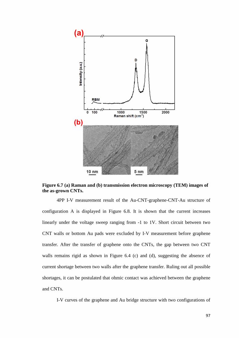
97
Figure 6.7 (a) Raman and (b) transmission electron microscopy (TEM) images of
the as-grown CNTs.
4PP I-V measurement result of the Au-CNT-graphene-CNT-Au structure of
configuration A is displayed in Figure 6.8. It is shown that the current increases
linearly under the voltage sweep ranging from -1 to 1V. Short circuit between two
CNT walls or bottom Au pads were excluded by I-V measurement before graphene
transfer. After the transfer of graphene onto the CNTs, the gap between two CNT
walls remains rigid as shown in Figure 6.4 (c) and (d), suggesting the absence of
current shortage between two walls after the graphene transfer. Ruling out all possible
shortages, it can be postulated that ohmic contact was achieved between the graphene
and CNTs.
I-V curves of the graphene and Au bridge structure with two configurations of

98
CNT area are shown in Figure 6.8. The Au bridge structure shows a linear response to
the current when the voltage is applied, similar to its graphene bridge counterpart.
However, its total resistance was smaller compared to the value of the graphene bridge
structure with the same configuration of CNT area. It is mainly because 𝑅𝐺 was much
larger than 𝑅𝑡𝑜𝑝_𝐴𝑢 as explained above. Meanwhile, for the graphene bridge structure,
configuration A (30μm×3mm) with closer distance (L) between two CNT walls had
much smaller total resistance than the value of configuration B (300μm×300μm) as
expected also due to the large 𝑅𝐺 in configuration B. Figure 6.9 shows the SEM
images of cross-section view of the graphene bridge structure (SiO2/Si) with CNT area
in configuration B, indicating that there was no shortage between the graphene and the
bottom Au pads.
Figure 6.8 4pp I-V measurement results of the total resistance of the graphene
and Au bridge structure with two configurations of CNT area.

99
Figure 6.9 SEM images of cross-section view of the graphene bridge structure
(SiO2/Si substrate) with CNT area in configuration B.
The measured values of 𝑅𝑏𝑡𝑚_𝐴𝑢 and estimated values of 𝑅𝐺 and 𝑅𝑡𝑜𝑝_𝐴𝑢 for
various CNT area and graphene layer dimensions are listed in Table 6.3. 𝑅𝐺 and
𝑅𝑡𝑜𝑝_𝐴𝑢 can be estimated using the Equation (3): R =𝐿
𝑊𝑒𝑓𝑓𝑅𝑆 , where L is the distance
between two CNT bundles; 𝑊𝑒𝑓𝑓 is the effective width of top graphene layer or Au
film; 𝑅𝑆 is the sheet resistance of the graphene layer or Au film. Based on two
configurations of CNT area and the physical width (W) of the graphene layer or Au
film, as shown in Figure 6.3 and Table 6.3, we can conclude that
1) For the CNT area with configuration A, 𝑊𝑒𝑓𝑓 ≈ W since the width b of CNT
area (3mm) is close to W (3.6 or 4.5mm) and the L (80μm) is much smaller
compared to the value of b (3mm);
2) For the CNT area with configuration B, 𝑊𝑒𝑓𝑓 < W since the width b of CNT
area (300μm) is much smaller than W (4.2 or 3.4mm) and the L (770 or 610μm)
is larger than the value of b (300μm).
For the CNT area with configuration B, 𝑊𝑒𝑓𝑓 can be determined by transfer
length method (TLM) with two Cu electrodes replacing the two CNT bundles on the
top of Au film with sample size of 5mm × 10mm, as shown in Figure 6.10. The total
resistance between two Cu electrodes can be expressed as

100
𝑅𝑡𝑜𝑡𝑎𝑙 = 2(𝑅𝐶𝑢/𝐴𝑢 + 𝑅𝐶𝑢) +𝑅𝑆
𝑊𝑒𝑓𝑓𝐿𝐶𝑢 ,
where 𝑅𝐶𝑢/𝐴𝑢 and 𝑅𝐶𝑢 are the contact resistance between Cu and Au and the bulk
resistance of one Cu electrode, correspondingly; 𝑅𝑆 is the sheet resistance of Au film;
𝐿𝐶𝑢 is the distance between two Cu electrodes. By varying the distance between two
Cu electrodes, the total resistance vs. 𝐿𝐶𝑢 will have a linear response. The slope equals
to 𝑅𝑆/𝑊𝑒𝑓𝑓.
Figure 6.11 shows the optical images of patterned two Cu electrodes on the Au
film with three different values of 𝐿𝐶𝑢. Table 6.2 shows the 4PP I-V measured total
resistances of different 𝐿𝐶𝑢 from three batches of samples. Figure 6.12 plots the linear
response of the total resistance vs. 𝐿𝐶𝑢 with a slope of 194.3 mΩ/mm. 𝑅𝑆 of Au film
was measured to be 313 mΩ by 4PP sheet resistance measurement machine.
Subsequently, 𝑊𝑒𝑓𝑓 was calculated to be 1.6 mm (applicable for L within the range of
396-794 μm).
Figure 6.10 Illustration of two Cu electrodes replacing the two CNT bundles on
the top of Au film.

101
Figure 6.11 Optical images of patterned two Cu electrodes on the Au film with
three different values of 𝑳𝑪𝒖
Figure 6.12 The linear response of the total resistance vs. L_Cu.
Table 6.2 4PP I-V measured total resistances of different 𝑳𝑪𝒖 from three batches
of samples.
𝐿𝐶𝑢 (mm) Resistance (mΩ)
Batch 1 Batch 2 Batch 3
0.396 104 113 113
0.594 154 156 152
0.794 186 190 193

102
Table 6.3 Total and extracted one CNT bump resistance of the graphene and Au
bridge structure with two configurations of CNT area.
Configuration W
(mm) L
(mm)
CNT area 𝑹𝒕𝒐𝒕𝒂𝒍
(Ω)
𝑹𝒃𝒕𝒎_𝑨𝒖 (Ω)
𝑹𝒕𝒐𝒑_𝑨𝒖
(Ω)
𝑹𝑮
(Ω)
𝑹𝑨𝒖−𝑪𝑵𝑻−𝑮
or
𝑹𝑨𝒖−𝑪𝑵𝑻−𝑨𝒖
(Ω) a
(mm) b
(mm) S
(𝑚𝑚2)
A with graphene
bridge (PET) 3.6 0.08 0.03 2.95 0.09 10.0 0.7 / 5.1 2.1
A with Au bridge (SiO
2/Si) 4.5 0.08 0.03 2.96 0.09 5.2 0.7 0.01 / 2.2
B with graphene bridge (SiO
2/Si) 4.2 0.77 0.28 0.28 0.08 128.1 7.0 / 110.7 5.2
B with Au bridge (SiO
2/Si) 3.4 0.61 0.30 0.30 0.09 18.2 7.0 0.12 / 5.5
𝑅𝐴𝑢−𝐶𝑁𝑇−𝐺 and 𝑅𝐴𝑢−𝐶𝑁𝑇−𝐴𝑢 are extracted from Equation (1) and (2) as shown
in Table 6.3. Under the same configuration, 𝑅𝐴𝑢−𝐶𝑁𝑇−𝐺 was similar to 𝑅𝐴𝑢−𝐶𝑁𝑇−𝐴𝑢
suggesting that similar contact was formed at the CNT/graphene interface and at the
CNT/top Au interface. The contact between CNTs and graphene can be possibly
achieved by the Van der Waals forces as the current density ( ≪108 A/cm2) induced
from I-V measurements is relatively insignificant to fuse the CNTs and graphene with
covalent carbon bonds [127]. On the other hand, the contact resistance between CNTs
and graphene was slightly smaller than the contact resistance between CNTs and Au.
A possible reason for this can be attributed to the work function of graphene (4.6eV)
which is closer to the value of CNTs (4.7~4.9eV at sidewalls, at tips it will be smaller
[128]) as compared to Au (5.1eV), where the electron tunnelling was affected by the
work function difference in this case. Under the identical CNT area, the contact
resistances between CNTs and graphene (or between CNTs and Au) of configuration
A and B were different. This shows that a non-uniform current density exists at the
CNT/graphene (or CNT/Au) contact due to the current crowding effect [129]. The
effective contact area of configuration A is larger than configuration B resulting in
smaller contact resistance in configuration A. The Ohmic contact obtained aligns well

103
with the assumptions in using Eq. (1) and (2), as mentioned in the previous section. As
Ohmic contact can be postulated, the contact resistance can be postulated to increase
linearly with reduced contact area, as agreed by Ohm’s law. In other words, a possible
increase in contact resistance may be anticipated for miniaturized interconnects with
smaller CNT-graphene contact area. However, in actual CNT-graphene interconnects,
more uncertainties shall be considered, such as discrepancies in CNT
height/crystallinity across CNTs, which requires further investigations to address these
possible discrepancies.
The resistance of one CNT bump (𝑅𝐴𝑢−𝐶𝑁𝑇−𝐺) in this work is compared with
the results from the state-of-the-art as shown in Table 6.4. With simple normalization
of the CNT area, it shows that our result compares favourably with the literatures
[130], [131]. However, as the reported studies used various CNT area dimensions,
further study is needed to explore the possible factors affecting the CNT/graphene
contact resistance.
Table 6.4 Resistance of one CNT bump (including the CNT/metal (CNT/graphene)
contact resistance) of this work and the reported state-of-the-art.
𝑅𝐴𝑢−𝐶𝑁𝑇−𝐴𝑢
[130] 𝑅𝑍𝑟𝑁−𝐶𝑁𝑇−𝐴𝑙
[131] 𝑅𝐴𝑢−𝐶𝑁𝑇−𝐴𝑢
[51] 𝑅𝐴𝑢−𝐶𝑁𝑇−𝐺
(this work)
CNT bump
resistance
R (Ω)
280 457 16.1 2.1
CNT area
(µm2)
1963 2827 7854 90000
CNT height
(µm) 120 300 132 110
Repeatability tests of the total resistance were conducted to each graphene and
Au bridge structure as shown in Table 6.5. Except for the graphene bridge structure
with PET substrate, other three structures with SiO2/Si substrate show increasing trend
in resistances under repeated voltage sweep (-1 to 1V). This can be attributed to the

104
damage of accumulating charges at the air gap between CNTs and graphene (or Au)
contact. However, for the graphene bridge structure with PET substrate, the air gap
can be shortened by the electrostatic force of accumulating charges after several
voltage sweeps since the PET substrate is flexible. Thus, the total resistance of
graphene bridge structure with PET substrate decreases initially, and then stabilized at
the lowest value under repeated voltage sweep.
Table 6.5 Repeatability tests of the total resistance for the graphene and Au
bridge structures.
Sample 𝑹𝒕𝒐𝒕𝒂𝒍 (Ω)
1st 2
nd 3
rd 4
th 5
th
A with graphene
bridge (PET) 11.1 10.6 10.0 10.2 10.0
A with Au bridge
(SiO2/Si)
5.2 6.2 7.0 6.8 7.0
B with graphene
bridge (SiO2/Si)
128.1 135.4 135.0 135.0 133.7
B with Au bridge
(SiO2/Si)
18.2 21.3 21.8 22.3 23.3
6.6 Summary
In this chapter, transfer process of a top graphene layer onto the as-grown CNT
bundles was improved. Direct graphene-to-CNT contact was formed at the
CNT/graphene interface. 4PP I-V characterization suggests that an ohmic contact was
achieved between the graphene and CNTs. Low CNT bump resistance of 2.1Ω for
90,000 µm2 CNT area including the CNT/graphene contact resistance was obtained,
demonstrating reduction of contact resistance between CNT and Au under the same
fabrication and measurement conditions. This chapter presents the preliminary results
for the assembly process of top-transferred graphene on CNTs and the electrical
properties of the direct CNT/graphene contact.

105
Chapter 7 : Femtosecond Laser Annealing for Graphene-CNT Fusion
7.1 Introduction
In Chapter 6, we fabricated the graphene bridge structure with the direct
graphene-to-CNT contact. Mechanical pressing is used to enhance the CNT-graphene
bonding. Next, annealing methods are explored for graphene and CNTs fusion, to
form carbon covalent bonds which can further decrease the contact resistance and
enhance the reliability. Three annealing methods, i.e. thermal annealing, electric-
current-induced Joule heating and laser annealing, were proposed for graphene-CNT
fusion. For the bridge structure in Chapter 6, thermal annealing may not be applicable
as our preliminary results show that the global heating of the whole sample piece at a
high temperature (>400˚C) will burn the PET spacers and destroy the bridge structure.
For the method of electric-current-induced Joule heating, as discussed in Chapter 6,
the current density which can be induced by probing in our Keithley 4200-SCS
Semiconductor Characterization System is too small (≪108 A/cm2) to fuse the CNTs
and graphene. Thus, laser annealing may be the most suitable method for the fusion
trials on the graphene bridge structure.
7.2 Experimental Objective and Scope
Femtosecond laser irradiation can induce intense, localised annealing which is
highly controllable and repeatable. This chapter aims to explore the conditions of
femtosecond laser annealing for the fusion of graphene and CNTs in the bridge
structure. First, the laser power was fine-tuned to generate optimized Joule heat on the
graphene/CNT interface without damaging the CNT/graphene. After optimizing the
laser power, laser annealing will be applied on the graphene bridge sample.
7.3 Femtosecond Laser Power Tuning
In this work, a Ti-Sapphire COHERENT Ultra II femtosecond laser was used.

106
The beam wavelength was set at 800 nm. The pulse duration was 140 fs with a
repetition rate of 80 MHz. The laser beam was focused with a 10x microscope
objective resulting in an effective laser spot diameter of ~10 μm.
Before the laser annealing of the graphene bridge sample, the laser power was
tuned to an optimized value to generate optimized Joule heat on the graphene/CNT
interface without damaging the CNT/graphene. A dummy bridge structure sample
with graphene (with PET substrate) transferred onto CNTs was used for laser power
tuning. Figure 7.1(a) shows the illustration of the laser beam focus position on the
graphene/CNT interface while Figure 7.1(b) shows the burned marks of power tuning
results. From the laser power values summarized in Table 7.1, it can be observed that
any single-spot mode laser with power above 0.0166W would result in burning of
CNTs, as shown in Figure 7.1(b). For the laser line scanning mode, the Joule heat
generated by the laser beam was lower than the single spot with the same power
(0.0394W). Nevertheless, a burned mark (G) can still be observed after the line
scanning.
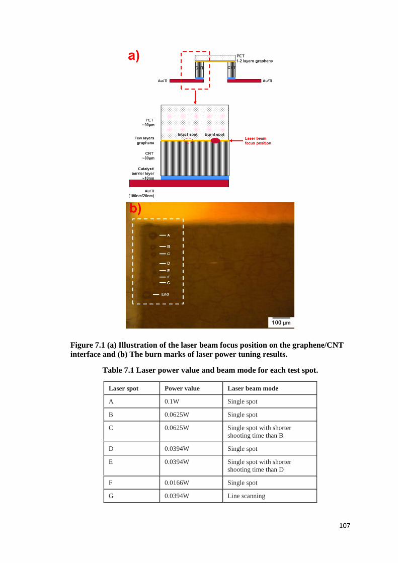
107
Figure 7.1 (a) Illustration of the laser beam focus position on the graphene/CNT
interface and (b) The burn marks of laser power tuning results.
Table 7.1 Laser power value and beam mode for each test spot.
Laser spot Power value Laser beam mode
A 0.1W Single spot
B 0.0625W Single spot
C 0.0625W Single spot with shorter
shooting time than B
D 0.0394W Single spot
E 0.0394W Single spot with shorter
shooting time than D
F 0.0166W Single spot
G 0.0394W Line scanning

108
7.4 Results and Discussion
After the laser power tuning, 0.0166W was selected as the optimized value for
annealing. A fresh piece of bridge structure sample with graphene (with PET substrate)
transferred onto the same CNT area as configuration A in Chapter 6 was used for the
laser annealing trials. Figure 7.2 shows the illustration of laser line scanning approach.
Since the width of CNT wall was 30 μm and the laser spot diameter was ~10 μm, 3
line scans (top + middle + bottom) for each CNT wall were carried out and the line
scan length was fixed at 3 mm, covering the full length of each CNT wall. 4PP I-V
measurements were used to characterize the electrical properties of the graphene
bridge sample before and after laser annealing. From the results shown in Table 7.2, it
can be observed that the total resistance of graphene bridge sample without annealing
decreases initially when applying voltage sweep (-1 to 1V), From the 3rd sweep
onwards, the total resistance increases after the repeated voltage sweep (-1 to 1V).
After the first laser annealing, the total resistance dropped to the lowest value (27.3 Ω)
but increased after the second and third laser annealing. Figure 7.3 shows the
comparison of the I-V curves before and after 1st laser annealing, showing the
decreasing of the total resistance upon laser annealing. However, it does not give
sufficient evidences to conclude that the resistance dropping was due to the fusion of
graphene and CNTs by the laser annealing as the resistance values before and after
laser annealing did not exhibit much consistency and stability. The resistance after 1st
laser annealing (27.3 Ω) was still close to the 3rd sweep without laser annealing (29.1
Ω). Another possibility in decrease in resistance may attributed to the air-gap
shortened by the electrostatic force of accumulating charges after voltage stressing,
which is not solely contributed by the fusion of graphene and CNTs after laser
annealing.

109
Figure 7.4 shows the comparison of the graphene bridge sample after the laser
annealing and graphene-on-CNT sample (discussed in Chapter 6) without laser
annealing. The burned marks observed from the laser annealing sample indicating that
after the 3rd laser scanning the sample was already over annealed, which partially
explained the increase in resistance of graphene bridge structure after the 3rd laser
annealing as shown in Table 7.2.
Figure 7.2 Illustration of 3 laser line scans covered the full length of one CNT
wall.
-0.8 -0.6 -0.4 -0.2 0.0 0.2 0.4 0.6 0.8-0.04
-0.03
-0.02
-0.01
0.00
0.01
0.02
0.03
0.04
Cu
rren
t(A
)
Voltage(V)
Before graphene transfer
Before laser annealing (35.0)
After laser annealing (27.3)
Figure 7.3 Comparison of the I-V curves before and after 1st laser annealing.

110
Figure 7.4 Comparison of (a) the graphene bridge sample through the laser
annealing and (b) graphene-on-CNT sample (discussed in Chapter 6).
Table 7.2 Resistances of the graphene bridge structure before and after laser
annealing.
𝑹𝒕𝒐𝒕𝒂𝒍 (Ω)
Before laser annealing After laser annealing
1st 2
nd 3
rd 4
th 5
th 1
st laser
annealing 2
nd laser
annealing 3
rd laser
annealing
43.8 32.1 29.1 37.4 35.0 27.3 28.1 29.0
7.5 Summary
In this chapter, the conditions of femtosecond laser annealing for the fusion of
graphene and CNTs in the bridge structure were explored. After the laser power tuning,
0.0166W was selected as the optimized value for annealing. Laser line scanning was
applied at the graphene/CNT interface and the electrical properties of the pristine
graphene bridge and annealed graphene bridge samples were characterized. The total
resistance of the bridge structure dropped to its lowest (27.3 Ω) after the first laser
scanning, but increased after the second and third laser annealing. However, the
obtained outcomes give insufficient evidences to conclude that the resistance dropping
was due to the fusion of graphene and CNTs by the laser annealing. Therefore, further
studies are needed to verify the formation of CNT-graphene bonding its impact on the
overall resistance upon laser annealing.

111
Chapter 8 : Conclusion and Future Work
8.1 Conclusion
In this study, development and optimization of CNT-graphene heterostructure
were carried out for its application in TSV interconnects. First, recipes and
methodology to grow free-standing CNTs on graphene sheet were optimized. CNTs
grown with TCVD technique yield sufficient length (~334μm) and density (~1011 cm-2)
for its application in TSV interconnects. Different growth parameters such as catalyst
film thickness, growth time and growth temperature were systemically studied. With
the understanding of different growth parameters, the feasibility in growing CNTs
within TSVs on the bottom graphene electrodes can be explored.
After the development and growth of free standing CNTs, fabrication process
flow of graphene-CNT heterostructure within TSVs was designed and explored. TSV
fabrication was successfully demonstrated using lithography and DRIE techniques.
Catalyst layer and graphene layer were also deposited onto the bottom wafer to
accommodate latter growth of CNTs within the TSVs on top of the graphene layer.
However, as compared to the free-standing growth of CNTs on the graphene, CNTs
grown within the unfilled TSVs are relatively sparse owing to the process-engineering
steps involved. Therefore, suitable process optimization and improvement steps have
been carried out to improve the density of CNTs grown within TSVs.
After demonstration of CNT growth within TSVs on top of graphene layer, the
process of transferring a top-graphene layer onto the CNTs was explored. At the same
time, the electrical properties of the fabricated structures were studied. Using the
bridge structure and graphene dry transfer with a thermal tape, the electrical properties
of the Au-CNT-graphene-CNT-Au structure can be directly probed. The electrical
characterization shows a linear response to the current when the voltage sweep (-1 to

112
1V) was applied after graphene transferred. At the same time, the total resistance of
Au-CNT-graphene-CNT-Au was calculated as 174Ω. The optimization of the bridge
structure is required to further investigate the electrical properties of direct graphene-
to-CNT contact.
To improve the electrical properties and reduce the contact resistance at the
graphene-CNT interface, mechanical pressing was applied onto the structure. At the
same time, graphene bridge structure was developed and fabricated to better
characterize the electrical properties of the CNT/graphene interface. Direct graphene-
to-CNT contact was formed at the CNT/graphene interface. 4PP I-V characterization
suggests that an ohmic contact was achieved between the graphene and CNTs. Low
CNT bump resistance of 2.1Ω for 90,000 µm2 CNT area including the CNT/graphene
contact resistance was obtained, demonstrating reduction of contact resistance between
CNT and Au under the same fabrication and measurement conditions.
In conclusion, this work demonstrates the feasibility of CNT-graphene
heterostructure for its application in TSV interconnects. Various possible technical
difficulties have been addressed and explored: (1) CNTs of sufficient height (~334μm)
and density (~1011 cm-2) is grown for TSV interconnect application, (2) CNTs are
successfully grown in fabricated TSVs on top of the graphene layer, (3) Graphene
bridge structure is developed to improve the electrical characterization steps of CNT-
graphene heterostructure, (4) Contact resistance between CNT-graphene is reduced by
mechanical pressing. The outcomes from this research provide significant insights in
the understanding of CNT-graphene heterostructure for TSV interconnect application,
which paves the way for the latter researches in optimization and commercialization of
CNT-graphene interconnects.
113
8.2 Future Work
In this thesis, development of CNT-graphene heterostructure for TSV
interconnect applications has been demonstrated. CNTs with top/bottom graphene
layers have been grown and assembled in pre-fabricated TSVs for full-carbon,
miniaturized interconnect application. Various technical challenges have been
addressed, such as difficulties in electrical properties characterizations, and contact
resistance in CNT-graphene interface. For further realization of CNT-graphene
heterostructure for TSV interconnect applications, the following studies and
development work can be carried out.
In Chapter 4, CNT obtained within the unfilled TSV was sparse, with relatively
few CNTs grown per unit area as compared to free-standing CNT bundles. This can be
attributed to the process-engineering steps involved in wafer-bonding, grinding and
wet/dry etching. At the same time, the high aspect ratio (5~10) of the TSVs may
hinder the flow of carbon precursors into the bottom of the TSV pits during Thermal
Chemical Vapor Deposition (TCVD) process, which result in sparsely-grown CNTs.
Hence, process steps of TSV fabrication and conditions for CNT growth need to be
modified and optimized in order to obtain higher CNT fillings within the TSVs. At the
same time, the TCVD recipe for CNT growth can be further fine-tuned, to ensure
smooth flow of carbon precursor into the TSV pits during TCVD process.
Despite demonstration of reduced contact resistance within CNT-graphene
interface and approximate calculation of contact resistance value, the exact
relationship between the contact resistance and the contact area of graphene and CNTs
is still unclear. Theoretically, for interconnects with larger area, the electron mobility
will be higher, hence result in higher electrical conductivity. However, an opposing
postulation may bring up where the presence of larger contact area results in larger

114
CNT-graphene electron barrier, hindering the flow of electrons through the interface.
As this study demonstrates the calculation and deduction of contact resistance between
CNT-graphene, it serves as a preliminary step for future studies where the relationship
between contact resistance and the contact area of graphene-CNTs can be determined.
Therefore, more experimental work can be conducted in order to quantify the contact
resistance with the certain contact area.
In this work, low CNT bump resistance of 2.1Ω for 90,000 µm2 CNT area
including the CNT/graphene contact resistance was obtained. This suggests the
reduction of contact resistance upon mechanical pressing technique. However, the
CNT area fabricated in this work is 90,000 µm2 which is too large for the application
of CNT-graphene heterostructure for the state-of-the-art TSV interconnect applications.
Nevertheless, the reduction of contact resistance paved a useful path for future
miniaturization of the reported heterostructure. Combining the previous suggested
future work on studying the relationship between contact resistance and the CNT-
graphene contact area, the miniaturization of the CNT-graphene heterostructure can be
carried out smoothly. Therefore, further study will be conducted to narrow down the
CNT area and explore the possible factors affecting the CNT/graphene contact
resistance.
Fusion of CNT-graphene structures by forming covalent bonds within CNT-
graphene interface is important for further reduction of contact resistance and
increasing the mechanical reliability of CNT-graphene heterostructure. In Chapter 7,
the treatment of CNT-graphene heterostructure using femtosecond laser has been
demonstrated. From the obtained electrical characterizations, it can be deduced that
femtosecond laser treatment reduces the contact resistance in CNT-graphene interface,
where this reduction can be attributed to the fusion of CNT/graphene interface.
115
Despite demonstration of reduced resistance upon femtosecond laser treatment, the
fusion effect of femtosecond laser on CNT-graphene heterostructure remained
unexplored. Therefore, fusion of the graphene and CNTs with carbon covalent bonds
needs to be further studied.
Heat-dissipation and cooling issues are aggravated in 3-D ICs due to presence
of different interfaces with widely-differing thermal and electrical conductivities,
creating bottlenecks to facile heat transfer from chip to chip. Hotspots across various
layers in chip-stacks severely degrade overall system performance, leading to critical
and random device failures, and elevated temperatures severely affect carrier-mobility,
and threshold voltages of the transistors. Different solutions have therefore been
proposed to alleviate the thermal congestion, ranging from algorithmic approaches (i.e.,
thermal floorplanning and thermal TSV placement) to micro-fluidic channels. As an
alternative, the integration of highly thermally conductive materials, e.g. CNT and
graphene is one of the strongly promising ways to overcome the thermal bottlenecks.
Since CNT and graphene possess high thermal-conductivity (1767 W/mK for CNT
bundles and 1300 W/mK for multi-layer graphene, compared to copper’s 400 W/mK
and tungsten’s 175 W/mK), the 3-D interconnects based on CNT-graphene
heterostructure are supposed to remove the hot spots faster than traditional metals.
Therefore, thermal property of the full carbon-based 3-D interconnects with CNT-
graphene heterostructure is required to be further studied.
Another challenge topic for 3-D interconnects is the application for high
frequency devices, where the traditional metals e.g. Cu or Au have the skin depth
issues adversely leading to signal losses at high frequencies beyond 100 GHz. As one
of the advantages, the large kinetic inductance and negligible magnetic inductance
allow CNT to have a negligible skin depth effect. The integration of CNT and

116
graphene with seamless carbon covalent bonds can help to extend this advantage to
three dimensions compared with the metal counterparts. Thus, high-frequency
characterization of the full carbon-based 3-D interconnects with CNT-graphene
heterostructure needs to be performed for future work in order to explore the possible
applications in high-frequency electronic devices.

117
Author’s Publication
During doctor’s work
1) Ye Zhu, Chong Wei Tan, Shen Lin Chua, Yu Dian Lim, Boris Vaisband, Beng Kang
Tay, Eby G. Friedman, Chuan Seng Tan, “Assembly Process and Electrical Properties
of Top-Transferred Graphene on Carbon Nanotubes for Carbon-Based Three-
Dimensional Interconnects”, Components Packaging and Manufacturing Technology
IEEE Transactions on, DOI: 10.1109/TCPMT.2019.2940511.
2) Chong Wei Tan, Ye Zhu, Shen Lin Chua, Maziar Shakerzadeh, Chuan Seng Tan and B
eng Kang Tay, “Electrical properties of FCVA deposited nano-crystalline graphitic
carbon thin films with in-situ treatment techniques”, Eur. Phys. J. Appl. Phys., 85,
20301 (2019). DOI: 10.1051/epjap/2019180097
3) Ye Zhu, Chong Wei Tan, Shen Lin Chua, Yu Dian Lim, Beng Kang Tay, Chuan Seng
Tan, “Growth and Fabrication of Carbon-Based Three-Dimensional Heterostructure in
Through-Silicon Vias (TSVs) for 3D Interconnects”, IEEE 19th Electronics Packaging
Technology Conference (EPTC), 2017, pp. 1-5.
Pre-doctor’s work
4) Ye Zhu, Kaushik Ghosh, Hong Yu Li, Yiheng Lin, Chuan Seng Tan, Guangrui
(Maggie) Xia, “On the Origins of Near-Surface Stresses in Silicon around Cu-filled and
CNT-filled Through Silicon Vias”, Semiconductor Science and Technology, vol. 31,
2016, p. 055008.
5) Ye Zhu, Jiye Zhang, Hong Yu Li, Chuan Seng Tan and Guangrui (Maggie) Xia,
“Study of Near-surface Stresses in Silicon around Through Silicon Vias at Elevated
Temperatures by Raman Spectroscopy and Simulations.” IEEE Transactions on Device
and Materials Reliability, vol. 15, 2015, pp.142-148.

118
References
[1] E. C. Niehenke, “Wireless communications: Present and future: Introduction to
focused issue articles,” IEEE Microw. Mag., vol. 15, no. 2, pp. 26–35, 2014.
[2] H. N. Khan, D. A. Hounshell, and E. R. H. Fuchs, “Science and research policy
at the end of Moore’s law,” Nat. Electron., vol. 1, no. 1, pp. 14–21, 2018.
[3] A. Pizzagalli, “Lithography technology and trends for More than Moore
devices: advanced packaging and MEMS devices,” Proc. SPIE, vol. 10775, no.
September 2018, pp. 1–3, 2018.
[4] K. Palem and A. Lingamneni, “What to Do About the End of Moore’s Law,
Probably!,” Dac 2012, pp. 1–6, 2012.
[5] R. R. Schaller, “MOORE ’ S LAW : past , present , future,” IEEE Spectr., vol.
34, no. 6, pp. 52–59, 1997.
[6] H. Iwai, “End of the scaling theory and Moore’s law,” 2016 16th Int. Work.
Junction Technol., pp. 1–4, 2016.
[7] WikiHow, “10 nm lithography process,” Semiconductor and Computer
Engineering, 2019. [Online]. Available:
https://en.wikichip.org/wiki/10_nm_lithography_process. [Accessed: 05-Aug-
2019].
[8] J. Horwitz, “TSMC speeds up 5-nanometer chip manufacturing process due to
5G demand,” Venture Beat, 19-Jul-2019.
[9] J. Hruska, “TSMC Announces First EUV 7nm Risk Production, 5nm Tapeouts
in Q2 2019,” Extreme Tech, 12-Oct-2018.
[10] D. Bishop, “Nanotechnology and the end of Moore’s Law?,” Bell Syst. Tech. J.,
vol. 10, no. 3, pp. 23–28, 2005.
[11] A. A. Chien and V. Karamcheti, “Moore’s law: The first ending and a new

119
beginning,” Computer (Long. Beach. Calif)., vol. 46, no. 12, pp. 48–53, 2013.
[12] R. R. Tummala, “Moore’s Law meets its match,” IEEE Spectr., vol. 43, no. 6,
pp. 44–49, 2006.
[13] B. Li, T. D. Sullivan, T. C. Lee, and D. Badami, “Reliability challenges for
copper interconnects,” Microelectron. Reliab., vol. 44, no. 3, pp. 365–380,
2004.
[14] X. Li, T. K. S. Wong, Rusli, and D. Yang, “Structural and electronic properties
of low dielectric constant carbon rich amorphous silicon carbide,” Diam. Relat.
Mater., vol. 12, no. 3–7, pp. 963–967, 2003.
[15] L. G. Gosset et al., “Integration of SiOC air gaps in copper interconnects,”
Microelectron. Eng., vol. 70, no. 2–4, pp. 274–279, 2003.
[16] M. T. Bohr, “Interconnect scaling-the real limiter to high performance ULSI,”
Int. Electron Devices Meet., pp. 241–244, 1995.
[17] S. K. Ryu, K. H. Lu, X. Zhang, J. Im, P. S. Ho, and R. Huang,
“Thermomechanical reliability challenges for 3D interconnects with through-
silicon vias,” AIP Conf. Proc., vol. 1300, no. 2010, pp. 189–201, 2010.
[18] H. Treichel, G. Ruhl, P. Ansmann, R. Würl, C. Müller, and M. Dietlmeier,
“Low dielectric constant materials for interlayer dielectric (Invited paper),”
Microelectron. Eng., vol. 40, no. 1, pp. 1–19, 1998.
[19] H. Zhou, F. G. Shi, B. Zhao, and J. Yota, “Effect of deposition methods on
dielectric breakdown strength of PECVD low-k carbon doped silicon dioxide
dielectric thin films,” Microelectronics J., vol. 35, no. 7, pp. 571–576, 2004.
[20] G. Bomchil, A. Halimaoui, and R. Herino, “Porous Silicon: The Material and its
Applications in Silicon-on-Insulator Technologies,” Appl. Surf. Sci., vol. 42, pp.
604–613, 1988.
120
[21] F. Gaillard et al., “Chemical etching solutions for air gap formation using a
sacrificial oxide/polymer approach,” Microelectron. Eng., vol. 83, no. 11–12,
pp. 2309–2313, 2006.
[22] J. Noguchi et al., “Process and reliability of air-gap Cu interconnect using 90-
nm node technology,” IEEE Trans. Electron Devices, vol. 52, no. 3, pp. 352–
359, 2005.
[23] S. Q. Gu et al., “Stackable memory of 3D chip integration for mobile
applications,” Tech. Dig. - Int. Electron Devices Meet. IEDM, no. 858, pp. 3–6,
2008.
[24] L. P, “what is 3d ic integration and what metrology is needed,” in Conference
on Frontiers of Characterization and Metrology for Nanoelectronics, 2007.
[25] S. Das, A. Chandrakasan, and R. Reif, “Timing, energy, and thermal
performance of three-dimensional integrated circuits,” in Proc. Great Lakes
Symposum on VLSI, 2004, p. 338.
[26] H. P. Hofstee, “Future microprocessors and off-chip SOP interconnect,” IEEE
Trans. Adv. Packag., vol. 27, no. 2, pp. 301–303, 2004.
[27] E. Beyne, “The rise of the 3rd dimension for system intergration,” in
International Interconnect Technology Conference, IITC, 2006, pp. 1–5.
[28] C. C. Yap et al., “Carbon nanotube bumps for the flip chip packaging system.,”
Nanoscale Res. Lett., vol. 7, no. 1, p. 105, 2012.
[29] T. Wang et al., “Through-silicon vias filled with densified and transferred
carbon nanotube forests,” IEEE Electron Device Lett., vol. 33, no. 3, pp. 420–
422, 2012.
[30] S. Vollebregt, S. Banerjee, F. D. Tichelaar, and R. Ishihara, “The growth of
carbon nanotubes on electrically conductive ZrN support layers for through-

121
silicon vias,” Microelectron. Eng., vol. 156, pp. 126–130, 2015.
[31] H. Tong, “Microelectronics packaging present and future,” Mater. Chem. Phys.,
vol. 40, pp. 147–161, 1995.
[32] J. H. Lau, “Overview and outlook of through-silicon via (TSV) and 3D
integrations,” Microelectron. Int., vol. 28, no. 2, pp. 8–22, 2011.
[33] T. Jiang, S. K. Ryu, Q. Zhao, J. Im, R. Huang, and P. S. Ho, “Measurement and
analysis of thermal stresses in 3D integrated structures containing through-
silicon-vias,” Microelectron. Reliab., vol. 53, no. 1, pp. 53–62, 2013.
[34] Y. Y. Wu, Y. L. Chen, and C. C. Lee, “Solid state bonding of silicon chips to
copper substrates using silver with cavities,” J. Mater. Sci. Mater. Electron.,
vol. 27, no. 4, pp. 3347–3354, 2016.
[35] P. Bayat et al., “Thermo-mechanical characterization of copper through-silicon
vias (Cu-TSVs) using micro-Raman spectroscopy and atomic force
microscopy,” Microelectron. Eng., vol. 137, no. 1, pp. 101–104, 2015.
[36] N. Ranganathan, K. Prasad, N. Balasubramanian, and K. L. Pey, “A study of
thermo-mechanical stress and its impact on through-silicon vias,” J.
Micromechanics Microengineering, vol. 18, no. 7, 2008.
[37] C. S. Selvanayagam, J. H. Lau, X. Zhang, S. K. W. Seah, K. Vaidyanathan, and
C. T. C, “Nonlinear thermal stress/strain analyses of copper filled TSV (through
silicon via) and their flip-chip microbumps,” IEEE Trans. Adv. Packag., vol.
32, no. 4, pp. 1073–1081, 2008.
[38] K. H. Lu, X. Zhang, S. K. Ryu, J. Im, R. Huang, and P. S. Ho, “Thermo-
mechanical reliability of 3-D ICs containing through silicon vias,” Proc. -
Electron. Components Technol. Conf., pp. 630–634, 2009.
[39] K. H. Lu et al., “Thermal stress induced delamination of through silicon vias in

122
3-D interconnects,” Proc. - Electron. Components Technol. Conf., pp. 40–45,
2010.
[40] S. K. Ryu, K. H. Lu, X. Zhang, J. H. Im, P. S. Ho, and R. Huang, “Impact of
near-surface thermal stresses on interfacial reliability of through-silicon vias for
3-D Interconnects,” IEEE Trans. Device Mater. Reliab., vol. 11, no. 1, pp. 35–
43, 2011.
[41] Scott E. Thompson, Guangyu Sun, Youn Sung Choi, and Toshikazu Nishida,
“Uniaxial-Process-Induced Strained-Si: Extending the CMOS Roadmap,” IEEE
Trans. Electron Devices, vol. 53, no. 5, pp. 1010–1020, 2006.
[42] A. P. Karmarkar, X. Xu, and V. Moroz, “Performanace and reliability analysis
of 3D-integration structures employing through silicon via (TSV),” IEEE Int.
Reliab. Phys. Symp. Proc., pp. 682–687, 2009.
[43] S. Cho, “Technical Challenges in TSV Integration,” Online, 2011. [Online].
Available:
http://www.internationalsematech.com/meetings/archives/symposia/10202/Sess
ion 2-3D TSV/3D_Samsung.pdf.
[44] K. Athikulwongse, A. Chakraborty, J. S. Yangt, D. Z. Pan, and S. K. Lim,
“Stress-driven 3D-IC placement with TSV keep-out zone and regularity study,”
IEEE/ACM Int. Conf. Comput. Des. Dig. Tech. Pap. ICCAD, pp. 669–674,
2010.
[45] V. Re, L. Gaioni, A. Manazza, M. Manghisoni, L. Ratti, and G. Traversi,
“Radiation tolerance of devices and circuits in a 3D technology based on the
vertical integration of two 130-nm CMOS layers,” IEEE Trans. Nucl. Sci., vol.
60, no. 6, pp. 4526–4532, 2013.
[46] L. Di Cioccio et al., “(Invited) Low Temperature Direct Bonding 3D Stacking

123
Technologies for High Density Device Integration,” ECS Trans., vol. 58, no. 9,
pp. 17–28, 2013.
[47] B.-J. Lwo, K.-H. Tseng, and K.-F. Tseng, “A Study on Electrical Reliability
Criterion on Through Silicon Via Packaging,” J. Electron. Packag., vol. 138,
no. 2, p. 024501, 2016.
[48] X. Zhong et al., “Process development of a stacked chip module with TSV
interconnection,” ICEPT-HDP 2012 Proc. - 2012 13th Int. Conf. Electron.
Packag. Technol. High Density Packag., pp. 8–11, 2012.
[49] Y. Li, Y. Sun, and J. T. W. Yeow, “Nanotube field electron emission:
principles, development, and applications,” Nanotechnology, vol. 26, no. 24, p.
242001, 2015.
[50] D. Tan et al., “Improved RF Isolation Using Carbon Nanotube Fence-Wall for
3-D Integrated Circuits and Packaging,” IEEE Microw. Wirel. Components
Lett., vol. 25, no. 6, pp. 355–357, 2015.
[51] T. Wang, K. Jeppson, L. Ye, and J. Liu, “Carbon-nanotube through-silicon via
interconnects for three-dimensional integration,” Small, vol. 7, no. 16, pp.
2313–2317, 2011.
[52] H. J. Dai, E. W. Wong, and C. M. Lieber, “Probing Electrical Transport in
Nanomaterials: Conductivity of Individual Carbon Nanotubes,” Science (80-. ).,
vol. 272, no. 5261, pp. 523–526, 1996.
[53] T. Xu, Z. Wang, J. Miao, X. Chen, and C. M. Tan, “Aligned carbon nanotubes
for through-wafer interconnects,” Appl. Phys. Lett., vol. 91, no. 4, pp. 79–82,
2007.
[54] T. Wang et al., “Through-silicon vias filled with densified and transferred
carbon nanotube forests,” IEEE Electron Device Lett., vol. 33, no. 3, pp. 420–

124
422, 2012.
[55] B. Q. Wei, R. Vajtai, and P. M. Ajayan, “Reliability and current carrying
capacity of carbon nanotubes,” Appl. Phys. Lett., vol. 79, no. 8, pp. 1172–1174,
2001.
[56] P. Kim, L. Shi, A. Majumdar, and P. L. McEuen, “Thermal transport
measurements of individual multiwalled nanotubes,” Phys. Rev. Lett., vol. 87,
no. 21, pp. 215502-1-215502–4, 2001.
[57] T. Y. Choi, D. Poulikakos, J. Tharian, and U. Sennhauser, “Measurement of
thermal conductivity of individual multiwalled carbon nanotubes by the 3-ω
method,” Appl. Phys. Lett., vol. 87, no. 1, pp. 1–3, 2005.
[58] J. W. Jiang, J. S. Wang, and B. Li, “Thermal expansion in single-walled carbon
nanotubes and graphene: Nonequilibrium Green’s function approach,” Phys.
Rev. B - Condens. Matter Mater. Phys., vol. 80, no. 20, pp. 1–7, 2009.
[59] Y. Zhu, J. Zhang, H. Y. Li, C. S. Tan, and G. Xia, “Study of near-surface
stresses in silicon around through-silicon vias at elevated temperatures by
Raman spectroscopy and simulations,” IEEE Trans. Device Mater. Reliab., vol.
15, no. 2, pp. 142–148, 2015.
[60] S. Vollebregt, R. Ishihara, F. Tichelaar, J. Van Der Cingel, and K. Beenakker,
“Electrical characterization of carbon nanotube vertical interconnects with
different lengths and widths,” 2012 IEEE Int. Interconnect Technol. Conf. IITC
2012, pp. 1–3, 2012.
[61] J. Vanpaemel et al., “Growth and integration challenges for carbon nanotube
interconnects,” Microelectron. Eng., vol. 120, pp. 188–193, 2014.
[62] N. Chiodarelli et al., “Integration of Vertical Carbon Nanotube Bundles for
Interconnects,” J. Electrochem. Soc., vol. 157, no. 10, p. K211, 2010.

125
[63] I. Soga et al., “Carbon nanotube bumps for LSI interconnect,” Proc. - Electron.
Components Technol. Conf., pp. 1390–1394, 2008.
[64] S. Hermann, B. Pahl, R. Ecke, S. E. Schulz, and T. Gessner, “Carbon nanotubes
for nanoscale low temperature flip chip connections,” Microelectron. Eng., vol.
87, no. 3, pp. 438–442, 2010.
[65] T. Iwai, H. Shioya, D. Kondo, S. Hirose, and A. Kawabata, “Thermal and
source bumps utilizing carbon nanotubes for flip-chip high power amplifiers,”
in IEEE International Electron Devices Meeting, 2005, pp. 257–260.
[66] C. Xu, H. Li, and K. Banerjee, “Modeling, analysis, and design of graphene
nano-ribbon interconnects,” IEEE Trans. Electron Devices, vol. 56, no. 8, pp.
1567–1578, 2009.
[67] H. Li, C. Xu, N. Srivastava, and K. Banerjee, “Carbon Nanomaterials for Next-
Generation Interconnects and Passives: Physics, Status, and Prospects,” IEEE
Trans. Electron Devices, vol. 56, no. 9, pp. 1799–1821, 2009.
[68] D. Sarkar, C. Xu, H. Li, and K. Banerjee, “High-frequency behavior of
graphene-based interconnects-Part I: Impedance modeling,” IEEE Trans.
Electron Devices, vol. 58, no. 3, pp. 843–852, 2011.
[69] D. Sarkar, C. Xu, H. Li, and K. Banerjee, “High-frequency behavior of
graphene-based interconnect-sPart II: Impedance analysis and implications for
inductor design,” IEEE Trans. Electron Devices, vol. 58, no. 3, pp. 853–859,
2011.
[70] A. Sinha, J. A. Mihailovic, J. E. Morris, H. Lu, and C. Bailey, “Modeling
thermal conductivity and CTE for CNT-Cu composites for 3-D TSV
application,” 2010 IEEE Nanotechnol. Mater. Devices Conf. NMDC2010, pp.
262–266, 2010.

126
[71] W. S. Zhao, Y. F. Liu, Z. Yong, Y. Fang, and W. Y. Yin, “Modeling and
characterization of carbon-based heterogeneous interconnects for 3-D ICs,”
EDAPS 2013 - 2013 IEEE Electr. Des. Adv. Packag. Syst. Symp., pp. 154–157,
2013.
[72] D. K. Georgios, T. Emmanuel, F. E. George, G. Maroulis, and T. E. Simos,
“Pillared Graphene: A New 3-D Innovative Network Nanostructure Augments
Hydrogen Storage,” Nano Lett., vol. 8, no. 10, pp. 3166–3170, 2009.
[73] Y. S. Kim, K. Kumar, F. T. Fisher, and E. H. Yang, “Out-of-plane growth of
CNTs on graphene for supercapacitor applications,” Nanotechnology, vol. 23,
no. 1, pp. 0–7, 2012.
[74] L. Xu, N. Wei, Y. Zheng, Z. Fan, H. Q. Wang, and J. C. Zheng, “Graphene-
nanotube 3D networks: Intriguing thermal and mechanical properties,” J.
Mater. Chem., vol. 22, no. 4, pp. 1435–1444, 2012.
[75] P. Architectures, V. Varshney, S. S. Patnaik, A. K. Roy, G. Froudakis, and B. L.
Farmer, “Modeling of Thermal Transport in,” ACS Nano, vol. 4, no. 2, pp.
1153–1161, 2010.
[76] J. Y. Jhan, Y. W. Huang, C. H. Hsu, H. Teng, D. Kuo, and P. L. Kuo, “Three-
dimensional network of graphene grown with carbon nanotubes as carbon
support for fuel cells,” Energy, vol. 53, pp. 282–287, 2013.
[77] D. Yu and L. Dai, “Self-assembled graphene/carbon nanotube hybrid films for
supercapacitors,” J. Phys. Chem. Lett., vol. 1, no. 2, pp. 467–470, 2010.
[78] F. Du, D. Yu, L. Dai, S. Ganguli, V. Varshney, and A. K. Roy, “Preparation of
tunable 3D pillared carbon nanotube-graphene networks for high-performance
capacitance,” Chem. Mater., vol. 23, no. 21, pp. 4810–4816, 2011.
[79] F. D. Novaes, R. Rurali, and P. Ordejón, “Electronic transport between

127
graphene layers covalently connected by carbon nanotubes,” ACS Nano, vol. 4,
no. 12, pp. 7596–7602, 2010.
[80] W. Zhang et al., “Synthesis of three-dimensional carbon nanotube/graphene
hybrid materials by a two-step chemical vapor deposition process,” Carbon N.
Y., vol. 86, pp. 358–362, 2015.
[81] Z. Fan et al., “A three-dimensional carbon nanotube/graphene sandwich and its
application as electrode in supercapacitors,” Adv. Mater., vol. 22, no. 33, pp.
3723–3728, 2010.
[82] L. L. Zhang, Z. Xiong, and X. S. Zhao, “Pillaring Chemically Exfoliated
Graphene Oxide with CNT for Photocatalytic Degradation of Dyes under
Visible Light Irradiation (SWNT).pdf,” ACS Nano, vol. 4, no. 11, pp. 7030–
7036, 2010.
[83] D. H. Lee et al., “Versatile carbon hybrid films composed of vertical carbon
nanotubes crown on mechanically compliant graphene films,” Adv. Mater., vol.
22, no. 11, pp. 1247–1252, 2010.
[84] Y. Zhu et al., “A seamless three-dimensional carbon nanotube graphene hybrid
material,” Nat. Commun., vol. 3, no. 92, pp. 1225–1227, 2012.
[85] D. Kondo, S. Sato, and Y. Awano, “Self-organization of novel carbon
composite structure: Graphene multi-layers combined perpendicularly with
aligned carbon nanotubes,” Appl. Phys. Express, vol. 1, no. 7, pp. 0740031–
0740033, 2008.
[86] S. F. Al-sarawi, D. Abbott, and P. D. Franzon, “A review of 3-D packaging
technology,” IEEE Trans. Components Packag. Manuf. Technol. Part B, vol.
21, no. 1, pp. 2–14, 1998.
[87] M. Karnezos, “3D packaging: where all technologies come together,” in

128
International Electronics Manufacturing Technology Symposium, 2004, pp. 64–
67.
[88] R. Maltiel, “Semiconductor Experts, Witnesses, Consultants and Patent
Litigation Support,” Online, 2013. [Online]. Available:
http://semiconductorexpert.blogspot.ca/2013/01/tsmc-and-globalfoundries-3-
d.html.
[89] J. Van Olmen et al., “3D stacked IC demonstrator using hybrid collective die-
to-wafer bonding with copper through silicon vias (TSV),” 2009 IEEE Int.
Conf. 3D Syst. Integr. 3DIC 2009, pp. 1–5, 2009.
[90] T. Fukushima et al., “New three-dimensional integration technology based on
reconfigured wafer-on-wafer bonding technique,” Tech. Dig. - Int. Electron
Devices Meet. IEDM, vol. 3, no. 6, pp. 985–988, 2007.
[91] S. Pargfrieder, P. Kettner, M. Privett, and J. Ting, “Temporary Bonding and
DeBonding Enabling TSV Formation and 3D Integration for Ultra-thin
Wafers,” in Electronics Packaging Technology Conference, 2008, pp. 1301–
1305.
[92] M. Puech, N. Launay, N. Arnal, P. Godinat, A. Micro, and M. Systems,
“Fabrication of 3D packaging TSV using DRIE,” in Symposium on Design,
Test, Integration and Packaging of MEMS/MOEMS, 2008, pp. 109–114.
[93] V. F. Pavlidis and E. G. Friedman, “Interconnect-based design methodologies
for three-dimensional integrated circuits,” Proc. IEEE, vol. 97, no. 1, pp. 123–
140, 2009.
[94] M. J. Wolf et al., “High aspect ratio TSV copper filling with different seed
layers,” Proc. - Electron. Components Technol. Conf., pp. 563–570, 2008.
[95] S. Sandireddy and T. Jiang, “Advanced wafer thinning technologies to enable

129
multichip packages,” 2005 IEEE Work. Microelectron. Electron Devices,
WMED, vol. 2005, pp. 24–27, 2005.
[96] S. W. Yoon, D. W. Yang, J. H. Koo, M. Padmanathan, and F. Carson, “3D TSV
processes and its assembly/packaging technology,” 2009 IEEE Int. Conf. 3D
Syst. Integr. 3DIC 2009, pp. 1–5, 2009.
[97] M. Motoyoshi, “Through-Silicon Via (TSV),” in Proceedings of the IEEE,
2009, pp. 43–48.
[98] N. Khan et al., “Development of 3-D silicon module with TSV for system in
packaging,” IEEE Trans. Components Packag. Technol., vol. 33, no. 1, pp. 3–9,
2010.
[99] Z. Chen, X. Song, and S. Liu, “Thermo-mechanical characterization of copper
filled and polymer filled TSVs considering nonlinear material behaviors,” Proc.
- Electron. Components Technol. Conf., pp. 1374–1380, 2009.
[100] P. B. Chinoy and J. Tajadod, “Processing and Microwave Characterization of
Multilevel Interconnects Using Benzocyclobutene Dielectric,” IEEE Trans.
Components, Hybrids, Manuf. Technol., vol. 16, no. 7, pp. 714–719, 1993.
[101] J. Yannou, “3D IC and TSV interconnects 2010,” Online, 2010. [Online].
Available: http://www.slideshare.net/Yole_Developpement.
[102] R. Xie et al., “Carbon nanotube growth for through silicon via application,”
Nanotechnology, vol. 24, no. 12, 2013.
[103] Y. Fu, Y. Qin, T. Wang, S. Chen, and J. Liu, “Ultrafast transfer of metal-
enhanced carbon nanotubes at low temperature for large-scale electronics
assembly,” Adv. Mater., vol. 22, no. 44, pp. 5039–5042, 2010.
[104] S. H. Han et al., “Contact resistance between Au and solution-processed CNT,”
Solid. State. Electron., vol. 54, no. 5, pp. 586–589, 2010.

130
[105] H. Xu, L. Chen, L. Hu, and N. Zhitenev, “Contact resistance of flexible,
transparent carbon nanotube films with metals,” Appl. Phys. Lett., vol. 97, no.
14, 2010.
[106] S. C. Lim et al., “Contact resistance between metal and carbon nanotube
interconnects: Effect of work function and wettability,” Appl. Phys. Lett., vol.
95, no. 26, pp. 93–96, 2009.
[107] M. H. Moaiyeri and F. Razi, “Performance analysis and enhancement of 10-nm
GAA CNTFET-based circuits in the presence of CNT-metal contact resistance,”
J. Comput. Electron., vol. 16, no. 2, pp. 240–252, 2017.
[108] S. E. Lee, K. S. Moon, and Y. Sohn, “Temperature dependence of contact
resistance at metal/MWNT interface,” Appl. Phys. Lett., vol. 109, no. 2, 2016.
[109] R. Hafizi, J. Tersoff, and V. Perebeinos, “Band Structure and Contact
Resistance of Carbon Nanotubes Deformed by a Metal Contact,” Phys. Rev.
Lett., vol. 119, no. 20, pp. 1–5, 2017.
[110] A. Fediai et al., “Impact of incomplete metal coverage on the electrical
properties of metal-CNT contacts: A large-scale ab initio study,” Appl. Phys.
Lett., vol. 109, no. 10, 2016.
[111] Y. Chai et al., “Low-resistance electrical contact to carbon nanotubes with
graphitic interfacial layer,” IEEE Trans. Electron Devices, vol. 59, no. 1, pp.
12–19, 2012.
[112] Y. Matsuda, W. Deng, and W. a G. Iii, “Quantum Mechanics Predictions for
Contact Resistance of ‘ End- contacted ’ Metal – Graphene and Metal –
Nanotube Interfaces,” J. Phys Chem. C, vol. 114, pp. 1–6, 2010.
[113] V. Labunov, B. Shulitski, A. Prudnikava, and A. Basaev, “Multi-level
composite nanostructures based on the arrays of vertically aligned carbon

131
nanotubes and planar graphite layers,” Phys. Status Solidi Appl. Mater. Sci., vol.
208, no. 2, pp. 453–458, 2011.
[114] K. Ghosh, N. Ranjan, Y. K. Verma, and C. S. Tan, “Graphene-CNT hetero-
structure for next generation interconnects,” RSC Adv., vol. 6, no. 58, pp.
53054–53061, 2016.
[115] J. Jiang, J. Kang, J. H. Chu, and K. Banerjee, “All-Carbon Interconnect Scheme
Integrating,” in International Electron Devices Meeting, 2017, pp. 342–345.
[116] L. Li, H. Li, Y. Guo, L. Yang, and Y. Fang, “Direct synthesis of
graphene/carbon nanotube hybrid films from multiwalled carbon nanotubes on
copper,” Carbon N. Y., vol. 118, pp. 675–679, 2017.
[117] R. Kotsilkova, I. Petrova-Doycheva, D. Menseidov, E. Ivanov, A. Paddubskaya,
and P. Kuzhir, “Exploring thermal annealing and graphene-carbon nanotube
additives to enhance crystallinity, thermal, electrical and tensile properties of
aged poly(lactic) acid-based filament for 3D printing,” Compos. Sci. Technol.,
vol. 181, no. May, p. 107712, 2019.
[118] W. B. Choi et al., “Aligned carbon nanotubes for nanoelectronics,”
Nanotechnology, vol. 15, no. 10, 2004.
[119] Y. Zhang, T. Ichihashi, E. Landree, F. Nihey, and S. Ijima, “Heterostructures of
Single-Walled Carbon Nanotubes and Carbide Nanorods,” Science (80-. )., vol.
285, p. 1719, 1999.
[120] J. W. Park, C. Park, J.-O. Lee, K.-H. Yoo, J. Kim, and J.-J. Kim, “Formation of
low-resistance ohmic contacts between carbon nanotube and metal electrodes
by a rapid thermal annealing method,” J. Phys. D. Appl. Phys., vol. 33, no. 16,
pp. 1953–1956, 2002.
[121] Y. Woo, G. S. Duesberg, and S. Roth, “Reduced contact resistance between an

132
individual single-walled carbon nanotube and a metal electrode by a local point
annealing,” Nanotechnology, vol. 18, no. 9, 2007.
[122] W. J. Baumgardner et al., “Pulsed laser annealing of thin films of self-
assembled nanocrystals,” ACS Nano, vol. 5, no. 9, pp. 7010–7019, 2011.
[123] D. Takagi, Y. Kobayashi, and H. Hibino, “Mechanism of Gold-Catalyzed
Carbon Material Growth,” Nano Lett., vol. 8, no. 3, pp. 832–835, 2008.
[124] Y. D. Lim, Q. Kong, S. Wang, C. W. Tan, B. K. Tay, and S. Aditya, “Enhanced
field emission properties of carbon nanotube films using densification
technique,” Appl. Surf. Sci., 2017.
[125] D. Tan et al., “A light-weight electromagnetic shield using high density carbon
nanotube fence-wall for RF packaging,” 2015 IEEE MTT-S Int. Microw. Symp.
IMS 2015, pp. 0–3, 2015.
[126] C. C. Yap, “DEVELOPMENT OF CARBON NANOTUBES FOR
INTERCONNECTS AND NANO-PACKAGING APPLICATIONS,” Nanyang
Technological University, 2013.
[127] K. Asaka, M. Karita, and Y. Saito, “Modification of interface structure and
contact resistance between a carbon nanotube and a gold electrode by local
melting,” Appl. Surf. Sci., vol. 257, no. 7, pp. 2850–2853, 2011.
[128] P. Liu et al., “Measuring the work function of carbon nanotubes with
thermionic method,” Nano Lett., vol. 8, no. 2, pp. 647–651, 2008.
[129] S. M. Song and B. J. Cho, “Contact resistance in graphene channel transistors,”
Carbon Lett., vol. 14, no. 3, pp. 162–170, 2013.
[130] T. Wang, K. Jeppson, N. Olofsson, E. E. B. Campbell, and J. Liu, “Through
silicon vias filled with planarized carbon nanotube bundles,” Nanotechnology,
vol. 20, no. 48, 2009.

133
[131] S. Vollebregt, S. Banerjee, F. D. Tichelaar, and R. Ishihara, “Carbon nanotubes
TSV grown on an electrically conductive ZrN support layer,” 2015 IEEE Int.
Interconnect Technol. Conf. 2015 IEEE Mater. Adv. Met. Conf. IITC/MAM
2015, pp. 281–283, 2015.