implementing a multi signal processing system for high ... a multi signal processing system for high...
TRANSCRIPT
Disclaimer: This document was part of the DSPSolution Challenge 1995 European Team Papers. Itmay have been written by someone whose nativelanguage is not English. TI assumes no liability for thequality of writing and/or the accuracy of theinformation contained herein.
Implementing a Multi Signal ProcessingSystem for High Speed Monitoring ofFACTS-Equipment in Electrical PowerSystems Using the TMS320C50 DSP
Authors: G. Herold, J. Ph. Jager, C.A. Weindl, A.v.Grafenstein, G. Schmid, C.K. Wehrfritz
EFRIE, FranceDecember 1995SPRA313
IMPORTANT NOTICE
Texas Instruments (TI) reserves the right to make changes to its products or to discontinue anysemiconductor product or service without notice, and advises its customers to obtain the latest version ofrelevant information to verify, before placing orders, that the information being relied on is current.
TI warrants performance of its semiconductor products and related software to the specifications applicableat the time of sale in accordance with TI’s standard warranty. Testing and other quality control techniquesare utilized to the extent TI deems necessary to support this warranty. Specific testing of all parameters ofeach device is not necessarily performed, except those mandated by government requirements.
Certain application using semiconductor products may involve potential risks of death, personal injury, orsevere property or environmental damage (“Critical Applications”).
TI SEMICONDUCTOR PRODUCTS ARE NOT DESIGNED, INTENDED, AUTHORIZED, OR WARRANTEDTO BE SUITABLE FOR USE IN LIFE-SUPPORT APPLICATIONS, DEVICES OR SYSTEMS OR OTHERCRITICAL APPLICATIONS.
Inclusion of TI products in such applications is understood to be fully at the risk of the customer. Use of TIproducts in such applications requires the written approval of an appropriate TI officer. Questions concerningpotential risk applications should be directed to TI through a local SC sales office.
In order to minimize risks associated with the customer’s applications, adequate design and operatingsafeguards should be provided by the customer to minimize inherent or procedural hazards.
TI assumes no liability for applications assistance, customer product design, software performance, orinfringement of patents or services described herein. Nor does TI warrant or represent that any license,either express or implied, is granted under any patent right, copyright, mask work right, or other intellectualproperty right of TI covering or relating to any combination, machine, or process in which suchsemiconductor products or services might be or are used.
Copyright © 1997, Texas Instruments Incorporated

TRADEMARKS
TI is a trademark of Texas Instruments Incorporated.
Other brands and names are the property of their respective owners.

CONTACT INFORMATION
US TMS320 HOTLINE (281) 274-2320
US TMS320 FAX (281) 274-2324
US TMS320 BBS (281) 274-2323
US TMS320 email [email protected]

ContentsAbstract ........................................................................................................................... 7Product Support on the World Wide Web .................................................................... 8Introduction..................................................................................................................... 9Description of the Network Online Monitoring System............................................. 11
Peripheral Components and Interfaces .................................................................... 11Structural Overview .......................................................................................... 11A/D Converter Systems .................................................................................... 12D/A Converter Systems .................................................................................... 13Keyboard/Display Interface............................................................................... 14
Multi-Signal Processing Architecture ........................................................................ 16Scalable Software Architecture................................................................................. 21
Test Environment and Results .................................................................................... 24Transient Network Analyzer Test Installation............................................................ 24Test Results.............................................................................................................. 24
Summary ....................................................................................................................... 28
FiguresFigure 1. Examples of FACTS Devices ............................................................................. 9Figure 2. Schematic Diagram of the Peripheral Components of the NOMS.................... 11Figure 3. Schematic Diagram of the A/D Converter Systems.......................................... 12Figure 4. Schematic Diagram of the D/A Converter System............................................ 14Figure 5. Schematic Diagram of the Keyboard/Display Interface .................................... 16Figure 6. Overview of the Central Processing Components............................................ 17Figure 7. Architecture of the DSP Unit............................................................................. 18Figure 8. Independent Request Bus Arbitration Method.................................................. 19Figure 9. Schematic Overview of the Multiprocessor Interface MPI ................................ 20Figure 10. Software Architecture of the NOMS (2 of 4 Nodes).......................................... 22Figure 11. TNS Test Installation ........................................................................................ 24Figure 12. Schematic Diagram of TNA Test Installation.................................................... 25Figure 13. Test Results of a 3-Phase Short Circuit (100 ms) ............................................ 26Figure 14. Test Results of a 3-Phase Short Circuit (1 s) ................................................... 27
Implementing a Multi Signal Processing System for High Speed Monitoring of 7FACTS-Equipment in Electrical Power Systems Using the TMS320C50 DSP
Implementing a Multi Signal ProcessingSystem for High Speed Monitoring of FACTS-
Equipment in Electrical Power SystemsUsing the TMS320C50 DSP
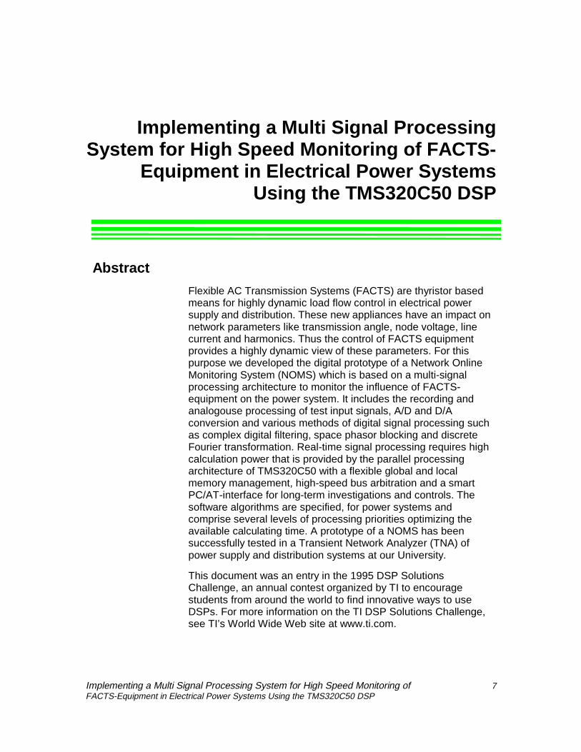
Abstract
Flexible AC Transmission Systems (FACTS) are thyristor basedmeans for highly dynamic load flow control in electrical powersupply and distribution. These new appliances have an impact onnetwork parameters like transmission angle, node voltage, linecurrent and harmonics. Thus the control of FACTS equipmentprovides a highly dynamic view of these parameters. For thispurpose we developed the digital prototype of a Network OnlineMonitoring System (NOMS) which is based on a multi-signalprocessing architecture to monitor the influence of FACTS-equipment on the power system. It includes the recording andanalogouse processing of test input signals, A/D and D/Aconversion and various methods of digital signal processing suchas complex digital filtering, space phasor blocking and discreteFourier transformation. Real-time signal processing requires highcalculation power that is provided by the parallel processingarchitecture of TMS320C50 with a flexible global and localmemory management, high-speed bus arbitration and a smartPC/AT-interface for long-term investigations and controls. Thesoftware algorithms are specified, for power systems andcomprise several levels of processing priorities optimizing theavailable calculating time. A prototype of a NOMS has beensuccessfully tested in a Transient Network Analyzer (TNA) ofpower supply and distribution systems at our University.
This document was an entry in the 1995 DSP SolutionsChallenge, an annual contest organized by TI to encouragestudents from around the world to find innovative ways to useDSPs. For more information on the TI DSP Solutions Challenge,see TI’s World Wide Web site at www.ti.com.

SPRA313
8 Implementing a Multi Signal Processing System for High Speed Monitoring ofFACTS-Equipment in Electrical Power Systems Using the TMS320C50 DSP
Product Support on the World Wide Web
Our World Wide Web site at www.ti.com contains the most up todate product information, revisions, and additions. Usersregistering with TI&ME can build custom information pages andreceive new product updates automatically via email.
SPRA313
Implementing a Multi Signal Processing System for High Speed Monitoring of 9FACTS-Equipment in Electrical Power Systems Using the TMS320C50 DSP
Introduction
To fulfil the increasing requirements of power supply anddistribution systems, the aspects of economy, reliability andquality are becoming more important. In modern public powernetworks of power supply the node voltage and line currentsignals are distorted or not sinusoidal at least. For example, thefollowing reasons can be stated:
q Application of modem FACTS-equipment for static varcompensation, transmission angle control and load flowdispatching.
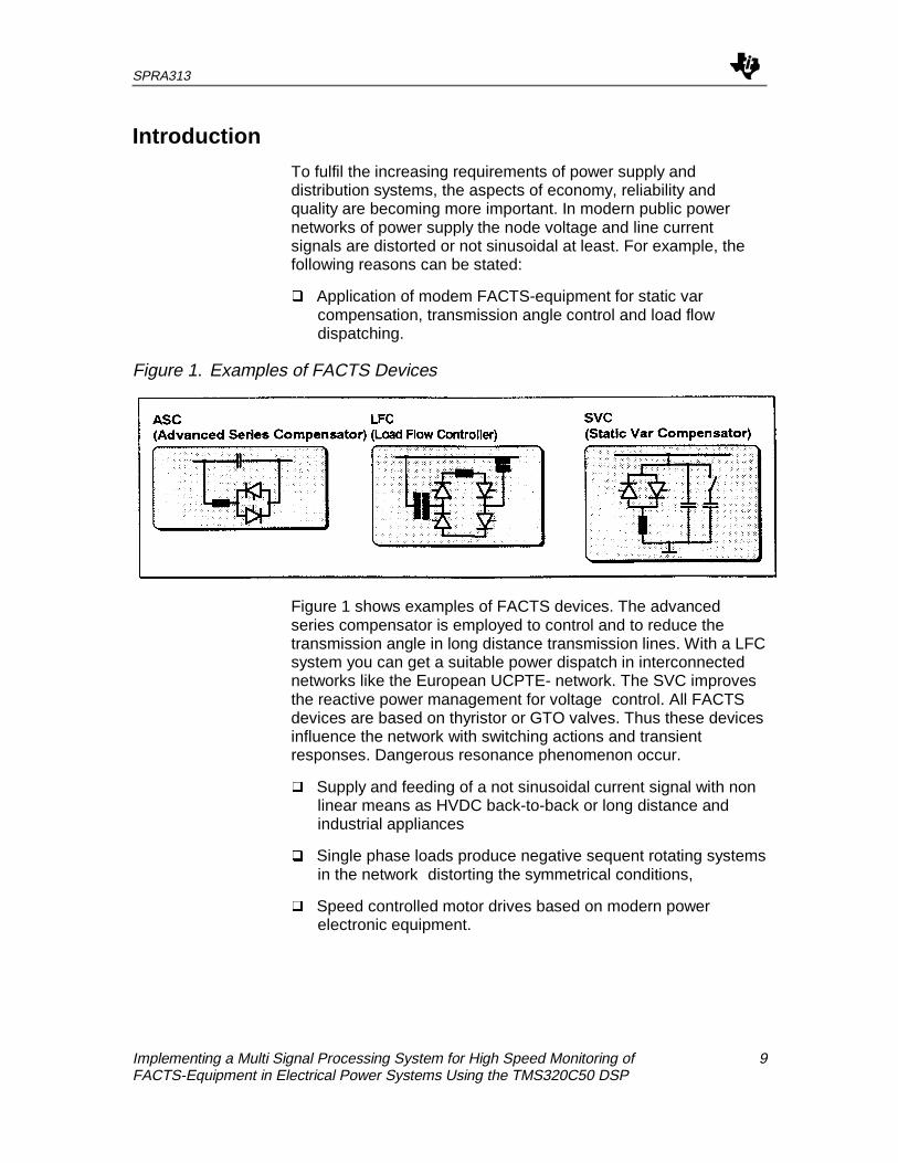
Figure 1. Examples of FACTS Devices
Figure 1 shows examples of FACTS devices. The advancedseries compensator is employed to control and to reduce thetransmission angle in long distance transmission lines. With a LFCsystem you can get a suitable power dispatch in interconnectednetworks like the European UCPTE- network. The SVC improvesthe reactive power management for voltage control. All FACTSdevices are based on thyristor or GTO valves. Thus these devicesinfluence the network with switching actions and transientresponses. Dangerous resonance phenomenon occur.
q Supply and feeding of a not sinusoidal current signal with nonlinear means as HVDC back-to-back or long distance andindustrial appliances
q Single phase loads produce negative sequent rotating systemsin the network distorting the symmetrical conditions,
q Speed controlled motor drives based on modern powerelectronic equipment.
SPRA313
10 Implementing a Multi Signal Processing System for High Speed Monitoring ofFACTS-Equipment in Electrical Power Systems Using the TMS320C50 DSP
The resulting transient responses, non-symmetrical conditions,flicker and harmonics produce interactions and instabilitiesreducing the quality and reliability of power systems considerably.The NOMS should record the distorted signals and analyze themto find a way to improve network conditions. There are many kindsof network distortions. Therefore, the NOMS must be based ondifferent test methods to investigate the network troubles.Following types of methods are necessary:
q Analysis of network harmonics and distortion with state phasorblocking
q Measurement of line power with complex phasors of themomentary power flow,
q Synchronous subtraction of absolute value and phase angle ofcomplex voltage phasors at several nodes in the network
q Selective acquisition of voltage and current values in a three-phase system
q On-line calculation of the network conditions
q On-line influencing and output of new parameters for theFACTS control
These features were taken into account developing the NOMS.The following chapters will show how these requirements wererealized with a prototype that is based on the digital signalprocessor TMS320C50. Especially in this process we haveattached importance to the accuracy of the hardware componentsand on-line calculations and furthermore to varied test methods.

SPRA313
Implementing a Multi Signal Processing System for High Speed Monitoring of 11FACTS-Equipment in Electrical Power Systems Using the TMS320C50 DSP
Description of the Network Online Monitoring System
Peripheral Components and Interfaces
Structural Overview
This chapter deals with the development, test and realization ofthe peripheral components of the NOMS. In this phase the maintask was to create the interface circuits between the high voltagenetwork and the control console and on the other hand side thesignalprocessing system. For this aim, high speed A/D-convertersystems for floating measurement of voltage and current statephasors and homopolar values are built up. The documentation ofthe test results was carried out with D/A-converter systems and aLCD-matrixdisplay. The on-line parameter control was managedby external keyboard system.
Figure 2. Schematic Diagram of the Peripheral Components of the NOMS
SPRA313
12 Implementing a Multi Signal Processing System for High Speed Monitoring ofFACTS-Equipment in Electrical Power Systems Using the TMS320C50 DSP
Figure 2 shows the schematic diagram of the peripheralcomponents of the NOMS. The DSP units are based on theTMS320C50 digital signal processor. Up to seven units can beprovided. To acquire the network information, there are up to eightavailable A/D-converters systems with active filtering for voltageand current acquisition. The PC-interface is used for datarecording of long-term investigations and will provide an additionalcapability for controlling the NOMS. The test procedure can alsobe operated by the keyboard and BIO-switches and can beadjusted to special problem areas. The LED-indications show thetopical state of the NOMS. The firing pulse generation system,which sends out the on-line calculated firing data from thesignalprocessing system, is created to influence and to control theFACTS devices to a more stable operation point.
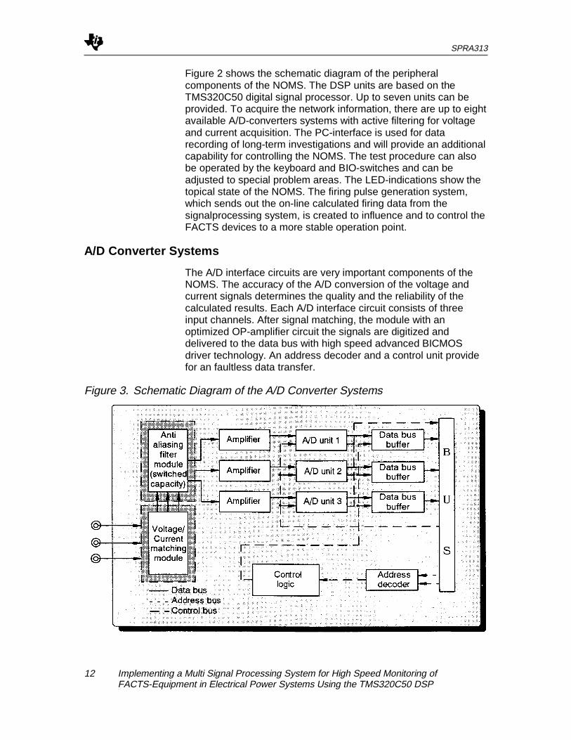
A/D Converter Systems
The A/D interface circuits are very important components of theNOMS. The accuracy of the A/D conversion of the voltage andcurrent signals determines the quality and the reliability of thecalculated results. Each A/D interface circuit consists of threeinput channels. After signal matching, the module with anoptimized OP-amplifier circuit the signals are digitized anddelivered to the data bus with high speed advanced BICMOSdriver technology. An address decoder and a control unit providefor an faultless data transfer.
Figure 3. Schematic Diagram of the A/D Converter Systems

SPRA313
Implementing a Multi Signal Processing System for High Speed Monitoring of 13FACTS-Equipment in Electrical Power Systems Using the TMS320C50 DSP
The scanning raster of all installed channels of the NOMS issynchronized to get an accurate subtraction result of the phaseangle measurement in a power supply network. It is very importantfor a digital measurement in a power supply network to provide asample data control unit adjusting the topical sample rate of theNOMS to the variable frequency of the power supply network.With the proper combination of sample control signals, it ispossible to apply A/D circuits with a variable timing behavior.
The A/D converter system can be changed from a voltageacquisition system to a current acquisition system easily with areplacement of a plug and socket connected module circuit. Theanti-aliasing filter circuit is available as a plug and socketconnected module circuit. Later expansions or improvements ofthe NOMS can be comfortably integrated with additional plug andsocket connected module circuits.
The voltage acquisition module provides a floating measurementfor high voltage signals up to 2 kV with a simple differentialamplifier circuit. There is no need for an optical isolation amplifier.Therefore we have no problems with non-linearity and pink noise.The test inputs can be changed from symmetrical to non-symmetrical voltage conditions.
The current acquisition module is based on a series connectedsensing device in the network transmission line. The isolation andamplification of the current signal is managed by a low-noise andlinear OP-circuit. Thus we get accurate and original currentsignals on a very simple way. Both modules have an inputprotection circuit which prevents destruction of the interfacecircuits by dangerous voltage (above 2 kV) and current (above100 A) levels.
D/A Converter Systems
The D/A converter system is much simplified when using highintegrated four-in-one circuits. The D/A converter circuit containsan on-chip data latch. Thus, data bus transfer can be effected witha simple control unit very comfortable. The simple addressdecoder circuit (74F138) is enough for high-speed bus arbitration.A wait-state circuit provides a suitable timing between the D/Aconverter system and the signalprocessing system. Normally weare running our bus data transfer system with one wait-state. Foreach channel it also provided a reconstruction filter reducingsignal distortions and glitches.

SPRA313
14 Implementing a Multi Signal Processing System for High Speed Monitoring ofFACTS-Equipment in Electrical Power Systems Using the TMS320C50 DSP
One D/A converter system is able to send out eight output signalssynchronously. With the quadruple multiplexed D/A convertercircuits, we can maintain a relatively low bus loading. This is veryimportant for such a large input-output system. Besides thealternatively switchable wait-state circuit helps to avoid accidentaldata transfer errors when running the high-speed (up to 50 MHz)digital signal processors from Texas Instruments.
Figure 4. Schematic Diagram of the D/A Converter System
Keyboard/Display Interface
The keyboard as well as the display interface are connected to thesignalprocessing unit with latch circuits. In this way the very shortaccess time of the signalprocessing unit can be used and therelatively long access time of the keyboard/display circuit aredecoupled and independently. A control unit is managing the righttiming. The bus loading is reduced using advanced BICMOS busdrivers. Furthermore, the interface consists of an addressdecoder, the terminals for the display and keyboard, Flag-indication and BIO-switches.
The keyboard can be interfaced by polling or interrupt. We havechosen the interrupt mode because polling produces a high busload and, with the interrupt mode, we can enter keyboard dataasynchronously. In addition, the TMS320C50 signal processorprovides a software tool to handle the management of interruptsvery comfortable.
SPRA313
Implementing a Multi Signal Processing System for High Speed Monitoring of 15FACTS-Equipment in Electrical Power Systems Using the TMS320C50 DSP
There is also a circuit provided which makes the keyboardswitches chatter-proof. The interrupt signal of the keyboard is alsodelayed to prevent input data errors. Consequently there is adecoupling of asynchronous inputs and output from the high-speed signalprocessing unit. To realize the varied facilities of theNOMS, in spite of the complex structure of the software program,and to get a simple handling of them, we have created aconsistent on-line parameter input system. This user interfaceconsists of the keyboard and the display described above. Withthem you can carry out an on-line entering of configurations datafor measurement and analysis. It is possible to switch over to thefeatures as:
q Selective acquisition of voltage and current values in a three-phase system
q On-line calculation of the network conditions
q On-line influencing and output of new parameters for theFACTS control
q Analysis of network harmonics and distortion with state phasorblocking
q Measurement of the line power with complex phasors of themomentary power flow
q Synchronous subtraction of absolute value and phase angle ofcomplex voltage phasors at several nodes in the network
without interrupting the signalprocessing system. Thedocumentation of the D/A output channels is normally provided byoscilloscope screens.

SPRA313
16 Implementing a Multi Signal Processing System for High Speed Monitoring ofFACTS-Equipment in Electrical Power Systems Using the TMS320C50 DSP
Figure 5. Schematic Diagram of the Keyboard/Display Interface
Multi-Signal Processing Architecture
It was an aim of our application to realize a system of independentDSP units without reducing the single processor performancenoticeably. Thus we decided for a realization with up to sevenequal DSP-applications which work as independent bus mastersand are able to communicate via a common system bus. Forcommunications there’s a suitable interface, we called it MultiProcessor Interface (MPI), with global memory (up to 32 kWorddata RAM), a global 16 bit flag register and several uniquefunctional units that will be described later. Accesses to the globaldata memory are performed in burst mode. This means that theMPI has its own address counter which is loaded by writing to abase address. Each following access only transfers data to thememory by increasing the base address on each access. This isrealized by using different I/O-ports of the TMS320C50 which aredecoded in a GAL (20V8) of the MPI.
SPRA313
Implementing a Multi Signal Processing System for High Speed Monitoring of 17FACTS-Equipment in Electrical Power Systems Using the TMS320C50 DSP
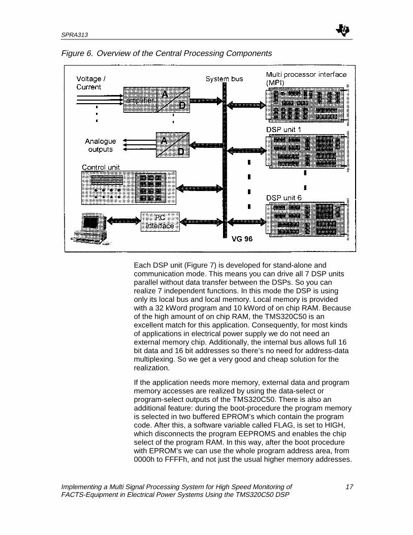
Figure 6. Overview of the Central Processing Components
Each DSP unit (Figure 7) is developed for stand-alone andcommunication mode. This means you can drive all 7 DSP unitsparallel without data transfer between the DSPs. So you canrealize 7 independent functions. In this mode the DSP is usingonly its local bus and local memory. Local memory is providedwith a 32 kWord program and 10 kWord of on chip RAM. Becauseof the high amount of on chip RAM, the TMS320C50 is anexcellent match for this application. Consequently, for most kindsof applications in electrical power supply we do not need anexternal memory chip. Additionally, the internal bus allows full 16bit data and 16 bit addresses so there’s no need for address-datamultiplexing. So we get a very good and cheap solution for therealization.
If the application needs more memory, external data and programmemory accesses are realized by using the data-select orprogram-select outputs of the TMS320C50. There is also anadditional feature: during the boot-procedure the program memoryis selected in two buffered EPROM’s which contain the programcode. After this, a software variable called FLAG, is set to HIGH,which disconnects the program EEPROMS and enables the chipselect of the program RAM. In this way, after the boot procedurewith EPROM’s we can use the whole program address area, from0000h to FFFFh, and not just the usual higher memory addresses.
SPRA313
18 Implementing a Multi Signal Processing System for High Speed Monitoring ofFACTS-Equipment in Electrical Power Systems Using the TMS320C50 DSP
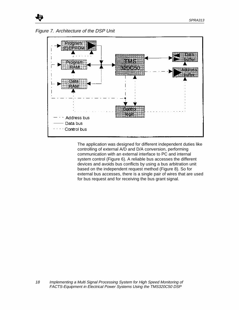
Figure 7. Architecture of the DSP Unit
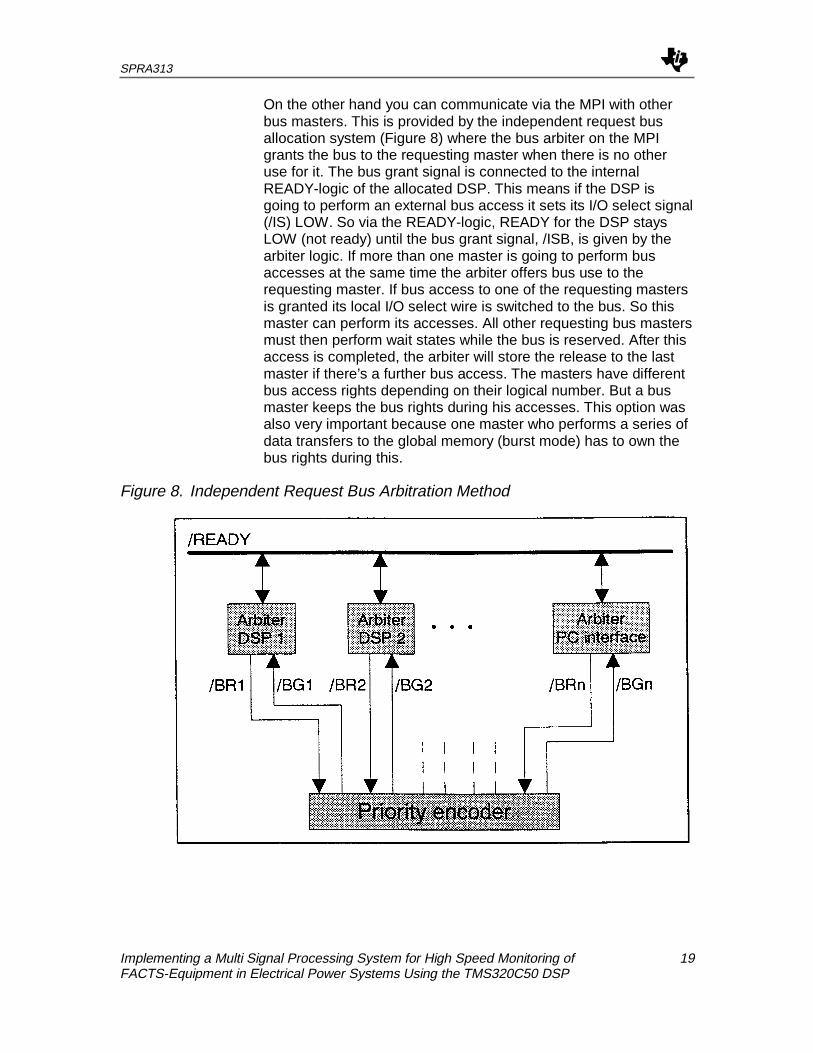
The application was designed for different independent duties likecontrolling of external A/D and D/A conversion, performingcommunication with an external interface to PC and internalsystem control (Figure 6). A reliable bus accesses the differentdevices and avoids bus conflicts by using a bus arbitration unitbased on the independent request method (Figure 8). So forexternal bus accesses, there is a single pair of wires that are usedfor bus request and for receiving the bus grant signal.
SPRA313
Implementing a Multi Signal Processing System for High Speed Monitoring of 19FACTS-Equipment in Electrical Power Systems Using the TMS320C50 DSP
On the other hand you can communicate via the MPI with otherbus masters. This is provided by the independent request busallocation system (Figure 8) where the bus arbiter on the MPIgrants the bus to the requesting master when there is no otheruse for it. The bus grant signal is connected to the internalREADY-logic of the allocated DSP. This means if the DSP isgoing to perform an external bus access it sets its I/O select signal(/IS) LOW. So via the READY-logic, READY for the DSP staysLOW (not ready) until the bus grant signal, /ISB, is given by thearbiter logic. If more than one master is going to perform busaccesses at the same time the arbiter offers bus use to therequesting master. If bus access to one of the requesting mastersis granted its local I/O select wire is switched to the bus. So thismaster can perform its accesses. All other requesting bus mastersmust then perform wait states while the bus is reserved. After thisaccess is completed, the arbiter will store the release to the lastmaster if there’s a further bus access. The masters have differentbus access rights depending on their logical number. But a busmaster keeps the bus rights during his accesses. This option wasalso very important because one master who performs a series ofdata transfers to the global memory (burst mode) has to own thebus rights during this.
Figure 8. Independent Request Bus Arbitration Method
SPRA313
20 Implementing a Multi Signal Processing System for High Speed Monitoring ofFACTS-Equipment in Electrical Power Systems Using the TMS320C50 DSP
Figure 9. Schematic Overview of the Multiprocessor Interface MPI
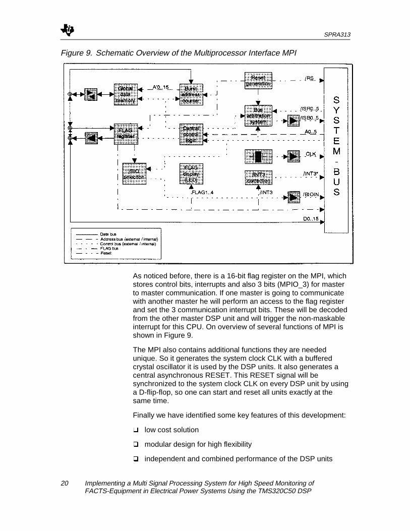
As noticed before, there is a 16-bit flag register on the MPI, whichstores control bits, interrupts and also 3 bits (MPIO_3) for masterto master communication. If one master is going to communicatewith another master he will perform an access to the flag registerand set the 3 communication interrupt bits. These will be decodedfrom the other master DSP unit and will trigger the non-maskableinterrupt for this CPU. On overview of several functions of MPI isshown in Figure 9.
The MPI also contains additional functions they are neededunique. So it generates the system clock CLK with a bufferedcrystal oscillator it is used by the DSP units. It also generates acentral asynchronous RESET. This RESET signal will besynchronized to the system clock CLK on every DSP unit by usinga D-flip-flop, so one can start and reset all units exactly at thesame time.
Finally we have identified some key features of this development:
q low cost solution
q modular design for high flexibility
q independent and combined performance of the DSP units
SPRA313
Implementing a Multi Signal Processing System for High Speed Monitoring of 21FACTS-Equipment in Electrical Power Systems Using the TMS320C50 DSP
q DSP performance of 28 MIPS
q fast global memory access in burst mode
q optional external program and data memory of 32 kWordavailable
Scalable Software Architecture
The following are the requirements of the software architecture:
q real-time processing and filtering of all input signals
q measurement for calculation of power, absolute values andphase difference in at least two nodes
q online selection of the complex space phasor of voltage,current or power
q flexible Fast Fourier Transformation for spectrum analysis
q simultaneous analysis of several input signals
q easy-to-use user interface
q modular structured software and expandable formultiprocessor operation
To accomplish these requirements this application uses theTMS320C50 from Texas Instruments. The hardware systemallows to measure four power nodes of voltage and current in twonetwork nodes. From this a great variety of network characteristiccan be calculated like the space phasor in each node as well incoordinates and in absolute value and phase. By combining thefour nodes (current and voltage) the momentary complex powerand the difference in absolute value and phase can be detected.The phase of the space phasor is also used to detect the netfrequency and to track the sample frequency. One special noveltyof this application is the real-time output of the rotated spacephasor. The rotation can be set to any given multiple of the netfrequency.
Another mode is used to calculate the Fast Fourier Transformationof the input signals or of the complex space phasor. The FFT canbe variable, calculated over a flexible number of samples with themaximum at 1024. A Hanning window can be added.
This application is implemented as several modules usingstructured programming techniques. Algorithms for transcendentalfunctions, filtering, controlling and I/O functions are recorded inlibraries.

SPRA313
22 Implementing a Multi Signal Processing System for High Speed Monitoring ofFACTS-Equipment in Electrical Power Systems Using the TMS320C50 DSP
Trigonometrical function are implemented using fast algorithmswith high resolution, e. g. the often called arc-tangent functionuses the fast cordic algorithm.
Figure 10. Software Architecture of the NOMS (2 of 4 Nodes)
SPRA313
Implementing a Multi Signal Processing System for High Speed Monitoring of 23FACTS-Equipment in Electrical Power Systems Using the TMS320C50 DSP
An oscillograph screen and a display make the measuring resultsvisual. A keyboard supports the flexibility of this system. Programmodes and variables can be changed online. Therefore lengthydownloads are not necessary. Controller parameters can be easilyoptimized and user defined output signals selected.
At this time, the software of the whole system, consisting of 12 AD(reading the test signals in the four nodes), 16 DAs (oscillographoutput), a keyboard (user defined online selection) and display(communication with the user and output signals), can beadministrated by two TMS320C50 DSP only.
The interrupt system is used to control peripheral elements in abackground process. The timer interrupt starts the input andoutput from and to the AD and DA converters in equal timedistances. This interrupt has the highest priority to avoid jittering ofthe sampled signals. Also, the display output uses this interrupt.Therefore an external buffering of display data is not necessary.Keyboard changes release an interrupt and are processed by amixture of polling and interrupt processing.
The high level of flexibility of this system is based on a userinterface that allows communication with the user and user-defined changes while processing. This possibility simplifies andaccelerates the development and is also proved as good for acomplex and variable real-time analyses of the supply networkcharacteristics.
SPRA313
24 Implementing a Multi Signal Processing System for High Speed Monitoring ofFACTS-Equipment in Electrical Power Systems Using the TMS320C50 DSP
Test Environment and Results
Transient Network Analyzer Test Installation
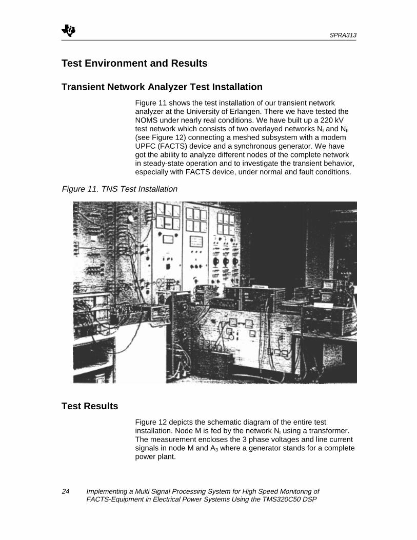
Figure 11 shows the test installation of our transient networkanalyzer at the University of Erlangen. There we have tested theNOMS under nearly real conditions. We have built up a 220 kVtest network which consists of two overlayed networks NI and NII
(see Figure 12) connecting a meshed subsystem with a modemUPFC (FACTS) device and a synchronous generator. We havegot the ability to analyze different nodes of the complete networkin steady-state operation and to investigate the transient behavior,especially with FACTS device, under normal and fault conditions.
Figure 11. TNS Test Installation
Test Results
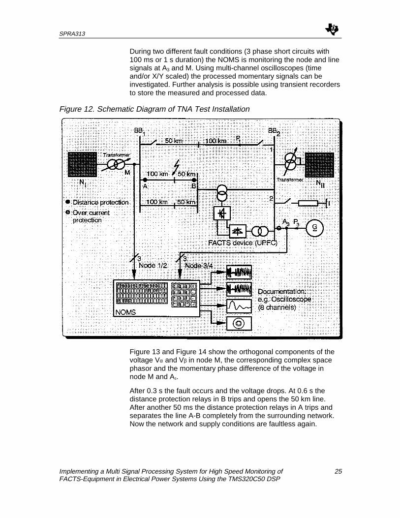
Figure 12 depicts the schematic diagram of the entire testinstallation. Node M is fed by the network NI using a transformer.The measurement encloses the 3 phase voltages and line currentsignals in node M and A3 where a generator stands for a completepower plant.
SPRA313
Implementing a Multi Signal Processing System for High Speed Monitoring of 25FACTS-Equipment in Electrical Power Systems Using the TMS320C50 DSP
During two different fault conditions (3 phase short circuits with100 ms or 1 s duration) the NOMS is monitoring the node and linesignals at A3 and M. Using multi-channel oscilloscopes (timeand/or X/Y scaled) the processed momentary signals can beinvestigated. Further analysis is possible using transient recordersto store the measured and processed data.
Figure 12. Schematic Diagram of TNA Test Installation
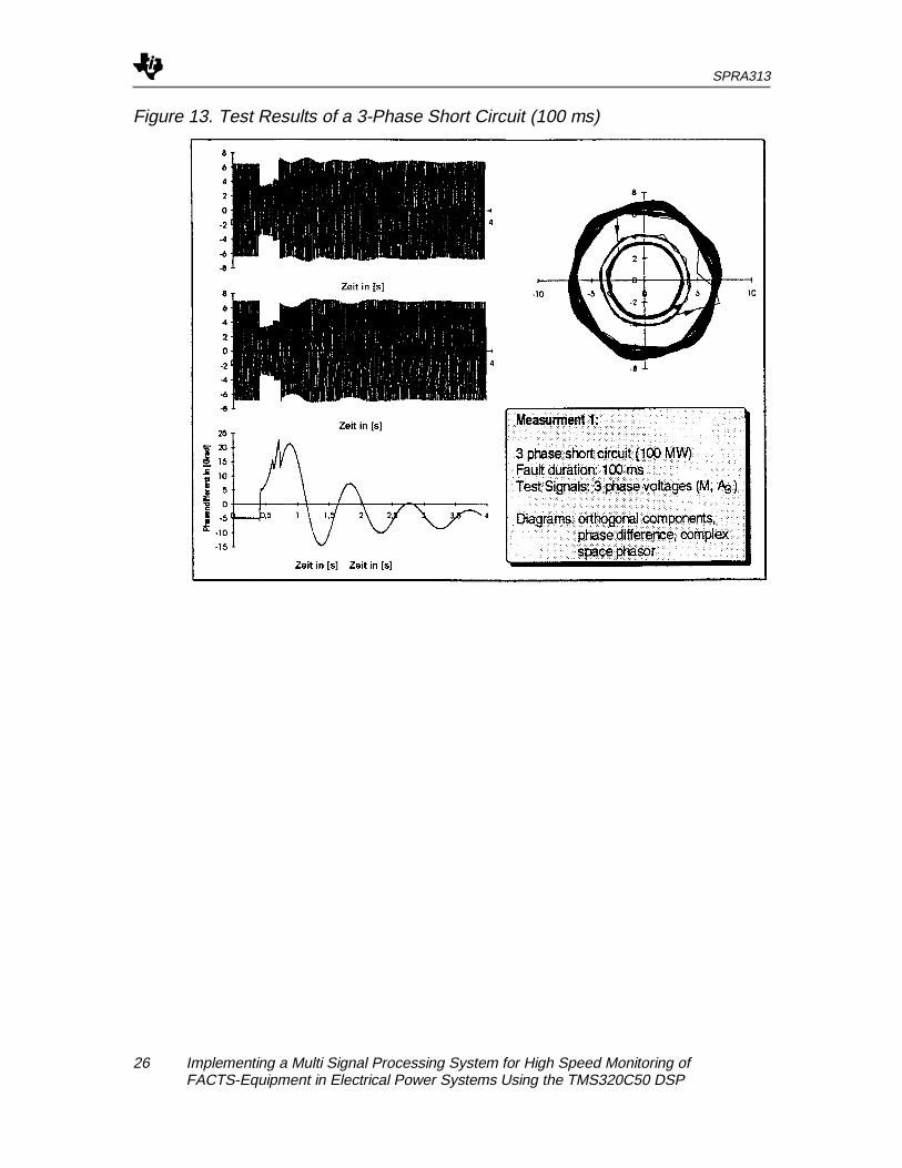
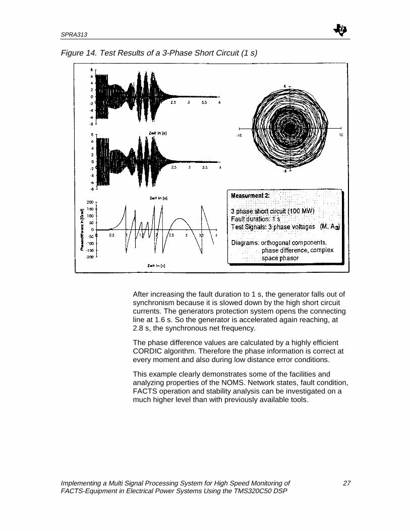
Figure 13 and Figure 14 show the orthogonal components of thevoltage Vα and Vβ in node M, the corresponding complex spacephasor and the momentary phase difference of the voltage innode M and A3.
After 0.3 s the fault occurs and the voltage drops. At 0.6 s thedistance protection relays in B trips and opens the 50 km line.After another 50 ms the distance protection relays in A trips andseparates the line A-B completely from the surrounding network.Now the network and supply conditions are faultless again.
SPRA313
26 Implementing a Multi Signal Processing System for High Speed Monitoring ofFACTS-Equipment in Electrical Power Systems Using the TMS320C50 DSP
Figure 13. Test Results of a 3-Phase Short Circuit (100 ms)
SPRA313
Implementing a Multi Signal Processing System for High Speed Monitoring of 27FACTS-Equipment in Electrical Power Systems Using the TMS320C50 DSP
Figure 14. Test Results of a 3-Phase Short Circuit (1 s)
After increasing the fault duration to 1 s, the generator falls out ofsynchronism because it is slowed down by the high short circuitcurrents. The generators protection system opens the connectingline at 1.6 s. So the generator is accelerated again reaching, at2.8 s, the synchronous net frequency.
The phase difference values are calculated by a highly efficientCORDIC algorithm. Therefore the phase information is correct atevery moment and also during low distance error conditions.
This example clearly demonstrates some of the facilities andanalyzing properties of the NOMS. Network states, fault condition,FACTS operation and stability analysis can be investigated on amuch higher level than with previously available tools.
SPRA313
28 Implementing a Multi Signal Processing System for High Speed Monitoring ofFACTS-Equipment in Electrical Power Systems Using the TMS320C50 DSP
Summary
Analyzing power supply networks is an interesting task for thefuture and necessary wherever different networks are interlinked.The development of digital signalprocessing systems make itpossible to measure different characteristic network parametersallowing a fast detection of network disturbances which can causedamage to electronic facilities. It can also be used to analyze andto control FACTS devices. The FACTS usage will increase in thenear future in the modern power supply systems.
Above we have presented an complete solution for a multi-signalprocessing system that is optimized for the application inelectrical power supply systems. The digital signal processorTMS320C50 of Texas Instruments is an excellent match for thisapplication because of its hardware and software architecture.
The new key features of our solution can be stated as follows:
q floating voltage measurement with a simple differential OPamplifier circuit (page 13)
q suitable sample rate control unit for power supply systems(page 13)
q low address and data bus loading (BICMOS technology, highlyintegrated D/A circuits, etc.) (page 13)
q decoupling of asynchronous inputs and outputs from the high-speed DSP units (page 14)
q consistent on-line parameter input system without aninterruption of the on-line data processing (page 15)
q each DSP unit represents a independent bus master in acommon bus system (page 16)
q multiprocessor interface (MPI) for high-speed communicationon a single bus system (page 16)
q optimized use of the on-chip memory of the TMS320C50(page 17)
q no need of internal address-data multiplexing (page 17)
q integration of a parallel addressed, transparent and high speedcache memory program space after the boot procedure withEEPROM (page 17)
q communication with other bus master units is provided by aglobal memory space (burst mode access), global registersand a bus allocation system for data consistency (page 19)
SPRA313
Implementing a Multi Signal Processing System for High Speed Monitoring of 29FACTS-Equipment in Electrical Power Systems Using the TMS320C50 DSP
q fast bus arbitration via the MPI unit using the independentrequest method (only two wires for each bus master required)(page 19)
q real-time FFT calculation and output of the complex rotatingspace phasors (page 21)
q all software is modular and stored in libraries (page 21)
q trigonometrical functions are implemented by optimizedCORDIC and/or linear interpolating table based algorithms(page 22)
q on-line user interface enables a flexible control over thesoftware flow (page 23)
q all external interrupts are managed by background processes(page 23)
q the software architecture realizes suitable access timings toslower peripheral components (e.g. display controllers) nobuffering or wait-states are required (page 23)
q highgrade of flexibility for on-line analysis and furtherdevelopments (page 23)
In the near future there will be a big demand for such systems inpower supply utilities. Therefore we will continue our successfuldevelopment with the Texasx Instruments digital signalprocessorcomponents.