in ga as nanowire growth on graphene: van der...
TRANSCRIPT

InxGa1−xAs Nanowire Growth on Graphene: van der Waals EpitaxyInduced Phase SegregationParsian K. Mohseni, Ashkan Behnam, Joshua D. Wood, Christopher D. English, Joseph W. Lyding,Eric Pop, and Xiuling Li*
Department of Electrical and Computer Engineering, Micro and Nanotechnology Laboratory, Beckman Institute for AdvancedScience and Technology, University of Illinois at Urbana−Champaign, Urbana, Illinois 61801, United States
*S Supporting Information
ABSTRACT: The growth of high-density arrays of verticallyoriented, single crystalline InAs NWs on graphene surfaces arerealized through the van der Waals (vdW) epitaxy mechanism bymetalorganic chemical vapor deposition (MOCVD). However, thegrowth of InGaAs NWs on graphene results in spontaneous phaseseparation starting from the beginning of growth, yielding a well-defined InAs−InxGa1−xAs (0.2 < x < 1) core−shell structure. Thecore−shell structure then terminates abruptly after about 2 μm inheight, and axial growth of uniform composition InxGa1−xAs takesplace without a change in the NW diameter. The InxGa1−xAs shellcomposition changes as a function of indium flow, but the coreand shell thicknesses and the onset of nonsegregated InxGa1−xAsaxial segment are independent of indium composition. In contrast,no InGaAs phase segregation has been observed when growing on MoS2, another two-dimensional (2D) layered material, or viathe Au-assisted vapor−liquid−solid (VLS) mechanism on graphene. This spontaneous phase segregation phenomenon iselucidated as a special case of van der Waals epitaxy on 2D sheets. Considering the near lattice matched registry between InAsand graphene, InGaAs is forced to self-organize into InAs core and InGaAs shell segments since the lack of dangling bonds ongraphene does not allow strain sharing through elastic deformation between InGaAs and graphene.
KEYWORDS: van der Waals epitaxy, nanowire, MOCVD, InGaAs, InAs, phase segregation, phase separation, graphene
Heteroepitaxy offers a route toward unification of thedistinct characteristics of dissimilar materials within a
monolithic structure that is otherwise not found in nature. Todate, one of the most exalted advantages offered bysemiconductor nanowires (NWs) is their ability to retaintheir crystalline quality under highly lattice-mismatchedheteroepitaxial growth conditions.1−4 The capacity for therelaxation of heterointerface-induced strain, offered by NWgeometries, prevents the formation of dislocations that plagueconventional highly mismatched bulk heterostructures.5−7
Based on this principle, already demonstrated NW-baseddevices such as lasers,8 light-emitting diodes,9 and photovoltaicsolar cells10,11 composed of compound semiconductors can beintegrated with more technologically mature platforms such asSi12−16 and more economically desirable substrate materials likeglass.17
Of particular interest for a novel class of optoelectronicdevices is the growth of semiconductor nanostructures onmechanically flexible and electrically conductive materials. Tothis end, Au-assisted growth of GaAs NWs on composite filmsof single-walled carbon-nanotubes18,19 and Si NWs on stainlesssteel foils20 have been demonstrated in recent years. In thesecases, the resultant NWs are oriented at a wide distribution ofangles with respect to the surface normal, due to a lack of long-
range atomic periodicity presented by the flexible substrates. Incontrast, graphene, having a two-dimensional (2D) planarconfiguration of sp2-bonded carbon atoms, possesses therequired combination of long-range atomic periodicity,mechanical strength and flexibility, high electrical conductivity,and optical transparency21−23 to serve as an ideal substrate forvertically aligned semiconductor NW growth for flexibleoptoelectronics.Recently, growths of various functional materials on
graphene layers have been reported, including thin films ofMoS2
24 and Cu-doped SnS,25 as well as GaAs,26 ZnO,27 andInAs28 one-dimensional (1D) nanostructures. Particularlyrelevant to the current work is the latter study carried out byHong et al.,28 wherein orientational control of InAs NWs,formed through van der Waals epitaxy (vdW Epi) by metal−organic chemical vapor deposition (MOCVD), was explored asa function of thickness and surface roughness of graphene-based substrates. vdW Epi refers to a particular crystal growthscenario wherein an epi-layer is formed on a substrate havingno dangling bonds.29 In such a scenario, the epi-layer/substrate
Received: December 10, 2012Revised: February 11, 2013Published: February 19, 2013
Letter
pubs.acs.org/NanoLett
© 2013 American Chemical Society 1153 dx.doi.org/10.1021/nl304569d | Nano Lett. 2013, 13, 1153−1161

interface is maintained purely through van der Waalsinteractions, allowing for dislocation-free incommensurategrowth.29
Although the material combination of InAs and graphenethrough vdW Epi has been previously reported, the nature ofepitaxial registry in such material systems and the growth ofternary compound semiconductor heterostructures on gra-phene remain unexplored. In this work, we present a self-organized method for the formation of coaxially heterostruc-tured InAs/InxGa1−xAs NWs, over a wide tunable ternarycompositional range, on large-area graphene substrates. Wedemonstrate that the self-organization phenomenon observed isunique to the InxGa1−xAs NW growth on graphene, asotherwise identical growths on Si substrates and MoS2 2Dsheets yield only stoichiometrically single phase InGaAs NWs.Moreover, we show that phase segregation does not occur forAu-assisted InGaAs NW growth on the same kind of graphenesubstrates. Therefore, we conclude that the preferential phasesegregation is the distinctive outcome of vdW Epi of a ternarycompound, in which a binary component is close to latticematched with the 2D substrate. Such heterogeneous nano-structures can be exploited for the fabrication of a novel class offunctional hybrid materials for use in flexible optoelectronicdevice applications.Growth of NWs was performed in an AIXTRON 200/4
MOCVD reactor through a seed-free, self-assembly mechanism.Trimethyl-indium [TMI, (CH3)3In], trimethyl-gallium [TMG,(CH3)3Ga], and arsine (AsH3) were used as the precursors forIn, Ga, and As, respectively. For this study, six NW samplegroups with different compositions, henceforth referred to asGroups 1−6, were investigated. The growth conditions used foreach sample group are summarized in Table 1, where ξ = χTMI/
(χTMI + χTMG), and χTMI and χTMG represent TMI and TMGmolar flow rates, respectively. Growth times were 10 min unlessotherwise indicated. Graphene growth was performed bychemical vapor deposition (CVD) on Cu (1 mil and 5 milthickness, 99.8% purity) with a process discussed previ-ously.30,31 Continuous sheets of monolayer graphene weretransferred to 90 nm SiO2/n++ Si by poly(methyl meth-acrylate) (PMMA).31,32 Discontinuous graphene samples werealso CVD-grown and transferred to SiO2 by a polybisphenol Acarbonate (PC) transfer method.33 Unless otherwise indicated,the graphene film is single layer; growth on multilayer graphenewas also examined, and no significant difference was found.Details of the NW growth and graphene preparation aredescribed in the Experimental Methods.First, we demonstrate the growth of high density InAs NW
arrays on graphene substrates. Figure 1a shows a dense array of
vertically oriented binary InAs NWs, with an average diameterof ∼87 nm (standard deviation of 17 nm) and average lengthsof ∼3.4 μm (standard deviation of 0.15 μm). The density ofthese NWs is estimated to be 7 × 108 cm−2, which is ∼7×higher as compared to that of previously reported InAs NWsgrown on graphene under comparable conditions.28 Weattribute the vertical alignment of NWs to the pseudocoherentrelationship between zincblende (Zb) InAs and the graphenesurface.28 This is because the lattice constant of Zb InAs alongthe ⟨110⟩ direction corresponds to the carbon−carbon bondlength of graphene (1.41 Å) by a multiple of 6.03. Thus, nearlylattice-matched growth of InAs crystals along the ⟨111⟩direction can be expected on (0001) graphene surfaces. Wehave found that such NW assembly depends strongly upongrowth temperature. Below 520 °C, NW formation is fullyquenched, and only parasitic island growth persists. On theother hand, growth temperatures above 580 °C result in thedecrease of NW density, likely due to a reduction of nucleationsites resulting from the enhanced desorption of growth species(Supporting Information, Figure S1). It should be noted thatnonvertical NW growth has been observed to occur on theparasitic islands and that island growth is predominant alongline defects present within graphene layers as well as at theedges of the graphene sheets (Supporting Information, FigureS2). A representative high-resolution transmission electronmicroscopy (HR-TEM) image obtained from the center of anInAs NW is shown in Figure 1b. As anticipated,28 the InAsNWs grown on graphene exhibit a Zb crystal structure withgrowth along the ⟨111⟩ direction. A high density of stackingfaults are observed, characterized as twin planes, similar to whathad been previously reported for seed-free, MOCVD-grown,InAs nanostructures.14,28 All InAs NWs show uniformdiameters throughout their lengths, with {−110} terminatedsidewall facets. Some NWs exhibit a slightly truncated sidewallprofile at the NW tip (∼4 nm long segment) (SupportingInformation, Figure S3).Of further interest is the degree of selectivity offered by
graphene films for NW growth. Figure 2 shows a tilted-viewSEM image of InAs NWs grown on a discontinuous graphenelayer, containing numerous regions of pristine graphene islands,among an otherwise graphene-free, SiO2 substrate. Thegraphene islands have dimensions on the order of tens ofmicrometers, separated by comparable lengths. The locations ofbare SiO2 and graphene-encapsulated SiO2 were confirmedprior to growth through AFM and Raman spectroscopycharacterization (Supporting Information, Figure S4). Theinset of Figure 2 shows the post-growth border (marked by adotted line) formed by a graphene island and the SiO2substrate. A clear areal selectivity is observed, insofar as NWformation is exclusively limited to the graphene-coveredregions. In contrast, polycrystalline island growth occurs onthe exposed oxide regions. Figure 2 demonstrates unambigu-ously that vdW Epi of vertical InAs NWs by MOCVD isselective to the graphene surface. Such selectivity can beexploited for the growth of patterned NW arrays by pregrowthlithographic patterning of graphene sheets. It should also benoted that the growth of such seed-free NWs places no adverseinfluence upon the structural quality of the graphene films, asdetermined through Raman scattering spectroscopy (Support-ing Information, Figure S5). We anticipate, therefore, thatdevice applications employing hybrid nanomaterials of thisnature may benefit from the dual role of graphene as both a
Table 1. Growth Conditions and Resultant InxGa1−xAs NWComposition for Various Sample Groups
NWgroup
growthtemperature
(°C)
growthduration(min)
gas phase In/(In+Ga)molar flow ratio, ξ
NW InxGa1−xAsPhase
composition, xa
1 550 10 1 12 570 10 0.65 0.743 570 10 0.59 0.564 570 10 0.52 0.395 570 10 0.42 0.296 570 10 0.27 0.21
aAs determined through XRD analysis.
Nano Letters Letter
dx.doi.org/10.1021/nl304569d | Nano Lett. 2013, 13, 1153−11611154

substrate for epitaxial growth and as an optically transparentelectrode.In addition to InAs NW growth on graphene substrates, we
have systematically studied ternary InxGa1−xAs NW growthover a wide composition range (0.2 < ξ < 1) on continuousgraphene films, as summarized in Table 1. To the best of ourknowledge, the current study represents the first demonstrationof growth of ternary InxGa1−xAs NWs on graphene substrates.The anticipated mismatch between InxGa1−xAs and graphene isonly ∼0.5% for x = 1 (InAs)26,28 and ∼5.65% for x ∼ 0.2.Figure 3a shows a representative SEM image of InxGa1−xAsNWs (Group 4 NWs, ξ = 0.52) grown over large areas undersimilar growth condition as that of InAs NWs. The inset showsa high magnification image of the same sample. SEM images forall other compositions can be found in the Supporting
Information (Figure S6). In comparison to pure binary InAsNWs, the average diameters of the InxGa1−xAs NWs increasefrom 87 ± 17 nm to 132 ± 24 nm, independent of indiumcomposition. Although all InxGa1−xAs NWs investigated hereare vertically aligned with respect to the graphene surface,roughly 40% exhibit a curved morphology near the NW top.Curved morphologies had been previously observed in the caseof Au-assisted InxGa1−xAs NWs34,35 and for seed-freeInxGa1−xAs NWs grown on Si (111),14 where the nature ofbending had been attributed to strain induced by compositioninhomogeneity. The NW curvature observed here appears toincrease with increasing Ga%, implying that more strain ispresent in the NW as the composition deviates from InAs.X-ray diffraction (XRD) measurements were carried out for
NW composition characterization. Figure 3b shows the XRD
Figure 1. High density vertical InAs NW growth on graphene. (a) 45° tilted-view SEM image of as-grown InAs NWs (Group 1) on a large area (1 ×1 cm2), defect-free graphene substrate with average NW density of 7 × 108 cm−2. (b) HR-TEM image of an InAs NW, showing a high density ofstacking faults along the NW. The white arrow points toward the NW tip.
Figure 2. Selective-area vdW Epi of InAs NWs on graphene. 45° tilted-view SEM image of InAs NWs grown on a discontinuous graphene film. NWgrowth occurs exclusively on the graphene islands. The inset shows a higher magnification image of the graphene (top)/SiO2 (bottom) boundary,delineated by the white dotted line.
Nano Letters Letter
dx.doi.org/10.1021/nl304569d | Nano Lett. 2013, 13, 1153−11611155

rocking curves for all NW groups, with intensity plotted on alogarithmic scale and offset vertically for clarity. The rockingcurve associated with each NW group is labeled with the gasphase molar flow ratio of group-III precursors, ξ, employedduring growth. Vertical dashed lines located at 25.4° and 27.3°denote the peak positions associated with diffraction from InAs(111) and GaAs (111) planes, respectively.36
Two key aspects of the XRD results shown in Figure 3brequire further discussion. First, the presence of the InAs (111)peak, labeled as peak “A”, is observed for all NW groups. Fromthe presence of peak A, it is understood that all NW samplespossess a phase consistent with (111) oriented crystalline InAs.Second, with the exception of group A NWs (purely InAs), allother NW groups exhibit an additional peak, labeled as peak“B”, situated between the position of the signals expected fromInAs (111) and GaAs (111). Peak B is, therefore, representativeof diffraction from InGaAs (111) planes. The position of peakB increases monotonically toward the GaAs (111) position withdecreasing values of gas phase In/(In + Ga) molar flow ratio, ξ,
as represented by the orange dashed arrow. Neglecting thePoisson ratio and assuming complete relaxation of the NWlattice, the In-composition of all InxGa1−xAs samples can bederived from the position of peak B, as summarized in Table 1.The broadening of the InGaAs peaks could be attributed tocompositional nonuniformity among the large collection ofindividual NWs, as well as island structures.The XRD results indicate that all ternary InxGa1−xAs NWs
over the wide compositional range studied have two distinctphases; namely, an InAs phase and an InGaAs phase. Thecomposition of the InGaAs phase changes as a function of gasphase In/(In+Ga) molar flow ratio, ξ. Given that all NWsamples were individually grown under constant TMI to TMGratios in a single step, the presence of two distinct phases isunexpected. To gain further insight into the phase segregationmechanism, scanning transmission electron microscopy(STEM) analysis was carried out on individual NWs from allInxGa1−xAs sample groups.Through high-angle annular dark-field (HAADF) imaging,
whereby contrast variations reflect compositional differencesdue to a high degree of Z-contrast, two distinct phases areidentified in individual InxGa1−xAs NWs. Figure 4a shows anHAADF image obtained from a region near the base of a NWfrom a Group 4 sample (ξ = 0.52). Here, two distinct segmentscan be observed: a central region of bright contrast,encapsulated by a peripheral region of relatively darker contrast.Therefore, a definitive core−shell heterostructure is found.Shown in Figure 4b is the energy dispersive X-ray (EDX)linescan results obtained across the NW as indicated by thedashed line in Figure 4a. Here, elemental counts of In, Ga, andAs are plotted as a function of radial position as black (square),red (circular), and blue (triangular) data points, respectively.Counts of elemental As increase toward the center region, incomparison to the peripheral regions, representative of theradial thickness profile of a cylindrical wire shape. At the centerof the NW, counts of elemental In increase while the elementalGa counts decrease, confirming the core−shell compositionchanges. Combining with the XRD data in Figure 3, theHAADF contrast variations and the radial EDX linescananalysis are consistent with a NW architecture wherein an InAscore is surrounded by an InGaAs shell. Note that the presenceof a finite Ga signal in the center is due to the presence ofelemental Ga in the shell segment.An HAADF image obtained from roughly the longitudinal
center of the same NW is shown in Figure 4c, wherein thewhite arrow points toward the NW tip. Here, two featuresshould be highlighted. First, closer to the base (left side) thesame radial heterostructure as shown in Figure 4a can bedistinguished. Second, moving toward the NW tip, a slightcontrast variation can be observed in the axial direction,corresponding to a transition to darker contrast closer to the tip(right side). Based on the axial EDX linescan shown in Figure4d and obtained along the dashed line in Figure 4c, thetransition toward the region of darker contrast closer to theNW tip corresponds to a point where a gradual decrease inelemental In and increase in elemental Ga simultaneouslyoccur. This transition represents a compositional variance fromInAs to InGaAs along the axial growth direction. Therefore, theformation of the InAs core becomes quenched while InGaAsaxial growth persists, resulting in a single phase InGaAs shellencapsulating the InAs core from all sides. The same structuralprofiles were observed for all other sample groups. It should benoted that the compositions of the InxGa1−xAs phases obtained
Figure 3. InxGa1−xAs NW growth on graphene. (a) Tilted view ofGroup 4 InxGa1‑xAs NWs (ξ = 0.52), with a higher magnificationimage shown in the inset. (b) Normalized XRD rocking curves plottedon a logarithmic scale, obtained from Group 1−6 NWs (from bottomto top). Each curve is labeled with the associated gas phase In/(In +Ga) molar flow ratio, ξ, as summarized in Table 1. Vertical dashedlines indicate the expected positions of InAs (111) and GaAs (111)diffraction signals. Peaks labeled A and B show the positions of theInAs and InGaAs peaks, respectively. The dashed orange line serves asa guide to the eye, tracing the evolution of the characteristic InGaAssignal with decreasing ξ.
Nano Letters Letter
dx.doi.org/10.1021/nl304569d | Nano Lett. 2013, 13, 1153−11611156

from XRD analysis, as specified in Table 1, are in agreementwithin <5% as compared to composition values obtainedthrough EDS point measurements.Although compositional inhomogeneity37 and phase segre-
gation38 in InGaAs nanowires have been recently reported, thecurrent study is the first example of a material system whereinan inert, 2D substrate directly influences the compositionalphase of the epi-layers. To more accurately access the evolutionof the observed segregation effect, the early stages of NWgrowth (2 and 5 min growth time) are examined (compared toa growth period of 10 min for all other NW groups discussedthus far). Figures S7a−c show tilted-view SEM images ofGroup 4 NWs after 2, 5, and 10 min growth periods,respectively. The mean NW length and diameter values as afunction of growth duration are quantified in Figure S7d of theSupporting Information. Two key features arise from thegrowth-evolution study. First, as the NW lengths increasenearly linearly with growth time, the NW diameters remainconstant within one standard deviation. Through HAADFanalysis (Supporting Information, Figure S8), it is determinedthat the average thickness of phase segregated InAs coresegments and InGaAs shell segments are fixed during the earlystages of growth. For all NWs analyzed, shell thickness valuesranging between 19 and 25 nm are measured, regardless of thetotal growth duration and composition. Therefore, wehypothesize that radial material segregation occurs in theearly stages of growth, possibly at time zero, and axialpropagation of growth fronts advance nearly in tandem forboth core and shell segments. How close to time zero will haveto be determined by higher time-resolution snap shots of theinitial growth and in situ TEM analysis. Second, for growth
times up to 5 min, NWs do not show curved or bentmorphologies. No evidence for single phase axial InGaAs NWgrowth is found by HAADF. This confirms that the curved NWmorphology is a direct result of strain induced bending in theaxial single phase InGaAs segment. Based on the NW axialgrowth rate, the onset of the single phase InGaAs NW growthoccurs right after 5 min. Beyond the 5 min growth period, axialextension of the InAs core segment is quenched, such that theInGaAs shell segment envelopes the core and extends the NWheight, as a single-stoichiometry InGaAs phase. Remarkably,there is no detectible change in diameter or composition andthe axial phase change onset position (∼2 μm from the NW/graphene interface) is independent of InGaAs composition.The mechanism of the axial growth termination of InAs coresegments is unclear at this point but should be related to thevan der Waals interaction of the InGaAs NW and graphenesubstrate, since the transition point appears to be independentof InGaAs composition. Future investigations, includinggrowths on h-BN sheets to evaluate the effect of the van derWaals attraction, growth interruption before the transition toevaluate surface preparation effects, as well as theoreticalmodeling of the energetics of the hybrid structure, will helpprovide more insight on the mechanism of this phenomenon.We believe that the radial heterostructure self-organization
process is a direct consequence of the commensuraterelationship of InAs lattice parameter with the nearest-neighborcarbon atom spacing of graphene.28 As strain sharing is notpermitted in the case of growth on an inert substrate, the binaryInAs component of ternary InGaAs preferentially self-assemblesas the core segment. To further evaluate this hypothesis, growthof InGaAs NWs on exfoliated MoS2 layers, deposited on SiO2
Figure 4. Phase-separated InGaAs NW. (a) HAADF image showing a region near the base of a Group 4 NW. The white dashed line shows theposition, x, along which the radial EDX linescan shown in (b) was obtained. (c) HAADF image from the central portion of the same NW as in (a).The black dashed line shows the position, x, where the axial EDX linescan shown in (d) was collected. The white arrows in (a) and (c) point towardthe NW tip; the scale bars represent a 25 nm length. Black (squares), red (circles), and blue (triangles) data points represent detected counts ofelemental In, Ga, and As, respectively.
Nano Letters Letter
dx.doi.org/10.1021/nl304569d | Nano Lett. 2013, 13, 1153−11611157

surfaces, has been performed. MoS2 was chosen as analternative growth surfaces based upon the following twocriteria: (1) as in the case of graphene, MoS2 is a planar (2D)material capable of accommodating vdW Epi growth;24 and (2)MoS2 has a lattice parameter of 3.16 Å (larger than graphene byapproximately 28%), offering an alternative surface atomicconfiguration with respect to graphene. As such, the role ofatomic registry in pseudo-lattice-matched InAs−graphene andlattice-mismatched InAs−MoS2 systems can be distinguished.InGaAs NW growth on exfoliated MoS2 flakes was carried outunder identical MOCVD growth conditions to that of theGroup 4 NW sample (ξ = 0.52) described above. Figure 5ashows a 45° tilted-view SEM image of InGaAs NWs on MoS2islands situated on a SiO2 background. To our knowledge, thisis the first demonstration of this particular materialcombination and exploration of this hybrid system. Althoughthe growth parameter space is not optimized yet, as can be seenin Figure 5a, vertical NW growth is achieved with heights up to5 μm and diameters in the 75−520 nm range. Despite therelatively high degree of parasitic island growth, NW bases can
be seen to stem directly from the surface of the MoS2substrates. The sparse nature of these NWs prevents theacquisition of meaningful XRD data from this sample. As such,compositional characterization was carried out exclusivelythrough STEM and EDX experiments. Figure 5b shows abright-field TEM image obtained from a single InGaAs NWsremoved from the MoS2 surface via ultrasonication. Additionaldiffraction pattern analysis (not shown) from the same NWdemonstrates a predominant Zb crystal structure with a highdensity of stacking faults, consistent with structural analysisperformed on Group 4 NWs. Figure 5c shows an HAADFimage obtained from the central segment of the same NW.Here, no spatially distinct compositional variances arediscerned, in contrast to all InxGa1−xAs NWs grown ongraphene substrates. The slight contrast increase toward thecenter of the NW shown in Figure 5c is attributed to theincreased thickness of the sample near its center. Furthermore,through EDX point analysis from various regions alongnumerous sets of InxGa1−xAs NWs grown on MoS2, it isestablished that these nanowires are homogeneous in
Figure 5. InGaAs NWs on MoS2 substrates. (a) 45° tilted-view SEM image of as-grown InGaAs NWs (ξ = 0.52) on an exfoliated MoS2 substrate.(b) Bright-field TEM image of an InGaAs NW removed from the MoS2 growth surface. The black arrow indicates the growth direction, as discernedfrom the slightly truncated tip structure. (c) HAADF-STEM images obtained from the midsection of the same NW shown in (b).
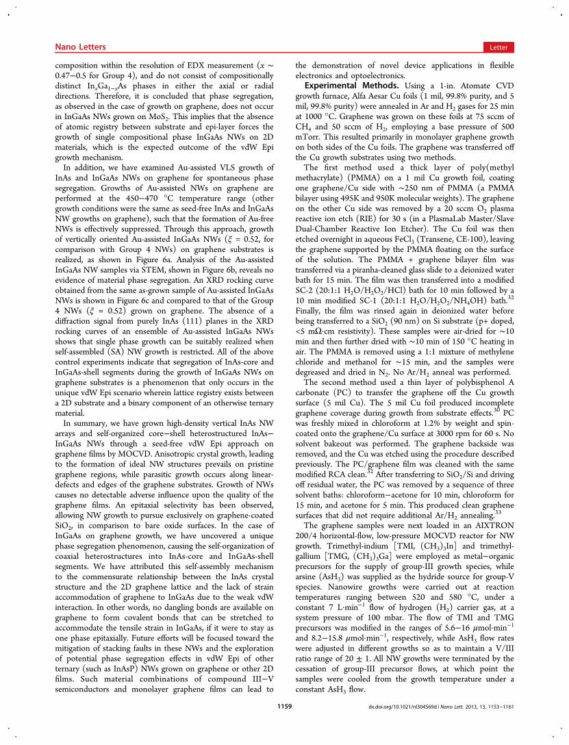
Figure 6. Au-assisted InGaAs NWs grown on graphene. (a) 45° tilted-view SEM image of as-grown Au-assisted InGaAs NWs on a graphenesubstrate. Au particles are visible at the NW tips, indicating VLS-type growth. (b) HAADF-STEM image obtained from the midsection of an Au-assisted InGaAs NW, showing no evidence of radial or axial phase segregation. (c) XRD rocking curves obtained from as-grown Au-assisted (Au-A,blue curve) and self-assembled (SA, black curve) InxGa1−xAs NW samples grown on graphene substrates (ξ = 0.52, for both cases).
Nano Letters Letter
dx.doi.org/10.1021/nl304569d | Nano Lett. 2013, 13, 1153−11611158
composition within the resolution of EDX measurement (x ∼0.47−0.5 for Group 4), and do not consist of compositionallydistinct InxGa1−xAs phases in either the axial or radialdirections. Therefore, it is concluded that phase segregation,as observed in the case of growth on graphene, does not occurin InGaAs NWs grown on MoS2. This implies that the absenceof atomic registry between substrate and epi-layer forces thegrowth of single compositional phase InGaAs NWs on 2Dmaterials, which is the expected outcome of the vdW Epigrowth mechanism.In addition, we have examined Au-assisted VLS growth of
InAs and InGaAs NWs on graphene for spontaneous phasesegregation. Growths of Au-assisted NWs on graphene areperformed at the 450−470 °C temperature range (othergrowth conditions were the same as seed-free InAs and InGaAsNW growths on graphene), such that the formation of Au-freeNWs is effectively suppressed. Through this approach, growthof vertically oriented Au-assisted InGaAs NWs (ξ = 0.52, forcomparison with Group 4 NWs) on graphene substrates isrealized, as shown in Figure 6a. Analysis of the Au-assistedInGaAs NW samples via STEM, shown in Figure 6b, reveals noevidence of material phase segregation. An XRD rocking curveobtained from the same as-grown sample of Au-assisted InGaAsNWs is shown in Figure 6c and compared to that of the Group4 NWs (ξ = 0.52) grown on graphene. The absence of adiffraction signal from purely InAs (111) planes in the XRDrocking curves of an ensemble of Au-assisted InGaAs NWsshows that single phase growth can be suitably realized whenself-assembled (SA) NW growth is restricted. All of the abovecontrol experiments indicate that segregation of InAs-core andInGaAs-shell segments during the growth of InGaAs NWs ongraphene substrates is a phenomenon that only occurs in theunique vdW Epi scenario wherein lattice registry exists betweena 2D substrate and a binary component of an otherwise ternarymaterial.In summary, we have grown high-density vertical InAs NW
arrays and self-organized core−shell heterostructured InAs−InGaAs NWs through a seed-free vdW Epi approach ongraphene films by MOCVD. Anisotropic crystal growth, leadingto the formation of ideal NW structures prevails on pristinegraphene regions, while parasitic growth occurs along linear-defects and edges of the graphene substrates. Growth of NWscauses no detectable adverse influence upon the quality of thegraphene films. An epitaxial selectivity has been observed,allowing NW growth to pursue exclusively on graphene-coatedSiO2, in comparison to bare oxide surfaces. In the case ofInGaAs on graphene growth, we have uncovered a uniquephase segregation phenomenon, causing the self-organization ofcoaxial heterostructures into InAs-core and InGaAs-shellsegments. We have attributed this self-assembly mechanismto the commensurate relationship between the InAs crystalstructure and the 2D graphene lattice and the lack of strainaccommodation of graphene to InGaAs due to the weak vdWinteraction. In other words, no dangling bonds are available ongraphene to form covalent bonds that can be stretched toaccommodate the tensile strain in InGaAs, if it were to stay asone phase epitaxially. Future efforts will be focused toward themitigation of stacking faults in these NWs and the explorationof potential phase segregation effects in vdW Epi of otherternary (such as InAsP) NWs grown on graphene or other 2Dfilms. Such material combinations of compound III−Vsemiconductors and monolayer graphene films can lead to
the demonstration of novel device applications in flexibleelectronics and optoelectronics.
Experimental Methods. Using a 1-in. Atomate CVDgrowth furnace, Alfa Aesar Cu foils (1 mil, 99.8% purity, and 5mil, 99.8% purity) were annealed in Ar and H2 gases for 25 minat 1000 °C. Graphene was grown on these foils at 75 sccm ofCH4 and 50 sccm of H2, employing a base pressure of 500mTorr. This resulted primarily in monolayer graphene growthon both sides of the Cu foils. The graphene was transferred offthe Cu growth substrates using two methods.The first method used a thick layer of poly(methyl
methacrylate) (PMMA) on a 1 mil Cu growth foil, coatingone graphene/Cu side with ∼250 nm of PMMA (a PMMAbilayer using 495K and 950K molecular weights). The grapheneon the other Cu side was removed by a 20 sccm O2 plasmareactive ion etch (RIE) for 30 s (in a PlasmaLab Master/SlaveDual-Chamber Reactive Ion Etcher). The Cu foil was thenetched overnight in aqueous FeCl3 (Transene, CE-100), leavingthe graphene supported by the PMMA floating on the surfaceof the solution. The PMMA + graphene bilayer film wastransferred via a piranha-cleaned glass slide to a deionized waterbath for 15 min. The film was then transferred into a modifiedSC-2 (20:1:1 H2O/H2O2/HCl) bath for 10 min followed by a10 min modified SC-1 (20:1:1 H2O/H2O2/NH4OH) bath.32
Finally, the film was rinsed again in deionized water beforebeing transferred to a SiO2 (90 nm) on Si substrate (p+ doped,<5 mΩ·cm resistivity). These samples were air-dried for ∼10min and then further dried with ∼10 min of 150 °C heating inair. The PMMA is removed using a 1:1 mixture of methylenechloride and methanol for ∼15 min, and the samples weredegreased and dried in N2. No Ar/H2 anneal was performed.The second method used a thin layer of polybisphenol A
carbonate (PC) to transfer the graphene off the Cu growthsurface (5 mil Cu). The 5 mil Cu foil produced incompletegraphene coverage during growth from substrate effects.30 PCwas freshly mixed in chloroform at 1.2% by weight and spin-coated onto the graphene/Cu surface at 3000 rpm for 60 s. Nosolvent bakeout was performed. The graphene backside wasremoved, and the Cu was etched using the procedure describedpreviously. The PC/graphene film was cleaned with the samemodified RCA clean.32 After transferring to SiO2/Si and drivingoff residual water, the PC was removed by a sequence of threesolvent baths: chloroform−acetone for 10 min, chloroform for15 min, and acetone for 5 min. This produced clean graphenesurfaces that did not require additional Ar/H2 annealing.
33
The graphene samples were next loaded in an AIXTRON200/4 horizontal-flow, low-pressure MOCVD reactor for NWgrowth. Trimethyl-indium [TMI, (CH3)3In] and trimethyl-gallium [TMG, (CH3)3Ga] were employed as metal−organicprecursors for the supply of group-III growth species, whilearsine (AsH3) was supplied as the hydride source for group-Vspecies. Nanowire growths were carried out at reactiontemperatures ranging between 520 and 580 °C, under aconstant 7 L·min−1 flow of hydrogen (H2) carrier gas, at asystem pressure of 100 mbar. The flow of TMI and TMGprecursors was modified in the ranges of 5.6−16 μmol·min−1
and 8.2−15.8 μmol·min−1, respectively, while AsH3 flow rateswere adjusted in different growths so as to maintain a V/IIIratio range of 20 ± 1. All NW growths were terminated by thecessation of group-III precursor flows, at which point thesamples were cooled from the growth temperature under aconstant AsH3 flow.
Nano Letters Letter
dx.doi.org/10.1021/nl304569d | Nano Lett. 2013, 13, 1153−11611159

Prior to NW growth, atomic force microscope (AFM)images were obtained using a Digital Instruments Dimension3000 setup in tapping mode, for the evaluation of graphenelayer location and thickness. The morphology, density, andorientation of the as-grown NW samples were inspected usingan Hitachi S-4800 field-emission scanning electron microscope(FE-SEM). X-ray diffraction (XRD) experiments wereperformed on as-grown NW samples using a PANanalytical/Philips X’Pert MRD system. Raman scattering spectroscopyanalysis of graphene samples was done, before and after NWgrowth, using a Renishaw inVia Raman microspectroscopysystem, with excitation provided by a 632 nm wavelength laserline and a spatial resolution of approximately 2.5 μm. Samplepreparation for analytical transmission electron microscopy(TEM) involved the ultrasonication of as-grown NW samplesin a small volume of methanol, followed by the dispersal of theresultant NW-containing solution on lacey-carbon-coated Cugrids. A JEOL 2010F scanning transmission electronmicroscopy (STEM) system was used for all TEM experiments.Site-specific compositional analysis of NW heterostructures wascarried out through high-angle annular dark-field (HAADF)imaging and energy dispersive X-ray (EDX) spectrometry usingthe JEOL 2010F microscope.
■ ASSOCIATED CONTENT
*S Supporting InformationGrowth temperature dependences, growth along parasiticislands, linear defects, and edges of graphene films, InAsnanowire tip structure, distinguishing graphene-coated vsexposed-oxide regions, influence of the nanowire growthprocess on graphene substrate quality, growth of InxGa1−xAsNWs on graphene, growth evolution of InGaAs on graphene,and STEM analysis of short growth period InGaAs NWs. Thismaterial is available free of charge via the Internet at http://pubs.acs.org.
■ AUTHOR INFORMATION
Corresponding Author*E-mail: [email protected].
NotesThe authors declare no competing financial interest.
■ ACKNOWLEDGMENTS
P.K.M. gratefully acknowledges Dr. Gregor Lawson forinsightful discussions. Financial support was provided in partby DOE under Award Numbers DEFG02-07ER46471 throughthe Frederick Seitz Materials Research Laboratory (P.K.M); theNational Science Foundation DMR under Award # 1006581(X.L.); the Air Force Office of Scientific Research (AFOSR)grant FA9550-10-1-0082 (E.P.), the Army Research Office(ARO) through the National Defense Science and EngineeringGraduate Fellowship (J.D.W.), the Beckman Foundation(J.D.W.), the National Science Foundation (NSF) grant CHE10-38015 (J.W.L.), and the Office of Naval Research (ONR)through grants N00014-10-1-0853 (A.B.). J.D.W. kindlyacknowledges assistance in sample preparation by G. P.Doidge. TEM work was carried out in the Frederick SeitzMaterials Research Laboratory Central Facilities, which arepartially supported by the U.S. Department of Energy undergrants DE-FG02-07ER46453 and DE-FG02-07ER46471.
■ REFERENCES(1) Martensson, T.; Svensson, C. P. T.; Wacaser, B. A.; Larsson, M.W.; Seifert, W.; Deppert, K.; Gustafsson, A.; Wallenberg, L. R.;Samuelson, L. Nano Lett. 2004, 4, 1987.(2) Bakkers, E. P. A. M.; van Dam, J. A.; De Franceschi, S.;Kouwenhoven, L. P.; Kaiser, M.; Verheijen, M.; Wondergem, H.; VanDer Sluis, P. Nat. Mater. 2004, 3, 769.(3) Ihn, S.-G.; Song, J.-I. Nano Lett. 2007, 7, 39.(4) Mohseni, P. K.; Maunders, C.; Botton, G. A.; LaPierre, R. R.Nanotechnology 2007, 18, 445304.(5) Zervos, M.; Feiner, L.-F. J. Appl. Phys. 2004, 95, 281.(6) Chuang, L. C.; Moewe, M.; Chase, C.; Kobayashi, N. P.; Chang-Hasnain, C. Appl. Phys. Lett. 2007, 90, 043115.(7) Ertekin, E.; Greaney, P. A.; Chrzan, D. C.; Sands, T. D. J. Appl.Phys. 2005, 97, 114325.(8) Hua, B.; Motohisa, J.; Kobayashi, Y.; Hara, S.; Fukui, T. NanoLett. 2009, 9, 112.(9) Qian, F.; Gradecak, S.; Li, Y.; Wen, C.-Y.; Lieber, C. M. NanoLett. 2005, 5, 2287.(10) Czaban, J. A..; Thompson, D. A.; LaPierre, R. R. Nano Lett.2009, 9, 148.(11) Colombo, C.; Heiβ, M.; Gratzel, M.; Fontcuberta i Morral, A.Appl. Phys. Lett. 2009, 94, 173108.(12) Svensson, C. P. T.; Martensson, T.; Tragardh, J.; Larsson, C.;Rask, M.; Hessman, D.; Samuelsson, L.; Ohlsson, J. Nanotechnology2008, 19, 305201.(13) Tomioka, K.; Motohisa, J.; Hara, S.; Hiruma, K.; Fukui, T. NanoLett. 2010, 10, 1639.(14) Shin, J. C.; Kim, K. H.; Yu, K. J.; Hu, H.; Yin, L.; Ning, C.-Z.;Rogers, J. A.; Zuo, J.-M.; Li, X. Nano Lett. 2011, 11, 4831.(15) Shin, J. C.; Mohseni, P. K.; Yu, K. J.; Tomasulo, S.;Montgomery, K. H.; Lee, M. L.; Rogers, J. A.; Li, X. ACS Nano2012, 6, 11074.(16) Shin, J. C.; Choi, K. J.; Kim, D. Y.; Choi, W. J.; Li, X. CrystalGrowth and Design 2012, 12, 2994.(17) Dhaka, V.; Haggren, T.; Jussila, H.; Jiang, H.; Kauppinen, E.;Huhtio, T.; Sopanen, M.; Lipsanen, H. Nano Lett. 2012, 12, 1912.(18) Mohseni, P. K.; Lawson, G.; Couteau, C.; Weihs, G.; Adronov,A.; LaPierre, R. R. Nano Lett. 2008, 8, 4075.(19) Mohseni, P. K.; Lawson, G.; Adronov, A.; LaPierre, R. R. IEEE J.Sel. Top. Quant. 2011, 17, 1070.(20) Tsakalakos, L.; Balch, J.; Fronheiser, J.; Korevaar, B. A.; Sulima,O.; Rand, J. Appl. Phys. Lett. 2007, 91, 233117.(21) Nonoselov, K. S.; Geim, A. K.; Morozov, S. V.; Jiang, D.; Zhang,Y.; Dubonos, S. V.; Grigorieva, I. V.; Firsov, A. A. Science 2004, 306,666.(22) Schwierz, F. Nat. Nanotechnol. 2010, 5, 487.(23) Bonoccorso, F.; Sun, Z.; Hasan, T.; Ferrari, A. C. Nat. Photonics2010, 4, 611.(24) Shi, Y.; Zhou, W.; Lu, A.-Y.; Fang, W.; Li, Y.-H.; Hsu, A. L.;Kim, S. M.; Kim, K. K.; Yang, H. Y.; Li, L.-J.; Idrobo, J.-C.; Kong, J.Nano Lett. 2012, 12, 2784.(25) Wang, W.; Leung, K. K.; Fong, W. K.; Wang, S. F.; Hui, Y. Y.;Lau, S. P.; Chen, Z.; Shi, L. J.; Cao, C. B.; Surya, C. J. Appl. Phys. 2012,111, 093520.(26) Munshi, A. M.; Dheeraj, D. L.; Fauske, V. T.; Kim, D.-C.; vanHelvoort, A. T. J.; Fimland, B.-O.; Weman, H. Nano Lett. 2012, 12,4570.(27) Kim, Y.-J.; Lee, J.-H.; Yi, G.-C. Appl. Phys. Lett. 2009, 95,213101.(28) Hong, Y. J.; Lee, W. H.; Wu, Y.; Ruoff, R.; Fukui, T. Nano Lett.2012, 12, 1431.(29) Koma, A. Thin Solid Films 1992, 216, 72.(30) Wood, J. D.; Schmucker, S. W.; Lyons, A. S.; Pop, E.; Lyding, J.W. Nano Lett. 2011, 11, 4547.(31) He, K. T.; Wood, J. D.; Doidge, G. P.; Pop, E.; Lyding, J. W.Nano Lett. 2012, 12, 2665.(32) Liang, X.; Sperling, B. A.; Calizo, I.; Cheng, G.; Hacker, C. A.;Zhang, Q.; Obeng, Y.; Yan, K.; Peng, H.; Li, Q.; Zhu, X.; Yuan, H.;
Nano Letters Letter
dx.doi.org/10.1021/nl304569d | Nano Lett. 2013, 13, 1153−11611160

Hight Walker, A. R.; Liu, Z.; Peng, L.-M.; Richter, C. A. ACS Nano2011, 5, 9144.(33) Lin, Y.-C.; Jin, C.; Lee, J.-C.; Jen, S.-F.; Suenaga, K.; Chiu, P.-W.ACS Nano 2011, 5, 2362.(34) Hou, J. J.; Han, N.; Wang, F.; Xiu, F.; Yip, S. P.; Hui, A. T.;Hung, T. F.; Ho, J. C. ACS Nano 2012, 6, 3624.(35) Jung, C. S.; Kim, H. S.; Jung, G. B.; Gong, K. J.; Cho, Y. J.; Jang,S. Y.; Kim, C. H.; Lee, C.-W.; Park, J. J. Phys. Chem. C 2011, 115, 7843.(36) Regolin, I.; Sudfeld, D.; Luttjohann, S.; Khorenko, V.; Prost, W.;Kastner, J.; Dumpich, G.; Meier, C.; Lorke, A.; Tegude, F.-J. J. Cryst.Growth 2007, 298, 607.(37) Hertenberger, S.; Funk, S.; Vizbaras, K.; Yadav, A.; Rudolph, D.;Becker, J.; Bolte, S.; Doblinger, M.; Bichler, M.; Scarpa, G.; Lugli, P.;Zardo, I.; Finley, J. J.; Amann, M.-C.; Abstreiter, G.; Koblmuller, G.Appl. Phys. Lett. 2012, 101, 043116.(38) Guo, Y.-N.; Xi, H.-Y.; Auchterlonie, G. J.; Burgess, T.; Joyce, H.J.; Gao, Q.; Tan, H. H.; Jagadish, C.; Shu, H.-B.; Chen, X.-S.; Lu, W.;Kim, Y.; Zou, J. Nano Lett. 2013, DOI: 10.1021/nl304237b.
Nano Letters Letter
dx.doi.org/10.1021/nl304569d | Nano Lett. 2013, 13, 1153−11611161