reduced graphene oxide/silicon nanowire heterostructures ... · pdf file1 table of contents...
TRANSCRIPT

Nano Res
1
Reduced graphene oxide/silicon nanowire
heterostructures with enhanced photoactivity and
superior photoelectrochemical stability
Xing Zhong1,†, Gongming Wang1,†, Benjamin Papandrea1, Mufan Li1, Yuxi Xu1, Yu Chen2, Chih-Yen Chen1,
Hailong Zhou1, Teng Xue2, Yongjia Li2, Dehui Li1 ,Yu Huang2,3 and Xiangfeng Duan1,3 ()
Nano Res., Just Accepted Manuscript • DOI 10.1007/s12274-015-0790-2
http://www.thenanoresearch.com on April 17, 2015
© Tsinghua University Press 2015
Just Accepted
This is a “Just Accepted” manuscript, which has been examined by the peer-review process and has been
accepted for publication. A “Just Accepted” manuscript is published online shortly after its acceptance,
which is prior to technical editing and formatting and author proofing. Tsinghua University Press (TUP)
provides “Just Accepted” as an optional and free service which allows authors to make their results available
to the research community as soon as possible after acceptance. After a manuscript has been technically
edited and formatted, it will be removed from the “Just Accepted” Web site and published as an ASAP
article. Please note that technical editing may introduce minor changes to the manuscript text and/or
graphics which may affect the content, and all legal disclaimers that apply to the journal pertain. In no event
shall TUP be held responsible for errors or consequences arising from the use of any information contained
in these “Just Accepted” manuscripts. To cite this manuscript please use its Digital Object Identifier (DOI®),
which is identical for all formats of publication.
Nano Research
DOI 10.1007/s12274-015-0790-2

1
TABLE OF CONTENTS (TOC)
Reduced Graphene Oxide-Silicon Nanowire
Heterostructures with Enhanced
Photoactivity and Superior
Photoelectrochemical Stability
Xing Zhong1,†, Gongming Wang1,†, Benjamin
Papandrea1, Mufan Li1, Yuxi Xu1, Yu Chen2,
Chih-Yen Chen1, Hailong Zhou1, Teng Xue2,
Yongjia Li2, Dehui Li1, Yu Huang2,3 and
Xiangfeng Duan1,3*
1 Department of Chemistry and Biochemistry,
University of California, Los Angeles, Los Angeles,
California, 90095, USA. 2 Department of Materials Science and Engineering,
University of California, Los Angeles, California,
90095, USA. 3 California Nanosystems Institute, University of
California, Los Angeles, California, 90095, USA.
† These authors contributed equally to this work.
Page Numbers.
We report a hybrid photocatalyst by enwrapping silicon nanowires with
reduced graphene oxide sheets to achieve greatly enhanced photoactivity and
superior photoelectrochemical stability.
Provide the authors’ website if possible.
Prof. Xiangfeng Duan, http://xduan.chem.ucla.edu/
2
Reduced Graphene Oxide/Silicon Nanowire Heterostructures
with Enhanced Photoactivity and Superior
Photoelectrochemical Stability
Xing Zhong1,†, Gongming Wang1,†, Benjamin Papandrea1, Mufan Li1, Yuxi Xu1, Yu Chen2, Chih-Yen Chen1, Hailong Zhou1, Teng Xue2, Yongjia Li2, Dehui Li1 ,Yu Huang2,3 and
Xiangfeng Duan1,3 ()
1 Department of Chemistry and Biochemistry, University of California, Los Angeles, Los Angeles, California, 90095, USA. 2 Department of Materials Science and Engineering, University of California, Los Angeles, California, 90095, USA. 3 California Nanosystems Institute, University of California, Los Angeles, California, 90095, USA.
† These authors contributed equally to this work.
Received: day month year / Revised: day month year / Accepted: day month year (automatically inserted by the publisher)
© Tsinghua University Press and Springer-Verlag Berlin Heidelberg 2011
ABSTRACT Silicon nanowires (SiNWs) have been widely explored as light harvesting antenna in photocatalysts due to
their ability to absorb broad solar spectrum, but are typically limited by poor photoelectrochemical stability.
Here we report the synthesis of reduced graphene oxide-SiNW (rGO-SiNW) heterostructures to achieve
greatly improved photocatalytic activity and stability. The SiNWs were synthesized through a metal-assisted
electroless etching process, and functionalized with reduced graphene oxide (rGO) flakes through a chemical
absorption process. Here the rGO can not only function as a physical protection layer to isolate the SiNWs
from the harsh electrochemical environment, but also serve as a charge mediator to facilitate the charge
separation and transport processes. Furthermore, the rGO may also function as the redox catalysts to ensure
efficient utilization of photo-carriers for the desired chemical reactions. Photocatalytic dye degradation
studies show that the photoactivity of the heterostructures can be significantly enhanced with an initial
activation process and maintained without apparent decay over repeated reaction cycles. Electrochemical
and photochemical studies indicate that the enhanced photoactivity and photostability can be attributed to
the more efficient separation of photoexcited charge carriers in SiNWs, and the reduced self-oxidation on
SiNWs surface during the photocatalytic dye degradation process. The ability to significantly improve the
photocatalytic activity and stability in rGO-SiNW heterostructures can not only open up more opportunities
in the application of silicon based photocatalysts/photoelectrodes for solar energy harvesting, but also
provide new insights in the stabilization of other unstable photocatalytic systems.
KEYWORDS Graphene, Silicon nanowire, Photocatalyst, Photoactivity, Stability
3
1. Introduction
Silicon based materials have garnered considerable
interest due to their unique properties and potential
applications in broad areas including electronics
[1-6], thermoelectrics [7], solar energy harvesting
[8-11], and biotechnology [12, 13]. With a room
temperature band gap of 1.12 eV, silicon promises
efficient solar energy harvesting across the entire
solar spectrum from UV to near infrared (IR) range.
To this end, silicon based photoelectrodes and
photocatalysts have been widely explored for solar
energy harvesting and conversion.
For photoelectrochemical or photocatalytic
processes, nanostructured materials typically
exhibit much better activity than their bulk
counterparts, due to their large surface areas and
short charge carrier diffusion distances [10, 14-17].
Therefore, nanoscale morphology engineering
represents one of the most common strategies to
develop highly efficient photocatalysts. We have
recently developed a metal-assisted electroless wet
chemical etching approach for the synthesis of
single crystal silicon nanowires (SiNWs) in large
quantity and explored their potential for efficient
photocatalysts [18-21]. With excellent optical
absorption, charge transport properties and large
surface area, these SiNWs have been shown to
exhibit excellent photocatalytic activity in the
visible range [18, 19, 22]. However, they are severely
limited by their poor photoelectrochemical stability
and rapid decay of the photoactivity under light
illumination. To this end, there have been
considerable efforts in developing effective
approaches to stabilize photoactivity of SiNWs,
typically using different surface protecting layers [4,
19, 23-26]. For example, Chen et al. have reported
the use of atomic layer deposition method to
deposit a thin TiO2 protection layer (~2 nm) on the
surface of SiNW photoelectrodes to enable excellent
photostability [24]. Qu et al. have designed an
integrated photocatalyst with a SiO2 protecting shell
to insulate SiNWs from direct photoelectrochemical
reactions and ensure excellent photoelectrochemical
stability [26]. These approaches, however, usually
involve complicated processes that are difficult to
scale up for large quantity production [18, 26].
Additionally, the use of an oxide-protecting layer
can usually result in a negative impact on both
charge separation and charge transport properties,
leading to a partially compromised photoactivity.
Therefore, there is a considerable interest in
developing alternative low cost and scalable
strategies for highly stable and active photocatalysts
based on SiNWs.
Graphene, a single atomic layer of honeycomb
lattice of carbon atoms, has recently become the
central focus of material research for both
fundamental studies and its potential applications
in diverse areas [27-34]. The covalently bonded
carbon lattice can exhibit excellent chemical stability
and function as a natural protecting barrier. For
example, it has been shown that graphene can
function as an effective passivation layer to protect
metal surfaces from oxidation [35, 36]. Additionally,
graphene can exhibit excellent electrical transport
properties and facilitate charge separation and
transport in semiconductors and their interfaces
[37-39]. Lastly, single or few layer graphene sheets
exhibit high optical transparency in visible
wavelengths [40], which will not affect the light
absorption of underlying materials. Together, these
combined attributes make graphene an excellent
candidate as a novel protection material and charge
mediating layer for SiNW photocatalysts.
Here, we report a facile and simple solution
phase method to enwrap SiNWs with reduced
graphene oxide (rGO) sheets. We show the
as-prepared rGO-SiNW heterostructures can exhibit
both enhanced photoactivity and remarkable
photostability. The improved photoactivity and
photostability is mainly attributed to the surface
protection of SiNWs by rGO and the more efficient
charge separation induced by the Schottky
junctions at the rGO-SiNW interface.

4
2. Experimental
2.1 Material preparation. The SiNWs in this study
were synthesized from a p-type silicon wafer (10-30
∙cm) through a wet chemical etching method.
Briefly, the silicon pieces were first sonicated in
acetone and isopropyl alcohol and then immersed
into a buffered oxide etchant (BOE) to remove the
native oxide layer. The H-terminated silicon pieces
were coated with Ag using an electroless deposition
process in a solution containing 0.005M AgNO3 and
4.8 M HF for 1 minute at room temperature. After Ag
deposition, the color of the silicon wafer surface turn
from dark to colorful. The resulting silver coated
silicon wafer was further rinsed with de-ionized
water to remove extra silver ions and then
immediately immersed into an etching solution
containing 4.8M HF and 0.3M H2O2 for 40 minutes.
Finally, the Ag nanoparticles were removed from the
nanowires by immersing in concentrated nitric acid
for one hour. The SiNWs were then scratched off the
substrate using a razor blade and collected for
further functionalization.
Graphene oxide sheets were prepared using an
improved Hummers’ method followed by strong
sonication [41]. The as-prepared graphene oxide
sheets were further reduced by a hydrazine solution
to produce the rGO solution for the subsequent
studies. To prepare the rGO-SiNW heterostructures,
1 mg of SiNW powder were dispersed in 3 ml of 2%
(3-Aminopropyl)triethoxysilane (APTES) ethanol
solution, stirred for 2 hrs and then centrifuged and
washed out with ethanol for three times. The APTES
functionalized SiNWs were re-dispersed in 5 ml of
water and mixed with various amount of rGO for 2
hrs under vigorous stirring. The product was finally
centrifuged and washed with water for three times.
2.2 Material characterization. The resulted rGO,
SiNWs and rGO-SiNWs were studied with a
scanning electron microscope (SEM) (JEOL 6700)
with 10 kV of electron acceleration voltage, or a
transmission electron microscope (TEM), high
resolution TEM (HRTEM), energy dispersive X-ray
spectroscopy (EDS) (Phillips CM120 with a 120 kV
operation voltage and FEI Titan with a 300 kV
operation voltage) and Raman spectroscopy with
488 nm laser wavelength (Renishaw 1000).
2.3 Photoactivity, electrochemical and
photoelectrochemical studies. Photocatalytic dye
degradation reactions were studied with SiNWs or
rGO-SiNWs in 100 mM of Indigo carmine (IC)
aqueous solution under a 300 W xenon lamp. The
rGO and SiNWs weight ratio in this experiment is
1:4. The IC degradation was monitored by a
Beckman DU-800 UV-vis spectrophotometer. All
photocatalytic reactions were carried out under
ambient conditions. Electrochemical and
photoelectrochemical studies were carried out using
a Princeton Applied Research electrochemical
workstation.
3. Results and discussion
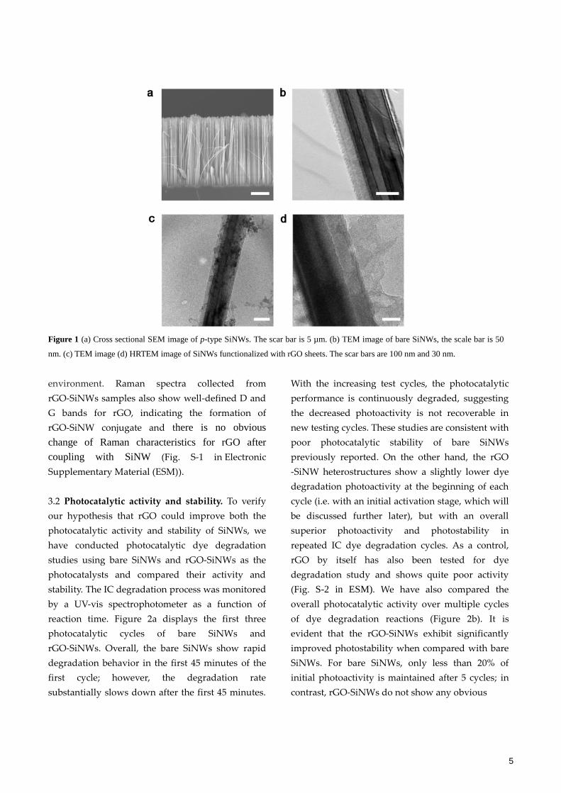
3.1 Structure of rGO-SiNWs. Figure 1a shows the
cross sectional SEM image of the etched SiNWs on a
p-type silicon wafer. It can be clearly seen that
SiNWs with a length of around 20 µm are produced
perpendicular to the substrate. The resulting SiNWs
can be removed from the substrate with a razor
blade and dispersed in proper solution for further
characterization, functionalization and
photocatalytic studies. Transmission electron
microscopy (TEM) studies show that the
as-prepared SiNWs typically exhibit diameters on
the order of 100 nm (Fig. 1b).
Before conjugating with rGO, the surface of
SiNWs was functionalized with APTES to render a
positive surface charge. The positively charged
SiNWs can then be coupled with negatively
charged rGO through the electrostatic interactions.
The TEM images of an rGO functionalized SiNW
clearly show that numerous pieces of rGO sheets
are closely wrapped on the surface of SiNWs (Fig.
1c, d), forming a physical diffusion barrier between
the silicon surface and the electrochemical
5
Figure 1 (a) Cross sectional SEM image of p-type SiNWs. The scar bar is 5 µm. (b) TEM image of bare SiNWs, the scale bar is 50
nm. (c) TEM image (d) HRTEM image of SiNWs functionalized with rGO sheets. The scar bars are 100 nm and 30 nm.
environment. Raman spectra collected from
rGO-SiNWs samples also show well-defined D and
G bands for rGO, indicating the formation of
rGO-SiNW conjugate and there is no obvious
change of Raman characteristics for rGO after
coupling with SiNW (Fig. S-1 in Electronic
Supplementary Material (ESM)).
3.2 Photocatalytic activity and stability. To verify
our hypothesis that rGO could improve both the
photocatalytic activity and stability of SiNWs, we
have conducted photocatalytic dye degradation
studies using bare SiNWs and rGO-SiNWs as the
photocatalysts and compared their activity and
stability. The IC degradation process was monitored
by a UV-vis spectrophotometer as a function of
reaction time. Figure 2a displays the first three
photocatalytic cycles of bare SiNWs and
rGO-SiNWs. Overall, the bare SiNWs show rapid
degradation behavior in the first 45 minutes of the
first cycle; however, the degradation rate
substantially slows down after the first 45 minutes.
With the increasing test cycles, the photocatalytic
performance is continuously degraded, suggesting
the decreased photoactivity is not recoverable in
new testing cycles. These studies are consistent with
poor photocatalytic stability of bare SiNWs
previously reported. On the other hand, the rGO
-SiNW heterostructures show a slightly lower dye
degradation photoactivity at the beginning of each
cycle (i.e. with an initial activation stage, which will
be discussed further later), but with an overall
superior photoactivity and photostability in
repeated IC dye degradation cycles. As a control,
rGO by itself has also been tested for dye
degradation study and shows quite poor activity
(Fig. S-2 in ESM). We have also compared the
overall photocatalytic activity over multiple cycles
of dye degradation reactions (Figure 2b). It is
evident that the rGO-SiNWs exhibit significantly
improved photostability when compared with bare
SiNWs. For bare SiNWs, only less than 20% of
initial photoactivity is maintained after 5 cycles; in
contrast, rGO-SiNWs do not show any obvious

6
Figure 2 (a) The comparison of the IC degradation catalyzed by the SiNWs (black square) and rGO-SiNWs (red dot) for the first
three cycles. (b) The photocatalytic stability of the SiNWs (black square) and rGO-SiNWs (red dot). The photoactivity of the both
photocatalysts is represented by the percentage of IC degraded at the reaction time of 105 minutes for each cycle.
Figure 3 (a). IC degradation catalyzed by functionalized rGO-SiNWs (red dot), physical mixture of rGO and SiNWs (blue square). (b)
Cyclic voltammogram curves of bare SiNWs (black), rGO (green), rGO-SiNWs (red) and physical mixture of rGO and SiNWs (blue)
in 0.5M Na2SO4 aqueous solution at a scan rate of 100 mV/s. (c) Continuous IC degradation catalyzed by the rGO-SiNWs.
Calculated amount of IC solution was added every 10 minutes after a total initial reaction time of 90 minutes.
decay in photocatalytic activity even after 10 cycles,
indicating rGO functionalization is an effective
method to stabilize the photoactivity of SiNWs.
To further understand the role of rGO in the
heterostructure photocatalysts, we have prepared a
physical mixture of rGO and SiNWs as a control
sample (Fig. S-3 in ESM) and investigated its
photocatalytic properties. Figure 3a shows that the
functionalized rGO-SiNWs and mechanically mixed
rGO/SiNWs (with the same SiNWs/rGO ratio)
exhibit very similar activation process and
photoactivity at the beginning; however, the IC dye
degradation rate of the mechanically mixed
rGO-SiNWs slows down shortly after the activation
process, which is different from the functionalized
rGO-SiNWs (without apparent decay). This decay
of photocatalytic activity in the physical mixture of
rGO and SiNWs may be attributed to the weak
interaction between rGO and SiNWs and the poor
protection of the SiNWs by the rGO.
It is noted that both mechanically mixed and
functionalized rGO-SiNWs show a similar
activation process, indicating that rGO is the key
factor responsible for the initial activation process.
Considering the large surface area of rGO, we
hypothesize the activation process is due to the
light driven internal charging effect [42]. Under
light irradiation, a large fraction of photogenerated
electron-hole pairs in SiNWs at the beginning are
used to charge rGO sheet, instead of the
photoelectrochemical process in solution. After the
initial charging process and when rGO is fully
charged, the photocatalytic activity shows an
apparent acceleration, as all the photogenerated

7
charges are used in the photocatalytic dye
degradation process from this point on. As a result,
the activation time in the photocatalytic process can
be understood by recognizing that the photoexcited
electron/hole pairs are not used for IC dye
degradation at the beginning but internal charging,
until the rGO based electrochemical capacitors are
fully charged.
To further understand the charging process, we
have conducted cyclic voltammogram (CV) of the
same amount of bare SiNWs, rGO, functionalized
rGO-SiNWs and physical mixture of rGO and
SiNWs in 0.5M Na2SO4 aqueous solution with a
scan rate of 100 mV/s (Fig. 3b). The significantly
increased rectangular CV area in the sample with
rGO indicates that the rGO-SiNWs has a more
pronounced charge storage capability compared to
bare SiNWs, resulting in a longer activation time. To
minimize the impact of the activation process on the
overall photocatalytic performance, we have further
performed the cycling experiment by repeatedly
adding a fixed amount of IC dye into the reaction
system at the end of each cycle, without
centrifuging out the photocatalysts. Significantly, no
activation stage is observed in the subsequent
reaction cycles since the electrochemical capacitor in
rGO-SiNW heterostructures has been already fully
charged during the first cycle (Fig. 3c). More
importantly, with the exclusion of the initial
charging process, the absolute photocatalytic
activity of rGO-SiNWs is at least one order of
magnitude higher than that of bare SiNWs (>90%
degradation in 10 minutes for rGO-SiNWs and
<70% degradation in 100 minutes for bare SiNWs).
The significantly enhanced photocatalytic
activity in rGO-SiNWs may be attributed to the
improved charge separation and transport at
rGO-SiNW interface, or the improved charge
injection efficiency from rGO to the solution (e.g.
the catalytic effect of rGO). To probe these
possibilities, we conducted systematic
electrochemical and photoelectrochemical studies.
Figure 4 (a) Cyclic voltammogram of bare SiNWs and rGO-SiNWs in 0.5 M Na2SO4 aqueous solution under N2 and O2 condition.
(b) Linear sweep of SiNWs and rGO-SiNWs in 0.5M Na2SO4 aqueous solution with IC dye under dark condition and light
illumination. (c) Photocurrent response of bare SiNWs (black curve) and rGO-SiNWs (red curve) at the potential of -1.5V vs.
Ag/AgCl under chopped light illumination. (d) Photocurrent response of bare SiNWs (black curve) and rGO-SiNWs (red curve) at a
fixed potential of 1V vs. Ag/AgCl under chopped light illumination.

8
As one of the photocatalytic reactions involves
oxygen reduction that generates reactive oxygen
species (ROS), we first studied the role of rGO for
oxygen reduction reaction. Figure 4a shows the
cyclic voltammogram of same amount of bare
SiNWs and rGO-SiNWs in 0.5M Na2SO4 solution
with/without oxygen. These plots clearly show that
rGO-SiNWs exhibit more pronounced oxygen
reduction activity than bare SiNWs, suggesting rGO
could facilitate oxygen reduction during the
photocatalytic process and thus improve the
photoactivity of the SiNWs.
By photoelectrochemical method, we have also
studied the separation of photoexcited charges at
the interface between rGO and SiNWs. Figure 4b
shows the linear sweep of bare SiNWs and
rGO-SiNWs in 0.5M Na2SO4 solution with IC dye at
the scan rate of 50 mV/s, under dark condition and
light illumination. As expected, both SiNWs and
rGO-SiNWs show cathodic photocurrents and the
rGO modification could enhance the photocurrent
density of SiNWs in the negative potential region.
Figure 4c shows the chopped cathodic
photocurrents of SiNWs and rGO-SiNWs at the
fixed potential of -1.5 V vs. Ag/AgCl. It also clearly
shows the photoresponse of rGO-SiNWs is much
higher than that of bare SiNWs, which is consistent
with the linear sweeps in Figure 4b. The increased
photocurrent is attributed to the more efficient
electron injection from silicon to rGO. A longer time
test with cathodic photocurrent of rGO-SiNWs
(Figure S-4 in ESM) further demonstrates the
photoelectrochemical stability of rGO-SiNWs. On
the other hand, in order to study the
hole-separation in rGO-SiNW interface, we applied
a reversible (positive) bias on silicon
photoelectrodes to tune the p-type property to
n-type behavior. As we can see in Figure 4d, both
bare SiNWs and rGO-SiNWs show anodic
photocurrent response with applying a positive
potential of 1.0 V vs. Ag/AgCl. Interestingly, the
rGO-SiNWs sample also shows higher photocurrent
density than that of bare SiNWs, suggesting rGO
can also facilitate the hole transport at the
rGO-SiNW interface.
Together, our studies have demonstrated
that rGO cannot only facilitate the electron injection,
but also hole injection process, which might be
attributed to the incomplete reduction and
heterogeneous nature of rGO (conjugated graphene
domains with oxygenic defects in between). These
different domains on rGO may form different types
of Schottky junctions with SiNWs to either facilitate
the electron or hole injection processes. For the
region with high degree of reduction, rGO would
be more like graphene and have a work function
around 4.5 eV [43], which can form a p-n junction
with p-type SiNWs with rGO facilitating the
electron separation and transport to solution. On
the other hand, it has been previously suggested the
less reduced region of rGO with oxygenic defects
could exhibit work function of 4.9 eV, more like
graphene oxide [44, 45], to align well with the
valence band of SiNWs. These parts of rGO could
facilitate the hole transport process. In this way, the
conjugation of rGO can not only function as an
effective protection layer to isolate the SiNW from
direction electrochemical process to ensure
excellent photostability, but also enhance the
electron hole separation and transport process to
greatly improve the photochemical activity.
Lastly, we have conducted TEM study on bare
SiNWs and rGO-SiNWs after photocatalytic testing.
Figure 5a,b show that a 5-10 nm amorphous SiOx
shell can be clearly seen on the SiNW surface after
photocatalytic testing. EDS studies (Fig. 5c) further
confirm that the apparent amorphous shell around
the SiNW consists of SiOx, suggesting the SiNW has
been severely oxidized during photocatalytic
process. In contrast, the SiNWs are well protected in
rGO-SiNW heterostructure by the enwrapping rGO
sheets. The rGO-SiNW interface remains clean

9
Figure 5 (a,b) TEM and selected area HRTEM images of the bare SiNW after photocatalytic reaction. The arrows indicate the
formation of silicon oxide shell. The scar bars are 100 nm and 5 nm, respectively. (c) Normalized energy dispersive X-ray spectra of
point A and B shown in (a), indicating the apparently amorphous shell primarily consists of SiOx. (d,e) TEM and selected area
HRTEM images of the SiNW functionalized with rGO after photocatalytic reactions. The arrows indicate the rGO on SiNW surface.
The scar bars are 100 nm and 5 nm respectively. (f) Normalized energy dispersive X-ray spectra of point A and B shown in (d),
indicating the primary presence of carbon outsize the crystalline silicon.
without obvious SiOx formation after the
photocatalytic process (Fig. 5d,e). The EDS studies
(Fig. 5f) further confirm that the amorphous layer
around the SiNW is not SiOx but the rGO
enwrapping the SiNW.
4. Conclusion
In summary, we have developed a simple and
effective strategy to protect SiNWs from oxidation
by functionalizing them with thin layer rGO sheets
and used them as highly efficient and stable
photocatalysts for dye degradation. Photocatalytic
studies demonstrate that the rGO enwrapped
SiNWs exhibit superior stability and photoactivity,
compared with the unprotected SiNWs.
Electrochemical and photoelectrochemical studies
suggest that the enhanced photoactivity and
photostability can be attributed to the physical
protection of SiNWs from direct photochemical
processes and the more efficient separation and
transport of photo-excited charges at rGO-SiNW
interface. The preparation of stable and efficient
rGO-SiNW photocatalysts could have enormous
impacts on the design and application of silicon
based materials for visible-light photocatalysis and
photoelectrochemical fuel generation.
Acknowledgements
We acknowledge the support from the U.S.
Department of Energy, Office of Basic Energy
Sciences, Division of Materials Science and
Engineering through Award DE-SC0008055. We
acknowledge Electron Imaging Center for
Nanomachines (EICN) at UCLA for the support of
TEM, supported with funding from NIH-NCRR
shared resources Grant (CJX1-443835-WS-29646)
and NSF Major Research Instrumentation Grant
(CHE-0722519).
Electronic Supplementary Material:
Supplementary material (Raman spectroscopy
10
measurement, TEM image of mechanical mixing
rGO/SiNWs, IC degradation catalyzed by rGO, and
long-time photocurrent stability test) is available in
the online version of this article at
http://dx.doi.org/10.1007/s12274-***-****-*
(automatically inserted by the publisher).
References
[1] Huang, Y.;Duan, X. F.;Cui, Y.;Lauhon, L. J.;Kim, K. H.; Lieber,
C. M. Logic gates and computation from assembled nanowire
building blocks. Science 2001, 294, 1313-1317.
[2] Cui, Y.; Lieber, C. M. Functional nanoscale electronic devices
assembled using silicon nanowire building blocks. Science 2001,
291, 851-853.
[3] Cui, Y.;Duan, X. F.;Hu, J. T.; Lieber, C. M. Doping and
electrical transport in silicon nanowires. J. Phys. Chem. B 2000,
104, 5213-5216.
[4] Qu, Y. Q.;Liao, L.;Li, Y. J.;Zhang, H.;Huang, Y.; Duan, X. F.
Electrically conductive and optically active porous silicon
Nanowires. Nano Lett. 2009, 9, 4539-4543.
[5] Huang, R. G.;Tham, D.;Wang, D. W.; Heath, J. R. High
performance ring oscillators from 10-nm wide silicon nanowire
field-effect transistors. Nano Res. 2011, 4, 1005-1012.
[6] Wang, D. W.;Sheriff, B. A.;McAlpine, M.; Heath, J. R.
Development of ultra-high density silicon nanowire arrays for
electronics applications. Nano Res. 2008, 1, 9-21.
[7] Tang, J. Y.;Wang, H. T.;Lee, D. H.;Fardy, M.;Huo, Z.
Y.;Russell, T. P.; Yang, P. D. Holey silicon as an efficient
thermoelectric material. Nano Lett. 2010, 10, 4279-4283.
[8] Jeong, S.;Garnett, E. C.;Wang, S.;Yu, Z. G.;Fan, S.
H.;Brongersma, M. L.;McGehee, M. D.; Cui, Y. Hybrid silicon
nanocone-polymer solar cells. Nano Lett. 2012, 12, 2971-2976.
[9] Garnett, E.; Yang, P. D. Light trapping in silicon nanowire solar
cells. Nano Lett. 2010, 10, 1082-1087.
[10] Qu, Y. Q.; Duan, X. F. Progress, challenge and perspective
of heterogeneous photocatalysts. Chem. Soc. Rev. 2013, 42,
2568-2580.
[11] Thiyagu, S.;Devi, B. P.; Pei, Z. W. Fabrication of large area
high density, ultra-low reflection silicon nanowire arrays for
efficient solar cell applications. Nano Res. 2011, 4, 1136-1143.
[12] Gunawardena, J. Silicon dreams of cells into symbols. Nat.
Biotechnol. 2012, 30, 838-840.
[13] Qing, Q.;Pal, S. K.;Tian, B. Z.;Duan, X. J.;Timko, B.
P.;Cohen-Karni, T.;Murthy, V. N.; Lieber, C. M. Nanowire
transistor arrays for mapping neural circuits in acute brain slices.
Proc. Natl. Acad. Sci. U. S. A. 2010, 107, 1882-1887.
[14] Wang, G. M.;Ling, Y. C.;Wang, H. Y.;Lu, X. H.; Li, Y.
Chemically modified nanostructures for photoelectrochemical
water splitting. J. Photochem. Photobiol. C-Photochem. Rev.
2014, 19, 35-51.
[15] Wang, G. M.;Ling, Y. C.; Li, Y. Oxygen-deficient metal oxide
nanostructures for photoelectrochemical water oxidation and
other applications. Nanoscale 2012, 4, 6682-6691.
[16] Zhou, H. L.;Qu, Y. Q.;Zeid, T.; Duan, X. F. Towards highly
efficient photocatalysts using semiconductor nanoarchitectures.
Energy Environ. Sci. 2012, 5, 6732-6743.
[17] Qu, Y. Q.;Zhong, X.;Li, Y. J.;Liao, L.;Huang, Y.; Duan, X. F.
Photocatalytic properties of porous silicon nanowires. J. Mater.
Chem. 2010, 20, 3590-3594.
[18] Qu, Y. Q.;Xue, T.;Zhong, X.;Lin, Y. C.;Liao, L.;Choi, J. N.;
Duan, X. F. Heterointegration of Pt/Si/Ag nanowire photodiodes
and their photocatalytic properties. Adv. Funct. Mater. 2010, 20,
3005-3011.
[19] Qu, Y. Q.;Cheng, R.;Su, Q.; Duan, X. F. Plasmonic
enhancements of photocatalytic activity of Pt/n-Si/Ag photodiodes
using Au/Ag core/shell nanorods. J. Am. Chem. Soc. 2011, 133,
16730-16733.
[20] Zhong, X.;Qu, Y. Q.;Lin, Y. C.;Liao, L.; Duan, X. F. Unveiling
the formation pathway of single crystalline porous silicon
nanowires. ACS Appl. Mater. Interfaces 2011, 3, 261-270.
[21] Qu, Y. Q.;Zhou, H. L.; Duan, X. F. Porous silicon nanowires.
Nanoscale 2011, 3, 4060-4068.
[22] Qu, Y. Q.; Duan, X. F. One-dimensional homogeneous and
heterogeneous nanowires for solar energy conversion. J. Mater.
Chem. 2012, 22, 16171-16181.
[23] Kenney, M. J.;Gong, M.;Li, Y. G.;Wu, J. Z.;Feng, J.;Lanza,
M.; Dai, H. J. High-performance silicon photoanodes passivated
with ultrathin nickel films for water oxidation. Science 2013, 342,
836-840.
[24] Chen, Y. W.;Prange, J. D.;Duhnen, S.;Park, Y.;Gunji,
M.;Chidsey, C. E. D.; McIntyre, P. C. Atomic layer-deposited

11
tunnel oxide stabilizes silicon photoanodes for water oxidation.
Nat. Mater. 2011, 10, 539-544.
[25] Hu, S.;Shaner, M. R.;Beardslee, J. A.;Lichterman,
M.;Brunschwig, B. S.; Lewis, N. S. Amorphous TiO2 coatings
stabilize Si, GaAs, and GaP photoanodes for efficient water
oxidation. Science 2014, 344, 1005-1009.
[26] Qu, Y. Q.;Liao, L.;Cheng, R.;Wang, Y.;Lin, Y. C.;Huang, Y.;
Duan, X. F. Rational design and synthesis of freestanding
photoelectric nanodevices as highly efficient photocatalysts.
Nano Lett. 2010, 10, 1941-1949.
[27] Wang, P.;Han, L.;Zhu, C. Z.;Zhai, Y. M.; Dong, S. J.
Aqueous-phase synthesis of Ag-TiO2-reduced graphene oxide
and Pt-TiO2-reduced graphene oxide hybrid nanostructures and
their catalytic properties. Nano Res. 2011, 4, 1153-1162.
[28] Bai, J. W.;Zhong, X.;Jiang, S.;Huang, Y.; Duan, X. F.
Graphene nanomesh. Nat. Nanotechnol. 2012, 5, 190-194.
[29] Bai, J. W.;Cheng, R.;Xiu, F. X.;Liao, L.;Wang, M. S.;Shailos,
A.;Wang, K. L.;Huang, Y.; Duan, X. F. Very large
magnetoresistance in graphene nanoribbons. Nat. Nanotechnol.
2010, 5, 655-659.
[30] Liao, L.;Lin, Y. C.;Bao, M. Q.;Cheng, R.;Bai, J. W.;Liu, Y.
A.;Qu, Y. Q.;Wang, K. L.;Huang, Y.; Duan, X. F. High-speed
graphene transistors with a self-aligned nanowire gate. Nature
2010, 467, 305-308.
[31] Liao, L.;Bai, J. W.;Cheng, R.;Lin, Y. C.;Jiang, S.;Huang, Y.;
Duan, X. F. Top-gated graphene nanoribbon transistors with
ultrathin high-k dielectrics. Nano Lett. 2010, 10, 1917-1921.
[32] Liu, Y.;Cheng, R.;Liao, L.;Zhou, H. L.;Bai, J. W.;Liu, G.;Liu, L.
X.;Huang, Y.; Duan, X. F. Plasmon resonance enhanced
multicolour photodetection by graphene. Nat. Commun. 2011, 2,
7.
[33] Wang, G. M.;Qian, F.;Saltikov, C.;Jiao, Y. Q.; Li, Y. Microbial
reduction of graphene oxide by Shewanella. Nano Res. 2011, 4,
563-570.
[34] Wang, B.;Liddell, K. L.;Wang, J. J.;Koger, B.;Keating, C. D.;
Zhu, J. Oxide-on-graphene field effect bio-ready sensors. Nano
Res. 2014, 7, 1263-1270.
[35] Li, X. Y.;Li, J.;Zhou, X. M.;Ma, Y. Y.;Zheng, Z. P.;Duan, X. F.;
Qu, Y. Q. Silver nanoparticles protected by monolayer graphene
as a stabilized substrate for surface enhanced Raman
spectroscopy. Carbon 2014, 66, 713-719.
[36] Chen, S. S.;Brown, L.;Levendorf, M.;Cai, W. W.;Ju, S.
Y.;Edgeworth, J.;Li, X. S.;Magnuson, C. W.;Velamakanni,
A.;Piner, R. D.;Kang, J. Y.;Park, J.; Ruoff, R. S. Oxidation
resistance of graphene-coated Cu and Cu/Ni alloy. ACS Nano
2011, 5, 1321-1327.
[37] Xiang, Q. J.; Yu, J. G. Graphene-based photocatalysts for
hydrogen generation. J. Phys. Chem. Lett. 2013, 4, 753-759.
[38] Xiang, Q. J.;Yu, J. G.; Jaroniec, M. Graphene-based
semiconductor photocatalysts. Chem. Soc. Rev. 2012, 41,
782-796.
[39] Wu, H. Y.;Xu, M.;Da, P. M.;Li, W. J.;Jia, D. S.; Zheng, G. F.
WO3-reduced graphene oxide composites with enhanced charge
transfer for photoelectrochemical conversion. Phys. Chem. Chem.
Phys. 2013, 15, 16138-16142.
[40] Bae, S.;Kim, H.;Lee, Y.;Xu, X. F.;Park, J. S.;Zheng,
Y.;Balakrishnan, J.;Lei, T.;Kim, H. R.;Song, Y. I.;Kim, Y. J.;Kim, K.
S.;Ozyilmaz, B.;Ahn, J. H.;Hong, B. H.; Iijima, S. Roll-to-roll
production of 30-inch graphene films for transparent electrodes.
Nat. Nanotechnol. 2010, 5, 574-578.
[41] Hummers, W. S.; Offeman, R. E. Preparation of graphitic
oxide. J. Am. Chem. Soc. 1958, 80, 1339-1339.
[42] Wang, G. M.;Ling, Y. C.;Lu, X. H.;Zhai, T.;Qian, F.;Tong, Y.
X.; Li, Y. A mechanistic study into the catalytic effect of Ni(OH)2
on hematite for photoelectrochemical water oxidation. Nanoscale
2013, 5, 4129-4133.
[43] Debgupta, J.;Mandal, S.;Kalita, H.;Aslam, M.;Patra, A.; Pillai,
V. Photophysical and photoconductivity properties of
thiol-functionalized graphene-CdSe QD composites. RSC Adv.
2014, 4, 13788-13795.
[44] Stratakis, E.;Sawa, K.;Konios, D.;Petridis, C.; Kymakis, E.
Improving the efficiency of organic photovoltaics by tuning the
work-function of graphene oxide hole transporting layers.
Nanoscale 2014, 6, 6925-6931.
[45] Yusoff, A. B.;Kim, H. P.; Jang, J. Inverted organic solar cells
with TiOx cathode and graphene oxide anode buffer layers. Sol.
Energy Mater. Sol. Cells 2013, 109, 63-69.

12
Electronic Supplementary Material
Reduced Graphene Oxide/Silicon Nanowire Heterostructures
with Enhanced Photoactivity and Superior
Photoelectrochemical Stability
Xing Zhong1,†, Gongming Wang1,†, Benjamin Papandrea1, Mufan Li1, Yuxi Xu1, Yu Chen2, Chih-Yen Chen1, Hailong Zhou1, Teng Xue2, Yongjia Li2, Dehui Li1 ,Yu Huang2,3 and
Xiangfeng Duan1,3 ()
1 Department of Chemistry and Biochemistry, University of California, Los Angeles, Los Angeles, California, 90095, USA. 2 Department of Materials Science and Engineering, University of California, Los Angeles, California, 90095, USA. 3 California Nanosystems Institute, University of California, Los Angeles, California, 90095, USA.
† These authors contributed equally to this work.
Received: day month year / Revised: day month year / Accepted: day month year (automatically inserted by the publisher)
© Tsinghua University Press and Springer-Verlag Berlin Heidelberg 2011
Figure S-1 Raman spectra of rGO and rGO-SiNWs. The broad peak located at around 970nm is originated from silicon, due to
2TO-photon overtone scattering from the critical point L. D and G bands are from graphene.
Figure S-2 IC degradation catalyzed by rGO itself.

13
Figure S-3 TEM image of mechanical mixture of rGO and SiNWs, showing poor adhesion between rGO and SiNWs. The scale bar is
500 nm.
Figure S-4 Photocurrent stability test of rGO-SiNWs at the potential of -1.5V vs. Ag/AgCl under chopped light illumination for 1
hour.