in-situ mems testing - nsti · 2015-03-01 · in-situ mems testing . a. schifferle*,**, a....
TRANSCRIPT

In-situ MEMS Testing
A. Schifferle
*,**, A. Dommann
*, A. Neels
* and E. Mazza
**,***
*CSEM,
Microsystems Technology Division, 2002 Neuchâtel, Switzerland, [email protected] **
Institut of Mechanical Systems, ETHZ, Tannenstrasse 3, 8092 Zurich, Switzerland ***
EMPA, Federal Institute of Materials Testing and Research, Ueberlandstr. 129, 8600 Duebendorf,
Switzerland
ABSTRACT
Related to the dramatically smaller volume of
microelectromecanical systems (MEMS), new methods in
testing and qualification are needed. On single crystal
silicon (SCSi) based devices, stress and loading in
operation introduces defects during the MEMS life time
and increases the risk of failure. Reliability studies on
potential failure sources have an impact on MEMS design
and are essential to assure the long term functioning of the
device.
In this paper, mechanical tests such as tensile
tests on SiSC beams are discussed to assess the resistance
of SCSi structures upon loading. Defects introduced by
DRIE, thermal annealing, dicing and bonding influence the
crystalline perfection and have a direct impact on the
mechanical properties of MEMS and on their aging
behavior. Strain, defects and deformations are analyzed
using High Resolution X-ray Diffraction Methods
(HRXRD). Supporting simulations are done by Finite
Element Method (FEM).
Keywords: reliability, microsystems, sensors, testing, x-ray
diffraction.
1 INTRODUCTION
Microelectromechanical systems engineering involves
complex design, manufacturing and packaging processes.
MEMS such as sensors, actuators, electronic devices find
applications in areas where a high reliability is needed, e.g.
aerospace, automotive or watch industry. In consequence
there is a strong demand in quality control and failure
analysis [1-5]. Microsystems technology (MST) can be
highly reliable, but differs from the reliability of solid-state
electronics. Therefore testing techniques must be developed
to accelerate MST-specific failures.
Single crystal materials, especially single crystal
silicon is preferentially used in MEMS technology as it
presents a high potential resistance against aging. The
crystal quality is influenced by the steps of the entire
engineering process. DRIE, thermal annealing, dicing and
bonding influence the crystalline perfection and could
favor failure.
For the understanding of failure it is essential to
obtain further going information about the stressed
material on the atomic scale. Therefore, detailed
investigations have to be conducted, which includes the
comparison of experimental methods as well as numerical
simulations. Experimental measurements of local strain,
deformations and the analysis of defects are approached by
High Resolution X-ray Diffraction Methods.
In-situ mechanical testing (Fig. 1 and 2) on the
HRXRD diffractometer is performed which allows to
evaluate the strain, defects and deformation during the
application of mechanical forces. The tensile tests are
executed on SiSC beams (50 x 50 m) fabricated by DRIE
etching and different post treatments (Fig. 3). HRXRD
(Fig. 2) with Rocking Curves (RC’s) and Reciprocal Space
Maps (RSM) is used as an accurate, non-destructive
experimental method to evaluate the SiSC quality in
MEMS, and more precisely for the given example, the in-
situ strain, defects and also geometrical parameters such as
tilt and bending of device parts. Simulations of
deformations by FEM are carried out simultaneously using
nonlinear constitutive laws based on well tested empirical
molecular potentials existing for SCSi [9-11].
2 EXPERIMENTAL
A new testing setup was developed to perform
mechanical testing on bending and on tensile specimen.
The flat design of the apparatus allows in-situ mechanical
testing on the HRXRD instrument which is performed and
gives the possibility to evaluate the strain, defects and
deformation during the application of mechanical forces
Fig 1: Experimental apparatus for tensile tests.
NSTI-Nanotech 2010, www.nsti.org, ISBN 978-1-4398-3402-2 Vol. 2, 2010 165
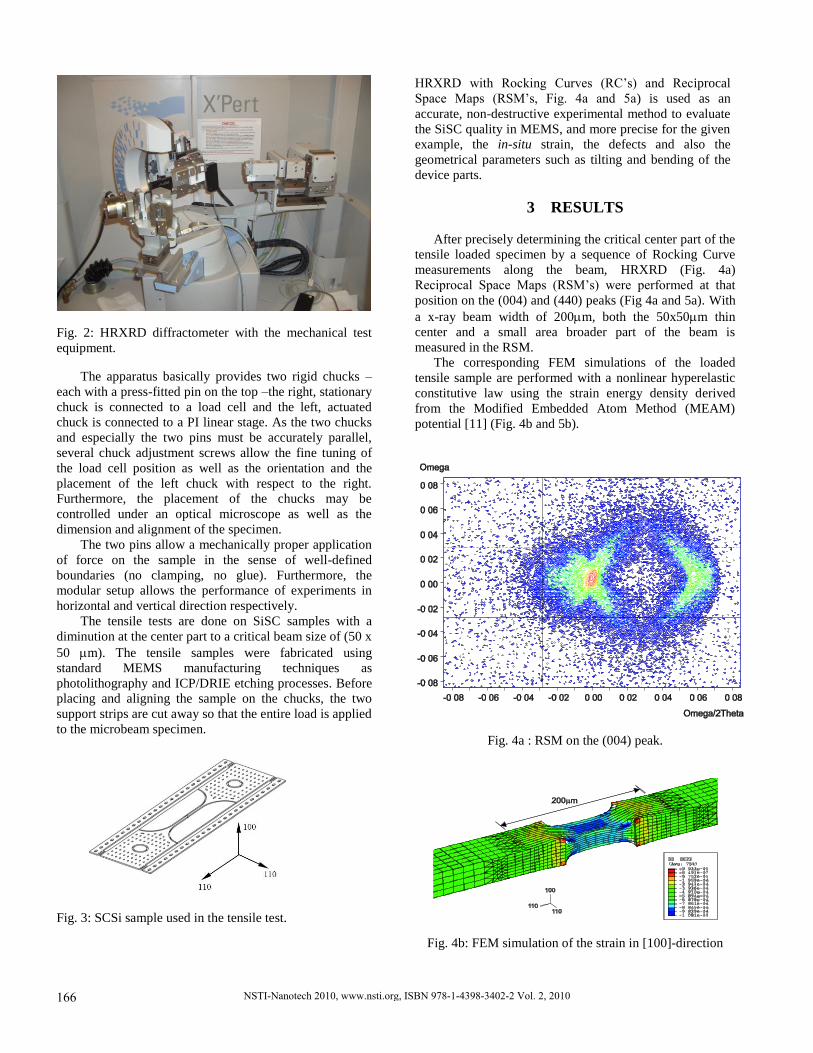
Fig. 2: HRXRD diffractometer with the mechanical test
equipment.
The apparatus basically provides two rigid chucks –
each with a press-fitted pin on the top –the right, stationary
chuck is connected to a load cell and the left, actuated
chuck is connected to a PI linear stage. As the two chucks
and especially the two pins must be accurately parallel,
several chuck adjustment screws allow the fine tuning of
the load cell position as well as the orientation and the
placement of the left chuck with respect to the right.
Furthermore, the placement of the chucks may be
controlled under an optical microscope as well as the
dimension and alignment of the specimen.
The two pins allow a mechanically proper application
of force on the sample in the sense of well-defined
boundaries (no clamping, no glue). Furthermore, the
modular setup allows the performance of experiments in
horizontal and vertical direction respectively.
The tensile tests are done on SiSC samples with a
diminution at the center part to a critical beam size of (50 x
50 m). The tensile samples were fabricated using
standard MEMS manufacturing techniques as
photolithography and ICP/DRIE etching processes. Before
placing and aligning the sample on the chucks, the two
support strips are cut away so that the entire load is applied
to the microbeam specimen.
Fig. 3: SCSi sample used in the tensile test.
HRXRD with Rocking Curves (RC’s) and Reciprocal
Space Maps (RSM’s, Fig. 4a and 5a) is used as an
accurate, non-destructive experimental method to evaluate
the SiSC quality in MEMS, and more precise for the given
example, the in-situ strain, the defects and also the
geometrical parameters such as tilting and bending of the
device parts.
3 RESULTS
After precisely determining the critical center part of the
tensile loaded specimen by a sequence of Rocking Curve
measurements along the beam, HRXRD (Fig. 4a)
Reciprocal Space Maps (RSM’s) were performed at that
position on the (004) and (440) peaks (Fig 4a and 5a). With
a x-ray beam width of 200m, both the 50x50m thin
center and a small area broader part of the beam is
measured in the RSM.
The corresponding FEM simulations of the loaded
tensile sample are performed with a nonlinear hyperelastic
constitutive law using the strain energy density derived
from the Modified Embedded Atom Method (MEAM)
potential [11] (Fig. 4b and 5b).
Fig. 4a : RSM on the (004) peak.
Fig. 4b: FEM simulation of the strain in [100]-direction
NSTI-Nanotech 2010, www.nsti.org, ISBN 978-1-4398-3402-2 Vol. 2, 2010166
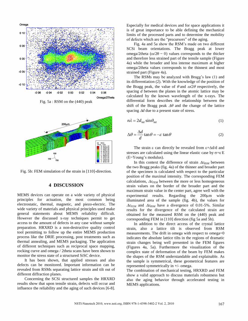
Fig. 5a : RSM on the (440) peak
Fig. 5b: FEM simulation of the strain in [110]-direction.
4 DISCUSSION
MEMS devices can operate on a wide variety of physical
principles for actuation, the most common being
electrostatic, thermal, magnetic, and piezo-electric. The
wide variety of materials and physical principles used make
general statements about MEMS reliability difficult.
However the discussed x-ray techniques permit to get
access to the amount of defects in any case without sample
preparation. HRXRD is a non-destructive quality control
tool permitting to follow up the entire MEMS production
process like the DRIE processing, post treatments such as
thermal annealing, and MEMS packaging. The application
of different techniques such as reciprocal space mapping,
rocking curve and omega / 2theta scans have been shown to
monitor the stress state of a structured SiSC device.
It has been shown, that applied stresses and also
defects can be monitored. Important information can be
revealed from RSMs separating lattice strain and tilt out of
different diffraction planes.
Concerning the SCSi structured samples the HRXRD
results show that upon tensile strain, defects will occur and
influence the reliability and the aging of such devices [6-8].
Especially for medical devices and for space applications it
is of great importance to be able defining the mechanical
limits of the processed parts and to determine the mobility
of defects which are the “precursors” of the aging.
Fig. 4a and 5a show the RSM’s made on two different
SCSi beam orientations. The Bragg peak at lower
omega/2theta (/2~ ) values corresponds to the thicker
and therefore less strained part of the tensile sample (Figure
4a) while the broader and less intense maximum at higher
omega/2theta values corresponds to the thinnest and most
strained part (Figure 4a).
The RSMs may be analyzed with Bragg’s law (1) and
its differentiation (2). With the knowledge of the position of
the Bragg peak, the value of and /2 respectively, the
spacing d between the planes in the atomic lattice may be
calculated by the known wavelength of the x-rays. The
differential form describes the relationship between the
shift of the Bragg peak and the change of the lattice
spacing d due to a present state of stress.
2 sinhkl hkln d (1)
tan tand
d
(2)
The strain can directly be revealed from =d/d and
stresses are calculated using the linear elastic case by =.E
(E=Young’s modulus).
In this context the difference of strain RSM between
the two Bragg peaks (fig. 4a) of the thinner and broader part
of the specimen is calculated with respect to the particular
position of the maximal intensity. The corresponding FEM
calculations, FEM between the more or less homogeneous
strain values on the border of the broader part and the
maximum strain value in the center part, agree well with the
experimental results. Regarding the 200m wide
illuminated area of the sample (fig. 4b), the values for
FEM and RSM have a divergence of 0.01-5%. Similar
results for the divergence of the calculated strain are
obtained for the measured RSM on the (440) peak and
corresponding FEM in [110] direction (fig 5a and 5b).
In addition to the direct access of the crystal lattice
strain, also a lattice tilt is observed from RSM
measurements. The drift in omega with respect to omega=0
indicates the absolute lattice tilts in the regions of dramatic
strain changes being well presented in the FEM figures
(Figures 4a, 5a). Furthermore the visualization of the
complex state of deformation of the beam by FEM makes
the shapes of the RSM understandable and explainable. As
the sample is symmetrical, these geometrical features are
represented symmetrically in +/- omega.
The combination of mechanical testing, HRXRD and FEM
show a valid approach to discuss materials robustness but
also the aging behavior through accelerated testing in
MEMS applications.
NSTI-Nanotech 2010, www.nsti.org, ISBN 978-1-4398-3402-2 Vol. 2, 2010 167
ACKNOWLEDGEMENTS
The here presented HRXRD investigations have been
applied to samples being provided by the Microsystems
Technology Division at CSEM.
REFERENCES
[1] A. Dommann, A. Neels, The role of strain in new
semiconductor devices, Advanced Engineering
Materials, 11, 275-277, 2009.
[2] A. Neels, A. Dommann, A. Schifferle, O. Papes, E.
Mazza, Reliability and Failure in Single Crystal
Silicon MEMS Devices, Microelectronics
Reliability, 48, 1245-1247, 2008.
[3] A. Neels, P. Niedermann, A. Dommann, Life time
predictions through X-ray defect analysis of
MEMS devices, Materials Science Forum, 584-
586, 518-522, 2008.
[4] E. Mazza, J. Dual, Mechanical behaviour of a mm-
sized single crystal silicon structure with sharp
notches, J. Mechanics and Physics of Solids 47
(1999), 1795-1821
[5] J.J. Wortmann and R.A. Evans, Young’s modulus,
shear modulus and Poisson’s ratio in silicon an
germanium, J. Appl. Phys., Vol. 44, 534-535,
1973
[6] Arney S.; Designing for MEMS Reliability, MRS
Bulletin, April 2001, p. 296
[7] Herbert R. Shea ; Reliability of MEMS for space
applications, Proc. SPIE Int. Soc. Opt. Eng. 6111,
61110A (2006)
[8] Dommann A., Enzler A., Onda N.; Advanced x-ray
analysis Techniques to Investigate Aging of
Micromachined Silicon Actuators for space
Application, Microelectronics Reliability, 43
(2003) 1099-1103
[9] F.H. Stillinger and T.A. Weber, Computer
simulation of local order in condensed phase of
silicon, Physical Riview B, 31(8):5262-5271, April
1985
[10] M.I. Baskes, Application of the Embedded-Atom
Method to Covalent Materials: A Semiempirical
Potential for Silicon, Physical Review Letters,
59(23):2666-2669, December 1987
[11] M.I. Baskes, Modified embedded-atom potentials
for cubic materials and impurities, Physical
Review B, 46(5):2727-2742, August 1942
NSTI-Nanotech 2010, www.nsti.org, ISBN 978-1-4398-3402-2 Vol. 2, 2010168