in this module you will learn: what the various logic gates do. how to represent logic gates on a...
TRANSCRIPT

In this module you will learn: What the various logic gates do.
How to represent logic gates on a circuit diagram.
The truth tables for the logic gates.
Boolean equations (the way we write logic expressions).
Logic gates
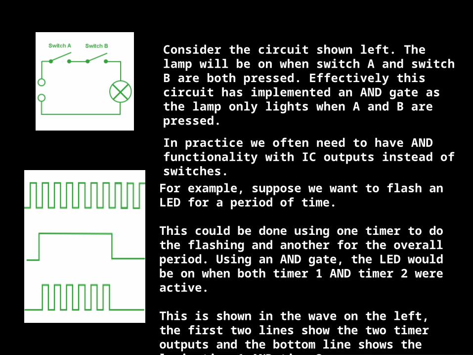
Consider the circuit shown left. The lamp will be on when switch A and switch B are both pressed. Effectively this circuit has implemented an AND gate as the lamp only lights when A and B are pressed.
In practice we often need to have AND functionality with IC outputs instead of switches.
For example, suppose we want to flash an LED for a period of time.
This could be done using one timer to do the flashing and another for the overall period. Using an AND gate, the LED would be on when both timer 1 AND timer 2 were active.
This is shown in the wave on the left, the first two lines show the two timer outputs and the bottom line shows the logic timer1 AND timer2.

As with all components, when we draw a circuit diagram, we need to use standard symbols so that other people can understand the circuit. The symbol shown on the left is an AND gate. The output Z is high when input A AND input B is high.
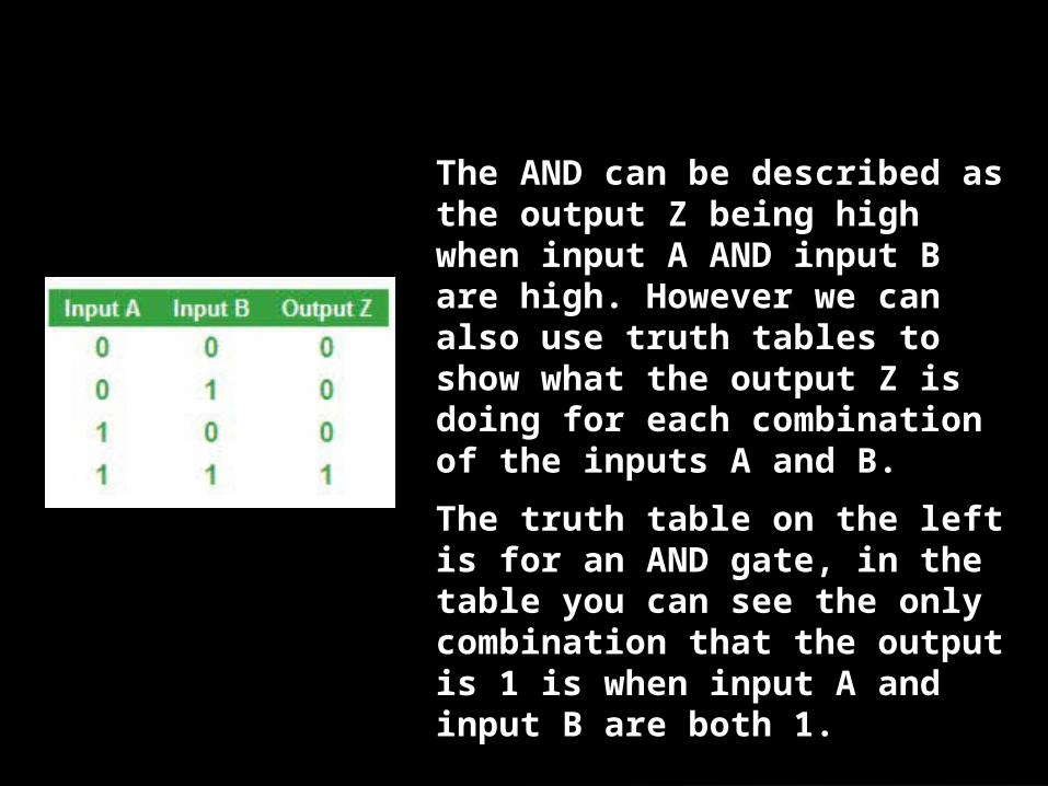
The AND can be described as the output Z being high when input A AND input B are high. However we can also use truth tables to show what the output Z is doing for each combination of the inputs A and B.
The truth table on the left is for an AND gate, in the table you can see the only combination that the output is 1 is when input A and input B are both 1.

The NOT gate or inverter only has one input. The output of the gate is always the opposite value to the input. The symbol and truth table for this gate are shown on the left.
With all logic a little circle on the end of the gate shows that it is a NOT. On the next page you will see that an AND gate with a circle makes a NOT AND gate.
NOT gate

The NAND gate is a NOT AND gate, which is shortened to NAND.
The output is on for all conditions, except when A and B are high. Hence it is the inverse of the AND gate.
NAND gate

The output of an OR gate is 1 if either input is 1.
OR gate

The NOR gate is a NOT OR.
So as with the NAND, we take the normal gate and NOT the output.
Hence with the NOR gate the output is 0 when either input is 1.
NOR gate

The XOR gate or exclusive OR, is similar to the OR gate however the output is a 1 when only 1 of the inputs is a 1.
XOR gate

Suppose we need to implement some logic where the output is on if the inputs (A and B) or C are on. We can use an AND gate as well as an OR gate and connect them together, as shown below:
For the circuit on the last page we could write Z = (A AND B) OR C
If we had a complicated expression that we wanted to write that used lots of gates then writing it out could take up lots of space and use lots of brackets and could get quite confusing.
Boolean algebra allows logic to be written in a simple way, where:
AND = . OR = + NOT = a line over the letter which is being inverted
Some examples are shown on the next page.

Examples

In summary