inas mos capacitors;fabrication &...
TRANSCRIPT

InAs MOS capacitors;Fabrication& CharacterizationFelix Vennberg
Bachelor Thesis 15 HP
Department of Physics
Supervisors: Aein S. Babadi & Lars-Erik Wernersson
Submitted: May 9, 2016
Examination: May 27, 2016

Abstract
The down scaling of metal-oxide-semiconductor based devices has been halted by the
shortcomings of silicon. To enable further miniaturization new materials are required.
The proposed replacements include compound III-V semiconductors and high-κ oxides,
the implementation of which has been difficult. This work investigates metal-oxide-
semiconductor capacitors fabricated on InAs substrate. The oxide layer was formed by
atomic layer deposition of high permittivity materials, ZrO2 and Al2O3. The quality of
the InAs-oxide interface was to be investigated after in situ surface treatment method in-
cluding cyclic nitrogen plasma and trimethylaluminum pulses. The measurements showed
a large dispersion in capacitance-voltage (C-V) data and a high leakage current through
the oxide layer. Possible sources of the defects leading to poor C-V behavior of the MOS
capacitors are subsequently investigated.

Contents
Abstract 1
Acronyms 2
1 Introduction 3
2 Theory 4
2.1 Metal- Oxide- Semiconductor . . . . . . . . . . . . . . . . . . . . . . . . . 4
2.2 Ideal Capacitance-Voltage . . . . . . . . . . . . . . . . . . . . . . . . . . . 5
2.3 Defects . . . . . . . . . . . . . . . . . . . . . . . . . . . . . . . . . . . . . . 7
2.4 Materials . . . . . . . . . . . . . . . . . . . . . . . . . . . . . . . . . . . . 9
3 Experiments 10
3.1 Fabrication of samples . . . . . . . . . . . . . . . . . . . . . . . . . . . . . 10
3.2 Measurements . . . . . . . . . . . . . . . . . . . . . . . . . . . . . . . . . . 12
4 Results & Discussion 13
4.1 Malfunctioning MOS capacitors . . . . . . . . . . . . . . . . . . . . . . . . 13
4.2 C-V data of Al2O3 samples . . . . . . . . . . . . . . . . . . . . . . . . . . . 16
5 Summary & Outlook 18
1

Acronyms
ALD Atomic Layer Deposition
C-V Capacitance-Voltage
I-V Current-Voltage
MOS Metal-Oxide-Semiconductor
MOSFET Metal-Oxide-Semiconductor Field-Effect-Transistor
TMA Trimethylaluminum
TEMAZ Tetrakis(ethylmethylamino)zirconium
2

1 Introduction
The invention of the metal-oxide-semiconductor (MOS) field-effect-transistor (FET) in
1960 by Khang and Atalla at Bell Laboratories enabled the creation of integrated circuits,
which are ubiquitous in today’s society [1, p. 3]. Since then the industry has striven to
miniaturize the technology in order to achieve higher computing power, reduce cost per
operation and allow for lower operating current [2]. Moore’s law famously predicted that
the number of devices on an integrated circuit doubles every 2-3 years and the size of each
component decreases exponentially [3].
The integral part of the many modern devices is a MOS. As the name suggests it
consists of a metal and a semiconductor separated by an oxide. Its function is to act
as a on/off switch, giving the device two states which can be used in logic operations.
The MOS based devices are advantageous compared to other devices because they are
exceptionally good at switching between states fast and efficiently. In addition, decreasing
their size improves on these characteristics [4].
The further down scaling has in recent years become complicated. silicon and its native
oxide has traditionally been used because of their outstanding performance, availability
and ease in manufacturing. However, the silicon oxide used as dielectric in a MOS is now
so thin that the leakage current due to direct tunneling is exceedingly high[3]. The high
leakage current results in higher power consumption, which is the greatest obstacle in the
field today [5].
Addressing this issue requires the introduction of new materials that have better prop-
erties such as III-V semiconductors with higher carrier mobility and oxides with higher
dielectric constant (κ). Promising oxides that have been tested include zirconium oxide
(ZrO2) and hafnium oxide (HfO2) [3]. Promising semiconductors include indium arsenide
(InAs) and indium gallium arsenide (InGaAs) [5].
The new materials brings another challenge in manufacturing. silicon dioxide is grown
directly on silicon and they have a good interface with each other. High-κ oxides have to
use more expensive deposition methods, form worse interfaces with other materials and
contain more overall defects [3]. The research today investigates procedures to overcome
these problems.
This work aims to investigate the properties of MOS capacitors with InAs semicon-
dunctor, ZrO2 oxide and nickel gate metal. Conditions and methods of manufacture are
varied to find one that overcomes the inherent flaws of the new materials.
3

2 Theory
2.1 Metal- Oxide- Semiconductor
The advantageous physical attributes of a MOS is derived from its composition. Figure
1 presents the basic MOS structure. As the name suggests it consists of a semiconductor
and a metal separated by a dielectric oxide.
Figure 1: MOS diode schematic, where V is applied voltage.
The composition generates a beneficial band structure. The band structure and how
it is affected when voltage is applied is a defining characteristic of a MOS diode. Figure
2 shows a MOS during flat-band condition, in this condition no charge is present at the
semiconductor-oxide interface.
EF
Ei
EV
EC
Energy
Metal Oxide Semiconductor
φM φS
Vacuum level
Figure 2: Band structure of ideal MOS at flat band condition
In Fig.2, EF is the Fermi level, EV the valence band of the semiconductor, Ei the
intrinsic Fermi level and EC represents the conduction band. The work functions φM and
φS are the differences between the Fermi level and the vacuum level on respective side.
When φM − φS = 0 the device is in flat band condition [1]. For an ideal MOS this occurs
when there is no voltage applied. Applying voltage to the metal plate results in three
general cases. The three cases are seen in Figure 3, where Ef is the Fermi level under
bias and EF the original Fermi level of the metal.
4

V > 0
Ef
EF
EV
Ei
EC
Electron
(a) Accumulation
V < 0
EF
Ef
EV
Ei
EC
(b) Depletion
V < 0
Ef
Ei
EV
EF
EC
Hole
(c) Inversion
Figure 3: Band bending of n-doped semiconductor
Figure 3a shows the accumulation phase of a MOS with a n-doped semiconductor. The
positive bias bends the bands near the semiconductor surface which causes electrons to
gather. The electron density is exponentially dependent on the energy difference EF −Ei.
As the intrinsic Fermi level dips more electrons accumulate, hence the name [1, p. 173].
When a small negative voltage is applied, as in Figure 3b, there are no charge carriers
at the surface. The electrons are pushed away by the negative potential and a depletion
region is formed. The depletion region grows with increased negative voltage until the
third phase, inversion, is reached. [1, p. 173].
Eventually the potential is negative enough to attract minority carriers in the semicon-
ductor to the surface, seen in Figure 3c. The density of holes is exponentially dependent
on Ei − EF and as the bands bend upwards the difference increases, leading to a higher
concentration. The n-doped semiconductor now has an area where the concentration of
holes exceed that of electrons, hence the name inversion. This area is called inversion
layer [1, p. 173].
Inversion is divided into two sub-categories, weak- and strong- inversion. To define
them let the difference between the intrinsic Fermi level and the original metal Fermi level
be Ei − EF = ED (see Figure 2). When no band bending is present let the ED = ED0 .
Weak inversion is then the period between ED = 0 and ED = −ED0 . Beyond that level
of band bending is the strong inversion [1, p. 175].
2.2 Ideal Capacitance-Voltage
The capacitance of a MOS depends on the voltage applied. In order to properly evaluate
the data obtained in the experiment it is vital to understand how this relation would be
expressed in a well behaved MOS. This is explained by how charges in the semiconductor
react to the bias.
The MOS structure is modeled as two capacitors in series, one over the oxide (Cox)
and the other over the depletion region (Cs). Cox is a fixed capacitor, whereas Cs is
variable and changes with the semiconductor charge. Cox is vital to the function of a
MOS, however how Cs behaves is of more interest.
5

Charges in the semiconductor induce an electrostatic potential. At the surface this
potential is called Ψs. Since the amount of charge at the surface (Qs) depends on the
bias, so does the surface potential. Cs can be described by the differential equation seen
in Eq. 1. Cs can thus be seen as a function of Ψs [1, p. 174].
Cs =dQs
dV(1)
Given that a MOS is two capacitors the voltage is split over the dielectric and the
semiconductor. This relation is described in Eq.2 where V0 is the potential over the oxide.
[1, p. 176].
V = V0 + Ψs (2)
The total capacitance (C) at a given voltage is then described by the usual series
relation in Eq. 3.
1
C=
1
Cox
+1
Cs(Ψs)(3)
With this the relation between voltage and capacitance can be understood. When
a MOS is in the accumulation phase there is an abundance of charges at the surface
so Cs(Ψs) is high, thus 1/Cs(Ψs) → 0 as Cs(Ψs) → ∞. The total capacitance (C)
is consequently equal to Cox. As the voltage sweeps towards zero a depletion region
forms. Charge carriers leave the surface and Cs(Ψs) decreases until it reaches a minimum.
Towards inversion minority carriers are gathered and Cs(Ψs) increases again. The effect
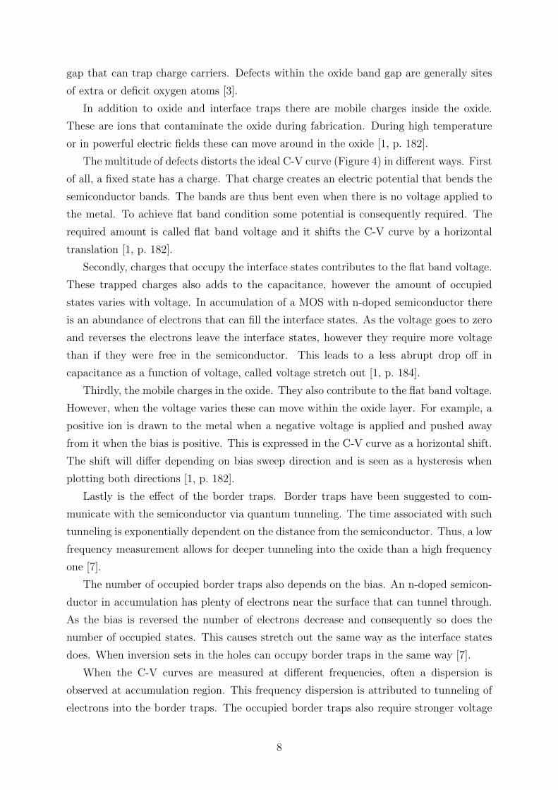
on C is seen in Figure 4.
Low f
High f
Accumulation
Depletion
InversionCox
Cmin
0
C[F ]
V[V]
Figure 4: C-V curve of an ideal MOS
In Figure 4 the curve splits after it reaches the minimum. As noted in the figure
this is due to the frequency (f) of the measurement. In a low frequency measurement
the generation-recombination of carriers in the depletion region is equal or faster than
6

the frequency. This leads to charge exchange with the inversion layer and the total
capacitance reaches Cox again. However in a high frequency measurement the minority
carrier response is not seen and thus the capacitance stays at the minimum [1, p. 178].
Figure 4 displays the capacitance-voltage (C-V) curve of an ideal MOS, however in
real measurements the C-V plot deviates from the ideal. This discrepancy stem from the
materials used. The cause and effect on the C-V curve is discussed in the remainder of
the Theory section.
2.3 Defects
Performance of a MOS is effected by the defects in the oxide and in the interface with the
semiconductor. There are two main types of defects, oxide- and interface-traps [6]. The
names refer to the location of the trap and is visualized in Figure 5.
××××××
Semiconductor
Interface trap
Oxide
-
-
-
- +
+
+
Oxide trap
Figure 5: Locations of oxide and interface traps
The defects are further categorized into whether or not they communicate electrically
with the semiconductor. Defects that exchanges charges with the semiconductor layer are
called switching states, those that do not are fixed states. Both oxide and interface traps
can be switching states [6].
Interface traps are defects that lie precisely at the oxide-semiconductor boundary,
they are mainly switching states. Border traps are near-interfacial oxide traps that elec-
trically functions as switching states on the time scale of the measurement. The ability to
electrically communicate decreases exponentially with the distance to the semiconductor.
The ability of the switching states to communicate with the semiconductor is depen-
dent on the bias condition and frequency of the measurement. Oxide traps have a higher
time constant associated with them than interface traps. Thus the higher the frequency
of measurement the fewer oxide traps will exchange charge with the semiconductor [6].
Defects caused by the presence of a foreign atom (impurities) or a structural defect
at semiconductor-oxide interface can create energy levels within the semiconductor band
7
gap that can trap charge carriers. Defects within the oxide band gap are generally sites
of extra or deficit oxygen atoms [3].
In addition to oxide and interface traps there are mobile charges inside the oxide.
These are ions that contaminate the oxide during fabrication. During high temperature
or in powerful electric fields these can move around in the oxide [1, p. 182].
The multitude of defects distorts the ideal C-V curve (Figure 4) in different ways. First
of all, a fixed state has a charge. That charge creates an electric potential that bends the
semiconductor bands. The bands are thus bent even when there is no voltage applied to
the metal. To achieve flat band condition some potential is consequently required. The
required amount is called flat band voltage and it shifts the C-V curve by a horizontal
translation [1, p. 182].
Secondly, charges that occupy the interface states contributes to the flat band voltage.
These trapped charges also adds to the capacitance, however the amount of occupied
states varies with voltage. In accumulation of a MOS with n-doped semiconductor there
is an abundance of electrons that can fill the interface states. As the voltage goes to zero
and reverses the electrons leave the interface states, however they require more voltage
than if they were free in the semiconductor. This leads to a less abrupt drop off in
capacitance as a function of voltage, called voltage stretch out [1, p. 184].
Thirdly, the mobile charges in the oxide. They also contribute to the flat band voltage.
However, when the voltage varies these can move within the oxide layer. For example, a
positive ion is drawn to the metal when a negative voltage is applied and pushed away
from it when the bias is positive. This is expressed in the C-V curve as a horizontal shift.
The shift will differ depending on bias sweep direction and is seen as a hysteresis when
plotting both directions [1, p. 182].
Lastly is the effect of the border traps. Border traps have been suggested to com-
municate with the semiconductor via quantum tunneling. The time associated with such
tunneling is exponentially dependent on the distance from the semiconductor. Thus, a low
frequency measurement allows for deeper tunneling into the oxide than a high frequency
one [7].
The number of occupied border traps also depends on the bias. An n-doped semicon-
ductor in accumulation has plenty of electrons near the surface that can tunnel through.
As the bias is reversed the number of electrons decrease and consequently so does the
number of occupied states. This causes stretch out the same way as the interface states
does. When inversion sets in the holes can occupy border traps in the same way [7].
When the C-V curves are measured at different frequencies, often a dispersion is
observed at accumulation region. This frequency dispersion is attributed to tunneling of
electrons into the border traps. The occupied border traps also require stronger voltage
8

than interface states to leave the oxide. The effect is a raised minimum capacitance and
a generally higher capacitance throughout the C-V curve.
To summarize, the switching-, fixed states and mobile carriers raises the flat band
voltage. The switching states creates a stretch out of the C-V curve and adds to the
capacitance. While the capacitance dispersion for different measurement frequencies in
accumulation region is usually attributed to the border trap response.
2.4 Materials
The materials used in a MOS are chosen based on their physical attributes. The re-
quirements on the semiconductor, oxide and metal are all important for the MOS based
devices to function. However, one of the critical challenges is the quality of the oxide-
semiconductor interface.
As mentioned in the introduction silicon and its native oxide (SiO2) has been the
traditional choice of materials. Potential replacement oxides should outperform SiO2 in
terms of capacitance and leakage current. In order to do so they must, among other
things, have a sufficiently large band gap and a high κ value [3].
κ refers to the dielectric constant. The dielectric constant quantifies the relative per-
mittivity of the material. The capacitance of a material is dependent on the relative
permitivity and it is described by Eq. 4. Here ε0 is the permittivity of vacuum, A the
area and t the thickness of the material [3].
C =ε0κA
t(4)
It is clear that if a material has a higher κ value it can achieve the same capacitance
as SiO2 but with a thicker layer. It also enables further down-scaling to achieve higher
capacitance. Table 1 lists κ values and band gaps for some oxides.
Table 1: κ values of some oxides [3].
SiO2 HfO2 ZrO2
κ 3.9 25 25
Gap (eV) 9 5.8 5.8
Although ZrO2 and HfO2 seem promising, one disadvantage is that they crystallize at
relatively low temperatures. Crystallization forms pathways for charges to travel through
the material, increasing leakage current.
Another requirement on the oxide is a high band gap to function as an insulator,
preferably over 5 eV. However it is also necessary to have a band offset to the semicon-
9

ductor of over 1 eV to prevent leakage current. The band offset is one of the criterion’s
used to choose the semiconductor [3].
Compound III-V semiconductors have been used in other devices for many years[5].
Recently they are considered for implementation in MOSFET technology due to improve-
ments in production. The main advantage of III-V semiconductors is their high carrier
mobility. The increased mobility lowers power consumption and raises drive current [5].
The increased mobility also means that charge carriers have a low effective mass. The
low effective mass in turn results in a small density of states in the semiconductor conduc-
tion band. Hence fewer electrons can gather at the surface in accumulation. Consequently
there is a decrease in the measured accumulation capacitance compared the expected Cox
values. This makes the interpretation of C-V data less straight forward compared to
Si-based devices. [8].
A major factor in implementation of III-Vs is the high-κ oxide semiconductor interface.
The limiting factor is the high density of interface defects. The main contributor to the
defects are the native oxides of the compound semiconductor. Recent studies investigates
methods of improving the interface by new production methods that remove the native
oxides before deposition of the high-κ dielectric [5, 9].
Growing oxide with atomic layer deposition (ALD) and treating the surface with
hydrogen/nitrogen plasma as well as trimethylaluminum (TMA) before deposition has
been proven to improve the interface and reduce impurities [9, 10].
3 Experiments
3.1 Fabrication of samples
Initially four samples were produced at the Nano Lab, Lund University. Substrates with
100 nm grown n-doped InAs were cleaned in an ultrasonic bath in three stages, three
minutes per stage. First stage was acetone, second isopropyl alcohol and third distilled
water. They were then bathed in buffered hydrofluoric acid for 90 seconds to remove
native oxides.
Atomic Layer Deposition method was used to grow the oxide on the semiconductor
substrates. ALD uses cycles of gases to grow the material one layer at a time. The
chamber is evacuated until satisfactory vacuum is achieved. The first reactant is pumped
into the chamber and bonds with the surface. Excess material is then flushed out with
a purge gas. The second reactant, usually an oxidizer, is introduced and bonds with the
existing atoms on the surface, byproducts are then purged again. The process in repeated
until the desired thickness has been reached. ALD allows for a precise control of oxide
10

thickness and the reactions are self-limiting. Once all reaction sites are filled up the waste
can easily be removed, reducing the amount of impurities [10].
The substrates were placed in a Cambridge Fiji nano-tech ALD reactor. Before
the oxide was deposited two of the samples were exposed to an in situ surface treat-
ment of 10 cycles of nitrogen plasma and TMA pulses, a process that previously has
proven to further reduce native oxides [11]. One sample was not given any in situ pre-
treatment as a reference sample. The last one was exposed to 6 cycles of hydrogen
and nitrogen plasma. Subsequently 4 nm of ZrO2 were deposited during 57 cycles with
tetrakis(ethylmethylamino)zirconium (TEMAZ) as precursor and H2O as oxidizer at 300oC. See Table 2 for a complete list of samples with deposition conditions.
Samples were then taken to a metal evaporation chamber. Where nickel (Ni) was
placed at the bottom of the chamber in a boat. The boat is a metal container that can
withstand high temperatures. Samples were fixed facing down above the Ni fitted with
stencil masks. The chamber is closed and vacuum pumped. The Ni was then heated in
until it evaporated. A detector by the sample measured the rate of Ni atoms. With this
setup 85 nm of Ni was deposited onto the samples with masks.
The stencil had six sizes of circular holes. The six sizes were: 25-, 35-, 50-, 60-, 75-
and 100 µm in diameter. With this mask circa 50 MOS capacitors were formed on each
sample. About a quarter of each sample were unshielded by the mask to form a metal
back contact.
Due to unforeseen circumstances (see Section 4.1) further samples had to be produced.
Table 2 list the name, thickness of oxide, eventual pre-treatments and temperature of oxide
deposition. If otherwise unstated the oxide was ZrO2 and deposited in the Cambridge Fiji
nano tech reactor. All of the samples had the same wet-chemical pre-treatment before
transferring to ALD chamber.
11

Table 2
Batch 1
Deposition
temperature [oC]In situ pre-treatment
Oxide
thickness [nm]
ZR31 300 None 4
ZR32 300 10 cycles of N plasma & TMA 4
ZR33 135 10 cycles of N plasma & TMA 4
ZR34 300 6 cycles of N & H plasma 4
Batch 2
ZR35 300 10 cycles of N plasma & TMA 6
ZR36 300 10 cycles of N plasma & TMA 6
ZR37 300 10 cycles of N plasma & TMA 4
Batch 3 (Al2O3)
ZR38 250 None (Fiji system) 7
ZR39 250 None (Savannah system) 7
3.2 Measurements
The capacitance was measured in a Lake Shore probe station connected to a Agilent
4294A impedance analyzer. A Lake Shore station is a vacuum chamber with transparent
top and two thin conducting tungsten tips that can be maneuvered with controls on the
outside. A high resolution digital camera facing down through the top is connected to a
T-V screen. The screen provides vision when performing measurements.
The setup was first calibrated with known premeasured capacitors. Then one tip was
connected to the back plate of the sample and the other moved to one of MOS capacitors.
The voltage was swept from -2 to 2 volt for four frequencies between 1 kHz and 1 MHz.
The same procedure was repeated for several devices on each sample and the data was
stored on a computer.
To investigate the leakage current in the samples, current-voltage (I-V) data was col-
lected. The voltage was swept from -1 to 1 while measuring the amount of current that
were registered at each tip.
InAs substrates were also inspected with atomic force microscopy (AFM) due to mal-
functioning MOS capacitors (see Section 4.1). AFM is a method similar to scanning
tunneling microscopy, however AFM can be used on non conductive materials. In AFM
a minuscule mass on a tip is moved very close to the material. The tip is kept at a height
above the surface such that the force on it is constant. By measuring the movement of
the tip as it is moved across the surface, the structure is inferred [12].
12

4 Results & Discussion
4.1 Malfunctioning MOS capacitors
The initial C-V measurements on ZR31-ZR34 were unstable. The C-V data did not
resemble any sensible plot that was expected. The analyzer was re calibrated several
times to make sure the measurement on the calibration sample was stable. However it
did not improve the outcome of the C-V measurements on the fabricated MOS capacitors.
Old samples, that had worked before, were brought in. Even with these no sensible
C-V data could be collected. It was then suspected that either the analyzer or the station
was at fault. Both were successively replaced with no improvements for either sample set.
This prompted I-V measurements to determine the leakage current.
I-V is used to analyze how much current is flowing through the device with varying
voltage. In these capacitors some leakage current is expected, normally in the range of
a few nA. The curve that is produced should be smooth and be the same irrespective of
sweep direction. Figure 6 displays the I-V plots for the four samples ZR31-ZR34.
The current in Figure 6 is largest at the fringes. This is since at high positive voltage
the MOS is in accumulation and there are plenty of electrons at the surface that can go
through the oxide. The same is true for high negative voltage when the MOS is inverted
and there are holes at the semiconductor surface.
The two devices chosen from each sample are located in different areas. If the two
graphs are close together it implies a homogeneous sample. Large variation in leakage
current was observed for the plasma treated samples, while the reference sample with
out any plasma treatment shows lower leakage current. The dispersion of the other
graphs, especially in Figure 6c & 6d, implies that the sample has an uneven distribution
of impurities.
Generally, the current measured is abnormally high for these types of capacitors. At
these potentials it should be at most some nA. The only sample that have acceptable
leakage current is ZR31. It is possible that the pre-treatment to remove native oxides
was not effective enough. If some native oxides are left on the surface before deposition
it introduces impurities that enable tunneling of carriers. Another possibility is that the
pre-treatments introduced additional impurities, since the reference sample performs best.
13

(a) (b)
(c) (d)
Figure 6: I-V plots of the four samples with 4 nm ZrO2 on InAs. There are curves from
two capacitors in each figure, one dashed and one solid. The curves are produced by
sweeping the voltage up and down while measuring the current. By sweeping in both
directions the hysteresis is seen.
The pre-treatment and ALD growth process were done at 300 oC for most samples.
At this temperature it is possible that the ZrO2 has crystallized. A crystallized structure
forms pathways for carriers to travel through the material as discussed in the defects
section. Such pathways enables high leakage current.
Leakage current drains the capacitor of its charge and given enough current it does
not function as a capacitor. To investigate whether the high current was the sole cause
of the flawed data new samples with thicker oxide were produced. A thicker oxide should
in theory reduce leakage current.
Two samples with 6 nm and one with 4 nm thick ZrO2 were produced using the same
setup as the original ones (see Table 2). These samples exhibited the same behavior as
their predecessors and did not provide any further explanation to the odd results.
Another yet uninvestigated step of the production chain was the ALD reactor. To
14

examine it, two samples with 7 nm aluminium oxide (Al2O3) were produced in two differ-
ent ALDs. One in the Cambridge Fiji system and the other in a Savannah ALD system.
The samples were not given any in situ pre treatment. Al2O3 usually has lower leakage
current than other high-κ oxides, it was used to further rule out the role of high leakage
current.
The Al2O3 capacitor produced in the Fiji system displayed the same erroneous be-
havior as its predecessors. The Al2O3 capacitor fabricated in Savannah ALD, however,
worked. This points to yet another possible source of the malfunctioning samples, see
Section 4.2 for more analysis on these samples.
Finally the substrate was examined with AFM. The InAs was grown at the Lund Nano
Lab by fellow researchers and they are produced in batches. The substrate examined by
AFM was from the same batch as the ones used in production of the MOS capacitors.
The result is seen in Figure 7.
Figure 7: AFM images of InAs substrate.
In Figure 7 there are defects visible. It seems that the substrate has holes of roughly
80 nms depth scattered across the material. Such holes could impair the deposition of
oxide in the ALD and thus introduce large defects. Weather or not this is the case is hard
to determine. The functioning Al2O3 sample was also produced from the same substrates.
Altogether there are several possible sources of the defects leading to poor C-V be-
havior of the MOS capacitors. High leakage current could stem from ineffective pre-
treatments, some anomaly in the ALD process, holes in the substrate, crystallization of
the oxide or some combination of all four. However since the sample produced in the
15

Savannah ALD machine functioned it is likely that the deposition condition in the Fiji
ALD machine is not stable compared to previous experiments.
4.2 C-V data of Al2O3 samples
As mentioned the sample with Al2O3 oxide grown in the Savannah machine functioned
whereas the Fiji manufactured one did not. In Figure 8 C-V curves of the two are plotted
side by side to illustrate the difference.
(a) (b)
Figure 8: C-V plots of the two samples with 7 nm Al2O3 on InAs. Arrows indicate sweep
direction. The frequencies not seen in the plot for ZR38 have values beyond the chosen
axis.
The curves in Figure 8a bare no resemblance to the ideal curve in Figure 4, this is
also generally how the Zr02 high leakage current capacitors behaved. Figure 8b however,
displays typical C-V curves for a InAs-high-κ MOS capacitor. The deviation from an
ideal curve is explained by defects and material properties.
The dispersion of capacitance in accumulation is explained by border traps. In the
1 kHz measurement more carriers have time to tunnel into the border traps. More time
also means that they can tunnel further into the oxide, thus there is an increased amount
of traps put into play. Consequently the lower frequency has a higher accumulation
capacitance.
The capacitance in accumulation is also well below the expected Cox value due to the
low density of states in the InAs conduction band. The expected Cox for 7 nm Al2O3 is
1.14 µF/cm2, calculated with E.q 4 where κ = 9 and the area excluded since it is given
in µF/cm2.
The transition in capacitance as the voltage goes to zero is less abrupt compared to
the ideal case. This voltage stretch-out is attributed to the presence of interface and
border traps. In an ideal MOS capacitor the applied voltage is changing the charges
16

in the semiconductor, whereas in a non-ideal case the same voltage has to change both
the trapped- and semiconductor charges. Thus the change in band bending is less in a
non-ideal MOS capacitor. Consequently a larger range of voltage is needed to drive the
capacitance from accumulation to inversion. The minimum of the curves is also shifted
horizontally by the amount of flat band voltage induced by the occupied traps and fixed
states.
In inversion the effect of high and low frequency measurements is visible. The high
frequency measurement displays the lowest capacitance due to the diminished visibility
of the minority carrier response, as discussed in Section 2.2.
The 1 MHz curve is used to determine the capacitance-voltage hysteresis. By mea-
suring the capacitance in two sweep direction the hysteresis of the MOS is detected. The
hysteresis is related to the amount of traps and mobile charges present in the device. Usu-
ally 1MHz C-V curve is used since at this high frequency the capacitance is less affected
by interface trap response. A measure of C-V hysteresis is defined as Q and is calculated
by Eq. 5, where Cacc = Cox in normal capacitors.
Q =Cacc∆V
q(5)
Where q is the elementary charge and ∆V the dispersion in voltage between the up
and down sweep halfway between Cacc and Cmin . The hysteresis curve is seen in Figure
9.
Cacc
Cmin
∆V
Figure 9: 1 MHz C-V curve for ZR39 with both sweep directions.
The calculated value of Q is 0.203 · 1012 /cm2. The value was calculated with ∆V =
0.04V , Cacc = 0.811 µF/cm2. The obtained Q value is good [11]. Normal values for the
traps in a III-V semiconductor MOS capacitor lie around 10 · 1012 /cm2. The low density
of defects in the Savannah sample yet again points towards the Fiji ALD reactor as the
source of the malfunctioning MOS capacitors.
17

5 Summary & Outlook
Four samples of MOS capacitors on InAs substrate with ZrO2 deposited using a Cambridge
Fiji Nano-Tech ALD reactor were produced. C-V and I-V measurements showed a high
dispersion in capacitance and high leakage current through the oxide. This launched an
investigation into the possible sources of the defective capacitors.
Three new samples of MOS capacitors on InAs substrate with thicker ZrO2 were
produced using the Fiji ALD reactor. These showed no improvement in performance. The
lack of improvement prompted the production of two new samples with MOS capacitors
on InAs with Al2O3 oxide. One sample used the Cambridge Fiji Nano-Tech ALD reactor
and the other a Savannah system ALD.
C-V measurements on the Savannah system sample showed good characteristics and
a low density of defects. Measurements on the Fiji system sample displayed the same
behavior as its predecessors. This lead to the conclusion that the Cambridge Fiji Nano-
Tech reactor was probably the source of the defective capacitors. The precise fault in the
the reactor is still unclear.
To properly assess the InAs/ZrO2 capacitor, future experiments should take measures
to control for anomalies in the in-situ pre-treatments and oxide deposition in the Cam-
bridge Fiji Nano-Tech ALD reactor. The hope is that such a capacitor could be imple-
mented in MOS based devices and thus allow for further advancements in the information
technology industry.
18

References
[1] S. M. Sze. Semiconductor devices : physics and technology. Wiley, New York, 2. ed.
edition, 2002.
[2] Wolfgang M. Arden. The international technology roadmap for semiconduc-
tors—perspectives and challenges for the next 15 years. Current Opinion in Solid
State and Materials Science, 6(5):371 – 377, 2002.
[3] J. Robertson and R. M. Wallace. High-k materials and metal gates for cmos appli-
cations. Materials Science and Engineering: R: Reports, 88:1–41, 2015.
[4] J.A. del Alamo. Nanometre-scale electronics with iii-v compound semiconductors.
Nature, 479(7373):317 – 23, 2011/11/17.
[5] Heike Riel, Lars-Erik Wernersson, Minghwei Hong, and Jesus A. Del Alamo. Iii-v
compound semiconductor transistors - from planar to nanowire structures. MRS
Bulletin, 39(8):668–677, 2014.
[6] D. M. Fleetwood, P. S. Winokur, Jr. Reber, R. A., T. L. Meisenheimer, J. R. Schwank,
M. R. Shaneyfelt, and L. C. Riewe. Effects of oxide traps, interface traps, and
‘border traps’ on metal-oxide-semiconductor devices. Journal of Applied Physics,
73(10):5058–74, 1993.
[7] Y. Yuan, B. Yu, J. Ahn, P. C. McIntyre, P. M. Asbeck, M. J. W. Rodwell, and
Y. Taur. A distributed bulk-oxide trap model for al2o3 ingaas mos devices. IEEE
Transactions on Electron Devices, 59(8):2100–2106, Aug 2012.
[8] T.P. O’Regan and P.K. Hurley. Calculation of the capacitance-voltage characteristic
of gaas, in 0.53ga0.47as, and inas metal-oxide-semiconductor structures. Applied
Physics Letters, 99(16), 2011.
[9] A. S. Babadi, E. Lind, and L. E. Wernersson. Modeling of n-inas metal oxide
semiconductor capacitors with high-k gate dielectric. Journal of Applied Physics,
116(21):214508 (6 pp.), 2014.
[10] S.M. George. Atomic layer deposition: An overview. Chemical Reviews, 110(1):111–
131, 2010. cited By 1433.
[11] V. Chobpattana, E. Mikheev, J.Y. Zhang, T.E. Mates, and S. Stemmer. Extremely
scaled high-k/in0.53ga0.47as gate stacks with low leakage and low interface trap
densities. Journal of Applied Physics, 116(12):124104 (8 pp.) –, 28 Sept. 2014.
19

[12] G. Binnig, C. F. Quate, and Ch. Gerber. Atomic force microscope. Phys. Rev. Lett.,
56:930–933, Mar 1986.
20