infineon llc ic solution & qr coolset llc ic solution & qr coolset willion chen asic &...
TRANSCRIPT

Infineon LLC IC solution & QR Coolset
Willion Chen ASIC & IC System Application Engineer

Page 2 Copyright © Infineon Technologies 2009. All rights reserved. 12/20/2010
Package PG-DSO-20-45
Pin Number Pin Name
1 Timer
2 EnA
3 SS
4 LOAD
5 FREQ
6 Delay
7 TD
8 Vmc
9 Vref
10 Vres
11 VINS
12 CS
13 CL
14 SRD
15 GND
16 SLG
17 SHG
18 LG
19 HG
20 VCC
Infineon LLC Solution for LED TV LLC stage ICE2HS01G
Timer
ICE2HS01G
PG-DSO-20
LOAD
FREQ
TD
OCP
EnA
VINS
Vmc
SRD
CL
SLG
GND
LG
SHG
VCC
HG
CS
Delay
Vres
Vref
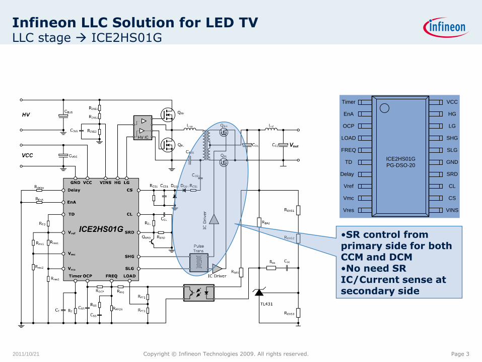
Page 3 Copyright © Infineon Technologies 2009. All rights reserved. 2011/10/21
Timer
ICE2HS01G
PG-DSO-20
LOAD
FREQ
TD
OCP
EnA
VINS
Vmc
SRD
CL
SLG
GND
LG
SHG
VCC
HG
CS
Delay
Vres
Vref
•SR control from primary side for both CCM and DCM •No need SR IC/Current sense at secondary side
Infineon LLC Solution for LED TV LLC stage ICE2HS01G

Page 4 Copyright © Infineon Technologies 2009. All rights reserved. 2011/10/21
Timer
ICE2HS01G
PG-DSO-20
LOAD
FREQ
TD
OCP
EnA
VINS
Vmc
SRD
CL
SLG
GND
LG
SHG
VCC
HG
CS
Delay
Vres
VrefAccurate set of frequency and deadtime
Infineon LLC Solution for LED TV LLC stage ICE2HS01G

Page 5 Copyright © Infineon Technologies 2009. All rights reserved. 2011/10/21
Timer
ICE2HS01G
PG-DSO-20
LOAD
FREQ
TD
OCP
EnA
VINS
Vmc
SRD
CL
SLG
GND
LG
SHG
VCC
HG
CS
Delay
Vres
Vref
brownout
OCP
OLP
Latch
Infineon LLC Solution for LED TV LLC stage ICE2HS01G

Page 6 Copyright © Infineon Technologies 2009. All rights reserved. 2011/10/21
S1-N
/ V
0
50
100
150
200
250
300
350
400
I(T
X2-3
1)
/ A
0
10
20
30
40
50
Time/mSecs 5uSecs/div
8.2 8.205 8.21 8.215 8.22 8.225
A
-3
-2
-1
0
1
2
0.2 0.3 0.4 0.5 0.6 0.7 0.8 0.9 1 1.1 1.2 1.30.8
0.85
0.91
0.96
1.01
1.07
1.12
1.17
1.23
1.28
1.33
1.39
1.44
1.49
1.55
1.6
G 0.2( )
G 0.238( )
G 0.3( )
G 0.345( )
G 0.585( )
G 0.765( )
G 1.0( )
Line
S1-N
/ V
0
50
100
150
200
250
300
350
400
I(T
X2-3
1)
/ A
0
5
10
15
20
25
30
Time/mSecs 2uSecs/div
8.41 8.412 8.414 8.416 8.418 8.42 8.422 8.424 8.426 8.428 8.43
A
-2
-1.5
-1
-0.5
0
0.5
1
1.5
Infineon LLC Solution for LED TV LLC stage ICE2HS01G

Page 7 Copyright © Infineon Technologies 2009. All rights reserved. 2011/10/21
Novel SR operation mode with various protections
LLC can designed at resonant frequency highest achievable efficiency
Reliable operation of SR Easy design
Control SR from primary controller No need of SR IC, low system cost
Tight tolerance control Feasibility for mass production
Accurate setting of switching frequency and dead time
Simple system design
optimized system efficiency
Various protections
OTP, OLP, OCP, Latch-off Enable Easy system design, short design cycle
Infineon LLC Solution for LED TV LLC stage ICE2HS01G

Page 8 Copyright © Infineon Technologies 2009. All rights reserved.
300W Evaluation board with ICE2HS01G System Design spec.
Main Input voltage: 315Vdc~420Vdc
Output: 12V/25A
Main Tran.: PQ3230 PC95
Resonant Choke: RM10 PC95
Pulse Tran.: EE13 PC44
Auxiliary input: 15V/50mA for IC
Primary MOSFET: IPA60R199CP
Secondary SR MOSFET: SPP015N04N G
Efficiency: 97% at 50% load
12/20/2010

Page 9 Copyright © Infineon Technologies 2009. All rights reserved.
300W Evaluation board with ICE2HS01G Main board schematics
12/20/2010
Page

Page 10 Copyright © Infineon Technologies 2009. All rights reserved.
300W Evaluation board with ICE2HS01G Control board schematics
12/20/2010

Page 11 Copyright © Infineon Technologies 2009. All rights reserved. 3 Jan 2011
Infineon Integrated Power IC (CoolSET® F3R80 DIP-7)
Vo
T2 CoolSET®-F3R80 IC
AC
~
DC
PWM IC CoolMOS C3
CoolSET®
ICE3XRxx80JZ DIP-7

Page 12 Copyright © Infineon Technologies 2009. All rights reserved. 3 Jan 2011
Naming System (Nomenclature) of CoolSET® -F3R80
ICE 3 A R 06 80 J Z
Divided by 10 (80 x 10 = 800V)

Page 13 Copyright © Infineon Technologies 2009. All rights reserved. 3 Jan 2011
ICE3XRxx80JZ – Product Highlights
PG-DIP7 package
BiCMOS technology provide higher Vcc voltage
800V avalanche rugged CoolMOS® with built-in startup Cell
65/100kHz Fixed Switching Frequency with frequency jitter
Enhanced Active Burst Mode for Lowest Standby Power with
Lower output ripple ( smaller burst on/off control voltage; 0.3V )
Selectable enter burst level ( 4 levels )
Adjustable brownout feature to provide robust control in application
Built-in 10ms soft start
Propagation delay compensation to provide accurate power control between low line and high line
Frequency jitter mode, soft gate driving and 50Ω gate turn on resistor to enhance EMI performance
Built-in 20ms and extendable Blanking Window for over load protection
Auto-Restart protection
Vcc Overvoltage, Overload, Open Loop, Vcc Undervoltage & Short Optocoupler, Over temperature (with 50°C hysteresis), External auto-restart enable pin
Pb-free lead plating; RoHS compilant

Page 14 Copyright © Infineon Technologies 2009. All rights reserved. 3 Jan 2011
Package : PG-DIP7
Package & Pin Configuration
1
7
8
4
3
2
5
GNDBBA
FBB
CS
VCC
n.c. Drain
Pin Symbol Function
1 BBA Brownout, extended Blanking time & Auto-restart enable
2 FBB FeedBack and Burst entry/exit control
3 CS Current Sense/800V CoolMOS® Source
4 n.c Not connected
5 Drain 800V CoolMOS®Drain
6 - (no pin)
7 Vcc Controller Supply Voltage
8 GND Controller Ground

Page 15 Copyright © Infineon Technologies 2009. All rights reserved. 3 Jan 2011
Block diagram
Internal Bias Voltage
Reference
Oscillator
Duty Cycle
max
x3.25
Current Limiting
PWM OP
Current Mode
Soft Start
RFB
Power Management
CBK
CVCC
85 ... 270 VACCBulk
+
Converter
DC Output
VOUT
PWM
Comparator
C30.9V
C44.5V
Gate
Driver
0.75
Clock
RSense
10k
D1C6a
3.2V
C5VFB_burst C10
R
S
Q
&
G7
&
G5
&
G9
CS
GND
C7
C8
FBB
PWM
Section
Control Unit
FF1
C12
LEB
220ns
25k
2pF
5.0V
1pF
Propagation-Delay
Compensation
5.0V
Undervoltage Lockout
Vcsth
-
ICE3XRxx80JZ / CoolSET®-F3R80 ( Brownout & Jitter Mode )
Snubber
VCC Drain
CoolMOS®
Startup Cell
C6b
3.5V&
G11
0.6V
10.5V
17V
#1
# : optional external components;
#1 : CBK is used to extend the Blanking Time
#2 : RBO1 & RBO2 are used for brownout feature; RBO1 tie to Vcc if no brownout feature
#3 : TAE is used to enable the external Auto-restart feature
Freq. jitter
20ms
Blanking
Time
Soft-Start
Comparator
Auto-restart
Enable
Signal
TAE
#3
CFB
BBA
Propagation-Delay
Compensation-Burst
Vcsth_burst
Burst
detect and
select
VFB_burstVcs_burst
RBO1
RBO2
#2
Power-Down
Reset
S2
Counter
C11
&G1
Spike
Blanking
30μs
4.5V
1
G8
C134.0V
20ms Blanking Time
Active Burst
Mode
Auto
Restart
Mode
Ichg_BO
S3
C14
0.9V
Brownout
mode
Ichg_EB
S1
5.0V
C120.5V
VCC
Thermal
Shutdown
Tj >130°CSoft
Start
Block
C90.4V
LEB
180ns
S4
G10
&
or
G13
#2
500 CT1
C2Vcc
VCC
25.5V
120μs
Blanking
Time

Page 16 Copyright © Infineon Technologies 2009. All rights reserved. 3 Jan 2011
Evaluation Board Circuit Diagram 12V 30W (Vin= 85Vac ~ 282Vac) using ICE3AR0680JZ
Enable BrownOut, EBO : Add R18, R19, R1100 and delete R17;
Disable BrownOut, DBO : Add R17 and delete R18, R19 and R100;
EBO and DBO would not happen at the same time.

Page 17 Copyright © Infineon Technologies 2009. All rights reserved. 3 Jan 2011
Stanby Power @ no-load versus AC Line Input Voltage
97.9575.06
57.0249.29
40.9235.57
34.7333.7131.8323.88
38.82 46.54
0
20
40
60
80
100
85 115 150 180 230 282
AC Line Input Voltage [ Vac ]
Inp
ut
Po
we
r [
mW
]
Po = 0W(Enable Broownout) Po=0W(Disable Brownout)
Standby Input Power at 0W and 0.5W load – using Yokogawa WT210 in integration timer mode
Standby Power Efficiency @ 0.5W
79.49
82.34
84.77 84.51
80.9878.71
74.40
82.42
70
75
80
85
90
0.5 1.0 2.0 3.0
Output power [ W ]
Eff
icie
ncy [
% ]
Vin=115Vac Vin=230Vac
Standby Power @ 0.5W load versus AC Line Input Voltage
0.610.63 0.63
0.65
0.67
0.70
0.50
0.55
0.60
0.65
0.70
0.75
0.80
85 115 150 180 230 282
AC Line Input Voltage [ Vac ]
Inp
ut
Po
wer
[ W
]
Po=0.5W
Measurement based on demo board 30W 12V using ICE3AR0680JZ

Page 18 Copyright © Infineon Technologies 2009. All rights reserved. 3 Jan 2011
Standby power at different CFB for no load and 0.5W load
Pin (mW) Enable Brownout Pin (mW) Disable Brownout
85Vac 115Vac 150Vac 180Vac 230Vac 282Vac 85Vac 115Vac 150Vac 180Vac 230Vac 282Vac
CFB=6.8nF 37.34 42.48 49.79 59.34 78.94 99.96 32.94 34.21 36.19 38.99 44.89 56.26
CFB=1nF 36.55 41.29 50.83 56.23 76.35 96.54 32.56 33.48 36.42 38.86 43.83 55.79
CFB=330pF 36.46 41.95 49.02 57.73 76.53 98.93 33.19 34.63 36.19 38.73 44.58 55.42
CFB=100pF 108.57 104.48 105.77 114.59 128.02 149.37 97.52 80.17 87.36 88.81 92.49 100.84
Pin (W) Enable Brownout Pin (W) Disable Brownout
85Vac 115Vac 150Vac 180Vac 230Vac 282Vac 85Vac 115Vac 150Vac 180Vac 230Vac 282Vac
CFB=6.8nF 0..584 0.595 0.610 0.625 0.638 0.664 0.581 0.596 0.605 0.606 0.612 0.628
CFB=1nF 0.611 0.625 0.630 0.633 0.650 0.679 0.585 0.601 0.606 0.619 0.629 0.647
CFB=330pF 0.606 0.614 0.637 0.642 0.668 0.682 0.589 0.602 0.614 0.620 0.630 0.652
CFB=100pF 0.857 0.812 0.796 0.804 0.826 0.869 0.840 0.782 0.772 0.76 0.77 0.79
Input standby power at no load with different CFB
Input standby power at 0.5W load with different CFB
Measurement based on demo board 30W 12V using ICE3AR0680JZ

Page 19 Copyright © Infineon Technologies 2009. All rights reserved. 2011/10/21
Auxiliary converter ICE2QRxx80JZ
85 ~ 265 VAC
SnubberCbus
Dr1~Dr4
RCS
TL431
Optocoupler
Rb1
Rb2
Rc1
Cc1 Cc2
Rovs2
Rovs1
CVCC
DVCC
DO
CO
Lf
Cf VO
CPSStartup Cell
CoolSET®-Q1
Depl. CoolMOS®
Power Cell
Wp
Ws
WaRVCC
CZC RZC2 RZC1
Drain
Zero Crossing Block
Power Management
Cycle-by-Cycle
current limitation
Active Burst Mode
PWM controller
Current Mode Control
Protections
VCC
CS
Control Unit
ZC
FB
GND
800V/650V CoolMOS
Active burst mode for low standby power

Page 20 Copyright © Infineon Technologies 2009. All rights reserved. 2011/10/21
Cin
Vin
LP
Cd
+
Vds
-
Vout
Benefits:
• Lower switching losses & Higher efficiency
• Lower switching interference & Lower EMI
Vds
tTON
TOFF1
TOFF2
Infineon System Solution for Computing SMPS Auxiliary converter ICE2QRxx80JZ

Page 21 Copyright © Infineon Technologies 2009. All rights reserved. 2011/10/21

Page 22 Copyright © Infineon Technologies 2009. All rights reserved. 2011/10/21

Page 23 Copyright © Infineon Technologies 2009. All rights reserved.
SMPS IC’s at a glance Focus Product Portfolio
FF CoolSET
ICE3BR4765J ICE3BR1765J ICE3BR0665J
ICE3BR4765JZ ICE3BR1765JZ ICE3BR0665JZ
ICE3BR4765JG
ICE3BR2565JF ICE3BR1565JF ICE3BR1065JF ICE3BR0665JF
ICE3A1065ELJ ICE3A2065ELJ
ICE3AR4780JZ ICE3AR2280JZ ICE3AR0680JZ
FF PWM IC ICE3BS03LJG ICE3AS03LJG
QR CoolSET ICE2QR4765 ICE2QR1765 ICE2QR0665
QR PWM IC ICE2QS01 ICE2QS02G ICE2QS03 ICE2QS03G
Res LLC HB ICE1HS01G ICE2HS01G
CCM PFC IC
ICE2PCS01 ICE2PCS02 ICE2PCS03 ICE2PCS04 ICE2PCS05 ICE2PCS06
ICE2PCS01G ICE2PCS02G ICE2PCS03G ICE2PCS04G ICE2PCS05G ICE2PCS06G
ICE3PCS01G ICE3PCS02G ICE3PCS03G
PFC+TTF ICE1CS02 ICE1CS02G

Page 24 Copyright © Infineon Technologies 2009. All rights reserved. 2011/10/21
Thank you !!
Any question?
