innovative plasma chemistry solutions to enable … plasma chemistry solutions to enable atomic...
TRANSCRIPT

© 2014 IBM Corporation
IBM Research
Innovative Plasma Chemistry Solutions to Enable Atomic Scale Precision
Eric A. Joseph, John Arnold* and Sebastian Engelmann
IBM T.J. Watson Research Center, Yorktown Heights, NY
* IBM Research at Albany Nanotech, Albany, NY
© 2014 IBM Corporation
IBM Research | Silicon Science & Process Technology | ALET Workshop | April 2014
SEMATECH Atomic Layer Etch Workshop 2
Outline
Introduction and motivation for Atomic Scale Precision
History and Review of Atomic Layer Etch Approaches
Atomic Scale Precision with Alternative Etch Chemistries
Conclusions and Acknowledgements

© 2014 IBM Corporation
IBM Research | Silicon Science & Process Technology | ALET Workshop | April 2014
SEMATECH Atomic Layer Etch Workshop 3
Traditional Logic Scaling Challenges
Scaling of CMOS devices is reaching atomic scale limit
New materials and integration schemes are being evaluated and introduced to enable performance improvements
Poly/SiO2 gate stack
Metal/High K dielectric gate stack
John E. Kelly III – RPI Seminar, 2012
H. Iwai, Roadmap for 22 nm and beyond, J. Microelectronic Eng. March 2009

© 2014 IBM Corporation
IBM Research | Silicon Science & Process Technology | ALET Workshop | April 2014
SEMATECH Atomic Layer Etch Workshop 4
Motivation and Needs for Atomic Scale Precision
Deliver leading edge processing for 7nm node and beyond technology
• Aggressive feature sizes (< 20nm) & non-planar device geometries
Selectivity to atomically thin films and the introduction of new materials
C-Electronics Trigate Si Nanowire Device
Planar: PDSOI
Si
STISTI
BOX
n
+
nnFE
T
n
+
Si
STISTI
BOX
n
+
nnFE
T
n
+
SI InP
10 nmTiNn+-Ge n+-Ge
NiGe NiGe
Source DrainInGaAshigh-κ
InAlAs buffer
SiN
ZL
SI InP
10 nmTiNn+-Ge n+-Ge
NiGe NiGe
Source DrainInGaAshigh-κ
InAlAs buffer
SiN
ZL
III-V Device
PZT
M0-Pt
SiO2
M1Al
Al
PRM3
M4
PZT
M0-Pt
SiO2
M1Al
Al
PR
PZT
M0-Pt
SiO2
PZT
M0-Pt
SiO2
M1Al
Al
PRM3
M4
Piezo Device

© 2014 IBM Corporation
IBM Research | Silicon Science & Process Technology | ALET Workshop | April 2014
SEMATECH Atomic Layer Etch Workshop 5
Atomic Layer Deposition
Digital (nm/cycle) ; Surface Controlled
High accuracy ; Slow throughput
Key Attribute Conformality Picture: Cepheiden
M. Gutsche et al Future Fab Intl. Issue 14 (2/11/2003)

© 2014 IBM Corporation
IBM Research | Silicon Science & Process Technology | ALET Workshop | April 2014
SEMATECH Atomic Layer Etch Workshop 6
Requirements to Enable Atomic Layer Etch
Digital (nm/process)
Surface Controlled
High accuracy
Key Attribute Selectivity!
John E. Kelly III – RPI Seminar, 2012
© 2014 IBM Corporation
IBM Research | Silicon Science & Process Technology | ALET Workshop | April 2014
SEMATECH Atomic Layer Etch Workshop 7
History of ALE
Google Search ‘ALE Plasma’
Atmospheric Pressure
CxHyOz Chemistry!!
Multi-disciplinary (as expected)
IPA + SAKE
© 2014 IBM Corporation
IBM Research | Silicon Science & Process Technology | ALET Workshop | April 2014
SEMATECH Atomic Layer Etch Workshop 8
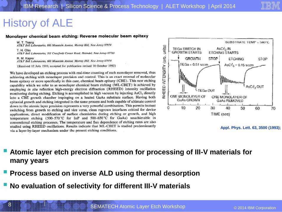
Atomic layer etch precision common for processing of III-V materials for
many years
Process based on inverse ALD using thermal desorption
No evaluation of selectivity for different III-V materials
History of ALE
Appl. Phys. Lett. 63, 3500 (1993);

© 2014 IBM Corporation
IBM Research | Silicon Science & Process Technology | ALET Workshop | April 2014
SEMATECH Atomic Layer Etch Workshop 9
Atomic Layer Etch by Anisotropic Wet Etch
Selective atomic scale
etch has been prevalent
for a considerable time
Etch capability defined by
crystallographic plane
orientation
Selectivity is chemistry
dependent! Prof. K. Sato, Dept. of Micro/Nano Systems Engineering, Nagoya University
(100) silicon wafer
(110) silicon wafer
© 2014 IBM Corporation
IBM Research | Silicon Science & Process Technology | ALET Workshop | April 2014
SEMATECH Atomic Layer Etch Workshop 10
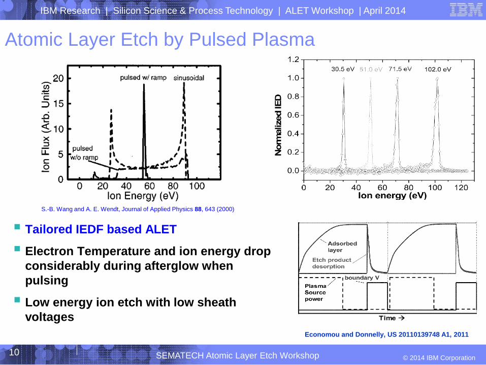
Atomic Layer Etch by Pulsed Plasma
Tailored IEDF based ALET
Electron Temperature and ion energy drop
considerably during afterglow when
pulsing
Low energy ion etch with low sheath
voltages
S.-B. Wang and A. E. Wendt, Journal of Applied Physics 88, 643 (2000)
Economou and Donnelly, US 20110139748 A1, 2011

© 2014 IBM Corporation
IBM Research | Silicon Science & Process Technology | ALET Workshop | April 2014
SEMATECH Atomic Layer Etch Workshop 11
Pulsed plasma enables formation of ion-ion plasmas in electronegative gases
Negative ion etch can proceed with less damage
Due to the mass balance between predominant positive and negative ions Cl2+ vs Cl-
Chemistry differences between negative and positive CFx species CF3+ vs F-
Enables Novel Chemistry capability
Kanakasabapthy, Ph.D. Dissertation, University of Texas at Dallas, 2001
Negative Ion Extraction for Atomic Scale Precision Plasma On Plasma Off Plasma On Plasma Off
A. Agarwal, S. Rauf, and K. Collins, JOURNAL OF APPLIED PHYSICS 112, 033303 (2012)
Temporal dynamics of electrons, positive and negative ion flux to the bottom electrode in a CF4/Cl2 50/50 plasma The positive ion flux is the sum of the fluxes of Cl2+, Cl+, CF3+, and CF2+, while the negative ion flux is the sum of the fluxes of Cl- and F-.

© 2014 IBM Corporation
IBM Research | Silicon Science & Process Technology | ALET Workshop | April 2014
SEMATECH Atomic Layer Etch Workshop 12
Atomic Layer Etch by Self-Limiting Processes
Surface Limited
Inverse ALD
• Cyclical process
• Adsorption / Desorption
• Requires multiple purges
Reactant limited
CW Argon plasma with
pulsed fluorocarbon
• Pulsed bias power to
initiate etch reaction
• Etch depth controlled by
ion energy and
fluorocarbon thickness
KEREN J. KANARIK et. al., Moving atomic layer etch from lab to fab, Solid State Technology 2014
Metlzer et. al., JVST B, 2014
Time
(c) (b) (a) C 4 F 8
Ar
Flow Rate
No Bias
Etching Active
Time
Passivation
Active Time
Bias
(c) (b) (a) C 4 F 8
Ar
Flow Rate
No Bias
Etching Active
Time
Passivation
Active Time
Bias
(a) (a)
No Bias

© 2014 IBM Corporation
IBM Research | Silicon Science & Process Technology | ALET Workshop | April 2014
SEMATECH Atomic Layer Etch Workshop 13
Outline
Introduction and motivation for Atomic Scale Precision
History and Review of Atomic Layer Etch Approaches
Atomic Scale Precision with Alternative Etch Chemistries
Conclusions and Acknowledgements
© 2014 IBM Corporation
IBM Research | Silicon Science & Process Technology | ALET Workshop | April 2014
SEMATECH Atomic Layer Etch Workshop 14
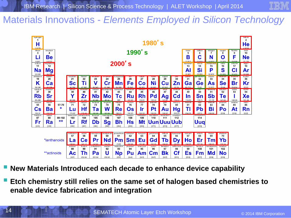
Materials Innovations - Elements Employed in Silicon Technology
1980’s
2000’s
1990’s
New Materials Introduced each decade to enhance device capability
Etch chemistry still relies on the same set of halogen based chemistries to
enable device fabrication and integration
© 2014 IBM Corporation
IBM Research | Silicon Science & Process Technology | ALET Workshop | April 2014
SEMATECH Atomic Layer Etch Workshop 15
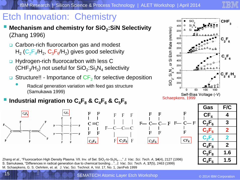
Mechanism and chemistry for SiO2:SiN Selectivity
(Zhang 1996)
Carbon-rich fluorocarbon gas and modest
H2 (C2F4/H2, C3F6/H2) gives good selectivity
Hydrogen-rich fluorocarbon with less C
(CHF3/H2) not useful for SiO2:Si3N4 selectivity
Structure!! - Importance of CF2 for selective deposition
• Radical generation variation with feed gas structure
(Samukawa 1999)
Industrial migration to C4F8 & C4F6 & C5F8
Zhang et al., “Fluorocarbon High Density Plasma. VII. Inv. of Sel. SiO2-to-Si3N4…,” J. Vac. Sci. Tech. A, 14(4), 2127 (1996)
S. Samukawa, “Differences in radical generation due to chemical bonding…”, J. Vac. Sci. Tech. A, 17(5), 2463 (1999)
M. Schaepkens, G. S. Oehrlein, et. al. J. Vac. Sci. Technol. A, Vol. 17, No. 1, Jan/Feb 1999
Gas F/C
CF4 4
C2F6 3
C3F6 2
C2F4 2
C4F8 2
C5F8 1.6
C4F6 1.5
Schaepkens, 1999
Etch Innovation: Chemistry

© 2014 IBM Corporation
IBM Research | Silicon Science & Process Technology | ALET Workshop | April 2014
SEMATECH Atomic Layer Etch Workshop 16
Mechanism and chemistry for SiO2:SiN Selectivity
(Zhang 1996)
Carbon-rich fluorocarbon gas and modest
H2 (C2F4/H2, C3F6/H2) gives good selectivity
Hydrogen-rich fluorocarbon with less C
(CHF3/H2) not useful for SiO2:Si3N4 selectivity
Structure!! - Importance of CF2 for selective deposition
• Radical generation variation with feed gas structure
(Samukawa 1999)
Industrial migration to C4F8 & C4F6 & C5F8
Zhang et al., “Fluorocarbon High Density Plasma. VII. Inv. of Sel. SiO2-to-Si3N4…,” J. Vac. Sci. Tech. A, 14(4), 2127 (1996)
S. Samukawa, “Differences in radical generation due to chemical bonding…”, J. Vac. Sci. Tech. A, 17(5), 2463 (1999)
M. Schaepkens, G. S. Oehrlein, et. al. J. Vac. Sci. Technol. A, Vol. 17, No. 1, Jan/Feb 1999
Gas F/C
CF4 4
C2F6 3
C3F6 2
C2F4 2
C4F8 2
C5F8 1.6
C4F6 1.5
Schaepkens, 1999
Etch Innovation: Chemistry
Inte
ns
ity (
a.u
.)
CF2
263 nm
C3
412 nmC2
516 nm
© 2014 IBM Corporation
IBM Research | Silicon Science & Process Technology | ALET Workshop | April 2014
SEMATECH Atomic Layer Etch Workshop 17
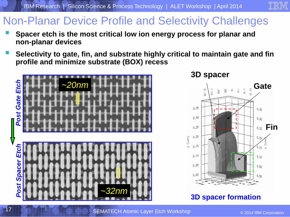
Spacer etch is the most critical low ion energy process for planar and non-planar devices
Selectivity to gate, fin, and substrate highly critical to maintain gate and fin profile and minimize substrate (BOX) recess
Non-Planar Device Profile and Selectivity Challenges
3D spacer formation
Gate
3D spacer
Fin Po
st
Gate
Etc
hP
ost
Sp
acer
Etc
h
~32nm
~20nm~20nm

© 2014 IBM Corporation
IBM Research | Silicon Science & Process Technology | ALET Workshop | April 2014
SEMATECH Atomic Layer Etch Workshop 18
Spacer Module & Atomic Precision
Spacer module considered most challenging, as all materials exposed to plasma remain on device
Module becomes even more challenging for novel device geometries (FinFET, Trigate, Nanowire)
Typical approach to enable processing has focused on alternating reactor configuration
First attempt to solve this issue from using a plasma chemistry approach
substrate
After spacer deposition
substrate
After spacer deposition
Traditional spacer process
substrate
Nitride thinning/
pull down
Si damage/
oxidation
After spacer etch
substrate
Nitride thinning/
pull down
Si damage/
oxidation
After spacer etch
Novel spacer process
substrate
Uniform
sidewall
coverageProtection by
FC deposit
After spacer etch
substrate
Uniform
sidewall
coverageProtection by
FC deposit
substrate
Uniform
sidewall
coverageProtection by
FC deposit
After spacer etch

© 2014 IBM Corporation
IBM Research | Silicon Science & Process Technology | ALET Workshop | April 2014
SEMATECH Atomic Layer Etch Workshop 19
Atomic Scale Precision with Novel ZEON Chemistry
0.0 0.5 1.0 1.5 2.0
0
10
20
30
40
50
60
Oxide
Nitride
Silicon
Etc
h r
ate
(n
m/m
in)
Fluorocarbon film thickness (nm)
Selective
nitride etching
Novel etch mechanism for selective nitride etch is achieved with ZEON gas
chemistry
Nitride etch rate favorably controlled by fluorocarbon reaction layer thickness
M. Schaepkens et al., J. Vac. Sci. Technol. A 17, 26 (1999)
0 1 2 3 4 5 6 7 8 0
100
200
300
400
500
Oxide
Nitride
Silicon
Etc
h R
ate
(nm
/min
)
Fluorocarbon Film Thickness (nm)
0 1 2 3 4 5 6 7 8 0
100
200
300
400
500
Oxide
Nitride
Silicon
Etc
h R
ate
(nm
/min
)
Fluorocarbon Film Thickness (nm)
Selective
oxide etching

© 2014 IBM Corporation
IBM Research | Silicon Science & Process Technology | ALET Workshop | April 2014
SEMATECH Atomic Layer Etch Workshop 20
ZEON SiN Spacer Process Performance
ZEON process has
better PDSOI Device
performance with
respect to HM and
spacer sidewall loss
Zeon gas process on
Trigate Devices shows
clean gate and desired
growth on Fin after
epitaxial growth
process
POR (CH3F/O2)
process shows
parasitic Si growth on
gate sidewall
POR
ZEON I
ZEON II
HM
PC
HKMG
Spacer
PDSOI Device
POR process Un-optimized Zeon gas process
Trigate Device
1.7
1.3
1.5
SOI loss
[nm]
ZEON II 0 0 4.5
ZEON I 2.5 0 4.3
POR process
4.4 0.2 6.8
Process SiN footing
[nm]
Spacer
loss [nm]
HM loss
[nm]
1.7
1.3
3.0
SOI loss
[nm]
ZEON II 0 0 4.5
ZEON I 2.5 0 4.3
POR process
4.4 0.2 6.8
Process SiN footing
[nm]
Spacer
loss [nm]
HM loss
[nm]

© 2014 IBM Corporation
IBM Research | Silicon Science & Process Technology | ALET Workshop | April 2014
SEMATECH Atomic Layer Etch Workshop 21
Post Spacer Deposition
Post Spacer Etch
ZEON SiN Spacer Process Performance
Si loss is reduced considerably with the addition
of optimized wet cleans, tailored to remove
polymer from selective etch
No longer a wet process to remove oxidized silicon
Pseudo atomic scale precision achieved

© 2014 IBM Corporation
IBM Research | Silicon Science & Process Technology | ALET Workshop | April 2014
SEMATECH Atomic Layer Etch Workshop 22
Post Spacer Deposition
Post Spacer Etch
ZEON SiN Spacer Process Performance
Pseudo atomic scale precision achieved
© 2014 IBM Corporation
IBM Research | Silicon Science & Process Technology | ALET Workshop | April 2014
SEMATECH Atomic Layer Etch Workshop 23
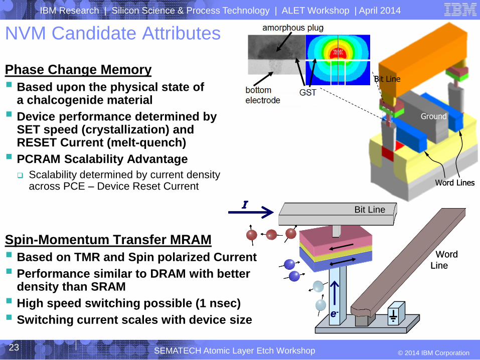
NVM Candidate Attributes
Phase Change Memory
Based upon the physical state of a chalcogenide material
Device performance determined by SET speed (crystallization) and RESET Current (melt-quench)
PCRAM Scalability Advantage
Scalability determined by current density across PCE – Device Reset Current
Spin-Momentum Transfer MRAM
Based on TMR and Spin polarized Current
Performance similar to DRAM with better density than SRAM
High speed switching possible (1 nsec)
Switching current scales with device size
Word
Line
I Bit Line
e-
Word
Line
II Bit Line
e-e-
SET
Bit Line
Word Lines
GroundSET
Bit Line
Word Lines
Ground
© 2014 IBM Corporation
IBM Research | Silicon Science & Process Technology | ALET Workshop | April 2014
SEMATECH Atomic Layer Etch Workshop 24
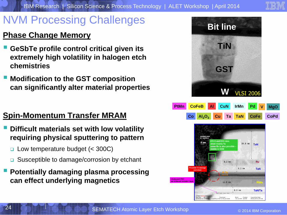
NVM Processing Challenges
Phase Change Memory
GeSbTe profile control critical given its
extremely high volatility in halogen etch
chemistries
Modification to the GST composition
can significantly alter material properties
Spin-Momentum Transfer MRAM
Difficult materials set with low volatility
requiring physical sputtering to pattern
Low temperature budget (< 300C)
Susceptible to damage/corrosion by etchant
Potentially damaging plasma processing
can effect underlying magnetics
PtMn
Co
CoFeB
CoFe
Al
Cu
CuN
Ta TaN
VPd
CoPdAl2O3
MgOIrMn
Bit line
W
GST
TiN
Bit line
W
GST
TiN
VLSI 2006
EELS and EDS data
show mostly Ta
some Ru is also possible –
visible in SEM
TaN
TaN
TaN/Ta
Ru
PtMn
AlOx
Possible TJ damage
and short
Likely post CMP
un-removed oxidation layer
TJ Stack Nominal Composition
Base layer AF Pinned layer Barrier Freelayer Cap and Hard Mask
50 TaN |20 Ta 175 38PtMn 5 CoFeB |14 70CF |7.5 Ru |24 CoFeB 7 Al / Ox POR 40 81NF 80TaN |100 Ru |700 TaN

© 2014 IBM Corporation
IBM Research | Silicon Science & Process Technology | ALET Workshop | April 2014
SEMATECH Atomic Layer Etch Workshop 25
Wafer 2, 7NGST
Wafer 9, 7NGST, etch step 1
Wafer 11, 7NGST, etch & clean
Wafer 12, 7NGST, etch & strip
Wafer 2, 7NGST
Wafer 9, 7NGST, etch step 1
Wafer 11, 7NGST, etch & clean
Wafer 12, 7NGST, etch & strip
Laser Reflectivity Data
Laser Reflectivity measurements used to determine (re)crystallization speed
Exposure to plasma chemistry significantly reduces speed by as much as three orders of magnitude
PCM: Effects of Processing on Crystallization Speed
As Deposited
Post Etch
Post Etch and Clean
Post Etch and Strip

© 2014 IBM Corporation
IBM Research | Silicon Science & Process Technology | ALET Workshop | April 2014
SEMATECH Atomic Layer Etch Workshop 26
Depth profiled XPS Analysis of partially etched GST reveals significant modification
Nitrogen, Antimony and Tellurium loss
Etch induced Modification ranges as much as 12nm in depth
X-ray absorption spectroscopy shows shifts in germanium absorption edge energy
Change in oxidation state: Ge-N replaced by Ge-O
Band Edge ShiftBand Edge Shift
0 2 4 6 8 10 12
0
5
10
15
20
25
Depth (nm)
Ato
mic
Fra
ction (
%)
Sb Metal
0 2 4 6 8 10 12
0
1
2
3
4
5
6
A
tom
ic F
ractio
n (
%) N
Depth (nm)
Characterization of Etch Induced PCM Material Modification

© 2014 IBM Corporation
IBM Research | Silicon Science & Process Technology | ALET Workshop | April 2014
SEMATECH Atomic Layer Etch Workshop 27
Effect of Cladding / Cap Layer
Data from literature demonstrates the effect of cap materials on the crystallization properties of GST films
Due to modification of the incubation time, changes in nucleation and potentially thermal conductivity effects
GST thickness also significantly effects crystallization time as well!
We can conclude that etch damage creates a thinner film (obvious) and leaves an oxide (GeO) atop the GST, behaving as a cladding layer.
Result is a significant increase in crystallization time and FCC HCP transition temperature
H-Y Cheng et al, NVMTS 2009 H-Y Cheng et al, NVMTS 2009

© 2014 IBM Corporation
IBM Research | Silicon Science & Process Technology | ALET Workshop | April 2014
SEMATECH Atomic Layer Etch Workshop 28
Repair / Removal of Modified Layer
Etch damage repair technique demonstrated on patterned structures
Technique is highly selective to undamaged N:GST
No Difference observed after 100% overetch
0s 30s 60s 120s
TiN
N:GST N:GST
TiN
Can original stoichiometry of the N:GST film be recovered after etch?
YES
© 2014 IBM Corporation
IBM Research | Silicon Science & Process Technology | ALET Workshop | April 2014
SEMATECH Atomic Layer Etch Workshop 29
Conclusions
Various methods to perform large scale ALE are currently under development
Key attribute for ALE is still selectivity and will rely heavily on plasma chemistry
to achieve atomic scale precision
A new ZEON etch chemistry has been developed for SiN etch applications
which exhibits Atomic Scale Precision based on a novel selective fluorocarbon
deposition mechanism
Use of the novel ZEON chemistry also demonstrates high selectivity to C-based materials
enabling use in SiN patterning applications with low LER/LWR
Plasma chemistry critical for complex Non-Volatile Memory materials as
selective volatilization and plasma induced material modification effect device
performance
Critical understanding needed to develop damage-free ALE
© 2014 IBM Corporation
IBM Research | Silicon Science & Process Technology | ALET Workshop | April 2014
SEMATECH Atomic Layer Etch Workshop 30
Acknowledgements
All results shown have been produced in the Microelectronics Research
Laboratory (MRL) at the T.J. Watson Research Center, Yorktown Heights
Authors would like to thank our etch colleagues in East Fishkill and Albany
Nanotech for helpful discussions and providing wafers.
Authors would also like to thank the MRL staff & MRL management for support
of this work