integrated cmos class-e power amplifier for self …lrf.ufsc.br/files/2012/07/pid4305889.pdf ·...
TRANSCRIPT
Integrated CMOS Class-E Power Amplifier forSelf-Sustaining Wireless Power Transfer system
Arturo Fajardo Jaimes∗†∗ Department of Electronics Engineering
Pontifical Xavierian University, Bogota, ColombiaEmail: [email protected]
Fernando Rangel de Sousa †† Radiofrequency Laboratory
Department of Electrical and Electronics EngineeringFederal University of Santa Catarina (UFSC), Florianopolis, Brazil
Email: [email protected]
Abstract—In this paper is proposed a methodology for de-signing a CMOS class-E PA used to drive an inductive link.In order to satisfy the operating conditions imposed by the PAspecifications and the available technology, a differential class-E PA with split slab inductor and high level of integration wasboth designed and simulated. The proposed methodology uses theanalytical solution of the ideal class-E PA equations as the firstpoint of an iterative procedure for solving the optimization of thePA. Further, the proposed design set solve the trade-off betweenON-resistance and gate capacitance of the switches, resulting inthe optimal choice of the power transistors width for a class-EPA with finite DC-feed inductance. In the post-layout simulation,the PAE of the PA was 45.7% when 20.7 dBm.
Keywords—Class-E, power amplifier, power efficiency, wirelesspower transfer.
I. INTRODUCTION
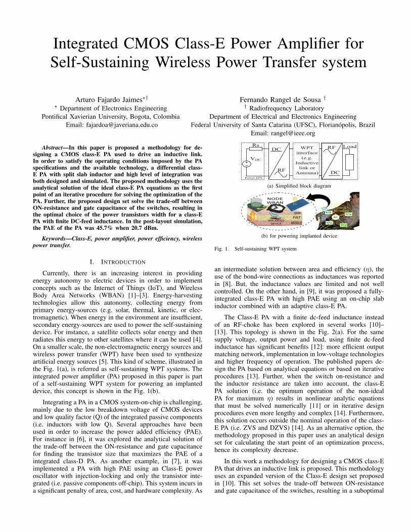
Currently, there is an increasing interest in providingenergy autonomy to electric devices in order to implementconcepts such as the Internet of Things (IoT), and WirelessBody Area Networks (WBAN) [1]–[3]. Energy-harvestingtechnologies allow this autonomy, collecting energy fromprimary energy-sources (e.g. solar, thermal, kinetic, or elec-tromagnetic). When energy in the environment are insufficient,secondary energy-sources are used to power the self-sustainingdevice. For instance, a satellite collects solar energy and thenradiates this energy to other satellites where it can be used [4].On a smaller scale, the non-electromagnetic energy sources andwireless power transfer (WPT) have been used to synthesizeartificial energy sources [5]. This kind of scheme, illustrated inthe Fig. 1(a), is referred as self-sustaining WPT systems. Theintegrated power amplifier (PA) proposed in this paper is partof a self-sustaining WPT system for powering an implanteddevice, this concept is shown in the Fig. 1(b).
Integrating a PA in a CMOS system-on-chip is challenging,mainly due to the low breakdown voltage of CMOS devicesand low quality factor (Q) of the integrated passive components(i.e. inductors with low Q). Several approaches have beenused in order to increase the power added efficiency (PAE).For instance in [6], it was explored the analytical solution ofthe trade-off between the ON-resistance and gate capacitancefor finding the transistor size that maximizes the PAE of aintegrated class-D PA. As another example, in [7], it wasimplemented a PA with high PAE using an Class-E poweroscillator with injection-locking and only the transistor inte-grated (i.e. passive components off-chip). This system incurs ina significant penalty of area, cost, and hardware complexity. As
VDC
LoadDC
RF
WPT
interface
(e.g.
Inductive
link or
Antenna) DC
RFRs
Power EPS
(a) Simplified block diagram
N1aH1
N1cN1d
SKIN
MUSCLE
FAT
N1b
IMPLANTED DEVICE
NODE WBAN
WBAN NETWORK
(b) for powering implanted device
Fig. 1. Self-sustaining WPT system
an intermediate solution between area and efficiency (𝜂), theuse of the bond-wire connections as inductances was reportedin [8]. But, the inductance values are limited and not wellcontrolled. On the other hand, in [9], it was proposed a fully-integrated class-E PA with high PAE using an on-chip slabinductor combined with an adaptive class-E PA.
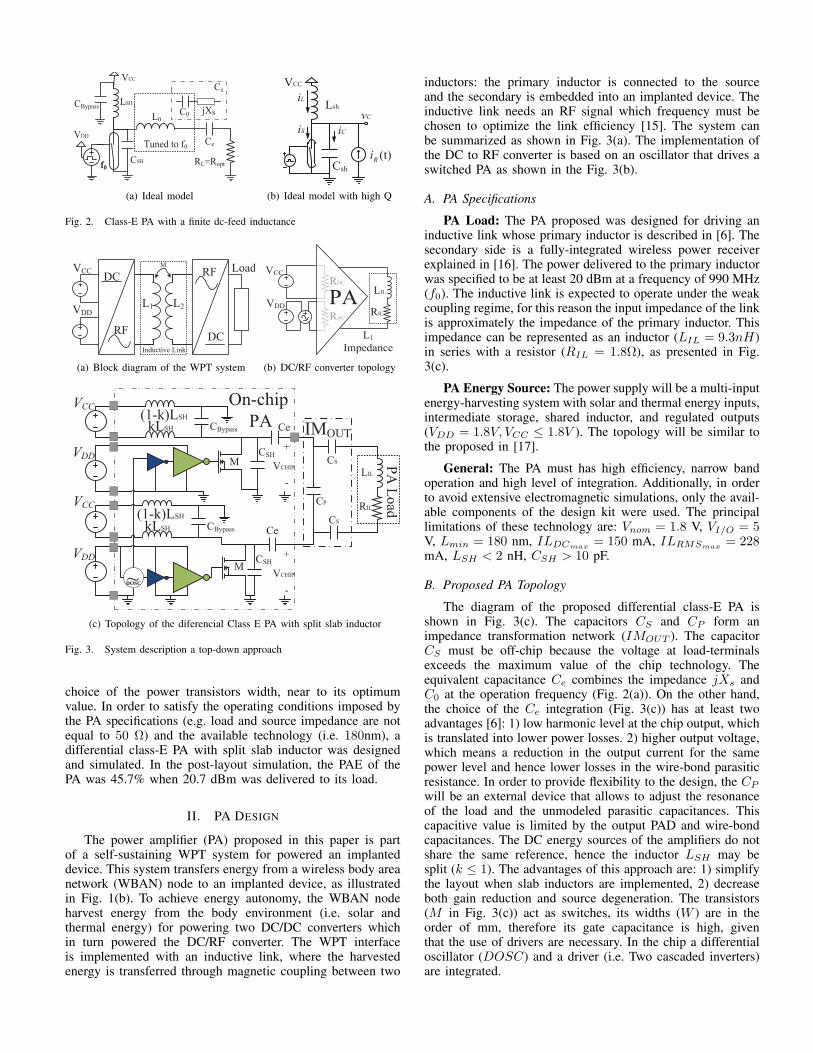
The Class-E PA with a finite dc-feed inductance insteadof an RF-choke has been explored in several works [10]–[13]. This topology is shown in the Fig. 2(a). For the samesupply voltage, output power and load, using finite dc-feedinductance has significant benefits [12]: more efficient outputmatching network, implementation in low-voltage technologiesand higher frequency of operation. The published papers de-sign the PA based on analytical equations or based on iterativeprocedures [13]. Further, when the switch on-resistance andthe inductor resistance are taken into account, the class-EPA solution (i.e. the optimum operation of the non-idealPA for maximum 𝜂) results in nonlinear analytic equationsthat must be solved numerically [11] or in iterative designprocedures even more lengthy and complex [14]. Furthermore,this solution occurs outside the nominal operation of the class-E PA (i.e. ZVS and DZVS) [14]. As an alternative option, themethodology proposed in this paper uses an analytical designset for calculating the start point of an optimization process,hence its complexity decrease.
In this work a methodology for designing a CMOS class-EPA that drives an inductive link is proposed. This methodologyuses an expanded version of the Class-E design set proposedin [10]. This set solves the trade-off between ON-resistanceand gate capacitance of the switches, resulting in a suboptimal
RL=RoptCSH
LSH
L0
f0
VCC
VDD
Tuned to f0
jXSCBypass
Ce
C0
Ce
(a) Ideal model
Csh
Lsh
(t)Ri
VCCiL
iCiSvC
(b) Ideal model with high Q
Fig. 2. Class-E PA with a finite dc-feed inductance
VCCM
VDD
LoadDC
RF
L1 L2
Inductive LinkDC
RF
(a) Block diagram of the WPT system
RDC
RAC
PAVCC
VDDRIL
L1 Impedance
LIL
(b) DC/RF converter topology
RIL
LIL
CP
CS
CS
Ce
CSH
On-chip PA
PA Load
Ce
CSH
kLSH
M+
-
(1-k)LSH
VCHIP~DOSC
M
kLSH(1-k)LSH
VCC
VDD
VCC
VDD
+
-VCHIP
IMOUT
CBypass
CBypass
(c) Topology of the diferencial Class E PA with split slab inductor
Fig. 3. System description a top-down approach
choice of the power transistors width, near to its optimumvalue. In order to satisfy the operating conditions imposed bythe PA specifications (e.g. load and source impedance are notequal to 50 Ω) and the available technology (i.e. 180nm), adifferential class-E PA with split slab inductor was designedand simulated. In the post-layout simulation, the PAE of thePA was 45.7% when 20.7 dBm was delivered to its load.
II. PA DESIGN
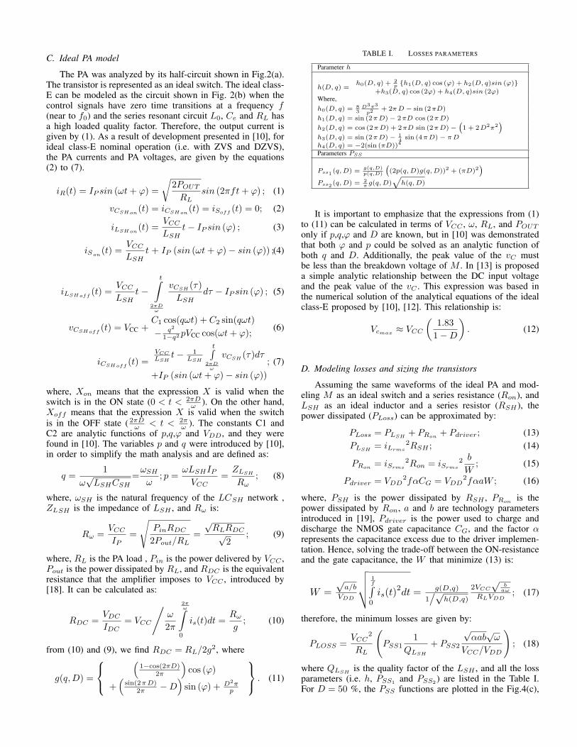
The power amplifier (PA) proposed in this paper is partof a self-sustaining WPT system for powered an implanteddevice. This system transfers energy from a wireless body areanetwork (WBAN) node to an implanted device, as illustratedin Fig. 1(b). To achieve energy autonomy, the WBAN nodeharvest energy from the body environment (i.e. solar andthermal energy) for powering two DC/DC converters whichin turn powered the DC/RF converter. The WPT interfaceis implemented with an inductive link, where the harvestedenergy is transferred through magnetic coupling between two
inductors: the primary inductor is connected to the sourceand the secondary is embedded into an implanted device. Theinductive link needs an RF signal which frequency must bechosen to optimize the link efficiency [15]. The system canbe summarized as shown in Fig. 3(a). The implementation ofthe DC to RF converter is based on an oscillator that drives aswitched PA as shown in the Fig. 3(b).
A. PA Specifications
PA Load: The PA proposed was designed for driving aninductive link whose primary inductor is described in [6]. Thesecondary side is a fully-integrated wireless power receiverexplained in [16]. The power delivered to the primary inductorwas specified to be at least 20 dBm at a frequency of 990 MHz(𝑓0). The inductive link is expected to operate under the weakcoupling regime, for this reason the input impedance of the linkis approximately the impedance of the primary inductor. Thisimpedance can be represented as an inductor (𝐿𝐼𝐿 = 9.3𝑛𝐻)in series with a resistor (𝑅𝐼𝐿 = 1.8Ω), as presented in Fig.3(c).
PA Energy Source: The power supply will be a multi-inputenergy-harvesting system with solar and thermal energy inputs,intermediate storage, shared inductor, and regulated outputs(𝑉𝐷𝐷 = 1.8𝑉, 𝑉𝐶𝐶 ≤ 1.8𝑉 ). The topology will be similar tothe proposed in [17].
General: The PA must has high efficiency, narrow bandoperation and high level of integration. Additionally, in orderto avoid extensive electromagnetic simulations, only the avail-able components of the design kit were used. The principallimitations of these technology are: 𝑉𝑛𝑜𝑚 = 1.8 V, 𝑉𝐼/𝑂 = 5V, 𝐿𝑚𝑖𝑛 = 180 nm, 𝐼𝐿𝐷𝐶𝑚𝑎𝑥
= 150 mA, 𝐼𝐿𝑅𝑀𝑆𝑚𝑎𝑥 = 228mA, 𝐿𝑆𝐻 < 2 nH, 𝐶𝑆𝐻 > 10 pF.
B. Proposed PA Topology
The diagram of the proposed differential class-E PA isshown in Fig. 3(c). The capacitors 𝐶𝑆 and 𝐶𝑃 form animpedance transformation network (𝐼𝑀𝑂𝑈𝑇 ). The capacitor𝐶𝑆 must be off-chip because the voltage at load-terminalsexceeds the maximum value of the chip technology. Theequivalent capacitance 𝐶𝑒 combines the impedance 𝑗𝑋𝑠 and𝐶0 at the operation frequency (Fig. 2(a)). On the other hand,the choice of the 𝐶𝑒 integration (Fig. 3(c)) has at least twoadvantages [6]: 1) low harmonic level at the chip output, whichis translated into lower power losses. 2) higher output voltage,which means a reduction in the output current for the samepower level and hence lower losses in the wire-bond parasiticresistance. In order to provide flexibility to the design, the 𝐶𝑃
will be an external device that allows to adjust the resonanceof the load and the unmodeled parasitic capacitances. Thiscapacitive value is limited by the output PAD and wire-bondcapacitances. The DC energy sources of the amplifiers do notshare the same reference, hence the inductor 𝐿𝑆𝐻 may besplit (𝑘 ≤ 1). The advantages of this approach are: 1) simplifythe layout when slab inductors are implemented, 2) decreaseboth gain reduction and source degeneration. The transistors(𝑀 in Fig. 3(c)) act as switches, its widths (𝑊 ) are in theorder of mm, therefore its gate capacitance is high, giventhat the use of drivers are necessary. In the chip a differentialoscillator (𝐷𝑂𝑆𝐶) and a driver (i.e. Two cascaded inverters)are integrated.
C. Ideal PA model
The PA was analyzed by its half-circuit shown in Fig.2(a).The transistor is represented as an ideal switch. The ideal class-E can be modeled as the circuit shown in Fig. 2(b) when thecontrol signals have zero time transitions at a frequency 𝑓(near to 𝑓0) and the series resonant circuit 𝐿0, 𝐶𝑒 and 𝑅𝐿 hasa high loaded quality factor. Therefore, the output current isgiven by (1). As a result of development presented in [10], forideal class-E nominal operation (i.e. with ZVS and DZVS),the PA currents and PA voltages, are given by the equations(2) to (7).
𝑖𝑅(𝑡) = 𝐼𝑃 𝑠𝑖𝑛 (𝜔𝑡+ 𝜑) =
√2𝑃𝑂𝑈𝑇
𝑅𝐿𝑠𝑖𝑛 (2𝜋𝑓𝑡+ 𝜑) ; (1)
𝑣𝐶𝑆𝐻𝑜𝑛(𝑡) = 𝑖𝐶𝑆𝐻𝑜𝑛
(𝑡) = 𝑖𝑆𝑜𝑓𝑓 (𝑡) = 0; (2)
𝑖𝐿𝑆𝐻𝑜𝑛(𝑡) =
𝑉𝐶𝐶
𝐿𝑆𝐻𝑡− 𝐼𝑃 𝑠𝑖𝑛 (𝜑) ; (3)
𝑖𝑆𝑜𝑛(𝑡) =𝑉𝐶𝐶
𝐿𝑆𝐻𝑡 + 𝐼𝑃 (𝑠𝑖𝑛 (𝜔𝑡+ 𝜑)− 𝑠𝑖𝑛 (𝜑)) ;(4)
𝑖𝐿𝑆𝐻𝑜𝑓𝑓(𝑡) =
𝑉𝐶𝐶
𝐿𝑆𝐻𝑡 −
𝑡∫2𝜋𝐷𝜔
𝑣𝐶𝑆𝐻 (𝜏)
𝐿𝑆𝐻𝑑𝜏 − 𝐼𝑃 𝑠𝑖𝑛 (𝜑) ; (5)
𝑣𝐶𝑆𝐻𝑜𝑓𝑓(𝑡) = 𝑉CC +
𝐶1 cos(𝑞𝜔𝑡) + 𝐶2 sin(𝑞𝜔𝑡)
− 𝑞2
1−𝑞2 𝑝𝑉CC cos(𝜔𝑡+ 𝜑);(6)
𝑖𝐶𝑆𝐻𝑜𝑓𝑓(𝑡) =
𝑉𝐶𝐶𝐿𝑆𝐻
𝑡− 1𝐿𝑆𝐻
𝑡∫2𝜋𝐷𝜔
𝑣𝐶𝑆𝐻 (𝜏)𝑑𝜏
+𝐼𝑃 (𝑠𝑖𝑛 (𝜔𝑡+ 𝜑)− 𝑠𝑖𝑛 (𝜑))
; (7)
where, 𝑋𝑜𝑛 means that the expression 𝑋 is valid when theswitch is in the ON state (0 < 𝑡 < 2𝜋𝐷
𝜔 ). On the other hand,𝑋𝑜𝑓𝑓 means that the expression 𝑋 is valid when the switchis in the OFF state ( 2𝜋𝐷𝜔 < 𝑡 < 2𝜋
𝜔 ). The constants C1 andC2 are analytic functions of 𝑝,𝑞,𝜑 and 𝑉𝐷𝐷, and they werefound in [10]. The variables 𝑝 and 𝑞 were introduced by [10],in order to simplify the math analysis and are defined as:
𝑞 =1
𝜔√𝐿𝑆𝐻𝐶𝑆𝐻
=𝜔𝑆𝐻
𝜔; 𝑝 =
𝜔𝐿𝑆𝐻𝐼𝑃𝑉𝐶𝐶
=𝑍𝐿𝑆𝐻
𝑅𝜔; (8)
where, 𝜔𝑆𝐻 is the natural frequency of the 𝐿𝐶𝑆𝐻 network ,𝑍𝐿𝑆𝐻 is the impedance of 𝐿𝑆𝐻 , and 𝑅𝜔 is:
𝑅𝜔 =𝑉𝐶𝐶
𝐼𝑃=
√𝑃𝑖𝑛𝑅𝐷𝐶
2𝑃𝑜𝑢𝑡/𝑅𝐿=
√𝑅𝐿𝑅𝐷𝐶√
2; (9)
where, 𝑅𝐿 is the PA load , 𝑃𝑖𝑛 is the power delivered by 𝑉𝐶𝐶 ,𝑃𝑜𝑢𝑡 is the power dissipated by 𝑅𝐿, and 𝑅𝐷𝐶 is the equivalentresistance that the amplifier imposes to 𝑉𝐶𝐶 , introduced by[18]. It can be calculated as:
𝑅𝐷𝐶 =𝑉𝐷𝐶
𝐼𝐷𝐶= 𝑉𝐶𝐶
/𝜔
2𝜋
2𝜋𝜔∫
0
𝑖𝑠(𝑡)𝑑𝑡 =𝑅𝜔
𝑔; (10)
from (10) and (9), we find 𝑅𝐷𝐶 = 𝑅𝐿/2𝑔2, where
𝑔(𝑞,𝐷) =
⎧⎨⎩
(1−cos(2𝜋𝐷)
2𝜋
)cos (𝜑)
+(
sin(2𝜋𝐷)2𝜋 −𝐷
)sin (𝜑) + 𝐷2𝜋
𝑝
⎫⎬⎭ . (11)
TABLE I. LOSSES PARAMETERS
Parameter ℎ
ℎ(𝐷, 𝑞) =ℎ0(𝐷, 𝑞) + 2
𝑝 {ℎ1(𝐷, 𝑞) cos (𝜑) + ℎ2(𝐷, 𝑞)𝑠𝑖𝑛 (𝜑)}+ℎ3(𝐷, 𝑞) cos (2𝜑) + ℎ4(𝐷, 𝑞)𝑠𝑖𝑛 (2𝜑)
Where,
ℎ0(𝐷, 𝑞) = 83𝐷3𝜋3
𝑝2+ 2𝜋𝐷 − sin (2𝜋𝐷)
ℎ1(𝐷, 𝑞) = sin (2𝜋𝐷) − 2𝜋𝐷 cos (2𝜋𝐷)
ℎ2(𝐷, 𝑞) = cos (2𝜋𝐷) + 2𝜋𝐷 sin (2𝜋𝐷) −(1 + 2𝐷2𝜋2
)ℎ3(𝐷, 𝑞) = sin (2𝜋𝐷) − 1
4 sin (4𝜋𝐷) − 𝜋𝐷ℎ4(𝐷, 𝑞) = −2(sin (𝜋𝐷))4
Parameters 𝑃𝑆𝑆
𝑃𝑠𝑠1 (𝑞,𝐷) =𝑔(𝑞,𝐷)𝑝(𝑞,𝐷)
((2𝑝(𝑞,𝐷)𝑔(𝑞,𝐷))2 + (𝜋𝐷)2
)𝑃𝑠𝑠2 (𝑞,𝐷) = 2
𝜋 𝑔(𝑞,𝐷)√
ℎ(𝑞,𝐷)
It is important to emphasize that the expressions from (1)to (11) can be calculated in terms of 𝑉𝐶𝐶 , 𝜔, 𝑅𝐿, and 𝑃𝑂𝑈𝑇
only if 𝑝,𝑞,𝜑 and 𝐷 are known, but in [10] was demonstratedthat both 𝜑 and 𝑝 could be solved as an analytic function ofboth 𝑞 and 𝐷. Additionally, the peak value of the 𝑣𝐶 mustbe less than the breakdown voltage of 𝑀 . In [13] is proposeda simple analytic relationship between the DC input voltageand the peak value of the 𝑣𝐶 . This expression was based inthe numerical solution of the analytical equations of the idealclass-E proposed by [10], [12]. This relationship is:
𝑉𝑐𝑚𝑎𝑥 ≈ 𝑉𝐶𝐶
(1.83
1−𝐷
). (12)
D. Modeling losses and sizing the transistors
Assuming the same waveforms of the ideal PA and mod-eling 𝑀 as an ideal switch and a series resistance (𝑅𝑜𝑛), and𝐿𝑆𝐻 as an ideal inductor and a series resistor (𝑅𝑆𝐻 ), thepower dissipated (𝑃𝐿𝑜𝑠𝑠) can be approximated by:
𝑃𝐿𝑜𝑠𝑠 = 𝑃𝐿𝑆𝐻 + 𝑃𝑅𝑜𝑛 + 𝑃𝑑𝑟𝑖𝑣𝑒𝑟; (13)𝑃𝐿𝑆𝐻 = 𝑖𝐿𝑟𝑚𝑠
2𝑅𝑆𝐻 ; (14)
𝑃𝑅𝑜𝑛 = 𝑖𝑆𝑟𝑚𝑠2𝑅𝑜𝑛 = 𝑖𝑆𝑟𝑚𝑠
2 𝑏
𝑊; (15)
𝑃𝑑𝑟𝑖𝑣𝑒𝑟 = 𝑉𝐷𝐷2𝑓𝛼𝐶𝐺 = 𝑉𝐷𝐷
2𝑓𝛼𝑎𝑊 ; (16)
where, 𝑃𝑆𝐻 is the power dissipated by 𝑅𝑆𝐻 , 𝑃𝑅𝑜𝑛 is thepower dissipated by 𝑅𝑜𝑛, 𝑎 and 𝑏 are technology parametersintroduced in [19], 𝑃𝑑𝑟𝑖𝑣𝑒𝑟 is the power used to charge anddischarge the NMOS gate capacitance 𝐶𝐺, and the factor 𝛼represents the capacitance excess due to the driver implemen-tation. Hence, solving the trade-off between the ON-resistanceand the gate capacitance, the 𝑊 that minimize (13) is:
𝑊 =
√𝑎/𝑏
𝑉𝐷𝐷
√√√⎷ 1𝑓∫0
𝑖𝑠(𝑡)2𝑑𝑡 = 𝑔(𝐷,𝑞)
1/√
ℎ(𝐷,𝑞)
2𝑉𝐶𝐶√
𝑏𝑎𝜔
𝑅𝐿𝑉𝐷𝐷; (17)
therefore, the minimum losses are given by:
𝑃𝐿𝑂𝑆𝑆 =𝑉𝐶𝐶
2
𝑅𝐿
(𝑃𝑆𝑆1
1
𝑄𝐿𝑆𝐻
+ 𝑃𝑆𝑆2
√𝛼𝑎𝑏
√𝜔
𝑉𝐶𝐶/𝑉𝐷𝐷
); (18)
where 𝑄𝐿𝑆𝐻 is the quality factor of the 𝐿𝑆𝐻 , and all the lossparameters (i.e. ℎ, 𝑃𝑆𝑆1
and 𝑃𝑆𝑆2) are listed in the Table I.
For 𝐷 = 50 %, the 𝑃𝑆𝑆 functions are plotted in the Fig.4(c),
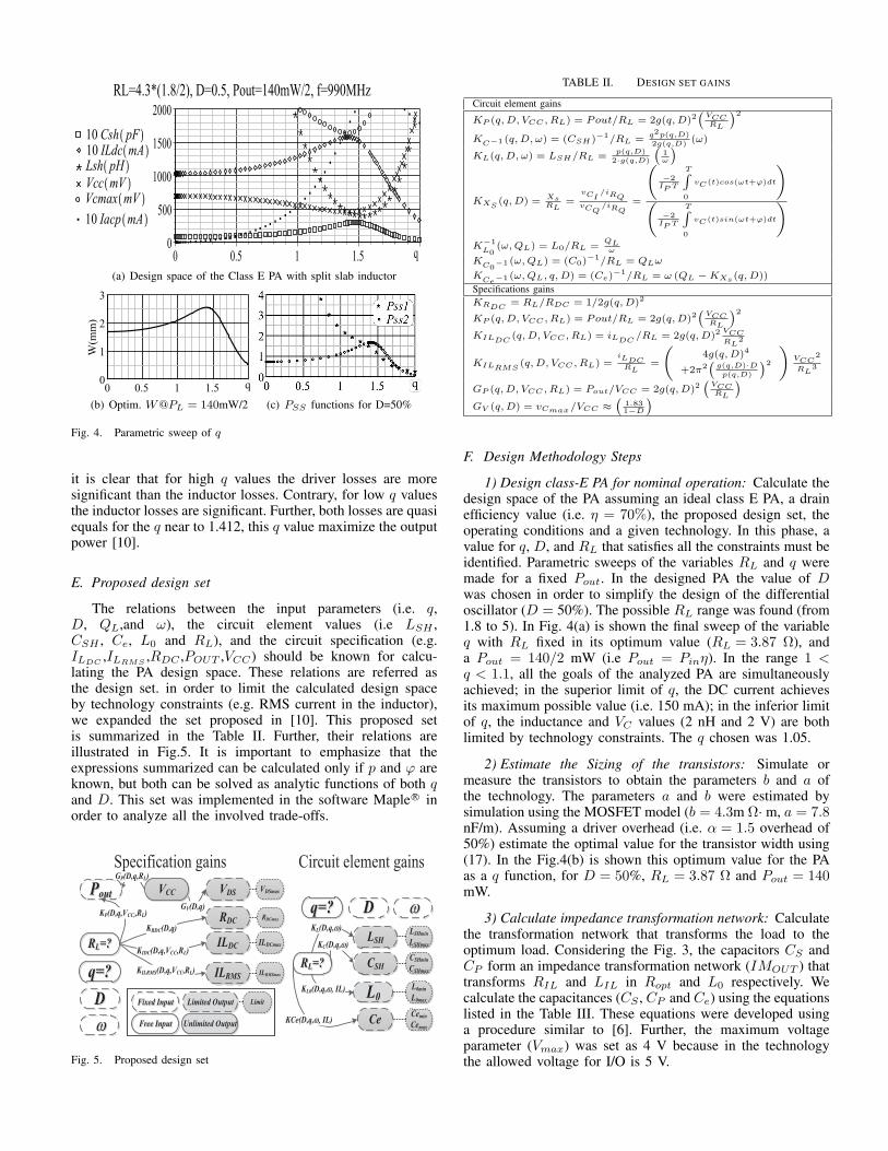
(a) Design space of the Class E PA with split slab inductor
(b) Optim. 𝑊@𝑃𝐿 = 140mW/2 (c) 𝑃𝑆𝑆 functions for D=50%
Fig. 4. Parametric sweep of 𝑞
it is clear that for high 𝑞 values the driver losses are moresignificant than the inductor losses. Contrary, for low 𝑞 valuesthe inductor losses are significant. Further, both losses are quasiequals for the 𝑞 near to 1.412, this 𝑞 value maximize the outputpower [10].
E. Proposed design set
The relations between the input parameters (i.e. 𝑞,𝐷, 𝑄𝐿,and 𝜔), the circuit element values (i.e 𝐿𝑆𝐻 ,𝐶𝑆𝐻 , 𝐶𝑒, 𝐿0 and 𝑅𝐿), and the circuit specification (e.g.𝐼𝐿𝐷𝐶 ,𝐼𝐿𝑅𝑀𝑆
,𝑅𝐷𝐶 ,𝑃𝑂𝑈𝑇 ,𝑉𝐶𝐶) should be known for calcu-lating the PA design space. These relations are referred asthe design set. in order to limit the calculated design spaceby technology constraints (e.g. RMS current in the inductor),we expanded the set proposed in [10]. This proposed setis summarized in the Table II. Further, their relations areillustrated in Fig.5. It is important to emphasize that theexpressions summarized can be calculated only if 𝑝 and 𝜑 areknown, but both can be solved as analytic functions of both 𝑞and 𝐷. This set was implemented in the software Maple R⃝ inorder to analyze all the involved trade-offs.
ILDCLSH
CSH
L0
VDS
ILRMSmaxq=?q=?DD
KL(D,q, )
KC(D,q, )
GV(D,q)
VDSmax
GP(D,q,RL)
ILDCmaxKIDC(D,q,VCC,RL)
PoutPout VCC
RL=?RL=?
ILRMS
LSHminLSHmax
CSHminCSHmax
CeminCemax
Ce
RL=?RL=?
Fixed Input Fixed Input
KILRMS(D,q,VCC,RL)
Free Input Free Input
Limited Output
Unlimited Output
Limit
q=?q=? DD
Specification gains Circuit element gains
KL0(D,q, IL)
RDC RDCmax
KRDC(D,q)
KCe(D,q, IL)
L0minL0max
KP(D,q,VCC,,RL)
Fig. 5. Proposed design set
TABLE II. DESIGN SET GAINS
Circuit element gains
𝐾𝑃 (𝑞,𝐷, 𝑉𝐶𝐶 , 𝑅𝐿) = 𝑃𝑜𝑢𝑡/𝑅𝐿 = 2𝑔(𝑞,𝐷)2(𝑉𝐶𝐶𝑅𝐿
)2𝐾𝐶−1 (𝑞,𝐷, 𝜔) = (𝐶𝑆𝐻)−1/𝑅𝐿 =
𝑞2𝑝(𝑞,𝐷)2𝑔(𝑞,𝐷)
(𝜔)
𝐾𝐿(𝑞,𝐷, 𝜔) = 𝐿𝑆𝐻/𝑅𝐿 =𝑝(𝑞,𝐷)
2⋅𝑔(𝑞,𝐷)
(1𝜔
)
𝐾𝑋𝑆(𝑞,𝐷) = 𝑋𝑠
𝑅𝐿=
𝑣𝐶𝐼/𝑖𝑅𝑄
𝑣𝐶𝑄/𝑖𝑅𝑄
=
(−2𝐼𝑃 𝑇
𝑇∫0
𝑣𝐶 (𝑡)𝑐𝑜𝑠(𝜔𝑡+𝜑)𝑑𝑡
)(
−2𝐼𝑃 𝑇
𝑇∫0
𝑣𝐶 (𝑡)𝑠𝑖𝑛(𝜔𝑡+𝜑)𝑑𝑡
)𝐾−1𝐿0
(𝜔,𝑄𝐿) = 𝐿0/𝑅𝐿 =𝑄𝐿𝜔
𝐾𝐶0−1 (𝜔,𝑄𝐿) = (𝐶0)
−1/𝑅𝐿 = 𝑄𝐿𝜔
𝐾𝐶𝑒−1 (𝜔,𝑄𝐿, 𝑞,𝐷) = (𝐶𝑒)−1/𝑅𝐿 = 𝜔 (𝑄𝐿 −𝐾𝑋𝑠 (𝑞,𝐷))
Specifications gains𝐾𝑅𝐷𝐶
= 𝑅𝐿/𝑅𝐷𝐶 = 1/2𝑔(𝑞,𝐷)2
𝐾𝑃 (𝑞,𝐷, 𝑉𝐶𝐶 , 𝑅𝐿) = 𝑃𝑜𝑢𝑡/𝑅𝐿 = 2𝑔(𝑞,𝐷)2(𝑉𝐶𝐶𝑅𝐿
)2𝐾𝐼𝐿𝐷𝐶
(𝑞,𝐷, 𝑉𝐶𝐶 , 𝑅𝐿) = 𝑖𝐿𝐷𝐶 /𝑅𝐿 = 2𝑔(𝑞,𝐷)2𝑉𝐶𝐶𝑅𝐿
2
𝐾𝐼𝐿𝑅𝑀𝑆(𝑞,𝐷, 𝑉𝐶𝐶 , 𝑅𝐿) =
𝑖𝐿𝐷𝐶𝑅𝐿
=
(4𝑔(𝑞,𝐷)4
+2𝜋2(𝑔(𝑞,𝐷)⋅𝐷𝑝(𝑞,𝐷)
)2 ) 𝑉𝐶𝐶2
𝑅𝐿3
𝐺𝑃 (𝑞,𝐷, 𝑉𝐶𝐶 , 𝑅𝐿) = 𝑃𝑜𝑢𝑡/𝑉𝐶𝐶 = 2𝑔(𝑞,𝐷)2(𝑉𝐶𝐶𝑅𝐿
)𝐺𝑉 (𝑞,𝐷) = 𝑣𝐶𝑚𝑎𝑥/𝑉𝐶𝐶 ≈
(1.831−𝐷)
F. Design Methodology Steps
1) Design class-E PA for nominal operation: Calculate thedesign space of the PA assuming an ideal class E PA, a drainefficiency value (i.e. 𝜂 = 70%), the proposed design set, theoperating conditions and a given technology. In this phase, avalue for 𝑞, 𝐷, and 𝑅𝐿 that satisfies all the constraints must beidentified. Parametric sweeps of the variables 𝑅𝐿 and 𝑞 weremade for a fixed 𝑃𝑜𝑢𝑡. In the designed PA the value of 𝐷was chosen in order to simplify the design of the differentialoscillator (𝐷 = 50%). The possible 𝑅𝐿 range was found (from1.8 to 5). In Fig. 4(a) is shown the final sweep of the variable𝑞 with 𝑅𝐿 fixed in its optimum value (𝑅𝐿 = 3.87 Ω), anda 𝑃𝑜𝑢𝑡 = 140/2 mW (i.e 𝑃𝑜𝑢𝑡 = 𝑃𝑖𝑛𝜂). In the range 1 <𝑞 < 1.1, all the goals of the analyzed PA are simultaneouslyachieved; in the superior limit of 𝑞, the DC current achievesits maximum possible value (i.e. 150 mA); in the inferior limitof 𝑞, the inductance and 𝑉𝐶 values (2 nH and 2 V) are bothlimited by technology constraints. The 𝑞 chosen was 1.05.
2) Estimate the Sizing of the transistors: Simulate ormeasure the transistors to obtain the parameters 𝑏 and 𝑎 ofthe technology. The parameters 𝑎 and 𝑏 were estimated bysimulation using the MOSFET model (𝑏 = 4.3m Ω⋅ m, 𝑎 = 7.8nF/m). Assuming a driver overhead (i.e. 𝛼 = 1.5 overhead of50%) estimate the optimal value for the transistor width using(17). In the Fig.4(b) is shown this optimum value for the PAas a 𝑞 function, for 𝐷 = 50%, 𝑅𝐿 = 3.87 Ω and 𝑃𝑜𝑢𝑡 = 140mW.
3) Calculate impedance transformation network: Calculatethe transformation network that transforms the load to theoptimum load. Considering the Fig. 3, the capacitors 𝐶𝑆 and𝐶𝑃 form an impedance transformation network (𝐼𝑀𝑂𝑈𝑇 ) thattransforms 𝑅𝐼𝐿 and 𝐿𝐼𝐿 in 𝑅𝑜𝑝𝑡 and 𝐿0 respectively. Wecalculate the capacitances (𝐶𝑆 , 𝐶𝑃 and 𝐶𝑒) using the equationslisted in the Table III. These equations were developed usinga procedure similar to [6]. Further, the maximum voltageparameter (𝑉𝑚𝑎𝑥) was set as 4 V because in the technologythe allowed voltage for I/O is 5 V.
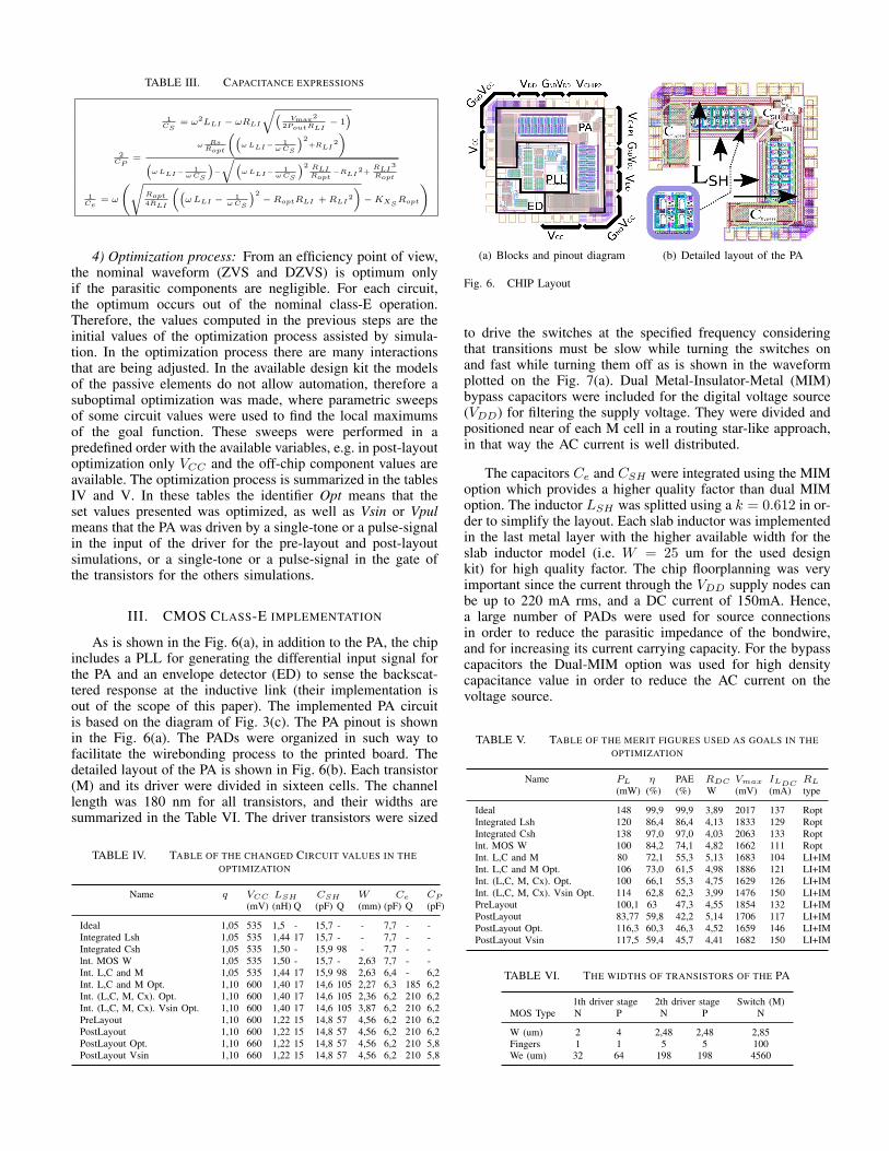
TABLE III. CAPACITANCE EXPRESSIONS
1𝐶𝑆
= 𝜔2𝐿𝐿𝐼 − 𝜔𝑅𝐿𝐼
√(𝑉max2
2𝑃𝑜𝑢𝑡𝑅𝐿𝐼− 1)
2𝐶𝑃
=
𝜔 𝑅𝑠𝑅𝑜𝑝𝑡
((𝜔𝐿𝐿𝐼− 1
𝜔𝐶𝑆
)2+𝑅𝐿𝐼
2
)(𝜔𝐿𝐿𝐼− 1
𝜔𝐶𝑆
)−√(
𝜔𝐿𝐿𝐼− 1𝜔𝐶𝑆
)2 𝑅𝐿𝐼𝑅𝑜𝑝𝑡
−𝑅𝐿𝐼2+𝑅𝐿𝐼
3
𝑅𝑜𝑝𝑡
1𝐶𝑒
= 𝜔
(√𝑅𝑜𝑝𝑡4𝑅𝐿𝐼
((𝜔𝐿𝐿𝐼 − 1
𝜔𝐶𝑆
)2 − 𝑅𝑜𝑝𝑡𝑅𝐿𝐼 + 𝑅𝐿𝐼2)
−𝐾𝑋𝑆𝑅𝑜𝑝𝑡
)
4) Optimization process: From an efficiency point of view,the nominal waveform (ZVS and DZVS) is optimum onlyif the parasitic components are negligible. For each circuit,the optimum occurs out of the nominal class-E operation.Therefore, the values computed in the previous steps are theinitial values of the optimization process assisted by simula-tion. In the optimization process there are many interactionsthat are being adjusted. In the available design kit the modelsof the passive elements do not allow automation, therefore asuboptimal optimization was made, where parametric sweepsof some circuit values were used to find the local maximumsof the goal function. These sweeps were performed in apredefined order with the available variables, e.g. in post-layoutoptimization only 𝑉𝐶𝐶 and the off-chip component values areavailable. The optimization process is summarized in the tablesIV and V. In these tables the identifier Opt means that theset values presented was optimized, as well as Vsin or Vpulmeans that the PA was driven by a single-tone or a pulse-signalin the input of the driver for the pre-layout and post-layoutsimulations, or a single-tone or a pulse-signal in the gate ofthe transistors for the others simulations.
III. CMOS CLASS-E IMPLEMENTATION
As is shown in the Fig. 6(a), in addition to the PA, the chipincludes a PLL for generating the differential input signal forthe PA and an envelope detector (ED) to sense the backscat-tered response at the inductive link (their implementation isout of the scope of this paper). The implemented PA circuitis based on the diagram of Fig. 3(c). The PA pinout is shownin the Fig. 6(a). The PADs were organized in such way tofacilitate the wirebonding process to the printed board. Thedetailed layout of the PA is shown in Fig. 6(b). Each transistor(M) and its driver were divided in sixteen cells. The channellength was 180 nm for all transistors, and their widths aresummarized in the Table VI. The driver transistors were sized
TABLE IV. TABLE OF THE CHANGED CIRCUIT VALUES IN THE
OPTIMIZATION
Name 𝑞 𝑉𝐶𝐶 𝐿𝑆𝐻 𝐶𝑆𝐻 𝑊 𝐶𝑒 𝐶𝑃(mV) (nH) Q (pF) Q (mm) (pF) Q (pF)
Ideal 1,05 535 1,5 - 15,7 - - 7,7 - -Integrated Lsh 1,05 535 1,44 17 15,7 - - 7,7 - -Integrated Csh 1,05 535 1,50 - 15,9 98 - 7,7 - -lnt. MOS W 1,05 535 1,50 - 15,7 - 2,63 7,7 - -Int. L,C and M 1,05 535 1,44 17 15,9 98 2,63 6,4 - 6,2Int. L,C and M Opt. 1,10 600 1,40 17 14,6 105 2,27 6,3 185 6,2Int. (L,C, M, Cx). Opt. 1,10 600 1,40 17 14,6 105 2,36 6,2 210 6,2Int. (L,C, M, Cx). Vsin Opt. 1,10 600 1,40 17 14,6 105 3,87 6,2 210 6,2PreLayout 1,10 600 1,22 15 14,8 57 4,56 6,2 210 6,2PostLayout 1,10 600 1,22 15 14,8 57 4,56 6,2 210 6,2PostLayout Opt. 1,10 660 1,22 15 14,8 57 4,56 6,2 210 5,8PostLayout Vsin 1,10 660 1,22 15 14,8 57 4,56 6,2 210 5,8
(a) Blocks and pinout diagram
LSH
(b) Detailed layout of the PA
Fig. 6. CHIP Layout
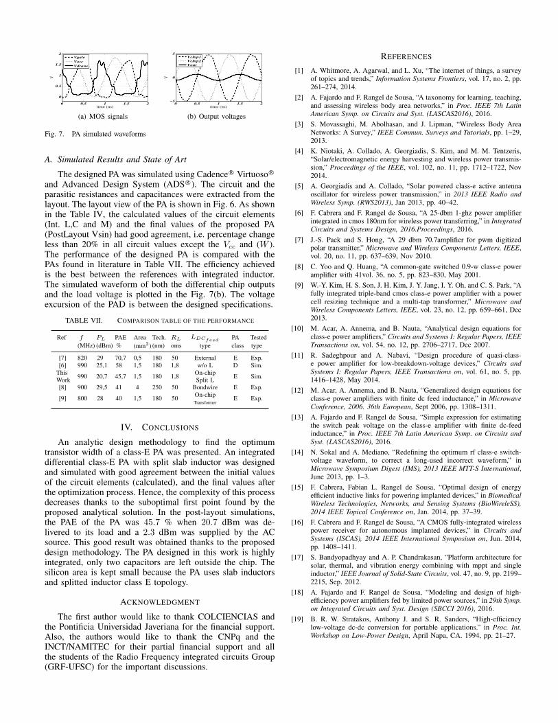
to drive the switches at the specified frequency consideringthat transitions must be slow while turning the switches onand fast while turning them off as is shown in the waveformplotted on the Fig. 7(a). Dual Metal-Insulator-Metal (MIM)bypass capacitors were included for the digital voltage source(𝑉𝐷𝐷) for filtering the supply voltage. They were divided andpositioned near of each M cell in a routing star-like approach,in that way the AC current is well distributed.
The capacitors 𝐶𝑒 and 𝐶𝑆𝐻 were integrated using the MIMoption which provides a higher quality factor than dual MIMoption. The inductor 𝐿𝑆𝐻 was splitted using a 𝑘 = 0.612 in or-der to simplify the layout. Each slab inductor was implementedin the last metal layer with the higher available width for theslab inductor model (i.e. 𝑊 = 25 um for the used designkit) for high quality factor. The chip floorplanning was veryimportant since the current through the 𝑉𝐷𝐷 supply nodes canbe up to 220 mA rms, and a DC current of 150mA. Hence,a large number of PADs were used for source connectionsin order to reduce the parasitic impedance of the bondwire,and for increasing its current carrying capacity. For the bypasscapacitors the Dual-MIM option was used for high densitycapacitance value in order to reduce the AC current on thevoltage source.
TABLE V. TABLE OF THE MERIT FIGURES USED AS GOALS IN THE
OPTIMIZATION
Name 𝑃𝐿 𝜂 PAE 𝑅𝐷𝐶 𝑉𝑚𝑎𝑥 𝐼𝐿𝐷𝐶 𝑅𝐿(mW) (%) (%) W (mV) (mA) type
Ideal 148 99,9 99,9 3,89 2017 137 RoptIntegrated Lsh 120 86,4 86,4 4,13 1833 129 RoptIntegrated Csh 138 97,0 97,0 4,03 2063 133 Roptlnt. MOS W 100 84,2 74,1 4,82 1662 111 RoptInt. L,C and M 80 72,1 55,3 5,13 1683 104 LI+IMInt. L,C and M Opt. 106 73,0 61,5 4,98 1886 121 LI+IMInt. (L,C, M, Cx). Opt. 100 66,1 55,3 4,75 1629 126 LI+IMInt. (L,C, M, Cx). Vsin Opt. 114 62,8 62,3 3,99 1476 150 LI+IMPreLayout 100,1 63 47,3 4,55 1854 132 LI+IMPostLayout 83,77 59,8 42,2 5,14 1706 117 LI+IMPostLayout Opt. 116,3 60,3 46,3 4,52 1659 146 LI+IMPostLayout Vsin 117,5 59,4 45,7 4,41 1682 150 LI+IM
TABLE VI. THE WIDTHS OF TRANSISTORS OF THE PA
1th driver stage 2th driver stage Switch (M)MOS Type N P N P N
W (um) 2 4 2,48 2,48 2,85Fingers 1 1 5 5 100We (um) 32 64 198 198 4560
0 0.5 1 1.5 2
0
0.5
1
1.5
2
time (ns)
V
VgateVoscVdrane
(a) MOS signals
0 0.5 1 1.5 2−5
0
5
time (ns)
V
Vchip1Vchip2Vout
(b) Output voltages
Fig. 7. PA simulated waveforms
A. Simulated Results and State of Art
The designed PA was simulated using Cadence R⃝ Virtuoso R⃝
and Advanced Design System (ADS R⃝). The circuit and theparasitic resistances and capacitances were extracted from thelayout. The layout view of the PA is shown in Fig. 6. As shownin the Table IV, the calculated values of the circuit elements(Int. L,C and M) and the final values of the proposed PA(PostLayout Vsin) had good agreement, i.e. percentage changeless than 20% in all circuit values except the 𝑉𝑐𝑐 and (𝑊 ).The performance of the designed PA is compared with thePAs found in literature in Table VII. The efficiency achievedis the best between the references with integrated inductor.The simulated waveform of both the differential chip outputsand the load voltage is plotted in the Fig. 7(b). The voltageexcursion of the PAD is between the designed specifications.
TABLE VII. COMPARISON TABLE OF THE PERFORMANCE
Ref 𝑓 𝑃𝐿 PAE Area Tech. 𝑅𝐿 𝐿𝐷𝐶𝑓𝑒𝑒𝑑 PA Tested(MHz) (dBm) % (mm2) (nm) oms type class type
[7] 820 29 70,7 0,5 180 50 External E Exp.[6] 990 25,1 58 1,5 180 1,8 w/o L D Sim.
ThisWork
990 20,7 45,7 1,5 180 1,8On-chipSplit L
E Sim.
[8] 900 29,5 41 4 250 50 Bondwire E Exp.
[9] 800 28 40 1,5 180 50On-chipTransformer
E Exp.
IV. CONCLUSIONS
An analytic design methodology to find the optimumtransistor width of a class-E PA was presented. An integrateddifferential class-E PA with split slab inductor was designedand simulated with good agreement between the initial valuesof the circuit elements (calculated), and the final values afterthe optimization process. Hence, the complexity of this processdecreases thanks to the suboptimal first point found by theproposed analytical solution. In the post-layout simulations,the PAE of the PA was 45.7 % when 20.7 dBm was de-livered to its load and a 2.3 dBm was supplied by the ACsource. This good result was obtained thanks to the proposeddesign methodology. The PA designed in this work is highlyintegrated, only two capacitors are left outside the chip. Thesilicon area is kept small because the PA uses slab inductorsand splitted inductor class E topology.
ACKNOWLEDGMENT
The first author would like to thank COLCIENCIAS andthe Pontificia Universidad Javeriana for the financial support.Also, the authors would like to thank the CNPq and theINCT/NAMITEC for their partial financial support and allthe students of the Radio Frequency integrated circuits Group(GRF-UFSC) for the important discussions.
REFERENCES
[1] A. Whitmore, A. Agarwal, and L. Xu, “The internet of things, a surveyof topics and trends,” Information Systems Frontiers, vol. 17, no. 2, pp.261–274, 2014.
[2] A. Fajardo and F. Rangel de Sousa, “A taxonomy for learning, teaching,and assessing wireless body area networks,” in Proc. IEEE 7th LatinAmerican Symp. on Circuits and Syst. (LASCAS2016), 2016.
[3] S. Movassaghi, M. Abolhasan, and J. Lipman, “Wireless Body AreaNetworks: A Survey,” IEEE Commun. Surveys and Tutorials, pp. 1–29,2013.
[4] K. Niotaki, A. Collado, A. Georgiadis, S. Kim, and M. M. Tentzeris,“Solar/electromagnetic energy harvesting and wireless power transmis-sion,” Proceedings of the IEEE, vol. 102, no. 11, pp. 1712–1722, Nov2014.
[5] A. Georgiadis and A. Collado, “Solar powered class-e active antennaoscillator for wireless power transmission,” in 2013 IEEE Radio andWireless Symp. (RWS2013), Jan 2013, pp. 40–42.
[6] F. Cabrera and F. Rangel de Sousa, “A 25-dbm 1-ghz power amplifierintegrated in cmos 180nm for wireless power transferring,” in IntegratedCircuits and Systems Design, 2016.Proceedings, 2016.
[7] J.-S. Paek and S. Hong, “A 29 dbm 70.7amplifier for pwm digitizedpolar transmitter,” Microwave and Wireless Components Letters, IEEE,vol. 20, no. 11, pp. 637–639, Nov 2010.
[8] C. Yoo and Q. Huang, “A common-gate switched 0.9-w class-e poweramplifier with 41vol. 36, no. 5, pp. 823–830, May 2001.
[9] W.-Y. Kim, H. S. Son, J. H. Kim, J. Y. Jang, I. Y. Oh, and C. S. Park, “Afully integrated triple-band cmos class-e power amplifier with a powercell resizing technique and a multi-tap transformer,” Microwave andWireless Components Letters, IEEE, vol. 23, no. 12, pp. 659–661, Dec2013.
[10] M. Acar, A. Annema, and B. Nauta, “Analytical design equations forclass-e power amplifiers,” Circuits and Systems I: Regular Papers, IEEETransactions on, vol. 54, no. 12, pp. 2706–2717, Dec 2007.
[11] R. Sadeghpour and A. Nabavi, “Design procedure of quasi-class-e power amplifier for low-breakdown-voltage devices,” Circuits andSystems I: Regular Papers, IEEE Transactions on, vol. 61, no. 5, pp.1416–1428, May 2014.
[12] M. Acar, A. Annema, and B. Nauta, “Generalized design equations forclass-e power amplifiers with finite dc feed inductance,” in MicrowaveConference, 2006. 36th European, Sept 2006, pp. 1308–1311.
[13] A. Fajardo and F. Rangel de Sousa, “Simple expression for estimatingthe switch peak voltage on the class-e amplifier with finite dc-feedinductance,” in Proc. IEEE 7th Latin American Symp. on Circuits andSyst. (LASCAS2016), 2016.
[14] N. Sokal and A. Mediano, “Redefining the optimum rf class-e switch-voltage waveform, to correct a long-used incorrect waveform,” inMicrowave Symposium Digest (IMS), 2013 IEEE MTT-S International,June 2013, pp. 1–3.
[15] F. Cabrera, Fabian L. Rangel de Sousa, “Optimal design of energyefficient inductive links for powering implanted devices,” in BiomedicalWireless Technologies, Networks, and Sensing Systems (BioWireleSS),2014 IEEE Topical Conference on, Jan. 2014, pp. 37–39.
[16] F. Cabrera and F. Rangel de Sousa, “A CMOS fully-integrated wirelesspower receiver for autonomous implanted devices,” in Circuits andSystems (ISCAS), 2014 IEEE International Symposium on, Jun. 2014,pp. 1408–1411.
[17] S. Bandyopadhyay and A. P. Chandrakasan, “Platform architecture forsolar, thermal, and vibration energy combining with mppt and singleinductor,” IEEE Journal of Solid-State Circuits, vol. 47, no. 9, pp. 2199–2215, Sep. 2012.
[18] A. Fajardo and F. Rangel de Sousa, “Modeling and design of high-efficiency power amplifiers fed by limited power sources,” in 29th Symp.on Integrated Circuits and Syst. Design (SBCCI 2016), 2016.
[19] B. R. W. Stratakos, Anthony J. and S. R. Sanders, “High-efficiencylow-voltage dc-dc conversion for portable applications.” in Proc. Int.Workshop on Low-Power Design, April Napa, CA. 1994, pp. 21–27.