integrated if transceiver for broadband wireless applications - transceiver.pdf · cancellation...
TRANSCRIPT
1FEATURESDESCRIPTION
APPLICATIONS
AGCCNTL
7
0/90TXPLL
3
RXAGC
VCCs
GNDs
RXPLL
TXQ_IN
TX_OUT
TXI_IN
RX_IN
RX VGA
TX VGA
IFAMP
From SPI
from RXPLL
XPIC_INXPICOUT
XPICAGC
XPIC_BBI
XPIC_BBQ
LevelDetect
IF SAW
IF_OUT IF_IN
TX_PWD
TemperatureSensor
CLKSPIDATASPILESPI
RXBBI
RXBBQ
TEMPOUT
0/90
0/90
SPI
TRF2443
www.ti.com ................................................................................................................................... SLWS217A–SEPTEMBER 2009–REVISED SEPTEMBER 2009
Integrated IF Transceiver for Broadband Wireless Applications
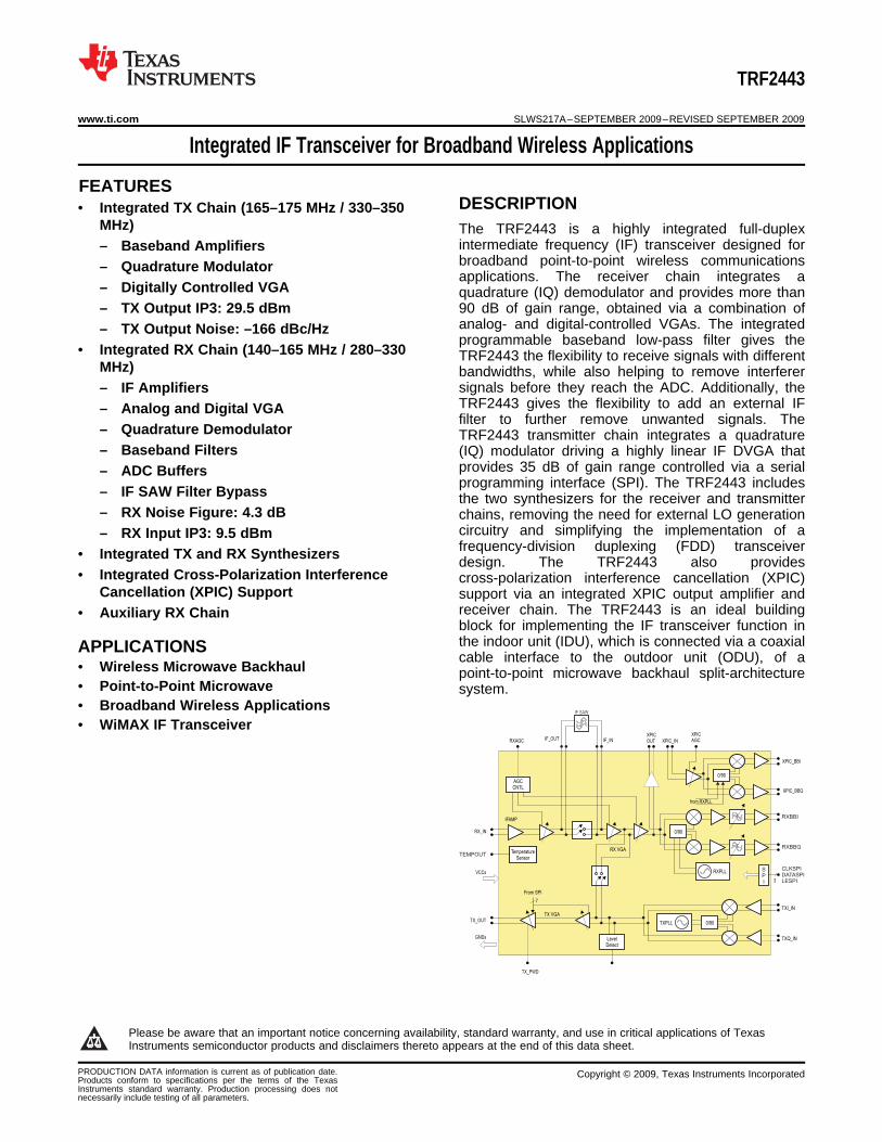
• Integrated TX Chain (165–175 MHz / 330–350MHz) The TRF2443 is a highly integrated full-duplex
intermediate frequency (IF) transceiver designed for– Baseband Amplifiersbroadband point-to-point wireless communications– Quadrature Modulatorapplications. The receiver chain integrates a
– Digitally Controlled VGA quadrature (IQ) demodulator and provides more than– TX Output IP3: 29.5 dBm 90 dB of gain range, obtained via a combination of
analog- and digital-controlled VGAs. The integrated– TX Output Noise: –166 dBc/Hzprogrammable baseband low-pass filter gives the
• Integrated RX Chain (140–165 MHz / 280–330 TRF2443 the flexibility to receive signals with differentMHz) bandwidths, while also helping to remove interferer
signals before they reach the ADC. Additionally, the– IF AmplifiersTRF2443 gives the flexibility to add an external IF– Analog and Digital VGAfilter to further remove unwanted signals. The
– Quadrature Demodulator TRF2443 transmitter chain integrates a quadrature– Baseband Filters (IQ) modulator driving a highly linear IF DVGA that
provides 35 dB of gain range controlled via a serial– ADC Buffersprogramming interface (SPI). The TRF2443 includes– IF SAW Filter Bypass the two synthesizers for the receiver and transmitter
– RX Noise Figure: 4.3 dB chains, removing the need for external LO generationcircuitry and simplifying the implementation of a– RX Input IP3: 9.5 dBmfrequency-division duplexing (FDD) transceiver• Integrated TX and RX Synthesizers design. The TRF2443 also provides
• Integrated Cross-Polarization Interference cross-polarization interference cancellation (XPIC)Cancellation (XPIC) Support support via an integrated XPIC output amplifier and
receiver chain. The TRF2443 is an ideal building• Auxiliary RX Chainblock for implementing the IF transceiver function inthe indoor unit (IDU), which is connected via a coaxialcable interface to the outdoor unit (ODU), of a
• Wireless Microwave Backhaul point-to-point microwave backhaul split-architecture• Point-to-Point Microwave system.• Broadband Wireless Applications• WiMAX IF Transceiver
1
Please be aware that an important notice concerning availability, standard warranty, and use in critical applications of TexasInstruments semiconductor products and disclaimers thereto appears at the end of this data sheet.
PRODUCTION DATA information is current as of publication date. Copyright © 2009, Texas Instruments IncorporatedProducts conform to specifications per the terms of the TexasInstruments standard warranty. Production processing does notnecessarily include testing of all parameters.
TRF2443 DEVICE DESCRIPTION
AGCCNTL
7
0/90TXPLL
3
RXAGC
VCCs
GNDs
RXPLL
TXQ_IN
TX_OUT
TXI_IN
RX_IN
RX VGA
TX VGA
IFAMP
From SPI
from RXPLL
XPIC_INXPICOUT
XPICAGC
XPIC_BBI
XPIC_BBQ
LevelDetect
IF SAW
IF_OUT IF_IN
TX_PWD
TemperatureSensor
CLKSPIDATASPILESPI
RXBBI
RXBBQ
TEMPOUT
0/90
0/90
SPI
RECEIVER DESCRIPTION
0/90
RX VGA
LNA
From SPI
from RXPLL
AGCCNTL
IFVGA1 IFVGA2 IFVGA3
From SPI
BB AMP/FLT
IF SAW
RX_IN
IF_OUT IF_IN
RX_BBI
RX_BBQ
RX_AGC
TRF2443
SLWS217A–SEPTEMBER 2009–REVISED SEPTEMBER 2009 ................................................................................................................................... www.ti.com
These devices have limited built-in ESD protection. The leads should be shorted together or the device placed in conductive foamduring storage or handling to prevent electrostatic damage to the MOS gates.
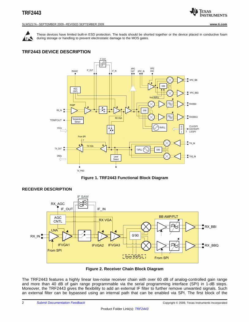
Figure 1. TRF2443 Functional Block Diagram
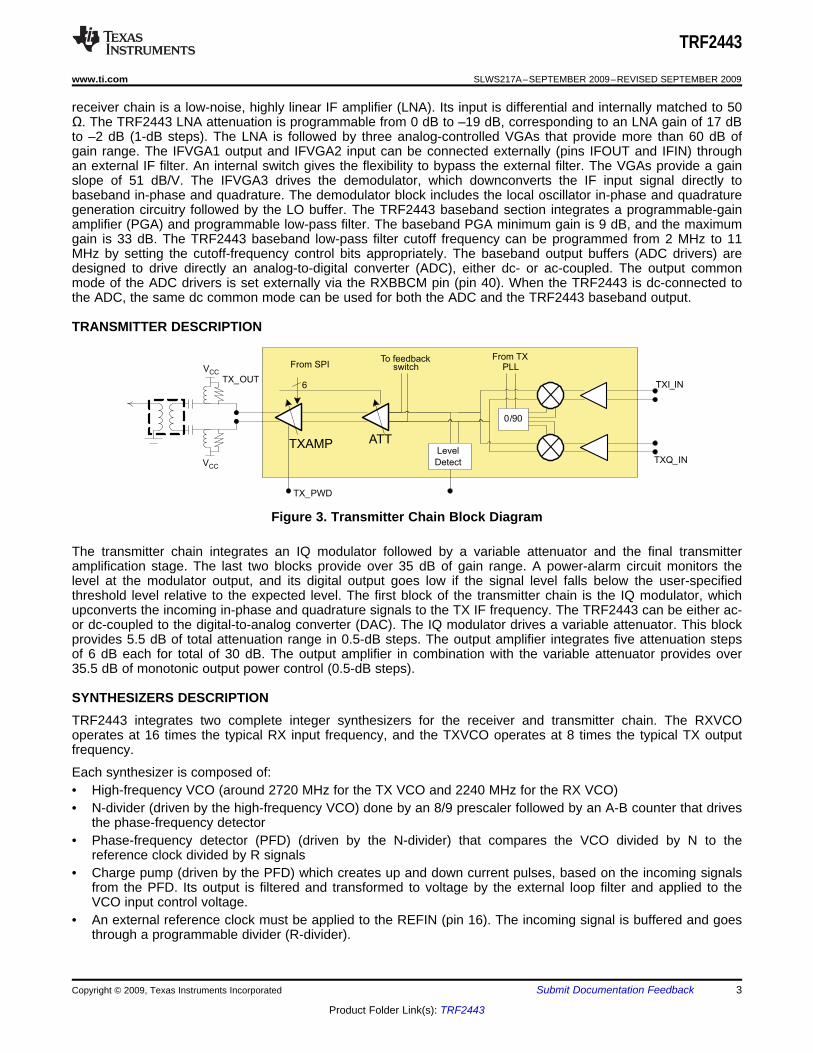
Figure 2. Receiver Chain Block Diagram
The TRF2443 features a highly linear low-noise receiver chain with over 60 dB of analog-controlled gain rangeand more than 40 dB of gain range programmable via the serial programming interface (SPI) in 1-dB steps.Moreover, the TRF2443 gives the flexibility to add an external IF filter to further remove unwanted signals. Suchan external filter can be bypassed using an internal path that can be enabled via SPI. The first block of the
2 Submit Documentation Feedback Copyright © 2009, Texas Instruments Incorporated
Product Folder Link(s): TRF2443
TRANSMITTER DESCRIPTION
6
From SPI
0/90
To feedbackswitch
From TXPLL
TX_OUT
TXQ_IN
TXI_IN
Level
Detect
TX_PWD
ATTTXAMP
VCC
VCC
SYNTHESIZERS DESCRIPTION
TRF2443
www.ti.com ................................................................................................................................... SLWS217A–SEPTEMBER 2009–REVISED SEPTEMBER 2009
receiver chain is a low-noise, highly linear IF amplifier (LNA). Its input is differential and internally matched to 50Ω. The TRF2443 LNA attenuation is programmable from 0 dB to –19 dB, corresponding to an LNA gain of 17 dBto –2 dB (1-dB steps). The LNA is followed by three analog-controlled VGAs that provide more than 60 dB ofgain range. The IFVGA1 output and IFVGA2 input can be connected externally (pins IFOUT and IFIN) throughan external IF filter. An internal switch gives the flexibility to bypass the external filter. The VGAs provide a gainslope of 51 dB/V. The IFVGA3 drives the demodulator, which downconverts the IF input signal directly tobaseband in-phase and quadrature. The demodulator block includes the local oscillator in-phase and quadraturegeneration circuitry followed by the LO buffer. The TRF2443 baseband section integrates a programmable-gainamplifier (PGA) and programmable low-pass filter. The baseband PGA minimum gain is 9 dB, and the maximumgain is 33 dB. The TRF2443 baseband low-pass filter cutoff frequency can be programmed from 2 MHz to 11MHz by setting the cutoff-frequency control bits appropriately. The baseband output buffers (ADC drivers) aredesigned to drive directly an analog-to-digital converter (ADC), either dc- or ac-coupled. The output commonmode of the ADC drivers is set externally via the RXBBCM pin (pin 40). When the TRF2443 is dc-connected tothe ADC, the same dc common mode can be used for both the ADC and the TRF2443 baseband output.
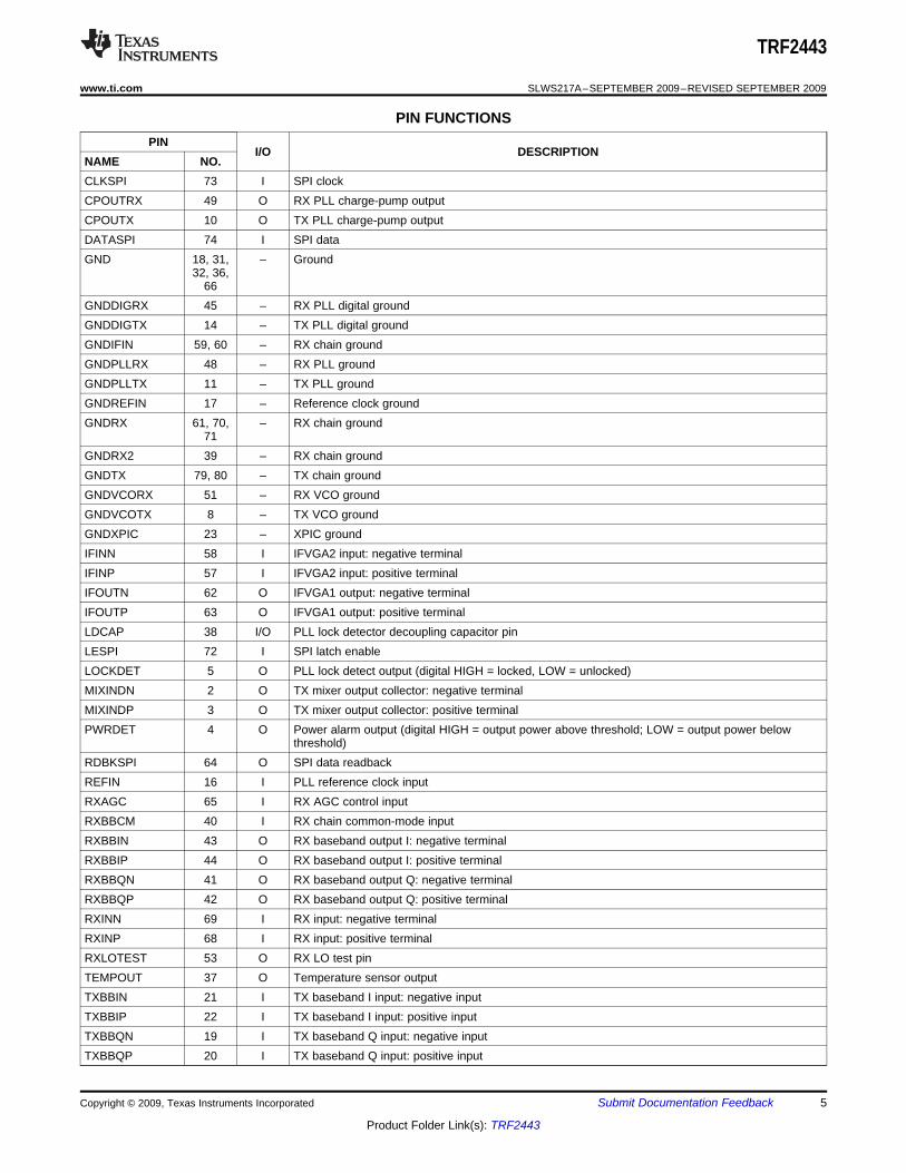
Figure 3. Transmitter Chain Block Diagram
The transmitter chain integrates an IQ modulator followed by a variable attenuator and the final transmitteramplification stage. The last two blocks provide over 35 dB of gain range. A power-alarm circuit monitors thelevel at the modulator output, and its digital output goes low if the signal level falls below the user-specifiedthreshold level relative to the expected level. The first block of the transmitter chain is the IQ modulator, whichupconverts the incoming in-phase and quadrature signals to the TX IF frequency. The TRF2443 can be either ac-or dc-coupled to the digital-to-analog converter (DAC). The IQ modulator drives a variable attenuator. This blockprovides 5.5 dB of total attenuation range in 0.5-dB steps. The output amplifier integrates five attenuation stepsof 6 dB each for total of 30 dB. The output amplifier in combination with the variable attenuator provides over35.5 dB of monotonic output power control (0.5-dB steps).
TRF2443 integrates two complete integer synthesizers for the receiver and transmitter chain. The RXVCOoperates at 16 times the typical RX input frequency, and the TXVCO operates at 8 times the typical TX outputfrequency.
Each synthesizer is composed of:• High-frequency VCO (around 2720 MHz for the TX VCO and 2240 MHz for the RX VCO)• N-divider (driven by the high-frequency VCO) done by an 8/9 prescaler followed by an A-B counter that drives
the phase-frequency detector• Phase-frequency detector (PFD) (driven by the N-divider) that compares the VCO divided by N to the
reference clock divided by R signals• Charge pump (driven by the PFD) which creates up and down current pulses, based on the incoming signals
from the PFD. Its output is filtered and transformed to voltage by the external loop filter and applied to theVCO input control voltage.
• An external reference clock must be applied to the REFIN (pin 16). The incoming signal is buffered and goesthrough a programmable divider (R-divider).
Copyright © 2009, Texas Instruments Incorporated Submit Documentation Feedback 3
Product Folder Link(s): TRF2443

XPIC DESCRIPTION
PINOUT DIAGRAM
22 23
GNDIFIN
TX
BB
IN
GNDIFIN
TX
BB
IP
IFINN
GN
DX
PIC
IFINP
XP
ICB
BC
M
VCCIFIN
XP
ICB
BQ
N
XPICOUTP
XP
ICB
BQ
P
XPICOUTN
XP
ICB
BIN
RXLOTEST
XP
ICB
BIP
VCCVCORX
VC
CX
PIC
GNDVCORX
XP
ICA
GC
VTUNERX
GN
D
CPOUTRX
GN
D
GNDPLLRX
VC
CX
PIC
2
VCCPLLRX
XP
ICIN
N
VCCDIGRX
XP
ICIN
P
GDNDIGRX
GN
D
RXBBIP
TE
MP
OU
T
RXBBIN
LD
CA
P
RXBBQP
GN
DR
X2
RXBBQN
RX
BB
CM
60
59
58
57
56
55
54
53
52
51
50
49
48
47
46
45
44
43
42
41
24
1
2
3
4
5
6
7
8
9
10
11
12
13
14
15
16
17
18
19
20
TXPWD
GN
DT
X
MIXINDN
GN
DT
X
MIXINDP
TX
OU
TN
PWRDET
TX
OU
TP
LOCKDET
VC
CT
X
TXLOTEST
VC
CS
PI
VCCVCOTX
DA
TA
SP
I
GNDVCOTX
CL
KS
PI
VTUNETX
LE
SP
I
CPOUTX
GN
DR
X
GNDPLLTX
GN
DR
X
VCCPLLTX
RX
INN
VCCDIGTX
RX
INP
GNDDIGTX
VC
CR
X
VCCREF
GN
D
REFIN
RX
AG
C
GNDREFIN
RD
BK
SP
I
GND
IFO
UT
P
TXBBQN
IFO
UT
N
TXBBQP
GN
DR
X
25 26 27 28
PFP Package(Top View)
79 78 77 76 7580 74 72 71 7073
29 30 31 32 33
69 68
21
67 66 65 64
34 35 36 37 38 39 40
63 62 61
TRF2443
P0027-04
TRF2443
SLWS217A–SEPTEMBER 2009–REVISED SEPTEMBER 2009 ................................................................................................................................... www.ti.com
The VCO output is then routed through a programmable divider by 8 or 16 to create the TX and RX LO signals.The TRF2443 features a lock-detect output pin (LOCKDET, pin 5). This is a digital output that is high when bothRX and TX synthesizers are locked, and it is low if one or both synthesizers are unlocked (or lose lock).
The TRF2443 provides cross-polarization interference cancellation (XPIC) support via an integrated XPIC outputamplifier and receiver chain. The XPIC output amplifier transmits the signal taken at the receiver demodulatorinput. The XPIC receiver section downconverts the input signal to baseband I and Q. It includes an IF VGAfollowed by a demodulator and a baseband amplifier.
4 Submit Documentation Feedback Copyright © 2009, Texas Instruments Incorporated
Product Folder Link(s): TRF2443
TRF2443
www.ti.com ................................................................................................................................... SLWS217A–SEPTEMBER 2009–REVISED SEPTEMBER 2009
PIN FUNCTIONSPIN
I/O DESCRIPTIONNAME NO.CLKSPI 73 I SPI clockCPOUTRX 49 O RX PLL charge-pump outputCPOUTX 10 O TX PLL charge-pump outputDATASPI 74 I SPI dataGND 18, 31, – Ground
32, 36,66
GNDDIGRX 45 – RX PLL digital groundGNDDIGTX 14 – TX PLL digital groundGNDIFIN 59, 60 – RX chain groundGNDPLLRX 48 – RX PLL groundGNDPLLTX 11 – TX PLL groundGNDREFIN 17 – Reference clock groundGNDRX 61, 70, – RX chain ground
71GNDRX2 39 – RX chain groundGNDTX 79, 80 – TX chain groundGNDVCORX 51 – RX VCO groundGNDVCOTX 8 – TX VCO groundGNDXPIC 23 – XPIC groundIFINN 58 I IFVGA2 input: negative terminalIFINP 57 I IFVGA2 input: positive terminalIFOUTN 62 O IFVGA1 output: negative terminalIFOUTP 63 O IFVGA1 output: positive terminalLDCAP 38 I/O PLL lock detector decoupling capacitor pinLESPI 72 I SPI latch enableLOCKDET 5 O PLL lock detect output (digital HIGH = locked, LOW = unlocked)MIXINDN 2 O TX mixer output collector: negative terminalMIXINDP 3 O TX mixer output collector: positive terminalPWRDET 4 O Power alarm output (digital HIGH = output power above threshold; LOW = output power below
threshold)RDBKSPI 64 O SPI data readbackREFIN 16 I PLL reference clock inputRXAGC 65 I RX AGC control inputRXBBCM 40 I RX chain common-mode inputRXBBIN 43 O RX baseband output I: negative terminalRXBBIP 44 O RX baseband output I: positive terminalRXBBQN 41 O RX baseband output Q: negative terminalRXBBQP 42 O RX baseband output Q: positive terminalRXINN 69 I RX input: negative terminalRXINP 68 I RX input: positive terminalRXLOTEST 53 O RX LO test pinTEMPOUT 37 O Temperature sensor outputTXBBIN 21 I TX baseband I input: negative inputTXBBIP 22 I TX baseband I input: positive inputTXBBQN 19 I TX baseband Q input: negative inputTXBBQP 20 I TX baseband Q input: positive input
Copyright © 2009, Texas Instruments Incorporated Submit Documentation Feedback 5
Product Folder Link(s): TRF2443
TRF2443
SLWS217A–SEPTEMBER 2009–REVISED SEPTEMBER 2009 ................................................................................................................................... www.ti.com
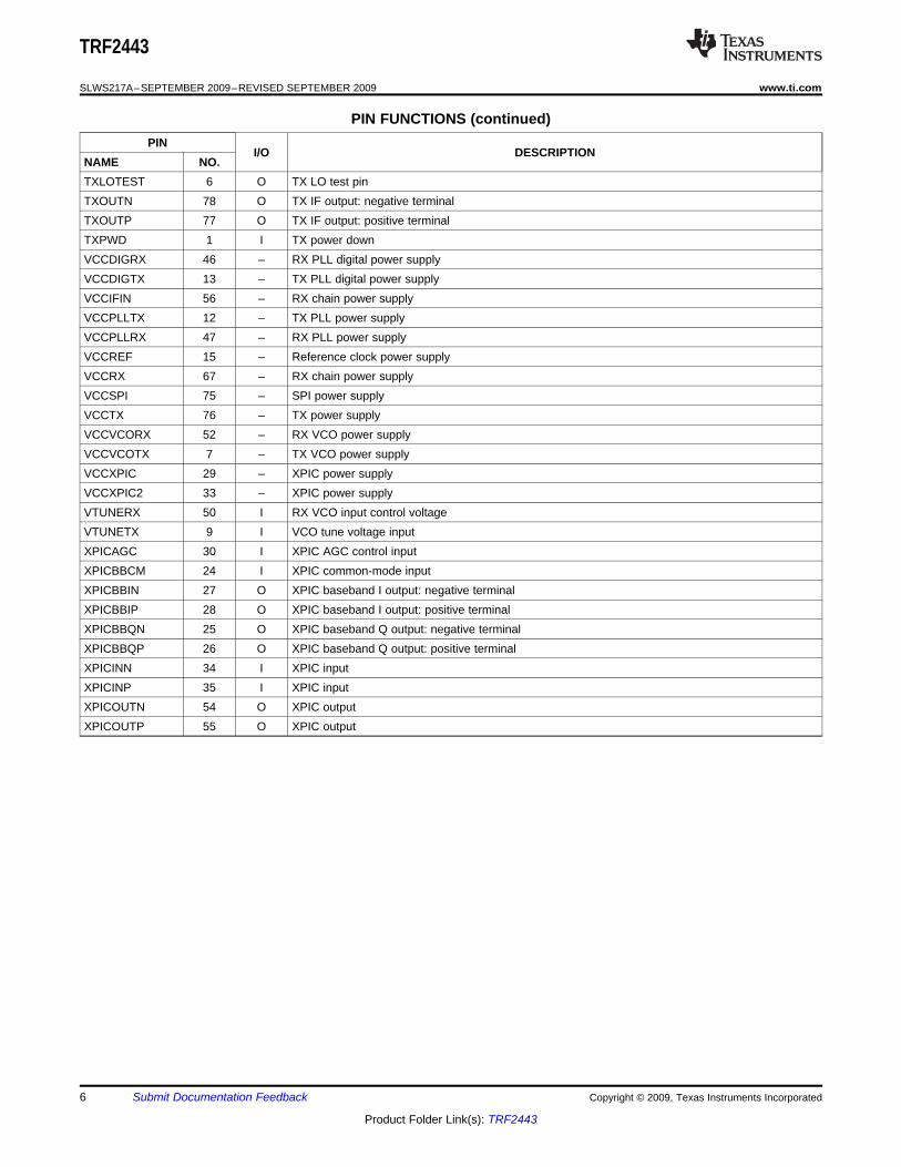
PIN FUNCTIONS (continued)PIN
I/O DESCRIPTIONNAME NO.TXLOTEST 6 O TX LO test pinTXOUTN 78 O TX IF output: negative terminalTXOUTP 77 O TX IF output: positive terminalTXPWD 1 I TX power downVCCDIGRX 46 – RX PLL digital power supplyVCCDIGTX 13 – TX PLL digital power supplyVCCIFIN 56 – RX chain power supplyVCCPLLTX 12 – TX PLL power supplyVCCPLLRX 47 – RX PLL power supplyVCCREF 15 – Reference clock power supplyVCCRX 67 – RX chain power supplyVCCSPI 75 – SPI power supplyVCCTX 76 – TX power supplyVCCVCORX 52 – RX VCO power supplyVCCVCOTX 7 – TX VCO power supplyVCCXPIC 29 – XPIC power supplyVCCXPIC2 33 – XPIC power supplyVTUNERX 50 I RX VCO input control voltageVTUNETX 9 I VCO tune voltage inputXPICAGC 30 I XPIC AGC control inputXPICBBCM 24 I XPIC common-mode inputXPICBBIN 27 O XPIC baseband I output: negative terminalXPICBBIP 28 O XPIC baseband I output: positive terminalXPICBBQN 25 O XPIC baseband Q output: negative terminalXPICBBQP 26 O XPIC baseband Q output: positive terminalXPICINN 34 I XPIC inputXPICINP 35 I XPIC inputXPICOUTN 54 O XPIC outputXPICOUTP 55 O XPIC output
6 Submit Documentation Feedback Copyright © 2009, Texas Instruments Incorporated
Product Folder Link(s): TRF2443

ABSOLUTE MAXIMUM RATINGS (1)
THERMAL CHARACTERISTICS
RECOMMENDED OPERATING CONDITIONS
DC CHARACTERISTICS
DIGITAL INTERFACE CHARACTERISTICS
TRF2443
www.ti.com ................................................................................................................................... SLWS217A–SEPTEMBER 2009–REVISED SEPTEMBER 2009
VALUE UNITInput voltage range (2) –0.3 to 5 VESD rating, HBM 2000 VESD rating, CDM 500 V
TJ Junction temperature range –40 to 150 °CTstg Storage temperature range –65 to 150 °C
(1) Stresses beyond those listed under absolute maximum ratings may cause permanent damage to the device. These are stress ratingsonly, and functional operation of the device at these or any other conditions beyond those indicated under recommended operatingconditions is not implied. Exposure to absolute-maximum-rated conditions for extended periods may affect device reliability.
(2) All voltage values are with respect to network ground terminal.
Over recommended operating free-air temperature (unless otherwise noted)
PARAMETER MIN TYP MAX UNITθJA Thermal derating, junction-to-ambient High-K board, still air 8.5 °C/W
Over operating free-air temperature range (unless otherwise noted)
MIN TYP MAX UNITVCC_3V 3.3-V power-supply voltage 3 3.3 3.6 VV_RXAGC Analog AGC voltage (pin 65) 0 2 VV_XPICAGC Analog AGC voltage (pin 30) 0 1 VTJ Operating junction temperature 0 65 125 °CTA Operating ambient temperature –40 85 °C
VCC = 3.3 V; TJ = 65°C
PARAMETER TEST CONDITIONS MIN TYP MAX UNITTX on; RX on (SAW off); XPIC off 947
ICC Total supply current TX on; RX on (SAW on); XPIC off 965 mATX on; RX on (SAW on); XPIC on 1085
VCC = 3.3 V; TJ = 65°C
PARAMETER TEST CONDITIONS MIN TYP MAX UNITVIH High-level input voltage 2 VCC VVIL Low-level input voltage 0 0.8 VVOH High-level output voltage 0.8 VCC VVOL Low-level output voltage 0.2 VCC V
Copyright © 2009, Texas Instruments Incorporated Submit Documentation Feedback 7
Product Folder Link(s): TRF2443
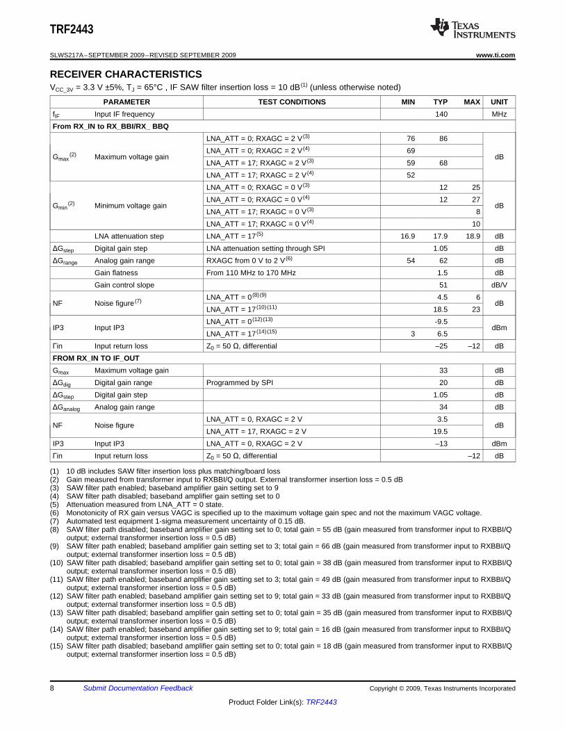
RECEIVER CHARACTERISTICS
TRF2443
SLWS217A–SEPTEMBER 2009–REVISED SEPTEMBER 2009 ................................................................................................................................... www.ti.com
VCC_3V = 3.3 V ±5%, TJ = 65°C , IF SAW filter insertion loss = 10 dB (1) (unless otherwise noted)
PARAMETER TEST CONDITIONS MIN TYP MAX UNITfIF Input IF frequency 140 MHzFrom RX_IN to RX_BBI/RX_ BBQ
LNA_ATT = 0; RXAGC = 2 V (3) 76 86LNA_ATT = 0; RXAGC = 2 V (4) 69
Gmax(2) Maximum voltage gain dB
LNA_ATT = 17; RXAGC = 2 V (3) 59 68LNA_ATT = 17; RXAGC = 2 V (4) 52LNA_ATT = 0; RXAGC = 0 V (3) 12 25LNA_ATT = 0; RXAGC = 0 V (4) 12 27
Gmin(2) Minimum voltage gain dB
LNA_ATT = 17; RXAGC = 0 V (3) 8LNA_ATT = 17; RXAGC = 0 V (4) 10
LNA attenuation step LNA_ATT = 17 (5) 16.9 17.9 18.9 dBΔGstep Digital gain step LNA attenuation setting through SPI 1.05 dBΔGrange Analog gain range RXAGC from 0 V to 2 V (6) 54 62 dB
Gain flatness From 110 MHz to 170 MHz 1.5 dBGain control slope 51 dB/V
LNA_ATT = 0 (8) (9) 4.5 6NF Noise figure (7) dB
LNA_ATT = 17 (10) (11) 18.5 23LNA_ATT = 0 (12) (13) -9.5
IP3 Input IP3 dBmLNA_ATT = 17 (14) (15) 3 6.5
Γin Input return loss Z0 = 50 Ω, differential –25 –12 dBFROM RX_IN TO IF_OUTGmax Maximum voltage gain 33 dBΔGdig Digital gain range Programmed by SPI 20 dBΔGstep Digital gain step 1.05 dBΔGanalog Analog gain range 34 dB
LNA_ATT = 0, RXAGC = 2 V 3.5NF Noise figure dB
LNA_ATT = 17, RXAGC = 2 V 19.5IP3 Input IP3 LNA_ATT = 0, RXAGC = 2 V –13 dBmΓin Input return loss Z0 = 50 Ω, differential –12 dB
(1) 10 dB includes SAW filter insertion loss plus matching/board loss(2) Gain measured from transformer input to RXBBI/Q output. External transformer insertion loss = 0.5 dB(3) SAW filter path enabled; baseband amplifier gain setting set to 9(4) SAW filter path disabled; baseband amplifier gain setting set to 0(5) Attenuation measured from LNA_ATT = 0 state.(6) Monotonicity of RX gain versus VAGC is specified up to the maximum voltage gain spec and not the maximum VAGC voltage.(7) Automated test equipment 1-sigma measurement uncertainty of 0.15 dB.(8) SAW filter path disabled; baseband amplifier gain setting set to 0; total gain = 55 dB (gain measured from transformer input to RXBBI/Q
output; external transformer insertion loss = 0.5 dB)(9) SAW filter path enabled; baseband amplifier gain setting set to 3; total gain = 66 dB (gain measured from transformer input to RXBBI/Q
output; external transformer insertion loss = 0.5 dB)(10) SAW filter path disabled; baseband amplifier gain setting set to 0; total gain = 38 dB (gain measured from transformer input to RXBBI/Q
output; external transformer insertion loss = 0.5 dB)(11) SAW filter path enabled; baseband amplifier gain setting set to 3; total gain = 49 dB (gain measured from transformer input to RXBBI/Q
output; external transformer insertion loss = 0.5 dB)(12) SAW filter path enabled; baseband amplifier gain setting set to 9; total gain = 33 dB (gain measured from transformer input to RXBBI/Q
output; external transformer insertion loss = 0.5 dB)(13) SAW filter path disabled; baseband amplifier gain setting set to 0; total gain = 35 dB (gain measured from transformer input to RXBBI/Q
output; external transformer insertion loss = 0.5 dB)(14) SAW filter path enabled; baseband amplifier gain setting set to 9; total gain = 16 dB (gain measured from transformer input to RXBBI/Q
output; external transformer insertion loss = 0.5 dB)(15) SAW filter path disabled; baseband amplifier gain setting set to 0; total gain = 18 dB (gain measured from transformer input to RXBBI/Q
output; external transformer insertion loss = 0.5 dB)
8 Submit Documentation Feedback Copyright © 2009, Texas Instruments Incorporated
Product Folder Link(s): TRF2443

TRF2443
www.ti.com ................................................................................................................................... SLWS217A–SEPTEMBER 2009–REVISED SEPTEMBER 2009
RECEIVER CHARACTERISTICS (continued)VCC_3V = 3.3 V ±5%, TJ = 65°C , IF SAW filter insertion loss = 10 dB (unless otherwise noted)
PARAMETER TEST CONDITIONS MIN TYP MAX UNITFROM IF_IN TO RX_BBI (OR RX_BBQ)Gmax Maximum voltage gain RXAGC = 2 V, RXBB_GAIN = 9 58 dBΔGdig Digital gain range Programmed by SPI 24 dBΔGstep Digital gain step 1 dBΔGanalog Analog gain range 28 dB
RXAGC = 2 V, RXBB_GAIN = 9 12.5NF Noise figure dB
RXAGC = 0 V, RXBB_GAIN = 9 28Image rejection See RX Image Rejection section -40 dBOutput common mode 1.5 V
Parallel capacitor 15 pFBaseband output load
Parallel resistor 1 kΩBASEBAND LOW-PASS FILTERfC_ON 3-dB cutoff frequency Filter on, programmed via SPI 2 11 MHzATT30M Filter rejection at 30 MHz Filter bypassed 1 dB
3-dB point with fC = 2.3 MHz (16) 2.2 MHz3-dB corner-frequency step (17) 25 kHzRejection at 4.5 MHz with fC = 2.3 MHz (16) 36Rejection at 8.75 MHz with fC = 2.3 MHz (16) 76 dB
Filter rejection Rejection at 17.5 MHz with fC = 2.3 MHz (16) 803-dB point with fC = 8.5 MHz (16) 8.3 MHzRejection at 18 MHz with fC = 8.5 MHz (16) 30Rejection at 35 MHz with fC = 8.5 MHz (16) 65 dBRejection at 70 MHz with fC = 8.5 MHz (16) 80
(16) After room-temperature cutoff-frequency calibration(17) Baseband filter 3-dB corner frequency control step via SPI around fC = 2.3 MHz
Copyright © 2009, Texas Instruments Incorporated Submit Documentation Feedback 9
Product Folder Link(s): TRF2443
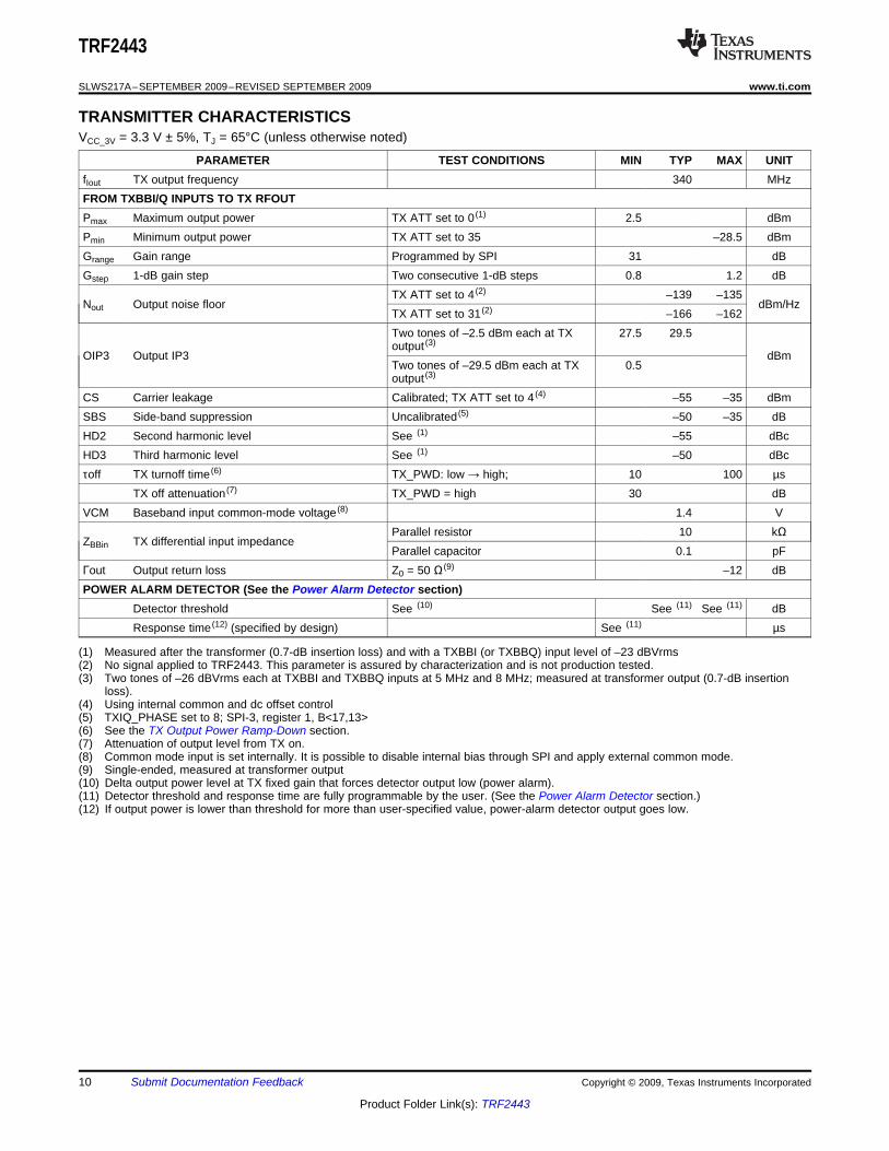
TRANSMITTER CHARACTERISTICS
TRF2443
SLWS217A–SEPTEMBER 2009–REVISED SEPTEMBER 2009 ................................................................................................................................... www.ti.com
VCC_3V = 3.3 V ± 5%, TJ = 65°C (unless otherwise noted)
PARAMETER TEST CONDITIONS MIN TYP MAX UNITfIout TX output frequency 340 MHzFROM TXBBI/Q INPUTS TO TX RFOUTPmax Maximum output power TX ATT set to 0 (1) 2.5 dBmPmin Minimum output power TX ATT set to 35 –28.5 dBmGrange Gain range Programmed by SPI 31 dBGstep 1-dB gain step Two consecutive 1-dB steps 0.8 1.2 dB
TX ATT set to 4 (2) –139 –135Nout Output noise floor dBm/Hz
TX ATT set to 31 (2) –166 –162Two tones of –2.5 dBm each at TX 27.5 29.5output (3)
OIP3 Output IP3 dBmTwo tones of –29.5 dBm each at TX 0.5output (3)
CS Carrier leakage Calibrated; TX ATT set to 4 (4) –55 –35 dBmSBS Side-band suppression Uncalibrated (5) –50 –35 dBHD2 Second harmonic level See (1) –55 dBcHD3 Third harmonic level See (1) –50 dBcτoff TX turnoff time (6) TX_PWD: low → high; 10 100 µs
TX off attenuation (7) TX_PWD = high 30 dBVCM Baseband input common-mode voltage (8) 1.4 V
Parallel resistor 10 kΩZBBin TX differential input impedance
Parallel capacitor 0.1 pFΓout Output return loss Z0 = 50 Ω (9) –12 dBPOWER ALARM DETECTOR (See the Power Alarm Detector section)
Detector threshold See (10) See (11) See (11) dBResponse time (12) (specified by design) See (11) µs
(1) Measured after the transformer (0.7-dB insertion loss) and with a TXBBI (or TXBBQ) input level of –23 dBVrms(2) No signal applied to TRF2443. This parameter is assured by characterization and is not production tested.(3) Two tones of –26 dBVrms each at TXBBI and TXBBQ inputs at 5 MHz and 8 MHz; measured at transformer output (0.7-dB insertion
loss).(4) Using internal common and dc offset control(5) TXIQ_PHASE set to 8; SPI-3, register 1, B<17,13>(6) See the TX Output Power Ramp-Down section.(7) Attenuation of output level from TX on.(8) Common mode input is set internally. It is possible to disable internal bias through SPI and apply external common mode.(9) Single-ended, measured at transformer output(10) Delta output power level at TX fixed gain that forces detector output low (power alarm).(11) Detector threshold and response time are fully programmable by the user. (See the Power Alarm Detector section.)(12) If output power is lower than threshold for more than user-specified value, power-alarm detector output goes low.
10 Submit Documentation Feedback Copyright © 2009, Texas Instruments Incorporated
Product Folder Link(s): TRF2443

RF SYNTHESIZER CHARACTERISTICS
TRF2443
www.ti.com ................................................................................................................................... SLWS217A–SEPTEMBER 2009–REVISED SEPTEMBER 2009
VCC_3V = 3.3 V ±5%, TJ = 65°C (unless otherwise noted)
PARAMETER TEST CONDITIONS MIN TYP MAX UNITTXVCOftxvco TXVCO frequency range See (1) 2640 2800 MHz
Divide-by-8 mode 330 350ftxlo TXLO frequency range MHz
Divide-by-16 mode 165 175fout = 340 MHz; offset = 10 kHz –92.5fout = 340 MHz; offset = 100 kHz –117.5
TXLO free-running phase noise dBc/Hzfout = 340 MHz; offset = 1 MHz –140fout = 340 MHz; offset = 20 MHz –150
KvTX TXVCO gain 45 MHz/VTXPLLfPFD PFD frequency 20 MHz
fout = 340 MHz; offset = 20 kHz –117fout = 340 MHz; offset = 100 kHz –116
TXLO closed-loop phase noise dBc/Hzfout = 340 MHz; offset = 1 MHz –140fout = 340 MHz; offset = 20 MHz –150
Integrated TXLO noise Integrated from 1 kHz to 12 MHz; fout = 340 MHz (2) –56.5 dBReference spur Measured at TXLOTEST (2720 MHz) –70 dBc
From unlocked state to locked state (includesLock time 300 µsdigital-calibration time) (3)
fout = 165 MHz; offset = 20 kHz –121fout = 165 MHz; offset = 100 kHz –120
TXLO closed-loop phase noise dBc/Hzfout = 165 MHz; offset = 1 MHz –141fout = 165 MHz; offset = 20 MHz –147
Vccmin PLL-lock minimum power supply TJ = 65°C 2.8 VRXVCOfrxvco RXVCO frequency range See (1) 2240 2640 MHz
Divide-by-8 mode 280 330frxlo RXLO frequency range MHz
Divide-by-16 mode 140 165fout = 140 MHz; offset = 10 kHz –97.5fout = 140 MHz; offset = 100 kHz –122.5
RXLO free-running phase noise dBc/Hzfout = 140 MHz; offset = 1 MHz –146fout = 140 MHz; offset = 20 MHz –150
KvRX RXVCO gain 45 MHz/VRXPLLfPFD PFD frequency 20 MHz
Integrated from 1 kHz to 12 MHz; fout = 140 MHz (2) –62Integrated RXLO noise dB
Integrated from 1 kHz to 12 MHz; fout = 160 MHz (2) –60fout = 140 MHz; offset = 20 kHz –122fout = 140 MHz; offset = 100 kHz –121
RXLO closed-loop phase noise dBc/Hzfout = 140 MHz; offset = 1 MHz –146fout = 140 MHz; offset = 20 MHz –150
Reference spur Measured at RXLOTEST (2240 MHz) –65 dBcFrom unlock state to lock state (includesLock time 300 µsdigital-calibration time) (3)
(1) Frequency range proven locked with PFD frequency = 20 MHz(2) Optimized for lowest integrated noise; see the Reference-Clock Characteristics table for recommended reference clock performance.(3) Charge-pump current = 1 mA, PFD frequency = 20 MHz, loop filter optimized (see Application Schematic section)
Copyright © 2009, Texas Instruments Incorporated Submit Documentation Feedback 11
Product Folder Link(s): TRF2443
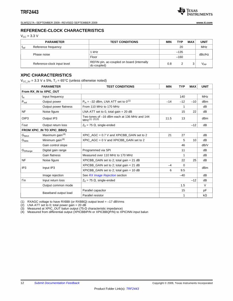
REFERENCE-CLOCK CHARACTERISTICS
XPIC CHARACTERISTICS
TRF2443
SLWS217A–SEPTEMBER 2009–REVISED SEPTEMBER 2009 ................................................................................................................................... www.ti.com
VCC = 3.3 V
PARAMETER TEST CONDITIONS MIN TYP MAX UNITfref Reference frequency 20 MHz
1 kHz –135Phase noise dBc/Hz
Floor –160REFIN pin, ac-coupled on board (internallyReference-clock input level 0.8 2 3 VPPdc-coupled)
VCC_3V = 3.3 V ± 5%, TJ = 65°C (unless otherwise noted)
PARAMETER TEST CONDITIONS MIN TYP MAX UNITFrom RX_IN to XPIC_OUTfin Input frequency 140 MHzPout Output power Pin = –32 dBm, LNA ATT set to 0 (1) –14 –12 –10 dBm
Output power flatness From 110 MHz to 170 MHz 1 dBNF Noise figure LNA ATT set to 0, total gain = 20 dB 15 22 dB
Two tones of –16 dBm each at 136 MHz and 144OIP3 Output IP3 11.5 13 dBmMHz (1) (2) (3)
Γout Output return loss Z0 = 75 Ω, single-ended –12 dBFROM XPIC_IN TO XPIC_BBI/QGMAX Maximum gain (4) XPIC_AGC = 0.7 V and XPICBB_GAIN set to 2 21 27 dBGMIN Minimum gain (4) XPIC_AGC = 0 V and XPICBB_GAIN set to 2 5 10 dB
Gain control slope 46 dB/VGDRange Digital gain range Programmed via SPI 11 dB
Gain flatness Measured over 110 MHz to 170 MHz 1 dBNF Noise figure XPICBB_GAIN set to 2; total gain = 21 dB 22 25 dB
XPICBB_GAIN set to 2; total gain = 21 dB –4 0IP3 Input IP3 dBm
XPICBB_GAIN set to 2; total gain = 10 dB 6 9.5Image rejection See RX Image Rejection section –40 dB
Γin Input return loss Z0 = 75 Ω, single-ended –12 dBOutput common mode 1.5 V
Parallel capacitor 15 pFBaseband output load
Parallel resistor 1 kΩ
(1) RXAGC voltage to have RXBBI (or RXBBQ) output level = –17 dBVrms(2) LNA ATT set to 0; total power gain = 20 dB(3) Measured at XPIC_OUT balun output (75-Ω characteristic impedance)(4) Measured from differential output (XPICBBIP/N or XPICBBQP/N) to XPICINN input balun
12 Submit Documentation Feedback Copyright © 2009, Texas Instruments Incorporated
Product Folder Link(s): TRF2443

RECEIVER TYPICAL CHARACTERISTICS
RX AGC Voltage (mV)
0
10
20
30
40
50
60
70
80
90
0 200 400 600 800 1000 1200 1400 1600 1800
RX
Gai
n (d
B)
G001
TJ = 0°CTJ = 65°CTJ = 125°C
0
10
20
30
40
50
60
70
80
90
0 200 400 600 800 1000 1200 1400 1600 1800
RX
Gai
n (d
B)
VCC = 3.1VVCC = 3.3VVCC = 3.5V
RX AGC Voltage (mV)G002
−90
−80
−70
−60
−50
−40
−30
−20
−10
0
10
0 10 20 30 40 50 60 70 80 90
RX
Inpu
t IP
3 (d
Bm
)
TJ = 0°CTJ = 65°CTJ = 125°C
RX Gain (dB)G003
−90
−80
−70
−60
−50
−40
−30
−20
−10
0
10
0 10 20 30 40 50 60 70 80 90
RX
Inpu
t IP
3 (d
Bm
)
VCC = 3.1VVCC = 3.3VVCC = 3.5V
RX Gain (dB)G004
0
5
10
15
20
25
30
35
40
45
50
0 10 20 30 40 50 60 70 80 90
RX
Noi
se F
igur
e (d
B)
TJ = 0°CTJ = 65°CTJ = 125°C
RX Gain (dB)G005
0
5
10
15
20
25
30
35
40
45
50
0 10 20 30 40 50 60 70 80 90
RX
Noi
se F
igur
e (d
B)
VCC = 3.1VVCC = 3.3VVCC = 3.5V
RX Gain (dB)G006
TRF2443
www.ti.com ................................................................................................................................... SLWS217A–SEPTEMBER 2009–REVISED SEPTEMBER 2009
fin= 140 MHz, SAW_EN = 0, LNA_ATT = 0, baseband gain setting = 0, 3-dB pad enabled (TJ = 65°C, VCC = 3.3 V, unlessotherwise noted)
RX GAIN RX GAINvs vs
RX AGC VOLTAGE RX AGC VOLTAGE
Figure 4. Figure 5.
RX INPUT IP3 RX INPUT IP3vs vs
RX GAIN RX GAIN
Figure 6. Figure 7.
RX NOISE FIGURE RX NOISE FIGUREvs vs
RX GAIN RX GAIN
Figure 8. Figure 9.
Copyright © 2009, Texas Instruments Incorporated Submit Documentation Feedback 13
Product Folder Link(s): TRF2443
RECEIVER TYPICAL CHARACTERISTICS
0
10
20
30
40
50
60
70
80
90
0 200 400 600 800 1000 1200 1400 1600 1800
RX
Gai
n (d
B)
TJ = 0°CTJ = 65°CTJ = 125°C
RX AGC Voltage (mV)G007
0
10
20
30
40
50
60
70
80
90
0 200 400 600 800 1000 1200 1400 1600 1800
RX
Gai
n (d
B)
VCC = 3.1VVCC = 3.3VVCC = 3.5V
RX AGC Voltage (mV)G008
−90
−80
−70
−60
−50
−40
−30
−20
−10
0
10
0 10 20 30 40 50 60 70 80 90
RX
Inpu
t IP
3 (d
Bm
)
TJ = 0°CTJ = 65°CTJ = 125°C
RX Gain (dB)G009
−90
−80
−70
−60
−50
−40
−30
−20
−10
0
10
0 10 20 30 40 50 60 70 80 90
RX
Inpu
t IP
3 (d
Bm
)
VCC = 3.1VVCC = 3.3VVCC = 3.5V
RX Gain (dB)G010
0
5
10
15
20
25
30
35
40
45
50
0 10 20 30 40 50 60 70 80 90
RX
Noi
se F
igur
e (d
B)
TJ = 0°CTJ = 65°CTJ = 125°C
RX Gain (dB)G011
0
5
10
15
20
25
30
35
40
45
50
0 10 20 30 40 50 60 70 80 90
RX
Noi
se F
igur
e (d
B)
VCC = 3.1VVCC = 3.3VVCC = 3.5V
RX Gain (dB)G012
TRF2443
SLWS217A–SEPTEMBER 2009–REVISED SEPTEMBER 2009 ................................................................................................................................... www.ti.com
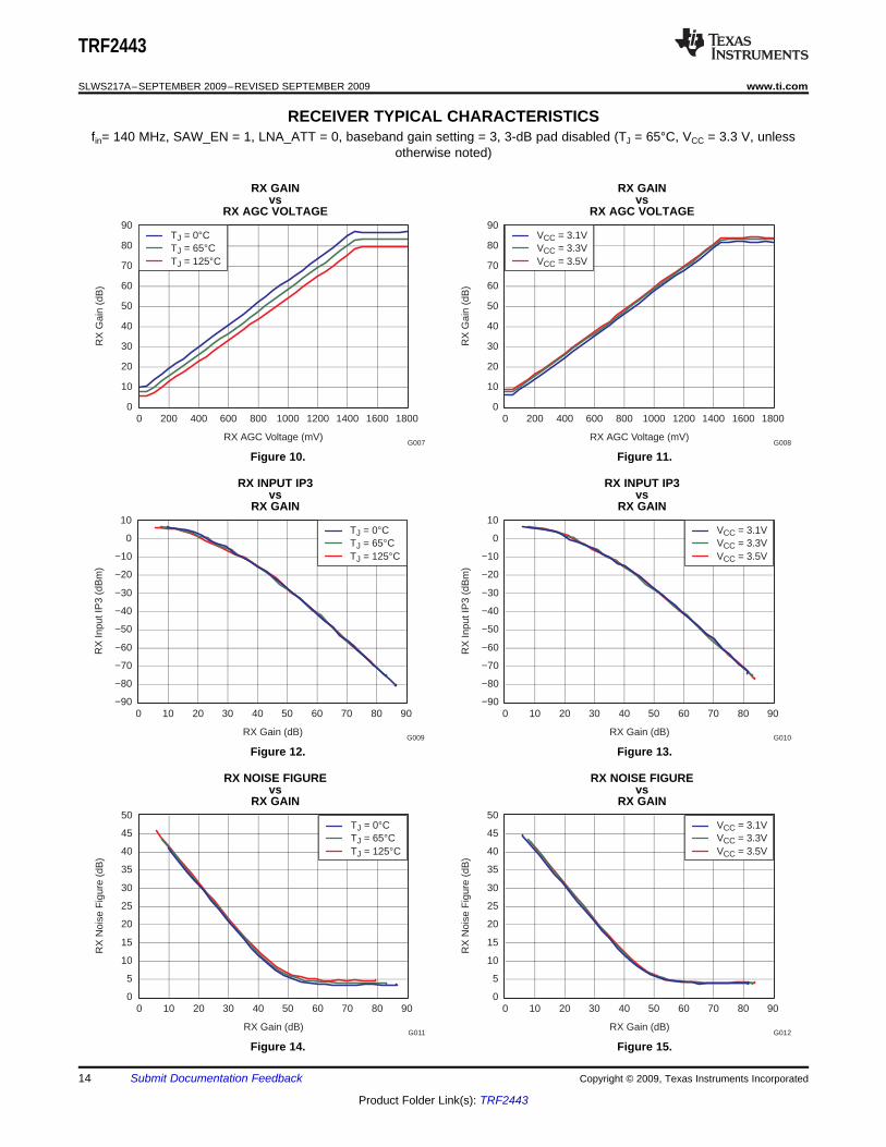
fin= 140 MHz, SAW_EN = 1, LNA_ATT = 0, baseband gain setting = 3, 3-dB pad disabled (TJ = 65°C, VCC = 3.3 V, unlessotherwise noted)
RX GAIN RX GAINvs vs
RX AGC VOLTAGE RX AGC VOLTAGE
Figure 10. Figure 11.
RX INPUT IP3 RX INPUT IP3vs vs
RX GAIN RX GAIN
Figure 12. Figure 13.
RX NOISE FIGURE RX NOISE FIGUREvs vs
RX GAIN RX GAIN
Figure 14. Figure 15.
14 Submit Documentation Feedback Copyright © 2009, Texas Instruments Incorporated
Product Folder Link(s): TRF2443

RECEIVER TYPICAL CHARACTERISTICS
0
10
20
30
40
50
60
70
80
90
100
0 200 400 600 800 1000 1200 1400 1600 1800
RX
Gai
n (d
B)
TJ = 0°CTJ = 65°CTJ = 125°C
RX AGC Voltage (mV)G013
0
10
20
30
40
50
60
70
80
90
100
0 200 400 600 800 1000 1200 1400 1600 1800
RX
Gai
n (d
B)
VCC = 3.1VVCC = 3.3VVCC = 3.5V
RX AGC Voltage (mV)G014
−90
−80
−70
−60
−50
−40
−30
−20
−10
0
10
0 10 20 30 40 50 60 70 80 90
RX
Inpu
t IP
3 (d
Bm
)
TJ = 0°CTJ = 65°CTJ = 125°C
RX Gain (dB)G015
−90
−80
−70
−60
−50
−40
−30
−20
−10
0
10
0 10 20 30 40 50 60 70 80 90
RX
Inpu
t IP
3 (d
Bm
)
VCC = 3.1VVCC = 3.3VVCC = 3.5V
RX Gain (dB)G016
0
5
10
15
20
25
30
35
40
45
50
0 10 20 30 40 50 60 70 80 90
RX
Noi
se F
igur
e (d
B)
TJ = 0°CTJ = 65°CTJ = 125°C
RX Gain (dB)G017
0
5
10
15
20
25
30
35
40
45
50
0 10 20 30 40 50 60 70 80 90
RX
Noi
se F
igur
e (d
B)
VCC = 3.1VVCC = 3.3VVCC = 3.5V
RX Gain (dB)G018
TRF2443
www.ti.com ................................................................................................................................... SLWS217A–SEPTEMBER 2009–REVISED SEPTEMBER 2009
fin= 140 MHz, SAW_EN = 1, LNA_ATT = 0, baseband gain setting = 6, 3-dB pad disabled (TJ = 65°C, VCC = 3.3 V, unlessotherwise noted)
RX GAIN RX GAINvs vs
RX AGC VOLTAGE RX AGC VOLTAGE
Figure 16. Figure 17.
RX INPUT IP3 RX INPUT IP3vs vs
RX GAIN RX GAIN
Figure 18. Figure 19.
RX NOISE FIGURE RX NOISE FIGUREvs vs
RX GAIN RX GAIN
Figure 20. Figure 21.
Copyright © 2009, Texas Instruments Incorporated Submit Documentation Feedback 15
Product Folder Link(s): TRF2443
RECEIVER TYPICAL CHARACTERISTICS
0
10
20
30
40
50
60
70
80
90
100
0 200 400 600 800 1000 1200 1400 1600 1800
RX
Gai
n (d
B)
TJ = 0°CTJ = 65°CTJ = 125°C
RX AGC Voltage (mV)G019
0
10
20
30
40
50
60
70
80
90
100
0 200 400 600 800 1000 1200 1400 1600 1800
RX
Gai
n (d
B)
VCC = 3.1VVCC = 3.3VVCC = 3.5V
RX AGC Voltage (mV)G020
−90
−80
−70
−60
−50
−40
−30
−20
−10
0
10
0 10 20 30 40 50 60 70 80 90 100
RX
Inpu
t IP
3 (d
Bm
)
TJ = 0°CTJ = 65°CTJ = 125°C
RX Gain (dB)G021
−90
−80
−70
−60
−50
−40
−30
−20
−10
0
10
0 10 20 30 40 50 60 70 80 90 100
RX
Inpu
t IP
3 (d
Bm
)
VCC = 3.1VVCC = 3.3VVCC = 3.5V
RX Gain (dB)G022
0
5
10
15
20
25
30
35
40
45
50
0 10 20 30 40 50 60 70 80 90 100
RX
Noi
se F
igur
e (d
B)
TJ = 0°CTJ = 65°CTJ = 125°C
RX Gain (dB)G023
0
5
10
15
20
25
30
35
40
45
50
0 10 20 30 40 50 60 70 80 90 100
RX
Noi
se F
igur
e (d
B)
VCC = 3.1VVCC = 3.3VVCC = 3.5V
RX Gain (dB)G024
TRF2443
SLWS217A–SEPTEMBER 2009–REVISED SEPTEMBER 2009 ................................................................................................................................... www.ti.com
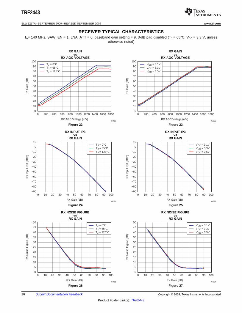
fin= 140 MHz, SAW_EN = 1, LNA_ATT = 0, baseband gain setting = 9, 3-dB pad disabled (TJ = 65°C, VCC = 3.3 V, unlessotherwise noted)
RX GAIN RX GAINvs vs
RX AGC VOLTAGE RX AGC VOLTAGE
Figure 22. Figure 23.
RX INPUT IP3 RX INPUT IP3vs vs
RX GAIN RX GAIN
Figure 24. Figure 25.
RX NOISE FIGURE RX NOISE FIGUREvs vs
RX GAIN RX GAIN
Figure 26. Figure 27.
16 Submit Documentation Feedback Copyright © 2009, Texas Instruments Incorporated
Product Folder Link(s): TRF2443
RECEIVER TYPICAL CHARACTERISTICS
LNA Attenuation Setting (SPI-3, REG2<9,6>)
−20
−18
−16
−14
−12
−10
−8
−6
−4
−2
0
0 2 4 6 8 10 12 14 16 18 20
RX
LN
A A
ttenu
atio
n (d
B)
G037
TJ = 0°CTJ = 65°CTJ = 125°C
−20
−18
−16
−14
−12
−10
−8
−6
−4
−2
0
0 2 4 6 8 10 12 14 16 18 20
RX
LN
A A
ttenu
atio
n (d
B)
VCC = 3.1VVCC = 3.3VVCC = 3.5V
LNA Attenuation Setting (SPI-3, REG2<9,6>)G038
−2.0
−1.5
−1.0
−0.5
0.0
0.5
1.0
1.5
2.0
0 1 2 3 4 5 6 7 8 9 10 11 12 13 14 15 16 17 18 19
RX
LN
A C
umul
ativ
e A
ttenu
atio
n E
rror
(dB
)
TJ = 0°CTJ = 65°CTJ = 125°C
LNA Attenuation Setting (SPI-3, REG2<9,6>)G086
−2.0
−1.5
−1.0
−0.5
0.0
0.5
1.0
1.5
2.0
0 1 2 3 4 5 6 7 8 9 10 11 12 13 14 15 16 17 18 19
RX
LN
A C
umul
ativ
e A
ttenu
atio
n E
rror
(dB
)
VCC = 3.1VVCC = 3.3VVCC = 3.5V
LNA Attenuation Setting (SPI-3, REG2<9,6>)G087
RXBB Gain Setting (SPI-3, REG2<15,11>)
8
10
12
14
16
18
20
22
24
26
28
30
32
0 2 4 6 8 10 12 14 16 18 20 22 24
RX
Bas
eban
d G
ain
(dB
)
G039
TJ = 0°CTJ = 65°CTJ = 125°C
8
10
12
14
16
18
20
22
24
26
28
30
32
0 2 4 6 8 10 12 14 16 18 20 22 24
RX
Bas
eban
d G
ain
(dB
)
VCC = 3.1VVCC = 3.3VVCC = 3.5V
RXBB Gain Setting (SPI-3, REG2<15,11>)G040
TRF2443
www.ti.com ................................................................................................................................... SLWS217A–SEPTEMBER 2009–REVISED SEPTEMBER 2009
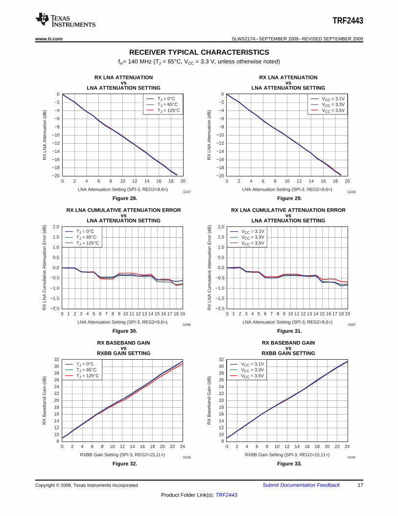
fin= 140 MHz (TJ = 65°C, VCC = 3.3 V, unless otherwise noted)
RX LNA ATTENUATION RX LNA ATTENUATIONvs vs
LNA ATTENUATION SETTING LNA ATTENUATION SETTING
Figure 28. Figure 29.
RX LNA CUMULATIVE ATTENUATION ERROR RX LNA CUMULATIVE ATTENUATION ERRORvs vs
LNA ATTENUATION SETTING LNA ATTENUATION SETTING
Figure 30. Figure 31.
RX BASEBAND GAIN RX BASEBAND GAINvs vs
RXBB GAIN SETTING RXBB GAIN SETTING
Figure 32. Figure 33.
Copyright © 2009, Texas Instruments Incorporated Submit Documentation Feedback 17
Product Folder Link(s): TRF2443
−3.0
−2.5
−2.0
−1.5
−1.0
−0.5
0.0
0.5
1.0
1.5
2.0
2.5
3.0
0 2 4 6 8 10 12 14 16 18 20 22 24
RX
Bas
eban
d C
umul
ativ
e G
ain
Err
or (
dB)
TJ = 0°CTJ = 65°CTJ = 125°C
RXBB Gain Setting (SPI-3, REG2<15,11>)G088
−3.0
−2.5
−2.0
−1.5
−1.0
−0.5
0.0
0.5
1.0
1.5
2.0
2.5
3.0
0 2 4 6 8 10 12 14 16 18 20 22 24
RX
Bas
eban
d C
umul
ativ
e G
ain
Err
or (
dB)
VCC = 3.1VVCC = 3.3VVCC = 3.5V
RXBB Gain Setting (SPI-3, REG2<15,11>)G089
TRF2443
SLWS217A–SEPTEMBER 2009–REVISED SEPTEMBER 2009 ................................................................................................................................... www.ti.com
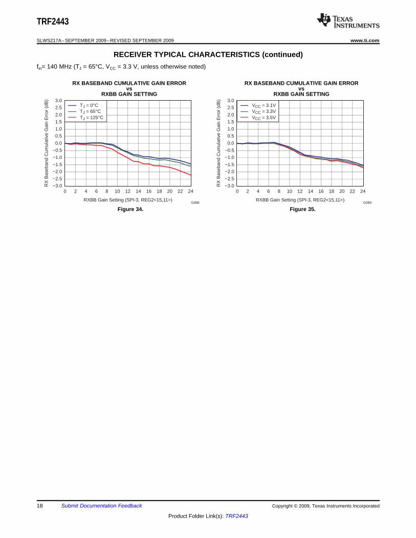
RECEIVER TYPICAL CHARACTERISTICS (continued)fin= 140 MHz (TJ = 65°C, VCC = 3.3 V, unless otherwise noted)
RX BASEBAND CUMULATIVE GAIN ERROR RX BASEBAND CUMULATIVE GAIN ERRORvs vs
RXBB GAIN SETTING RXBB GAIN SETTING
Figure 34. Figure 35.
18 Submit Documentation Feedback Copyright © 2009, Texas Instruments Incorporated
Product Folder Link(s): TRF2443
RECEIVER TYPICAL CHARACTERISTICS
0
10
20
30
40
50
60
70
80
90
0 200 400 600 800 1000 1200 1400 1600 1800
RX
BB
I Gai
n (d
B)
TJ = 0°CTJ = 65°CTJ = 125°C
RX AGC Voltage (mV)G074
0
10
20
30
40
50
60
70
80
90
0 200 400 600 800 1000 1200 1400 1600 1800
RX
BB
I Gai
n (d
B)
VCC = 3.1VVCC = 3.3VVCC = 3.5V
RX AGC Voltage (mV)G075
−80
−70
−60
−50
−40
−30
−20
−10
0
10
20
0 10 20 30 40 50 60 70 80 90
RX
BB
I Inp
ut IP
3 (d
Bm
)
TJ = 0°CTJ = 65°CTJ = 125°C
RX Gain (dB)G076
−80
−70
−60
−50
−40
−30
−20
−10
0
10
20
0 10 20 30 40 50 60 70 80 90
RX
BB
I Inp
ut IP
3 (d
Bm
)
VCC = 3.1VVCC = 3.3VVCC = 3.5V
RX Gain (dB)G077
0
5
10
15
20
25
30
35
40
45
50
0 10 20 30 40 50 60 70 80 90
RX
BB
I Noi
se F
igur
e (d
B)
TJ = 0°CTJ = 65°CTJ = 125°C
RX Gain (dB)G078
0
5
10
15
20
25
30
35
40
45
50
0 10 20 30 40 50 60 70 80 90
RX
BB
I Noi
se F
igur
e (d
B)
VCC = 3.1VVCC = 3.3VVCC = 3.5V
RX Gain (dB)G079
TRF2443
www.ti.com ................................................................................................................................... SLWS217A–SEPTEMBER 2009–REVISED SEPTEMBER 2009
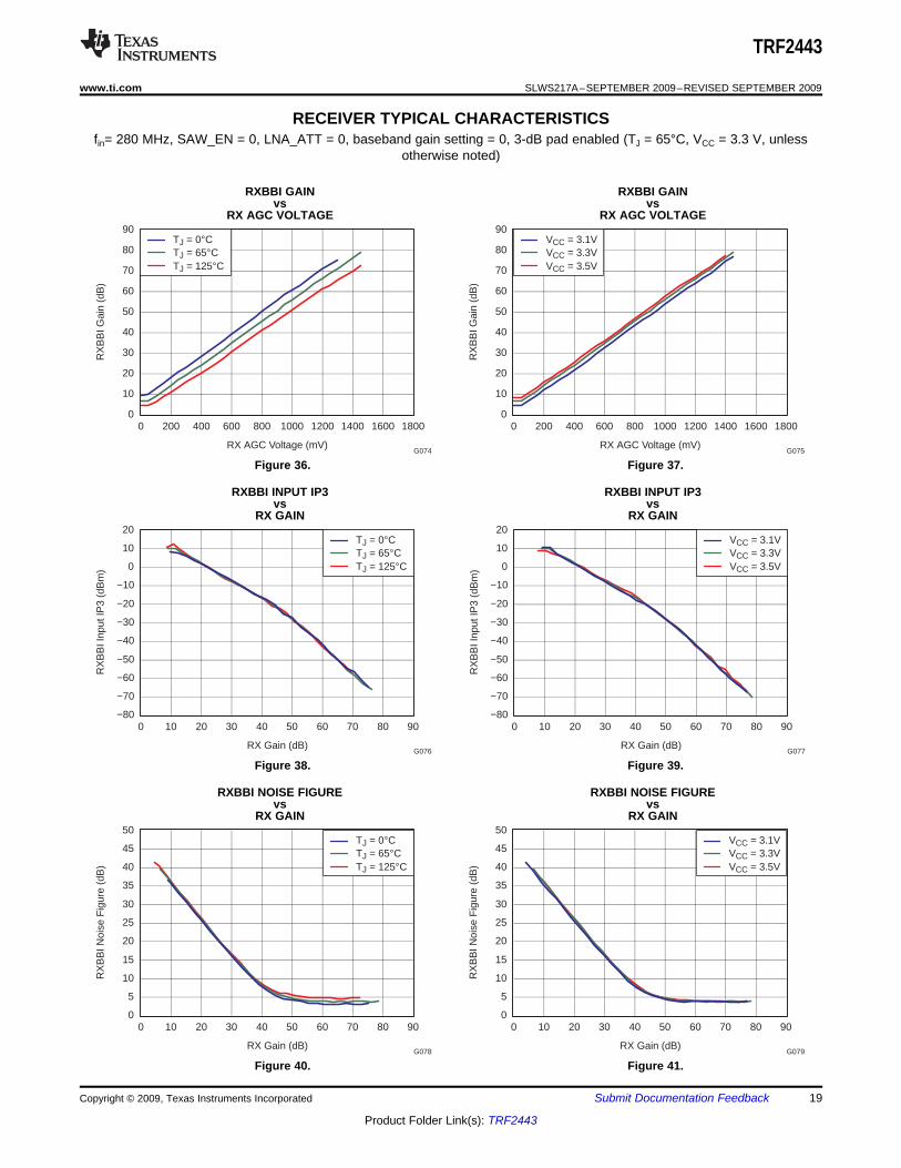
fin= 280 MHz, SAW_EN = 0, LNA_ATT = 0, baseband gain setting = 0, 3-dB pad enabled (TJ = 65°C, VCC = 3.3 V, unlessotherwise noted)
RXBBI GAIN RXBBI GAINvs vs
RX AGC VOLTAGE RX AGC VOLTAGE
Figure 36. Figure 37.
RXBBI INPUT IP3 RXBBI INPUT IP3vs vs
RX GAIN RX GAIN
Figure 38. Figure 39.
RXBBI NOISE FIGURE RXBBI NOISE FIGUREvs vs
RX GAIN RX GAIN
Figure 40. Figure 41.
Copyright © 2009, Texas Instruments Incorporated Submit Documentation Feedback 19
Product Folder Link(s): TRF2443

RECEIVER TYPICAL CHARACTERISTICS
0
10
20
30
40
50
60
70
80
90
0 200 400 600 800 1000 1200 1400 1600 1800
RX
BB
I Gai
n (d
B)
TJ = 0°CTJ = 65°CTJ = 125°C
RX AGC Voltage (mV)G080
0
10
20
30
40
50
60
70
80
90
0 200 400 600 800 1000 1200 1400 1600 1800
RX
BB
I Gai
n (d
B)
VCC = 3.1VVCC = 3.3VVCC = 3.5V
RX AGC Voltage (mV)G081
−80
−70
−60
−50
−40
−30
−20
−10
0
10
20
0 10 20 30 40 50 60 70 80 90
RX
BB
I Inp
ut IP
3 (d
Bm
)
TJ = 0°CTJ = 65°CTJ = 125°C
RX Gain (dB)G082
−80
−70
−60
−50
−40
−30
−20
−10
0
10
20
0 10 20 30 40 50 60 70 80 90
RX
BB
I Inp
ut IP
3 (d
Bm
)
VCC = 3.1VVCC = 3.3VVCC = 3.5V
RX Gain (dB)G083
0
5
10
15
20
25
30
35
40
45
50
0 10 20 30 40 50 60 70 80 90
RX
BB
I Noi
se F
igur
e (d
B)
TJ = 0°CTJ = 65°CTJ = 125°C
RX Gain (dB)G084
0
5
10
15
20
25
30
35
40
45
50
0 10 20 30 40 50 60 70 80 90
RX
BB
I Noi
se F
igur
e (d
B)
VCC = 3.1VVCC = 3.3VVCC = 3.5V
RX Gain (dB)G085
TRF2443
SLWS217A–SEPTEMBER 2009–REVISED SEPTEMBER 2009 ................................................................................................................................... www.ti.com
fin= 280 MHz, SAW_EN = 1, LNA_ATT = 0, baseband gain setting = 9, 3-dB pad disabled (TJ = 65°C, VCC = 3.3 V, unlessotherwise noted)
RXBBI GAIN RXBBI GAINvs vs
RX AGC VOLTAGE RX AGC VOLTAGE
Figure 42. Figure 43.
RXBBI INPUT IP3 RXBBI INPUT IP3vs vs
RX GAIN RX GAIN
Figure 44. Figure 45.
RXBBI NOISE FIGURE RXBBI NOISE FIGUREvs vs
RX GAIN RX GAIN
Figure 46. Figure 47.
20 Submit Documentation Feedback Copyright © 2009, Texas Instruments Incorporated
Product Folder Link(s): TRF2443

RECEIVER LOW-PASS FILTER TYPICAL CHARACTERISTICS
−100
−80
−60
−40
−20
0
RX
Low
-Pas
s F
ilter
Rej
ectio
n (d
B)
0.01 0.1 1 10
BW = 1.8MHz
TJ = 0°CTJ = 65°CTJ = 125°C
Frequency (MHz)G055
−100
−80
−60
−40
−20
0
RX
Low
-Pas
s F
ilter
Rej
ectio
n (d
B)
VCC = 3.1VVCC = 3.3VVCC = 3.5V
0.01 0.1 1 10
BW = 1.8MHz
Frequency (MHz)G056
−100
−80
−60
−40
−20
0
RX
Low
-Pas
s F
ilter
Rej
ectio
n (d
B)
TJ = 0°CTJ = 65°CTJ = 125°C
0.01 0.1 1 10
BW = 2.3MHz
Frequency (MHz)G057
−100
−80
−60
−40
−20
0
RX
Low
-Pas
s F
ilter
Rej
ectio
n (d
B)
VCC = 3.1VVCC = 3.3VVCC = 3.5V
0.01 0.1 1 10
BW = 2.3MHz
Frequency (MHz)G058
−100
−80
−60
−40
−20
0
RX
Low
-Pas
s F
ilter
Rej
ectio
n (d
B)
TJ = 0°CTJ = 65°CTJ = 125°C
0.01 0.1 1 10
BW = 3.5MHz
Frequency (MHz)G059
−100
−80
−60
−40
−20
0
RX
Low
-Pas
s F
ilter
Rej
ectio
n (d
B)
VCC = 3.1VVCC = 3.3VVCC = 3.5V
0.01 0.1 1 10
BW = 3.5MHz
Frequency (MHz)G060
TRF2443
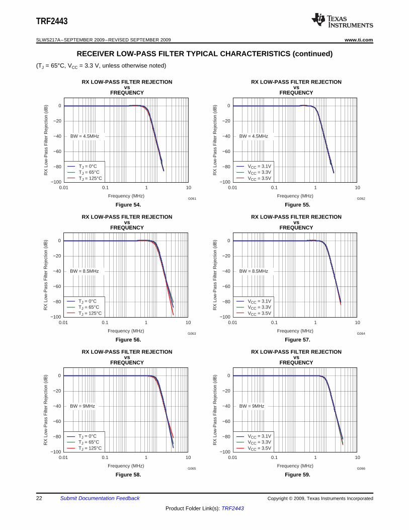
www.ti.com ................................................................................................................................... SLWS217A–SEPTEMBER 2009–REVISED SEPTEMBER 2009
(TJ = 65°C, VCC = 3.3 V, unless otherwise noted)
RX LOW-PASS FILTER REJECTION RX LOW-PASS FILTER REJECTIONvs vs
FREQUENCY FREQUENCY
Figure 48. Figure 49.
RX LOW-PASS FILTER REJECTION RX LOW-PASS FILTER REJECTIONvs vs
FREQUENCY FREQUENCY
Figure 50. Figure 51.
RX LOW-PASS FILTER REJECTION RX LOW-PASS FILTER REJECTIONvs vs
FREQUENCY FREQUENCY
Figure 52. Figure 53.
Copyright © 2009, Texas Instruments Incorporated Submit Documentation Feedback 21
Product Folder Link(s): TRF2443
−100
−80
−60
−40
−20
0
RX
Low
-Pas
s F
ilter
Rej
ectio
n (d
B)
TJ = 0°CTJ = 65°CTJ = 125°C
0.01 0.1 1 10
BW = 4.5MHz
Frequency (MHz)G061
−100
−80
−60
−40
−20
0
RX
Low
-Pas
s F
ilter
Rej
ectio
n (d
B)
VCC = 3.1VVCC = 3.3VVCC = 3.5V
0.01 0.1 1 10
BW = 4.5MHz
Frequency (MHz)G062
−100
−80
−60
−40
−20
0
RX
Low
-Pas
s F
ilter
Rej
ectio
n (d
B)
TJ = 0°CTJ = 65°CTJ = 125°C
0.01 0.1 1 10
BW = 8.5MHz
Frequency (MHz)G063
−100
−80
−60
−40
−20
0
RX
Low
-Pas
s F
ilter
Rej
ectio
n (d
B)
VCC = 3.1VVCC = 3.3VVCC = 3.5V
0.01 0.1 1 10
BW = 8.5MHz
Frequency (MHz)G064
−100
−80
−60
−40
−20
0
RX
Low
-Pas
s F
ilter
Rej
ectio
n (d
B)
TJ = 0°CTJ = 65°CTJ = 125°C
0.01 0.1 1 10
BW = 9MHz
Frequency (MHz)G065
−100
−80
−60
−40
−20
0
RX
Low
-Pas
s F
ilter
Rej
ectio
n (d
B)
VCC = 3.1VVCC = 3.3VVCC = 3.5V
0.01 0.1 1 10
BW = 9MHz
Frequency (MHz)G066
TRF2443
SLWS217A–SEPTEMBER 2009–REVISED SEPTEMBER 2009 ................................................................................................................................... www.ti.com
RECEIVER LOW-PASS FILTER TYPICAL CHARACTERISTICS (continued)(TJ = 65°C, VCC = 3.3 V, unless otherwise noted)
RX LOW-PASS FILTER REJECTION RX LOW-PASS FILTER REJECTIONvs vs
FREQUENCY FREQUENCY
Figure 54. Figure 55.
RX LOW-PASS FILTER REJECTION RX LOW-PASS FILTER REJECTIONvs vs
FREQUENCY FREQUENCY
Figure 56. Figure 57.
RX LOW-PASS FILTER REJECTION RX LOW-PASS FILTER REJECTIONvs vs
FREQUENCY FREQUENCY
Figure 58. Figure 59.
22 Submit Documentation Feedback Copyright © 2009, Texas Instruments Incorporated
Product Folder Link(s): TRF2443
−3.0
−2.5
−2.0
−1.5
−1.0
−0.5
0.0
0.5
RX
Low
-Pas
s F
ilter
Rej
ectio
n (d
B)
TJ = 0°CTJ = 65°CTJ = 125°C
0.01 0.1 1 10
BW = 3.5MHz
Frequency (MHz)G092
−3.0
−2.5
−2.0
−1.5
−1.0
−0.5
0.0
0.5
RX
Low
-Pas
s F
ilter
Rej
ectio
n (d
B)
VCC = 3.1VVCC = 3.3VVCC = 3.5V
0.01 0.1 1 10
BW = 3.5MHz
Frequency (MHz)G093
TRF2443
www.ti.com ................................................................................................................................... SLWS217A–SEPTEMBER 2009–REVISED SEPTEMBER 2009
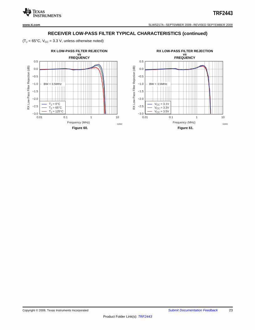
RECEIVER LOW-PASS FILTER TYPICAL CHARACTERISTICS (continued)(TJ = 65°C, VCC = 3.3 V, unless otherwise noted)
RX LOW-PASS FILTER REJECTION RX LOW-PASS FILTER REJECTIONvs vs
FREQUENCY FREQUENCY
Figure 60. Figure 61.
Copyright © 2009, Texas Instruments Incorporated Submit Documentation Feedback 23
Product Folder Link(s): TRF2443

TRANSMITTER TYPICAL CHARACTERISTICS
TX Attenuation Setting (SPI-3, REG1<12,6>)
−35
−30
−25
−20
−15
−10
−5
0
5
10
0 5 10 15 20 25 30 35
TX
Out
put P
ower
(dB
m)
G041
fOUT = 340MHz
TJ = 0°CTJ = 65°CTJ = 125°C
−35
−30
−25
−20
−15
−10
−5
0
5
10
0 5 10 15 20 25 30 35
TX
Out
put P
ower
(dB
m)
VCC = 3.1VVCC = 3.3VVCC = 3.5V
TX Attenuation Setting (SPI-3, REG1<12,6>)G042
fOUT = 340MHz
−20
−15
−10
−5
0
5
10
15
20
25
0 5 10 15 20 25 30 35
TX
Gai
n (d
B)
TJ = 0°CTJ = 65°CTJ = 125°C
TX Attenuation Setting (SPI-3, REG1<12,6>)G043
fOUT = 340MHz−20
−15
−10
−5
0
5
10
15
20
25
0 5 10 15 20 25 30 35
TX
Gai
n (d
B)
VCC = 3.1VVCC = 3.3VVCC = 3.5V
TX Attenuation Setting (SPI-3, REG1<12,6>)G044
fOUT = 340MHz
0.2
0.3
0.4
0.5
0.6
0.7
0.8
0 5 10 15 20 25 30 35
TX
0.5
-dB
Gai
n S
tep
(dB
)
TX Attenuation Setting (SPI-3, REG1<12,6>)G047
TJ = 0°CTJ = 65°CTJ = 125°C fOUT = 340MHz
0.2
0.3
0.4
0.5
0.6
0.7
0.8
0 5 10 15 20 25 30 35
TX
0.5
-dB
Gai
n S
tep
(dB
)
TX Attenuation Setting (SPI-3, REG1<12,6>)G048
fOUT = 340MHz
VCC = 3.1VVCC = 3.3VVCC = 3.5V
TRF2443
SLWS217A–SEPTEMBER 2009–REVISED SEPTEMBER 2009 ................................................................................................................................... www.ti.com
Measured after the transformer (0.7-dB insertion loss) and with a TXBBI/TXBBQ input level of –23 dBVrms (TJ = 65°C,VCC = 3.3 V, unless otherwise noted)
TX OUTPUT POWER TX OUTPUT POWERvs vs
TX ATTENUATION SETTING TX ATTENUATION SETTING
Figure 62. Figure 63.
TX GAIN TX GAINvs vs
TX ATTENUATION SETTING TX ATTENUATION SETTING
Figure 64. Figure 65.
TX 0.5-dB GAIN STEP TX 0.5-dB GAIN STEPvs vs
TX ATTENUATION SETTING TX ATTENUATION SETTING
Figure 66. Figure 67.
24 Submit Documentation Feedback Copyright © 2009, Texas Instruments Incorporated
Product Folder Link(s): TRF2443
0.5
0.6
0.7
0.8
0.9
1.0
1.1
1.2
1.3
1.4
1.5
0 5 10 15 20 25 30 35
TX
1-d
B G
ain
Ste
p (d
B)
TJ = 0°CTJ = 65°CTJ = 125°C
TX Attenuation Setting (SPI-3, REG1<12,6>)G049
fOUT = 340MHz
0.5
0.6
0.7
0.8
0.9
1.0
1.1
1.2
1.3
1.4
1.5
0 5 10 15 20 25 30 35
TX
1-d
B G
ain
Ste
p (d
B)
VCC = 3.1VVCC = 3.3VVCC = 3.5V
TX Attenuation Setting (SPI-3, REG1<12,6>)G050
fOUT = 340MHz
−0.5
−0.4
−0.3
−0.2
−0.1
0.0
0.1
0.2
0.3
0.4
0.5
0 5 10 15 20 25 30 35
TX
Cum
ulat
ive
Gai
n E
rror
(dB
)
TJ = 0°CTJ = 65°CTJ = 125°C
TX Attenuation Setting (SPI-3, REG1<12,6>)G090
fOUT = 340MHz
−0.5
−0.4
−0.3
−0.2
−0.1
0.0
0.1
0.2
0.3
0.4
0.5
0 5 10 15 20 25 30 35
TX
Cum
ulat
ive
Gai
n E
rror
(dB
)
VCC = 3.1VVCC = 3.3VVCC = 3.5V
TX Attenuation Setting (SPI-3, REG1<12,6>)G091
fOUT = 340MHz
30
35
40
45
50
55
60
0 5 10 15 20 25 30 35Unc
alib
rate
d T
X S
ideb
and
Sup
pres
sion
(dB
)
TJ = 0°CTJ = 65°CTJ = 125°C
TX Attenuation Setting (SPI-3, REG1<12,6>)G051
fOUT = 340MHz
30
35
40
45
50
55
60
0 5 10 15 20 25 30 35Unc
alib
rate
d T
X S
ideb
and
Sup
pres
sion
(dB
)
VCC = 3.1VVCC = 3.3VVCC = 3.5V
TX Attenuation Setting (SPI-3, REG1<12,6>)G052
fOUT = 340MHz
TRF2443
www.ti.com ................................................................................................................................... SLWS217A–SEPTEMBER 2009–REVISED SEPTEMBER 2009
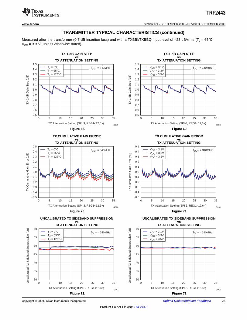
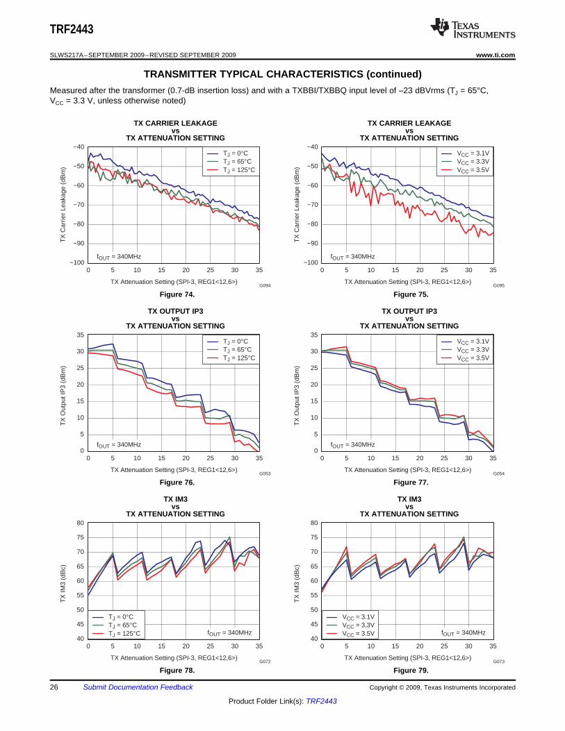
TRANSMITTER TYPICAL CHARACTERISTICS (continued)Measured after the transformer (0.7-dB insertion loss) and with a TXBBI/TXBBQ input level of –23 dBVrms (TJ = 65°C,VCC = 3.3 V, unless otherwise noted)
TX 1-dB GAIN STEP TX 1-dB GAIN STEPvs vs
TX ATTENUATION SETTING TX ATTENUATION SETTING
Figure 68. Figure 69.
TX CUMULATIVE GAIN ERROR TX CUMULATIVE GAIN ERRORvs vs
TX ATTENUATION SETTING TX ATTENUATION SETTING
Figure 70. Figure 71.
UNCALIBRATED TX SIDEBAND SUPPRESSION UNCALIBRATED TX SIDEBAND SUPPRESSIONvs vs
TX ATTENUATION SETTING TX ATTENUATION SETTING
Figure 72. Figure 73.
Copyright © 2009, Texas Instruments Incorporated Submit Documentation Feedback 25
Product Folder Link(s): TRF2443
−100
−90
−80
−70
−60
−50
−40
0 5 10 15 20 25 30 35
TX
Car
rier
Leak
age
(dB
m)
TX Attenuation Setting (SPI-3, REG1<12,6>)G094
TJ = 0°CTJ = 65°CTJ = 125°C
fOUT = 340MHz−100
−90
−80
−70
−60
−50
−40
0 5 10 15 20 25 30 35
TX
Car
rier
Leak
age
(dB
m)
TX Attenuation Setting (SPI-3, REG1<12,6>)G095
VCC = 3.1VVCC = 3.3VVCC = 3.5V
fOUT = 340MHz
0
5
10
15
20
25
30
35
0 5 10 15 20 25 30 35
TX
Out
put I
P3
(dB
m)
TJ = 0°CTJ = 65°CTJ = 125°C
TX Attenuation Setting (SPI-3, REG1<12,6>)G053
fOUT = 340MHz0
5
10
15
20
25
30
35
0 5 10 15 20 25 30 35
TX
Out
put I
P3
(dB
m)
VCC = 3.1VVCC = 3.3VVCC = 3.5V
TX Attenuation Setting (SPI-3, REG1<12,6>)G054
fOUT = 340MHz
40
45
50
55
60
65
70
75
80
0 5 10 15 20 25 30 35
TX
IM3
(dB
c)
TJ = 0°CTJ = 65°CTJ = 125°C
TX Attenuation Setting (SPI-3, REG1<12,6>)G072
fOUT = 340MHz40
45
50
55
60
65
70
75
80
0 5 10 15 20 25 30 35
TX
IM3
(dB
c)
VCC = 3.1VVCC = 3.3VVCC = 3.5V
TX Attenuation Setting (SPI-3, REG1<12,6>)G073
fOUT = 340MHz
TRF2443
SLWS217A–SEPTEMBER 2009–REVISED SEPTEMBER 2009 ................................................................................................................................... www.ti.com
TRANSMITTER TYPICAL CHARACTERISTICS (continued)Measured after the transformer (0.7-dB insertion loss) and with a TXBBI/TXBBQ input level of –23 dBVrms (TJ = 65°C,VCC = 3.3 V, unless otherwise noted)
TX CARRIER LEAKAGE TX CARRIER LEAKAGEvs vs
TX ATTENUATION SETTING TX ATTENUATION SETTING
Figure 74. Figure 75.
TX OUTPUT IP3 TX OUTPUT IP3vs vs
TX ATTENUATION SETTING TX ATTENUATION SETTING
Figure 76. Figure 77.
TX IM3 TX IM3vs vs
TX ATTENUATION SETTING TX ATTENUATION SETTING
Figure 78. Figure 79.
26 Submit Documentation Feedback Copyright © 2009, Texas Instruments Incorporated
Product Folder Link(s): TRF2443
Time (µs)
−80
−70
−60
−50
−40
−30
−20
−10
0
10
0 10 20 30 40 50 60 70 80 90 100
TX
Out
put P
ower
(dB
m)
G067
SPI-3 REG3<10,9>=<10>
TJ = 0°CTJ = 65°CTJ = 125°C
−80
−70
−60
−50
−40
−30
−20
−10
0
10
0 10 20 30 40 50 60 70 80 90 100
TX
Out
put P
ower
(dB
m)
VCC = 3.1VVCC = 3.3VVCC = 3.5V
Time (µs)G068
SPI-3 REG3<10,9>=<10>
−170
−165
−160
−155
−150
−145
−140
−135
−130
−125
−120
0 5 10 15 20 25 30
TX
Out
put N
oise
(dB
m/H
z)
VCC = 3.1VVCC = 3.3VVCC = 3.5V
TX Attenuation Setting (SPI-3, REG1<12,6>)G069
Note: No Input Signal
TRF2443
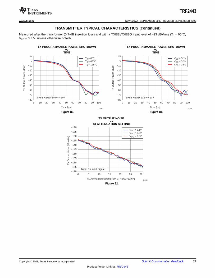
www.ti.com ................................................................................................................................... SLWS217A–SEPTEMBER 2009–REVISED SEPTEMBER 2009
TRANSMITTER TYPICAL CHARACTERISTICS (continued)Measured after the transformer (0.7-dB insertion loss) and with a TXBBI/TXBBQ input level of –23 dBVrms (TJ = 65°C,VCC = 3.3 V, unless otherwise noted)
TX PROGRAMMABLE POWER-SHUTDOWN TX PROGRAMMABLE POWER-SHUTDOWNvs vs
TIME TIME
Figure 80. Figure 81.
TX OUTPUT NOISEvs
TX ATTENUATION SETTING
Figure 82.
Copyright © 2009, Texas Instruments Incorporated Submit Documentation Feedback 27
Product Folder Link(s): TRF2443
PLL TYPICAL CHARACTERISTICS
−160
−150
−140
−130
−120
−110
−100
−90
Pha
se N
oise
(dB
c/H
z)
0.01 0.1 1 100
BW = 2720MHz
Frequency Offset (MHz)G096
10
TJ = 0°CTJ = 65°CTJ = 125°C
−160
−150
−140
−130
−120
−110
−100
−90
Pha
se N
oise
(dB
c/H
z)
0.01 0.1 1 100
BW = 2720MHz
Frequency Offset (MHz)G097
10
VCC = 3.1VVCC = 3.3VVCC = 3.5V
−160
−150
−140
−130
−120
−110
−100
−90
Pha
se N
oise
(dB
c/H
z)
0.01 0.1 1 100
BW = 2240MHz
Frequency Offset (MHz)G098
10
TJ = 0°CTJ = 65°CTJ = 125°C
−160
−150
−140
−130
−120
−110
−100
−90P
hase
Noi
se (
dBc/
Hz)
0.01 0.1 1 100
BW = 2240MHz
Frequency Offset (MHz)G099
10
VCC = 3.1VVCC = 3.3VVCC = 3.5V
TRF2443
SLWS217A–SEPTEMBER 2009–REVISED SEPTEMBER 2009 ................................................................................................................................... www.ti.com
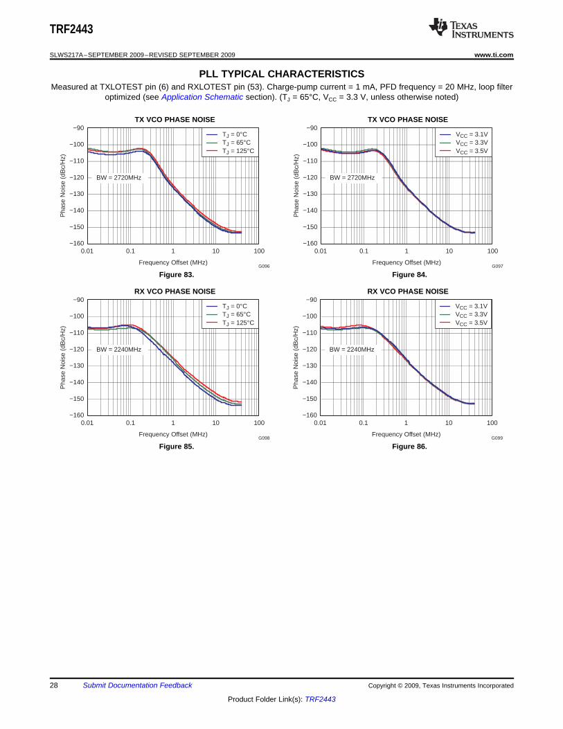
Measured at TXLOTEST pin (6) and RXLOTEST pin (53). Charge-pump current = 1 mA, PFD frequency = 20 MHz, loop filteroptimized (see Application Schematic section). (TJ = 65°C, VCC = 3.3 V, unless otherwise noted)
TX VCO PHASE NOISE TX VCO PHASE NOISE
Figure 83. Figure 84.
RX VCO PHASE NOISE RX VCO PHASE NOISE
Figure 85. Figure 86.
28 Submit Documentation Feedback Copyright © 2009, Texas Instruments Incorporated
Product Folder Link(s): TRF2443
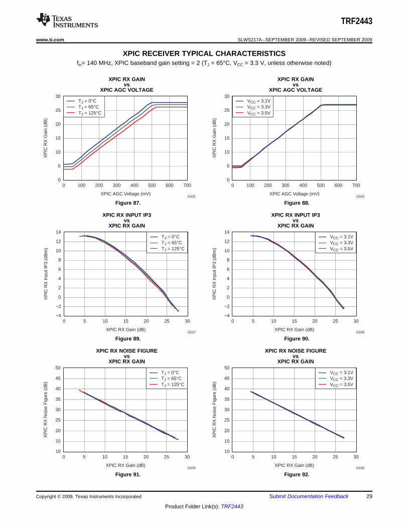
XPIC RECEIVER TYPICAL CHARACTERISTICS
XPIC AGC Voltage (mV)
0
5
10
15
20
25
30
0 100 200 300 400 500 600 700
XP
IC R
X G
ain
(dB
)
G025
TJ = 0°CTJ = 65°CTJ = 125°C
0
5
10
15
20
25
30
0 100 200 300 400 500 600 700
XP
IC R
X G
ain
(dB
)
VCC = 3.1VVCC = 3.3VVCC = 3.5V
XPIC AGC Voltage (mV)G026
XPIC RX Gain (dB)
−4
−2
0
2
4
6
8
10
12
14
0 5 10 15 20 25 30
XP
IC R
X In
put I
P3
(dB
m)
G027
TJ = 0°CTJ = 65°CTJ = 125°C
−4
−2
0
2
4
6
8
10
12
14
0 5 10 15 20 25 30
XP
IC R
X In
put I
P3
(dB
m)
VCC = 3.1VVCC = 3.3VVCC = 3.5V
XPIC RX Gain (dB)G028
10
15
20
25
30
35
40
45
50
0 5 10 15 20 25 30
XP
IC R
X N
oise
Fig
ure
(dB
)
TJ = 0°CTJ = 65°CTJ = 125°C
XPIC RX Gain (dB)G029
10
15
20
25
30
35
40
45
50
0 5 10 15 20 25 30
XP
IC R
X N
oise
Fig
ure
(dB
)
VCC = 3.1VVCC = 3.3VVCC = 3.5V
XPIC RX Gain (dB)G030
TRF2443
www.ti.com ................................................................................................................................... SLWS217A–SEPTEMBER 2009–REVISED SEPTEMBER 2009
fin= 140 MHz, XPIC baseband gain setting = 2 (TJ = 65°C, VCC = 3.3 V, unless otherwise noted)
XPIC RX GAIN XPIC RX GAINvs vs
XPIC AGC VOLTAGE XPIC AGC VOLTAGE
Figure 87. Figure 88.
XPIC RX INPUT IP3 XPIC RX INPUT IP3vs vs
XPIC RX GAIN XPIC RX GAIN
Figure 89. Figure 90.
XPIC RX NOISE FIGURE XPIC RX NOISE FIGUREvs vs
XPIC RX GAIN XPIC RX GAIN
Figure 91. Figure 92.
Copyright © 2009, Texas Instruments Incorporated Submit Documentation Feedback 29
Product Folder Link(s): TRF2443
INSERTION LOSSES TYPICAL CHARACTERISTICS
Frequency (MHz)
−35
−30
−25
−20
−15
−10
90 100 110 120 130 140 150 160 170 180 190
Inpu
t Ret
urn
Loss
XP
ICIN
(dB
)
G031
VCC = 3.1VVCC = 3.3VVCC = 3.5V
−35
−30
−25
−20
−15
−10
90 100 110 120 130 140 150 160 170 180 190
Out
put R
etur
n Lo
ss X
PIC
OU
T (
dB) VCC = 3.1V
VCC = 3.3VVCC = 3.5V
Frequency (MHz)G032
−35
−30
−25
−20
−15
−10
90 100 110 120 130 140 150 160 170 180 190
Inpu
t Ret
urn
Loss
IFIN
(dB
)
VCC = 3.1VVCC = 3.3VVCC = 3.5V
Frequency (MHz)G033
−35
−30
−25
−20
−15
−10
90 100 110 120 130 140 150 160 170 180 190
Out
put R
etur
n Lo
ss IF
OU
T (
dB)
VCC = 3.1VVCC = 3.3VVCC = 3.5V
Frequency (MHz)G034
−40
−35
−30
−25
−20
−15
−10
90 100 110 120 130 140 150 160 170 180 190
Inpu
t Ret
urn
Loss
RX
IN (
dB)
LNA_ATTN = 0LAN_ATTN = 3
LNA_ATTN = 6LAN_ATTN = 9
LNA_ATTN = 12LAN_ATTN = 15
LNA_ATTN = 18
Frequency (MHz)G035
−35
−30
−25
−20
−15
−10
−5
0
300 310 320 330 340 350 360 370 380
Out
put R
etur
n Lo
ss T
XO
UT
(dB
)
VCC = 3.1VVCC = 3.3VVCC = 3.5V
Frequency (MHz)G036
TRF2443
SLWS217A–SEPTEMBER 2009–REVISED SEPTEMBER 2009 ................................................................................................................................... www.ti.com
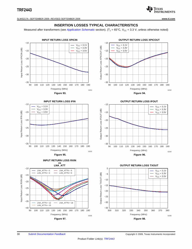
Measured after transformers (see Application Schematic section). (TJ = 65°C, VCC = 3.3 V, unless otherwise noted)
INPUT RETURN LOSS XPICIN OUTPUT RETURN LOSS XPICOUT
Figure 93. Figure 94.
INPUT RETURN LOSS IFIN OUTPUT RETURN LOSS IFOUT
Figure 95. Figure 96.
INPUT RETURN LOSS RXINvs
LNA_ATT OUTPUT RETURN LOSS TXOUT
Figure 97. Figure 98.
30 Submit Documentation Feedback Copyright © 2009, Texas Instruments Incorporated
Product Folder Link(s): TRF2443

SPI REGISTERS
“End of Write Cycle”pulse
1stWriteclockpulse
tsu1 th t(CLK)
32nd
Writeclockpulse
tt susu 23 tw
CLOCK
DATA
RE
GIS
TE
RW
RIT
E
t(CL)
t (CH)
LATCH
ENABLE
DB30DB29DB2
Address Bit2DB1
Address Bit1DB0 (LSB)
Address Bit0
DB3Address Bit3 DB31(MSB)
TRF2443 Addressing Scheme
TRF2443
www.ti.com ................................................................................................................................... SLWS217A–SEPTEMBER 2009–REVISED SEPTEMBER 2009
The TRF2443 features a three-wire serial programming interface (SPI) that controls an internal 32-bit shiftregister. There are a total of three signals that must be applied: the clock (CLKSPI), the serial data (DATASPI)and the latch enable (LESPI). The TRF2443 has an additional pin (RDBKSPI) for readback functionality. This pinis a digital pin and can be used to read back values of different internal registers.
The DATA (DB0–DB31) is loaded LSB-first and is read on the rising edge of the CLOCK. The latch enable isasynchronous to the CLOCK, and at its rising edge the data in the shift register is loaded onto the selectedinternal register. The 5 LSBs of the data field are the address bits to select the available internal registers (seeFigure 99).
The SPI can operate reliably at clock speeds up to 20 MHz (clock period <50 ns). In theory, two 32-bit registerscould be programmed within 3.3 µs (64 clock cycles at 50 ns per clock cycle plus setup times). However, theuser must exercise care when writing consecutive registers to ensure that subsequent register writes do notdisrupt a previously requested operation such as a calibration. Calibration times are functions of the externalreference frequency used as well as internally programmable clock dividers set by the user. The applicationsection of this data sheet describes how to determine these calibration times. The user should allow for suchcalibration times when writing registers to the serial interface that contain settings related to the calibration orsettings related to the circuits which are being calibrated.
Figure 99. SPI Timing Diagram
Table 1. SPI Timing – Writing PhaseSYMBOL PARAMETER MIN TYP MAX UNITS
th Hold time, data to clock 20 nstSU1 Setup time, data to clock 20 nst(CL) Clock low duration 20 nst(CH) Clock high duration 20 nstSU2 Setup time, clock to enable 20 nstW Enable Time 50 nst(CLK) Clock period 50 nstSU3 Setup time, latch to data 70 ns
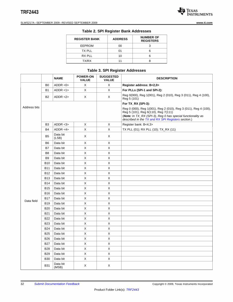
The TRF2443 has a separate set of register banks for the EEPROM (SPI-0), TX PLL (SPI-1), RX PLL (SPI-2),and TX/RX functionality (SPI-3). Each of the register banks has unique address bits to identify it, and within eachregister bank there are several registers which require an additional 3 bits of addressing.
Each register is 32 bits long; the bits can be described by B<31,0>. The 5 LSBs of each register, (B<4,0>), arethe address bits, with B<4,3> corresponding to the address of the register bank and B<2,0> corresponding to theaddress of the individual register within each bank (see Table 2).
Copyright © 2009, Texas Instruments Incorporated Submit Documentation Feedback 31
Product Folder Link(s): TRF2443
TRF2443
SLWS217A–SEPTEMBER 2009–REVISED SEPTEMBER 2009 ................................................................................................................................... www.ti.com
Table 2. SPI Register Bank AddressesNUMBER OFREGISTER BANK ADDRESS REGISTERS
EEPROM 00 3TX PLL 01 6RX PLL 10 6TX/RX 11 8
Table 3. SPI Register AddressesPOWER-ON SUGGESTEDNAME DESCRIPTIONVALUE VALUE
B0 ADDR <0> X X Register address: B<2,0>B1 ADDR <1> X X For PLLs (SPI-1 and SPI-2):
Reg 0(000), Reg 1(001), Reg 2 (010), Reg 3 (011), Reg 4 (100),B2 ADDR <2> X X Reg 5 (101)For TX_RX (SPI-3):
Address bits Reg 0 (000), Reg 1(001), Reg 2 (010), Reg 3 (011), Reg 4 (100),Reg 5 (101), Reg 6(110), Reg 7(111)(Note: In TX_RX (SPI-3), Reg 0 has special functionality asdescribed in the TX and RX SPI Registers section.)
B3 ADDR <3> X X Register bank: B<4,3>B4 ADDR <4> X X TX PLL (01); RX PLL (10); TX_RX (11)
Data bitB5 X X(LSB)B6 Data bit X XB7 Data bit X XB8 Data bit X XB9 Data bit X XB10 Data bit X XB11 Data bit X XB12 Data bit X XB13 Data bit X XB14 Data bit X XB15 Data bit X XB16 Data bit X XB17 Data bit X X
Data fieldB19 Data bit X XB20 Data bit X XB21 Data bit X XB22 Data bit X XB23 Data bit X XB24 Data bit X XB25 Data bit X XB26 Data bit X XB27 Data bit X XB28 Data bit X XB29 Data bit X XB30 Data bit X X
Data bitB31 X X(MSB)
32 Submit Documentation Feedback Copyright © 2009, Texas Instruments Incorporated
Product Folder Link(s): TRF2443

TX Synthesizer SPI registers
TRF2443
www.ti.com ................................................................................................................................... SLWS217A–SEPTEMBER 2009–REVISED SEPTEMBER 2009
SPI1 Register 1Register address SPI address TX reference divider
Bit0 Bit1 Bit2 Bit3 Bit4 Bit5 Bit6 Bit7 Bit8 Bit9 Bit10 Bit11 Bit12 Bit13 Bit14 Bit15
TX reference divider REF VCO TX charge-pump current TX CP RSV RSB CP OFF CP UP CP DNINV NEG DOUBLE
Bit16 Bit17 Bit18 Bit19 Bit20 Bit21 Bit22 Bit23 Bit24 Bit25 Bit26 Bit27 Bit28 Bit29 Bit30 Bit31
REGISTER POWER-ON SUGGESTEDNAME DESCRIPTION1 VALUE VALUEBit0 ADDR_0 1 1 Register address bitsBit1 ADDR_1 0 0Bit2 ADDR_2 0 0Bit3 ADDR_3 1 1 SPI address bitsBit4 ADDR_4 0 0Bit5 TXRDIV_0 0 App. specificBit6 TXRDIV_1 0 App. specific 14-bit reference divider value
(minimum value Rmin = 1;Bit7 TXRDIV_2 0 App. specific maximum value Rmax = 16,383)Bit8 TXRDIV_3 0 App. specificBit9 TXRDIV_4 0 App. specific
Bit10 TXRDIV_5 0 App. specificBit11 TXRDIV_6 0 App. specificBit12 TXRDIV_7 0 App. specificBit13 TXRDIV_8 0 App. specificBit14 TXRDIV_9 0 App. specificBit15 TXRDIV_10 0 App. specificBit16 TXRDIV_11 0 App. specificBit17 TXRDIV_12 0 App. specificBit18 TXRDIV_13 0 App. specificBit19 TXREF_INV 0 0 Invert reference-clock polarity; 1 = use falling edgeBit20 TXNEG_VCO 1 1 VCO polarity control; 1 = negative slope (negative Kv)Bit21 TXICP_0 0 0 Program charge-pump dc current, ICP, from 0.5 mA (1 1111) to 2 mA
(0 0000);Bit22 TXICP_1 1 1default value 1 mA (0 1010)
Bit23 TXICP_2 0 0Bit24 TXICP_3 1 1Bit25 TXICP_4 0 0Bit26 TXICPDOUBLE 0 0 1 = set ICP to double the currentBit27 RSV 0 0 ReservedBit28 RSV 0 0 ReservedBit29 TXCP_OVERRIDE 0 0 1 = disable charge pumpBit30 TXCP_UP 0 0 1 = enable the charge-pump source current in disable modeBit31 TXCP_DN 0 0 1 = enable the charge-pump sink current in disable mode
Copyright © 2009, Texas Instruments Incorporated Submit Documentation Feedback 33
Product Folder Link(s): TRF2443
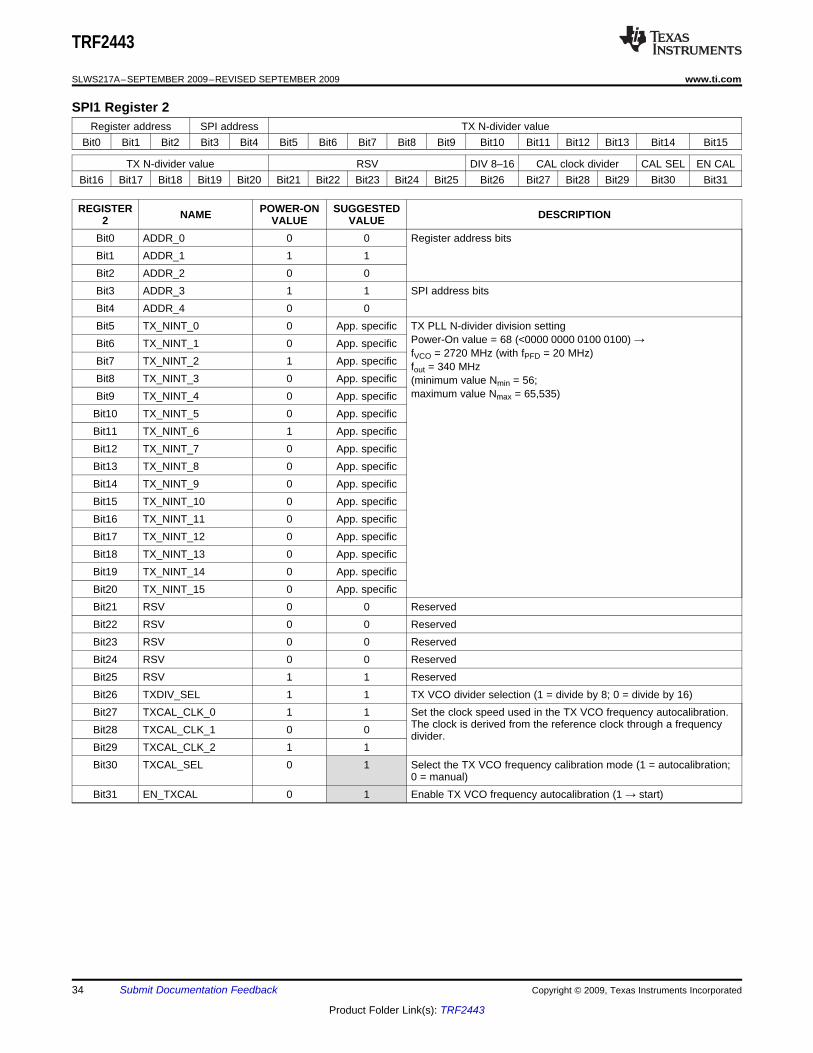
TRF2443
SLWS217A–SEPTEMBER 2009–REVISED SEPTEMBER 2009 ................................................................................................................................... www.ti.com
SPI1 Register 2Register address SPI address TX N-divider value
Bit0 Bit1 Bit2 Bit3 Bit4 Bit5 Bit6 Bit7 Bit8 Bit9 Bit10 Bit11 Bit12 Bit13 Bit14 Bit15
TX N-divider value RSV DIV 8–16 CAL clock divider CAL SEL EN CALBit16 Bit17 Bit18 Bit19 Bit20 Bit21 Bit22 Bit23 Bit24 Bit25 Bit26 Bit27 Bit28 Bit29 Bit30 Bit31
REGISTER POWER-ON SUGGESTEDNAME DESCRIPTION2 VALUE VALUEBit0 ADDR_0 0 0 Register address bitsBit1 ADDR_1 1 1Bit2 ADDR_2 0 0Bit3 ADDR_3 1 1 SPI address bitsBit4 ADDR_4 0 0Bit5 TX_NINT_0 0 App. specific TX PLL N-divider division setting
Power-On value = 68 (<0000 0000 0100 0100) →Bit6 TX_NINT_1 0 App. specificfVCO = 2720 MHz (with fPFD = 20 MHz)
Bit7 TX_NINT_2 1 App. specific fout = 340 MHzBit8 TX_NINT_3 0 App. specific (minimum value Nmin = 56;
maximum value Nmax = 65,535)Bit9 TX_NINT_4 0 App. specificBit10 TX_NINT_5 0 App. specificBit11 TX_NINT_6 1 App. specificBit12 TX_NINT_7 0 App. specificBit13 TX_NINT_8 0 App. specificBit14 TX_NINT_9 0 App. specificBit15 TX_NINT_10 0 App. specificBit16 TX_NINT_11 0 App. specificBit17 TX_NINT_12 0 App. specificBit18 TX_NINT_13 0 App. specificBit19 TX_NINT_14 0 App. specificBit20 TX_NINT_15 0 App. specificBit21 RSV 0 0 ReservedBit22 RSV 0 0 ReservedBit23 RSV 0 0 ReservedBit24 RSV 0 0 ReservedBit25 RSV 1 1 ReservedBit26 TXDIV_SEL 1 1 TX VCO divider selection (1 = divide by 8; 0 = divide by 16)Bit27 TXCAL_CLK_0 1 1 Set the clock speed used in the TX VCO frequency autocalibration.
The clock is derived from the reference clock through a frequencyBit28 TXCAL_CLK_1 0 0 divider.Bit29 TXCAL_CLK_2 1 1Bit30 TXCAL_SEL 0 1 Select the TX VCO frequency calibration mode (1 = autocalibration;
0 = manual)Bit31 EN_TXCAL 0 1 Enable TX VCO frequency autocalibration (1 → start)
34 Submit Documentation Feedback Copyright © 2009, Texas Instruments Incorporated
Product Folder Link(s): TRF2443

TRF2443
www.ti.com ................................................................................................................................... SLWS217A–SEPTEMBER 2009–REVISED SEPTEMBER 2009
TXCAL_CLK<2,0>: Set the frequency divider value used to derive the TX VCO calibration clock from thereference clock (See Table 4)
Table 4. TX VCO Calibration ClockDivider vs TXCAL_CLK<2,0>
TXCAL_CLK FREQUENCY DIVIDER000 1001 8010 16011 128100 256101 1024110 2048111 16,684
SPI1 Register 4Register address SPI address RSV RSV RSV RSV RSV RSV Power down TX PLL blocks RSV
Bit0 Bit1 Bit2 Bit3 Bit4 Bit5 Bit6 Bit7 Bit8 Bit9 Bit10 Bit11 Bit12 Bit13 Bit14 Bit15
RSV Power down TX PLL blocks RSV RSV RSV TXVCO trimBit16 Bit17 Bit18 Bit19 Bit20 Bit21 Bit22 Bit23 Bit24 Bit25 Bit26 Bit27 Bit28 Bit29 Bit30 Bit31
REGISTER POWER-ON SUGGESTEDNAME DESCRIPTION4 VALUE VALUEBit0 ADDR_0 0 0 Register address bitsBit1 ADDR_1 0 0Bit2 ADDR_2 1 1Bit3 ADDR_3 1 1 SPI address bitsBit4 ADDR_4 0 0Bit5 RSV 0 0 ReservedBit6 RSV 0 0 ReservedBit7 RSV 0 0 ReservedBit8 RSV 0 0 ReservedBit9 RSV 1 1 Reserved
Bit10 RSV 1 1 ReservedBit11 PWD_TXCP 0 0 When 1, TX charge pump is offBit12 PWD_TXVCO 0 0 When 1, TX VCO is offBit13 PWD_TXBUF1 0 0 Power down VCO buffer 1 (1 = off)Bit14 PWD_TXBUF2 0 0 Power down VCO buffer 2 (1 = off)Bit15 RSV 1 1 ReservedBit16 PWD_TX_TESTBUF 0 1 Power down TXVCO output buffer, pin TXLOTEST (1 = off)Bit17 PWD_TXDIV2 0 0 Power down VCO divider (1 = off)Bit18 PWD_TXPRESC 0 0 Power down prescaler buffer (1 = off)Bit19 PWD_TXRESYNC 0 0 Power down re-synch D flip-flop (1 = off)Bit20 PWD_TXPLL 0 0 Power down whole TX PLL (1 = off)Bit21 PWD_TXDIV 0 0 Power down LO divider (1 = off)Bit22 PWD_TXDET 0 0 Power down VCO detector (1 = off; used for VCO calibration)Bit23 RSV 0 0 ReservedBit24 RSV 0 0 ReservedBit25 RSV 0 0 Reserved
Copyright © 2009, Texas Instruments Incorporated Submit Documentation Feedback 35
Product Folder Link(s): TRF2443
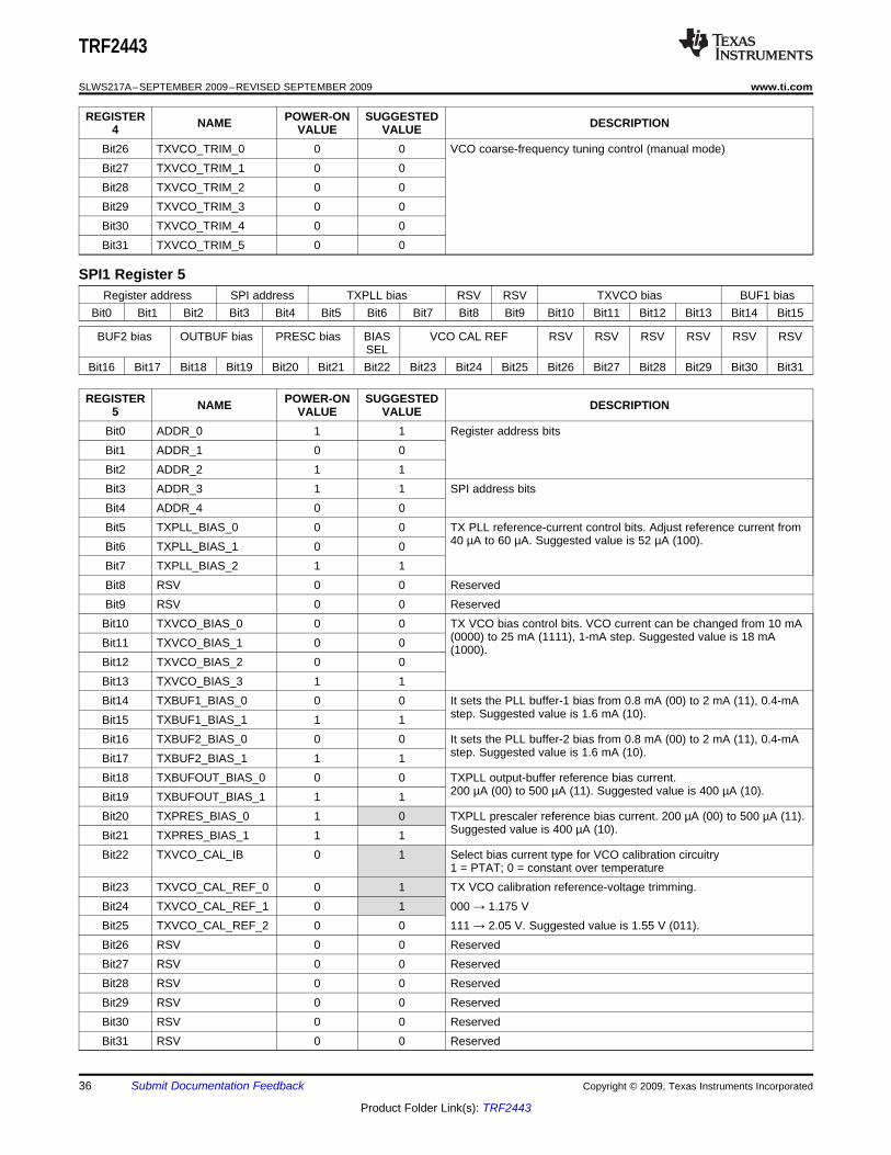
TRF2443
SLWS217A–SEPTEMBER 2009–REVISED SEPTEMBER 2009 ................................................................................................................................... www.ti.com
REGISTER POWER-ON SUGGESTEDNAME DESCRIPTION4 VALUE VALUEBit26 TXVCO_TRIM_0 0 0 VCO coarse-frequency tuning control (manual mode)Bit27 TXVCO_TRIM_1 0 0Bit28 TXVCO_TRIM_2 0 0Bit29 TXVCO_TRIM_3 0 0Bit30 TXVCO_TRIM_4 0 0Bit31 TXVCO_TRIM_5 0 0
SPI1 Register 5Register address SPI address TXPLL bias RSV RSV TXVCO bias BUF1 bias
Bit0 Bit1 Bit2 Bit3 Bit4 Bit5 Bit6 Bit7 Bit8 Bit9 Bit10 Bit11 Bit12 Bit13 Bit14 Bit15
BUF2 bias OUTBUF bias PRESC bias BIAS VCO CAL REF RSV RSV RSV RSV RSV RSVSEL
Bit16 Bit17 Bit18 Bit19 Bit20 Bit21 Bit22 Bit23 Bit24 Bit25 Bit26 Bit27 Bit28 Bit29 Bit30 Bit31
REGISTER POWER-ON SUGGESTEDNAME DESCRIPTION5 VALUE VALUEBit0 ADDR_0 1 1 Register address bitsBit1 ADDR_1 0 0Bit2 ADDR_2 1 1Bit3 ADDR_3 1 1 SPI address bitsBit4 ADDR_4 0 0Bit5 TXPLL_BIAS_0 0 0 TX PLL reference-current control bits. Adjust reference current from
40 µA to 60 µA. Suggested value is 52 µA (100).Bit6 TXPLL_BIAS_1 0 0Bit7 TXPLL_BIAS_2 1 1Bit8 RSV 0 0 ReservedBit9 RSV 0 0 Reserved
Bit10 TXVCO_BIAS_0 0 0 TX VCO bias control bits. VCO current can be changed from 10 mA(0000) to 25 mA (1111), 1-mA step. Suggested value is 18 mABit11 TXVCO_BIAS_1 0 0 (1000).
Bit12 TXVCO_BIAS_2 0 0Bit13 TXVCO_BIAS_3 1 1Bit14 TXBUF1_BIAS_0 0 0 It sets the PLL buffer-1 bias from 0.8 mA (00) to 2 mA (11), 0.4-mA
step. Suggested value is 1.6 mA (10).Bit15 TXBUF1_BIAS_1 1 1Bit16 TXBUF2_BIAS_0 0 0 It sets the PLL buffer-2 bias from 0.8 mA (00) to 2 mA (11), 0.4-mA
step. Suggested value is 1.6 mA (10).Bit17 TXBUF2_BIAS_1 1 1Bit18 TXBUFOUT_BIAS_0 0 0 TXPLL output-buffer reference bias current.
200 µA (00) to 500 µA (11). Suggested value is 400 µA (10).Bit19 TXBUFOUT_BIAS_1 1 1Bit20 TXPRES_BIAS_0 1 0 TXPLL prescaler reference bias current. 200 µA (00) to 500 µA (11).
Suggested value is 400 µA (10).Bit21 TXPRES_BIAS_1 1 1Bit22 TXVCO_CAL_IB 0 1 Select bias current type for VCO calibration circuitry
1 = PTAT; 0 = constant over temperatureBit23 TXVCO_CAL_REF_0 0 1 TX VCO calibration reference-voltage trimming.Bit24 TXVCO_CAL_REF_1 0 1 000 → 1.175 VBit25 TXVCO_CAL_REF_2 0 0 111 → 2.05 V. Suggested value is 1.55 V (011).Bit26 RSV 0 0 ReservedBit27 RSV 0 0 ReservedBit28 RSV 0 0 ReservedBit29 RSV 0 0 ReservedBit30 RSV 0 0 ReservedBit31 RSV 0 0 Reserved
36 Submit Documentation Feedback Copyright © 2009, Texas Instruments Incorporated
Product Folder Link(s): TRF2443

RX Synthesizer SPI registers
TRF2443
www.ti.com ................................................................................................................................... SLWS217A–SEPTEMBER 2009–REVISED SEPTEMBER 2009
SPI2 Register 1Register address SPI address RX reference divider
Bit0 Bit1 Bit2 Bit3 Bit4 Bit5 Bit6 Bit7 Bit8 Bit9 Bit10 Bit11 Bit12 Bit13 Bit14 Bit15
— REF VCO RX charge-pump current RX CP RSV RSV CP CP CPINV NEG DOUBLE OFF UP DN
Bit16 Bit17 Bit18 Bit19 Bit20 Bit21 Bit22 Bit23 Bit24 Bit25 Bit26 Bit27 Bit28 Bit29 Bit30 Bit31
REGISTER POWER-ON SUGGESTEDNAME DESCRIPTION1 VALUE VALUEBit0 ADDR_0 1 1 Register address bitsBit1 ADDR_1 0 0Bit2 ADDR_2 0 0Bit3 ADDR_3 0 0 SPI address bitsBit4 ADDR_4 1 1Bit5 RXRDIV_0 0 App. specificBit6 RXRDIV_1 0 App. specific 14-bit reference-divider value
(minimum value Rmin = 1;Bit7 RXRDIV_2 0 App. specific maximum value Rmax = 16,383)Bit8 RXRDIV_3 0 App. specificBit9 RXRDIV_4 0 App. specific
Bit10 RXRDIV_5 0 App. specificBit11 RXRDIV_6 0 App. specificBit12 RXRDIV_7 0 App. specificBit13 RXRDIV_8 0 App. specificBit14 RXRDIV_9 0 App. specificBit15 RXRDIV_10 0 App. specificBit16 RXRDIV_11 0 App. specificBit17 RXRDIV_12 0 App. specificBit18 RXRDIV_13 0 App. specificBit19 RXREF_INV 0 0 Invert reference-clock polarity; 1 = use falling edgeBit20 RXNEG_VCO 1 1 VCO polarity control; 1 = negative slope (negative Kv)Bit21 RXICP_0 0 0 Program charge-pump dc current, ICP from 0.5 mA (1 1111) to 2 mA
(0 0000); default value 1 mA (0 1010)Bit22 RXICP_1 1 1Bit23 RXICP_2 0 0Bit24 RXICP_3 1 1Bit25 RXICP_4 0 0Bit26 RXICPDOUBLE 0 0 1 = set ICP to double the currentBit27 RSV 0 0 ReservedBit28 RSV 0 0 ReservedBit29 RXCP_OVERRIDE 0 0 1 = disable charge pumpBit30 RXCP_UP 0 0 1 = enable the charge-pump source current in disable modeBit31 RXCP_DN 0 0 1 = enable the charge-pump sink current in disable mode
SPI2 REGISTER 2Register address SPI address RX N-divider value
Bit0 Bit1 Bit2 Bit3 Bit4 Bit5 Bit6 Bit7 Bit8 Bit9 Bit10 Bit11 Bit12 Bit13 Bit14 Bit15
DIV CAL ENRX N-divider value RSV CAL clock divider8–16 SEL CALBit16 Bit17 Bit18 Bit19 Bit20 Bit21 Bit22 Bit23 Bit24 Bit25 Bit26 Bit27 Bit28 Bit29 Bit30 Bit31
Copyright © 2009, Texas Instruments Incorporated Submit Documentation Feedback 37
Product Folder Link(s): TRF2443
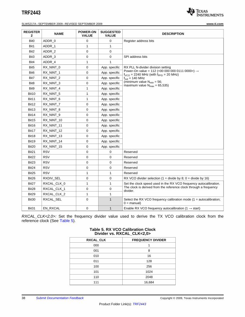
TRF2443
SLWS217A–SEPTEMBER 2009–REVISED SEPTEMBER 2009 ................................................................................................................................... www.ti.com
REGISTER POWER-ON SUGGESTEDNAME DESCRIPTION2 VALUE VALUEBit0 ADDR_0 0 0 Register address bitsBit1 ADDR_1 1 1Bit2 ADDR_2 0 0Bit3 ADDR_3 0 0 SPI address bitsBit4 ADDR_4 1 1Bit5 RX_NINT_0 0 App. specific RX PLL N-divider division setting
Power-On value = 112 (<00 000 000 0111 0000>) →Bit6 RX_NINT_1 0 App. specific fVCO = 2240 MHz (with fPFD = 20 MHz)Bit7 RX_NINT_2 0 App. specific fout = 140 MHz
(minimum value Nmin = 56;Bit8 RX_NINT_3 0 App. specificmaximum value Nmax = 65,535)
Bit9 RX_NINT_4 1 App. specificBit10 RX_NINT_5 1 App. specificBit11 RX_NINT_6 1 App. specificBit12 RX_NINT_7 0 App. specificBit13 RX_NINT_8 0 App. specificBit14 RX_NINT_9 0 App. specificBit15 RX_NINT_10 0 App. specificBit16 RX_NINT_11 0 App. specificBit17 RX_NINT_12 0 App. specificBit18 RX_NINT_13 0 App. specificBit19 RX_NINT_14 0 App. specificBit20 RX_NINT_15 0 App. specificBit21 RSV 0 0 ReservedBit22 RSV 0 0 ReservedBit23 RSV 0 0 ReservedBit24 RSV 0 0 ReservedBit25 RSV 1 1 ReservedBit26 RXDIV_SEL 0 0 RX VCO divider selection (1 = divide by 8; 0 = divide by 16)Bit27 RXCAL_CLK_0 1 1 Set the clock speed used in the RX VCO frequency autocalibration.
The clock is derived from the reference clock through a frequencyBit28 RXCAL_CLK_1 0 0 divider.Bit29 RXCAL_CLK_2 1 1Bit30 RXCAL_SEL 0 1 Select the RX VCO frequency calibration mode (1 = autocalibration;
0 = manual)Bit31 EN_RXCAL 0 1 Enable RX VCO frequency autocalibration (1 → start)
RXCAL_CLK<2,0>: Set the frequency divider value used to derive the TX VCO calibration clock from thereference clock (See Table 5).
Table 5. RX VCO Calibration ClockDivider vs. RXCAL_CLK<2,0>
RXCAL_CLK FREQUENCY DIVIDER000 1001 8010 16011 128100 256101 1024110 2048111 16,684
38 Submit Documentation Feedback Copyright © 2009, Texas Instruments Incorporated
Product Folder Link(s): TRF2443
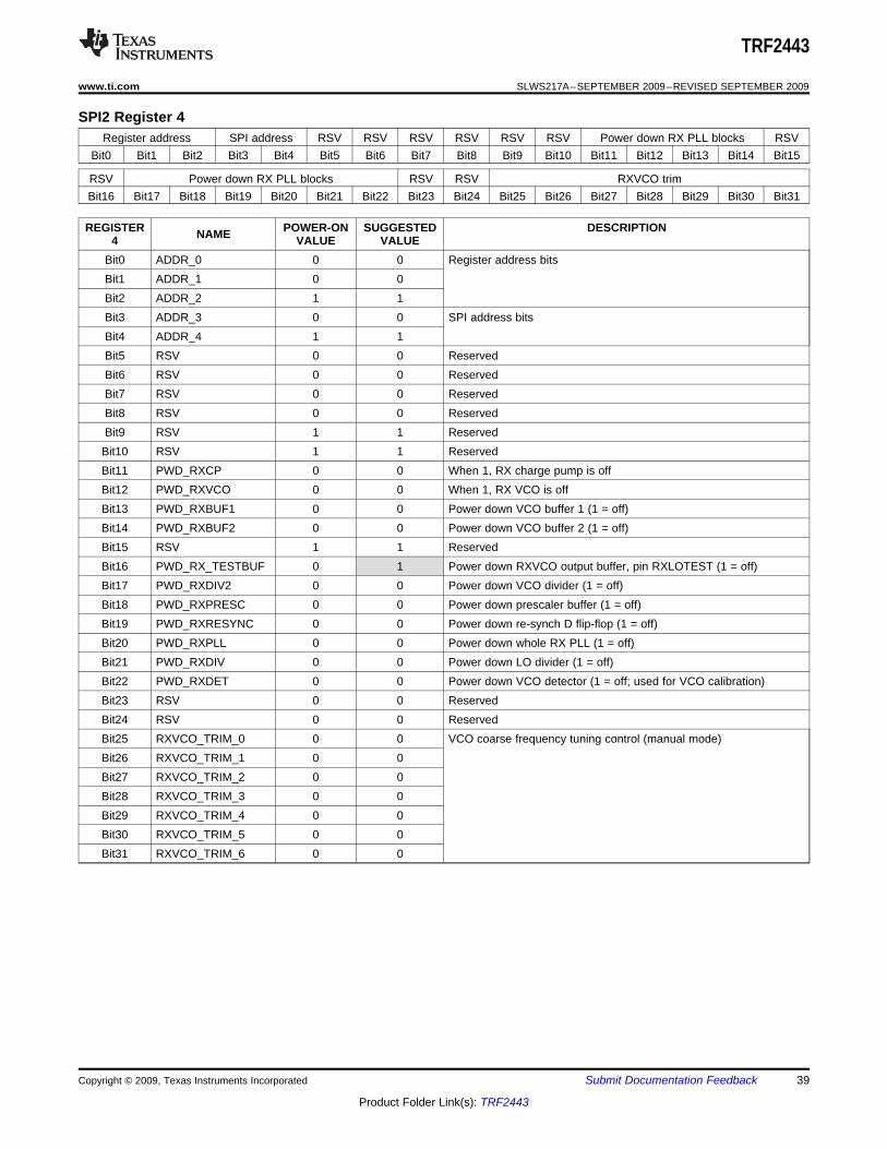
TRF2443
www.ti.com ................................................................................................................................... SLWS217A–SEPTEMBER 2009–REVISED SEPTEMBER 2009
SPI2 Register 4Register address SPI address RSV RSV RSV RSV RSV RSV Power down RX PLL blocks RSV
Bit0 Bit1 Bit2 Bit3 Bit4 Bit5 Bit6 Bit7 Bit8 Bit9 Bit10 Bit11 Bit12 Bit13 Bit14 Bit15
RSV Power down RX PLL blocks RSV RSV RXVCO trimBit16 Bit17 Bit18 Bit19 Bit20 Bit21 Bit22 Bit23 Bit24 Bit25 Bit26 Bit27 Bit28 Bit29 Bit30 Bit31
REGISTER POWER-ON SUGGESTED DESCRIPTIONNAME4 VALUE VALUEBit0 ADDR_0 0 0 Register address bitsBit1 ADDR_1 0 0Bit2 ADDR_2 1 1Bit3 ADDR_3 0 0 SPI address bitsBit4 ADDR_4 1 1Bit5 RSV 0 0 ReservedBit6 RSV 0 0 ReservedBit7 RSV 0 0 ReservedBit8 RSV 0 0 ReservedBit9 RSV 1 1 Reserved
Bit10 RSV 1 1 ReservedBit11 PWD_RXCP 0 0 When 1, RX charge pump is offBit12 PWD_RXVCO 0 0 When 1, RX VCO is offBit13 PWD_RXBUF1 0 0 Power down VCO buffer 1 (1 = off)Bit14 PWD_RXBUF2 0 0 Power down VCO buffer 2 (1 = off)Bit15 RSV 1 1 ReservedBit16 PWD_RX_TESTBUF 0 1 Power down RXVCO output buffer, pin RXLOTEST (1 = off)Bit17 PWD_RXDIV2 0 0 Power down VCO divider (1 = off)Bit18 PWD_RXPRESC 0 0 Power down prescaler buffer (1 = off)Bit19 PWD_RXRESYNC 0 0 Power down re-synch D flip-flop (1 = off)Bit20 PWD_RXPLL 0 0 Power down whole RX PLL (1 = off)Bit21 PWD_RXDIV 0 0 Power down LO divider (1 = off)Bit22 PWD_RXDET 0 0 Power down VCO detector (1 = off; used for VCO calibration)Bit23 RSV 0 0 ReservedBit24 RSV 0 0 ReservedBit25 RXVCO_TRIM_0 0 0 VCO coarse frequency tuning control (manual mode)Bit26 RXVCO_TRIM_1 0 0Bit27 RXVCO_TRIM_2 0 0Bit28 RXVCO_TRIM_3 0 0Bit29 RXVCO_TRIM_4 0 0Bit30 RXVCO_TRIM_5 0 0Bit31 RXVCO_TRIM_6 0 0
Copyright © 2009, Texas Instruments Incorporated Submit Documentation Feedback 39
Product Folder Link(s): TRF2443

TRF2443
SLWS217A–SEPTEMBER 2009–REVISED SEPTEMBER 2009 ................................................................................................................................... www.ti.com
SPI2 Register 5Register address SPI address RXPLL BIAS RSV RSV RXVCO BIAS BUF1 BIAS
Bit0 Bit1 Bit2 Bit3 Bit4 Bit5 Bit6 Bit7 Bit8 Bit9 Bit10 Bit11 Bit12 Bit13 Bit14 Bit15
BUF2 BIAS OUTBUF BIAS PRESC BIAS BIAS SEL VCO CAL REF RSV RSV RSV RSV RSV RSVBit16 Bit17 Bit18 Bit19 Bit20 Bit21 Bit22 Bit23 Bit24 Bit25 Bit26 Bit27 Bit28 Bit29 Bit30 Bit31
REGISTER POWER-ON SUGGESTEDNAME DESCRIPTION5 VALUE VALUEBit0 ADDR_0 1 1 Register address bitsBit1 ADDR_1 0 0Bit2 ADDR_2 1 1Bit3 ADDR_3 0 0 SPI address bitsBit4 ADDR_4 1 1Bit5 RXPLL_BIAS_0 0 0 RX PLL reference-current control bits. Adjust reference current from
40 µA to 60 µA.Bit6 RXPLL_BIAS_1 0 0Bit7 RXPLL_BIAS_2 1 1Bit8 RSV 0 0 ReservedBit9 RSV 0 0 Reserved
Bit10 RXVCO_BIAS_0 0 1 RX VCO bias-control bits. VCO current can be changed from 10 mA(0000) to 25 mA (1111), 1-mA steps.Bit11 RXVCO_BIAS_1 0 1
Bit12 RXVCO_BIAS_2 0 1Bit13 RXVCO_BIAS_3 1 1Bit14 RXBUF1_BIAS_0 0 0 It sets the PLL buffer 1 bias from 0.8 mA (00) to 2 mA (11), 0.4-mA
steps.Bit15 RXBUF1_BIAS_1 1 1Bit16 RXBUF2_BIAS_0 0 0 It sets the PLL buffer 2 bias from 0.8 mA (00) to 2 mA (11), 0.4-mA
steps.Bit17 RXBUF2_BIAS_1 1 1Bit18 RXBUFOUT_BIAS_0 0 0 RXPLL output-buffer reference bias current. 200 µA (00) to 500 µA
(11)Bit19 RXBUFOUT_BIAS_1 1 1Bit20 RXPRES_BIAS_0 1 0 RXPLL prescaler reference bias current. 200 µA (00) to 500 µA (11)Bit21 RXPRES_BIAS_1 1 1Bit22 RXVCO_CAL_IB 0 1 Select bias-current type for VCO calibration circuitry; 1 = PTAT; 0 =
constant over temperatureBit23 RXVCO_CAL_REF_0 0 1 RX VCO calibration reference voltage trimming.
000 → 1.175 VBit24 RXVCO_CAL_REF_1 0 1 111 → 2.05 V. Suggested value is 1.55 V (011).Bit25 RXVCO_CAL_REF_2 0 0Bit26 RSV 0 0 ReservedBit27 RSV 0 0 ReservedBit28 RSV 0 0 ReservedBit29 RSV 0 0 ReservedBit30 RSV 0 0 ReservedBit31 RSV 0 0 Reserved
40 Submit Documentation Feedback Copyright © 2009, Texas Instruments Incorporated
Product Folder Link(s): TRF2443
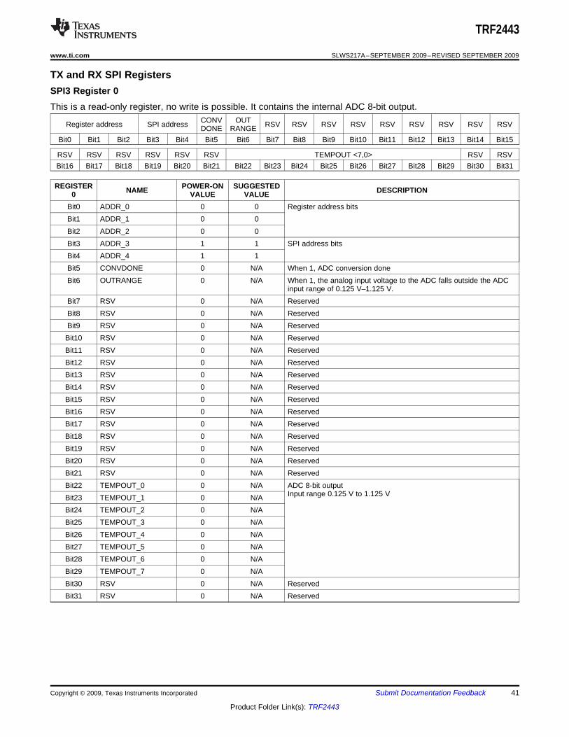
TX and RX SPI Registers
TRF2443
www.ti.com ................................................................................................................................... SLWS217A–SEPTEMBER 2009–REVISED SEPTEMBER 2009
SPI3 Register 0This is a read-only register, no write is possible. It contains the internal ADC 8-bit output.
CONV OUTRegister address SPI address RSV RSV RSV RSV RSV RSV RSV RSV RSVDONE RANGEBit0 Bit1 Bit2 Bit3 Bit4 Bit5 Bit6 Bit7 Bit8 Bit9 Bit10 Bit11 Bit12 Bit13 Bit14 Bit15
RSV RSV RSV RSV RSV RSV TEMPOUT <7,0> RSV RSVBit16 Bit17 Bit18 Bit19 Bit20 Bit21 Bit22 Bit23 Bit24 Bit25 Bit26 Bit27 Bit28 Bit29 Bit30 Bit31
REGISTER POWER-ON SUGGESTEDNAME DESCRIPTION0 VALUE VALUEBit0 ADDR_0 0 0 Register address bitsBit1 ADDR_1 0 0Bit2 ADDR_2 0 0Bit3 ADDR_3 1 1 SPI address bitsBit4 ADDR_4 1 1Bit5 CONVDONE 0 N/A When 1, ADC conversion doneBit6 OUTRANGE 0 N/A When 1, the analog input voltage to the ADC falls outside the ADC
input range of 0.125 V–1.125 V.Bit7 RSV 0 N/A ReservedBit8 RSV 0 N/A ReservedBit9 RSV 0 N/A Reserved
Bit10 RSV 0 N/A ReservedBit11 RSV 0 N/A ReservedBit12 RSV 0 N/A ReservedBit13 RSV 0 N/A ReservedBit14 RSV 0 N/A ReservedBit15 RSV 0 N/A ReservedBit16 RSV 0 N/A ReservedBit17 RSV 0 N/A ReservedBit18 RSV 0 N/A ReservedBit19 RSV 0 N/A ReservedBit20 RSV 0 N/A ReservedBit21 RSV 0 N/A ReservedBit22 TEMPOUT_0 0 N/A ADC 8-bit output
Input range 0.125 V to 1.125 VBit23 TEMPOUT_1 0 N/ABit24 TEMPOUT_2 0 N/ABit25 TEMPOUT_3 0 N/ABit26 TEMPOUT_4 0 N/ABit27 TEMPOUT_5 0 N/ABit28 TEMPOUT_6 0 N/ABit29 TEMPOUT_7 0 N/ABit30 RSV 0 N/A ReservedBit31 RSV 0 N/A Reserved
Copyright © 2009, Texas Instruments Incorporated Submit Documentation Feedback 41
Product Folder Link(s): TRF2443

TRF2443
SLWS217A–SEPTEMBER 2009–REVISED SEPTEMBER 2009 ................................................................................................................................... www.ti.com
SPI3 Register 1TX TX I and Q phaseRegister address SPI address TX VGA attenuation controlPWD unbalance correction
Bit0 Bit1 Bit2 Bit3 Bit4 Bit5 Bit6 Bit7 Bit8 Bit9 Bit10 Bit11 Bit12 Bit13 Bit14 Bit15
TX I and ... Enable Loopback Detect PD ref RSVcorrection loopback attenuator resetBit16 Bit17 Bit18 Bit19 Bit20 Bit21 Bit22 Bit23 Bit24 Bit25 Bit26 Bit27 Bit28 Bit29 Bit30 Bit31
REGISTER POWER-ON SUGGESTEDNAME DESCRIPTION1 VALUE VALUEBit0 ADDR_0 1 1 Register address bitsBit1 ADDR_1 0 0Bit2 ADDR_2 0 0Bit3 ADDR_3 1 1 SPI address bitsBit4 ADDR_4 1 1Bit5 PWD_TX 1 0 TX chain power down (1 = TX chain is off)Bit6 TX_ATT_0 0 App. specific TX chain variable-attenuator control;
000 0000 = minimum attenuation;Bit7 TX_ATT_1 0 App. specific 100 0111 = maximum attenuation (35.5 dB);Bit8 TX_ATT_2 0 App. specific attenuation step = 0.5 dB;Bit9 TX_ATT_3 1 App. specific
Bit10 TX_ATT_4 0 App. specificBit11 TX_ATT_5 0 App. specificBit12 TX_ATT_6 0 App. specificBit13 TXIQ_PHASE_0 0 0 TX LO I and Q phase-error correction bits. Suggested value is
(0 1000).Bit14 TXIQ_PHASE_1 0 0Bit15 TXIQ_PHASE_2 0 0Bit16 TXIQ_PHASE_3 0 1Bit17 TXIQ_PHASE_4 1 0Bit18 EN_LB 0 0 Enable loopback switch (1 = enable)Bit19 EN_LB_ATT 0 0 Enable 20-dB attenuator in loopback (1 = enable)Bit20 DET_RESET 0 0 Software reset of power-detect alarm outputBit21 PD_REF_BUF 0 0 Power down reference-frequency input buffer (1 = disable)Bit22 RSV 0 0 ReservedBit23 RSV 0 0 ReservedBit24 RSV 0 0 ReservedBit25 RSV 0 0 ReservedBit26 RSV 0 0 ReservedBit27 RSV 0 0 ReservedBit28 RSV 0 0 ReservedBit29 RSV 0 0 ReservedBit30 RSV 0 0 ReservedBit31 RSV 0 0 Reserved
PWD_TX (bit 5): When 1, the entire TX chain is off.
TX_ATT<6,0>: TX chain variable-attenuator control bits, 000 0000 corresponds to minimum attenuation(maximum gain), and 100 0111 sets the attenuator to maximum (minimum gain). The typical attenuation step is0.5 dB.
TXIQ_PHASE<4,0>: TX I-Q phase unbalance correction bits. These bits allow correcting ±2 degrees of phaseunbalance between the I and Q paths. Suggested value to program = 0 1000.
42 Submit Documentation Feedback Copyright © 2009, Texas Instruments Incorporated
Product Folder Link(s): TRF2443

TRF2443
www.ti.com ................................................................................................................................... SLWS217A–SEPTEMBER 2009–REVISED SEPTEMBER 2009
EN_LB (bit 18): When 1, the loopback switch, connecting the TX mixer output to the RX IFVGA3 input, is on.Also, when the switch is enabled, the TX amplifier, RX LNA, IFVGA1, and IFVGA2 are turned off (see theApplication Information section).
EN_LB_ATT (bit 19): When 1, a 20-dB attenuator in the loopback path is enabled (see the ApplicationInformation section).
DET_RESET (bit 20): Set this bit to 1 to reset the power-alarm output after it has gone low for a power-alarmalert (see the Application Information section).
SPI3 Register 2EnableRegister address SPI address RX LNA gain control RX baseband gainext SAW
Bit0 Bit1 Bit2 Bit3 Bit4 Bit5 Bit6 Bit7 Bit8 Bit9 Bit10 Bit11 Bit12 Bit13 Bit14 Bit15
BasebandFilter PWD PWDRX baseband-filter corner frequency 3-dB XPIC baseband gainbypass RX XPICattenuationBit16 Bit17 Bit18 Bit19 Bit20 Bit21 Bit22 Bit23 Bit24 Bit25 Bit26 Bit27 Bit28 Bit29 Bit30 Bit31
REGISTER POWER-ON SUGGESTED DESCRIPTIONNAME2 VALUE VALUEBit0 ADDR_0 0 0 Register address bitsBit1 ADDR_1 1 1Bit2 ADDR_2 0 0Bit3 ADDR_3 1 1 SPI address bitsBit4 ADDR_4 1 1Bit5 LNA_ATT_0 0 App. specific RX LNA attenuation control bits
<0 0000> corresponds to 0-dB attenuation (maximum gain).Bit6 LNA_ATT_1 0 App. specific<1 0011> corresponds to 19-dB attenuation (minimum gain).
Bit7 LNA_ATT_2 0 App. specific Gain step is 1 dB.Bit8 LNA_ATT_3 0 App. specificBit9 LNA_ATT_4 0 App. specific
Bit10 EN_SAW 0 App. specific 1 = signal path through external SAW filter enabledBit11 RXBB_GAIN_0 0 App. specific RX baseband amplifier gain setting
<1 1000> = maximum gain (33 dB); gain step is 1 dB.Bit12 RXBB_GAIN_1 0 App. specificRXBB_GAIN<4,0> = wanted gain – 9
Bit13 RXBB_GAIN_2 0 App. specific Example: wanted gain = 22 dB → New gain setting = 22 – 9 = 13 =Bit14 RXBB_GAIN_3 0 App. specific <0 1101>Bit15 RXBB_GAIN_4 1 App. specificBit16 RXBB_FREQ_0 0 App. specific RX baseband-filter cutoff-frequency setting
Setting of <111 1111> corresponds to minimum cutoff frequency.Bit17 RXBB_FREQ_1 1 App. specificSee the Baseband-Filter Cutoff-Frequency Calibration section.
Bit18 RXBB_FREQ_2 1 App. specificBit19 RXBB_FREQ_3 1 App. specificBit20 RXBB_FREQ_4 1 App. specificBit21 RXBB_FREQ_5 0 App. specificBit22 RXBB_FREQ_6 1 App. specificBit23 RXBB_FLT_BYP 0 App. specific RX baseband filter bypassBit24 RXBB_3dBATT 1 App. specific Enable 3-dB attenuator in the RX BB output buffer (1 = on)Bit25 PWD_RX 0 0 Power down receiver chainBit26 PWD_XPIC 0 0 Power down XPICBit27 XPICBB_GAIN_0 0 App. specific XPIC baseband-amplifier gain setting. <xxx> = maximum gain (xx
dB); gain step is 1 dB.Bit28 XPICBB_GAIN_1 1 App. specificXPICBB_GAIN<4,0> = wanted gain – 9
Bit29 XPICBB_GAIN_2 1 App. specific Example: wanted gain = 12 dB → New gain setting = 12 – 9 = 3 =<0 0011>Bit30 XPICBB_GAIN_3 0 App. specific
Bit31 XPICBB_GAIN_4 0 App. specific
Copyright © 2009, Texas Instruments Incorporated Submit Documentation Feedback 43
Product Folder Link(s): TRF2443
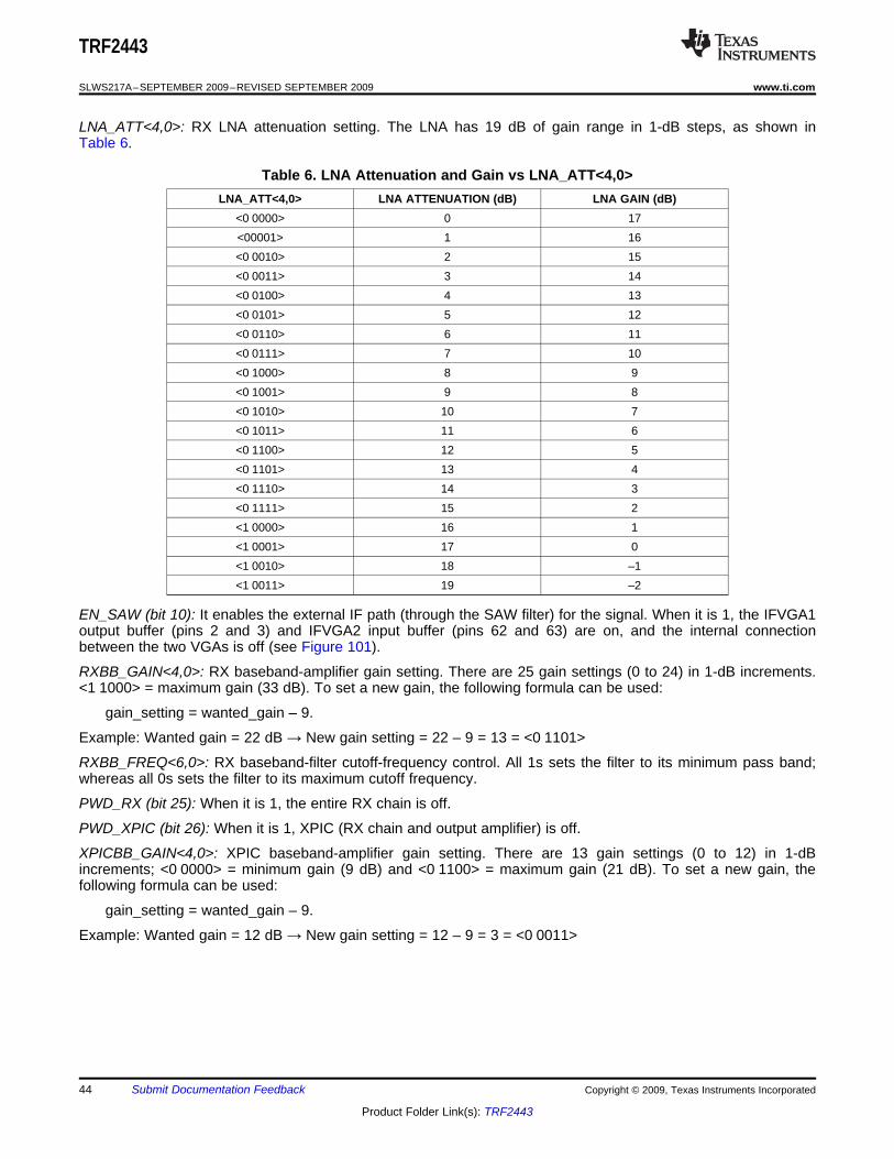
TRF2443
SLWS217A–SEPTEMBER 2009–REVISED SEPTEMBER 2009 ................................................................................................................................... www.ti.com
LNA_ATT<4,0>: RX LNA attenuation setting. The LNA has 19 dB of gain range in 1-dB steps, as shown inTable 6.
Table 6. LNA Attenuation and Gain vs LNA_ATT<4,0>LNA_ATT<4,0> LNA ATTENUATION (dB) LNA GAIN (dB)
<0 0000> 0 17<00001> 1 16<0 0010> 2 15<0 0011> 3 14<0 0100> 4 13<0 0101> 5 12<0 0110> 6 11<0 0111> 7 10<0 1000> 8 9<0 1001> 9 8<0 1010> 10 7<0 1011> 11 6<0 1100> 12 5<0 1101> 13 4<0 1110> 14 3<0 1111> 15 2<1 0000> 16 1<1 0001> 17 0<1 0010> 18 –1<1 0011> 19 –2
EN_SAW (bit 10): It enables the external IF path (through the SAW filter) for the signal. When it is 1, the IFVGA1output buffer (pins 2 and 3) and IFVGA2 input buffer (pins 62 and 63) are on, and the internal connectionbetween the two VGAs is off (see Figure 101).
RXBB_GAIN<4,0>: RX baseband-amplifier gain setting. There are 25 gain settings (0 to 24) in 1-dB increments.<1 1000> = maximum gain (33 dB). To set a new gain, the following formula can be used:
gain_setting = wanted_gain – 9.
Example: Wanted gain = 22 dB → New gain setting = 22 – 9 = 13 = <0 1101>
RXBB_FREQ<6,0>: RX baseband-filter cutoff-frequency control. All 1s sets the filter to its minimum pass band;whereas all 0s sets the filter to its maximum cutoff frequency.
PWD_RX (bit 25): When it is 1, the entire RX chain is off.
PWD_XPIC (bit 26): When it is 1, XPIC (RX chain and output amplifier) is off.
XPICBB_GAIN<4,0>: XPIC baseband-amplifier gain setting. There are 13 gain settings (0 to 12) in 1-dBincrements; <0 0000> = minimum gain (9 dB) and <0 1100> = maximum gain (21 dB). To set a new gain, thefollowing formula can be used:
gain_setting = wanted_gain – 9.
Example: Wanted gain = 12 dB → New gain setting = 12 – 9 = 3 = <0 0011>
44 Submit Documentation Feedback Copyright © 2009, Texas Instruments Incorporated
Product Folder Link(s): TRF2443
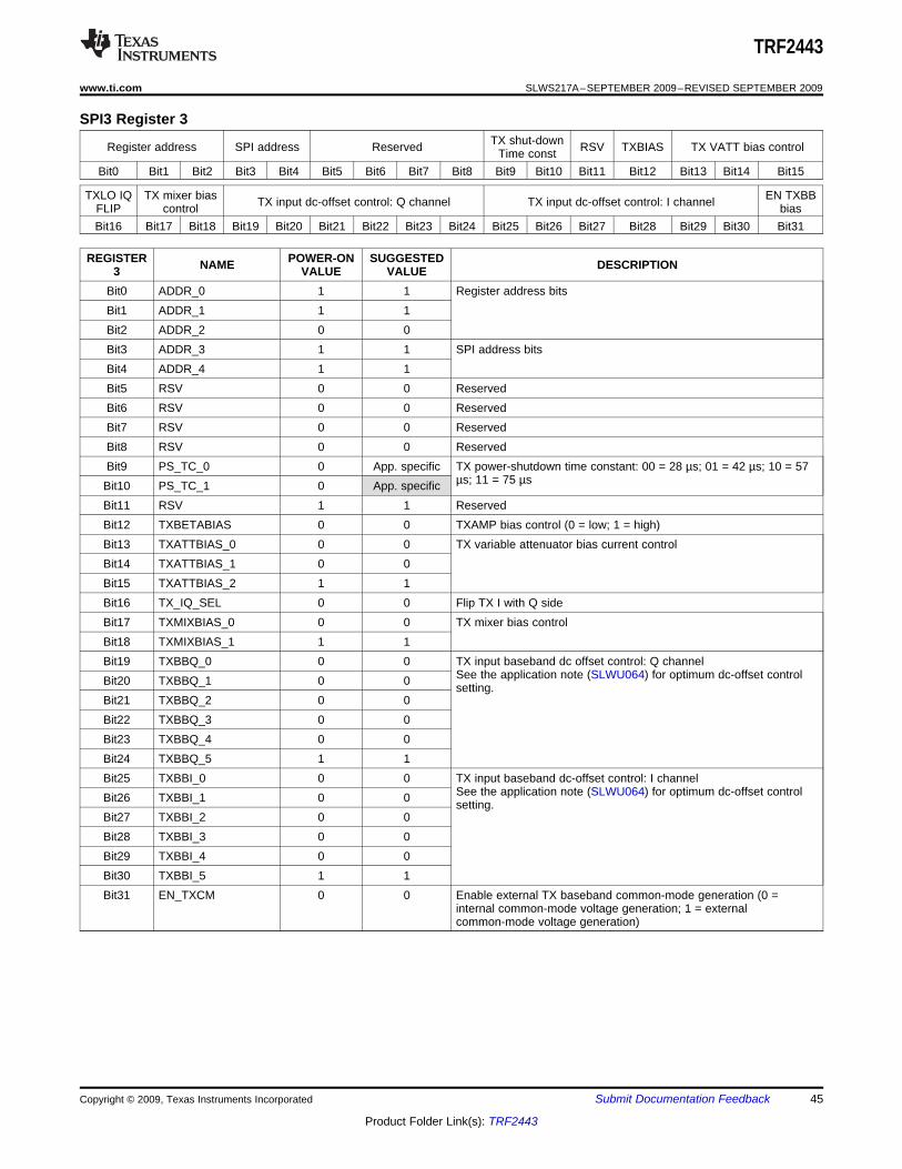
TRF2443
www.ti.com ................................................................................................................................... SLWS217A–SEPTEMBER 2009–REVISED SEPTEMBER 2009
SPI3 Register 3TX shut-downRegister address SPI address Reserved RSV TXBIAS TX VATT bias controlTime const
Bit0 Bit1 Bit2 Bit3 Bit4 Bit5 Bit6 Bit7 Bit8 Bit9 Bit10 Bit11 Bit12 Bit13 Bit14 Bit15
TXLO IQ TX mixer bias EN TXBBTX input dc-offset control: Q channel TX input dc-offset control: I channelFLIP control biasBit16 Bit17 Bit18 Bit19 Bit20 Bit21 Bit22 Bit23 Bit24 Bit25 Bit26 Bit27 Bit28 Bit29 Bit30 Bit31
REGISTER POWER-ON SUGGESTEDNAME DESCRIPTION3 VALUE VALUEBit0 ADDR_0 1 1 Register address bitsBit1 ADDR_1 1 1Bit2 ADDR_2 0 0Bit3 ADDR_3 1 1 SPI address bitsBit4 ADDR_4 1 1Bit5 RSV 0 0 ReservedBit6 RSV 0 0 ReservedBit7 RSV 0 0 ReservedBit8 RSV 0 0 ReservedBit9 PS_TC_0 0 App. specific TX power-shutdown time constant: 00 = 28 µs; 01 = 42 µs; 10 = 57
µs; 11 = 75 µsBit10 PS_TC_1 0 App. specificBit11 RSV 1 1 ReservedBit12 TXBETABIAS 0 0 TXAMP bias control (0 = low; 1 = high)Bit13 TXATTBIAS_0 0 0 TX variable attenuator bias current controlBit14 TXATTBIAS_1 0 0Bit15 TXATTBIAS_2 1 1Bit16 TX_IQ_SEL 0 0 Flip TX I with Q sideBit17 TXMIXBIAS_0 0 0 TX mixer bias controlBit18 TXMIXBIAS_1 1 1Bit19 TXBBQ_0 0 0 TX input baseband dc offset control: Q channel
See the application note (SLWU064) for optimum dc-offset controlBit20 TXBBQ_1 0 0 setting.Bit21 TXBBQ_2 0 0Bit22 TXBBQ_3 0 0Bit23 TXBBQ_4 0 0Bit24 TXBBQ_5 1 1Bit25 TXBBI_0 0 0 TX input baseband dc-offset control: I channel
See the application note (SLWU064) for optimum dc-offset controlBit26 TXBBI_1 0 0 setting.Bit27 TXBBI_2 0 0Bit28 TXBBI_3 0 0Bit29 TXBBI_4 0 0Bit30 TXBBI_5 1 1Bit31 EN_TXCM 0 0 Enable external TX baseband common-mode generation (0 =
internal common-mode voltage generation; 1 = externalcommon-mode voltage generation)
Copyright © 2009, Texas Instruments Incorporated Submit Documentation Feedback 45
Product Folder Link(s): TRF2443
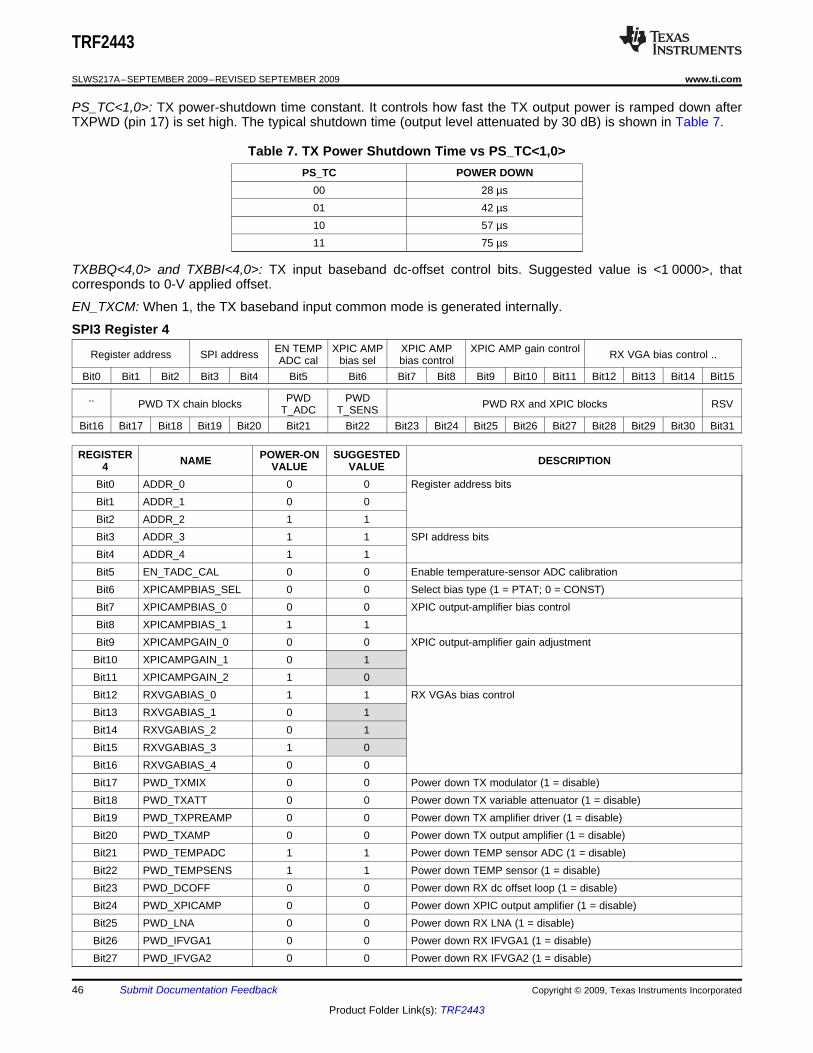
TRF2443
SLWS217A–SEPTEMBER 2009–REVISED SEPTEMBER 2009 ................................................................................................................................... www.ti.com
PS_TC<1,0>: TX power-shutdown time constant. It controls how fast the TX output power is ramped down afterTXPWD (pin 17) is set high. The typical shutdown time (output level attenuated by 30 dB) is shown in Table 7.
Table 7. TX Power Shutdown Time vs PS_TC<1,0>PS_TC POWER DOWN
00 28 µs01 42 µs10 57 µs11 75 µs
TXBBQ<4,0> and TXBBI<4,0>: TX input baseband dc-offset control bits. Suggested value is <1 0000>, thatcorresponds to 0-V applied offset.
EN_TXCM: When 1, the TX baseband input common mode is generated internally.
SPI3 Register 4EN TEMP XPIC AMP XPIC AMP XPIC AMP gain controlRegister address SPI address RX VGA bias control ..ADC cal bias sel bias control
Bit0 Bit1 Bit2 Bit3 Bit4 Bit5 Bit6 Bit7 Bit8 Bit9 Bit10 Bit11 Bit12 Bit13 Bit14 Bit15
.. PWD PWDPWD TX chain blocks PWD RX and XPIC blocks RSVT_ADC T_SENSBit16 Bit17 Bit18 Bit19 Bit20 Bit21 Bit22 Bit23 Bit24 Bit25 Bit26 Bit27 Bit28 Bit29 Bit30 Bit31
REGISTER POWER-ON SUGGESTEDNAME DESCRIPTION4 VALUE VALUEBit0 ADDR_0 0 0 Register address bitsBit1 ADDR_1 0 0Bit2 ADDR_2 1 1Bit3 ADDR_3 1 1 SPI address bitsBit4 ADDR_4 1 1Bit5 EN_TADC_CAL 0 0 Enable temperature-sensor ADC calibrationBit6 XPICAMPBIAS_SEL 0 0 Select bias type (1 = PTAT; 0 = CONST)Bit7 XPICAMPBIAS_0 0 0 XPIC output-amplifier bias controlBit8 XPICAMPBIAS_1 1 1Bit9 XPICAMPGAIN_0 0 0 XPIC output-amplifier gain adjustment
Bit10 XPICAMPGAIN_1 0 1Bit11 XPICAMPGAIN_2 1 0Bit12 RXVGABIAS_0 1 1 RX VGAs bias controlBit13 RXVGABIAS_1 0 1Bit14 RXVGABIAS_2 0 1Bit15 RXVGABIAS_3 1 0Bit16 RXVGABIAS_4 0 0Bit17 PWD_TXMIX 0 0 Power down TX modulator (1 = disable)Bit18 PWD_TXATT 0 0 Power down TX variable attenuator (1 = disable)Bit19 PWD_TXPREAMP 0 0 Power down TX amplifier driver (1 = disable)Bit20 PWD_TXAMP 0 0 Power down TX output amplifier (1 = disable)Bit21 PWD_TEMPADC 1 1 Power down TEMP sensor ADC (1 = disable)Bit22 PWD_TEMPSENS 1 1 Power down TEMP sensor (1 = disable)Bit23 PWD_DCOFF 0 0 Power down RX dc offset loop (1 = disable)Bit24 PWD_XPICAMP 0 0 Power down XPIC output amplifier (1 = disable)Bit25 PWD_LNA 0 0 Power down RX LNA (1 = disable)Bit26 PWD_IFVGA1 0 0 Power down RX IFVGA1 (1 = disable)Bit27 PWD_IFVGA2 0 0 Power down RX IFVGA2 (1 = disable)
46 Submit Documentation Feedback Copyright © 2009, Texas Instruments Incorporated
Product Folder Link(s): TRF2443

TRF2443
www.ti.com ................................................................................................................................... SLWS217A–SEPTEMBER 2009–REVISED SEPTEMBER 2009
REGISTER POWER-ON SUGGESTEDNAME DESCRIPTION4 VALUE VALUEBit28 PWD_IFVGA3 0 0 Power down RX IFVGA3 (1 = disable)Bit29 PWD_RXMIX 0 0 Power down RX demodulator (1 = disable)Bit30 PWD_RXBB 0 0 Power down RX baseband (1 = disable)Bit31 RSV 0 0 Reserved
EN_TADC_CAL (bit 5): When 1, TEMP sensor ADC autocalibration starts.
XPICAMPBIAS_SEL (bit 6): It selects the XPIC output amplifier biasing type. When 1, a PTAT (proportional totemperature) dc current is selected. If it is 0, then a constant current over temperature is chosen.
SPI3 Register 5ENBB DC offset DC offset CLKRegister address SPI address RXMIX BIAS RX IMIX VCM RXQMIX VCMAUTOCAL resolution
Bit0 Bit1 Bit2 Bit3 Bit4 Bit5 Bit6 Bit7 Bit8 Bit9 Bit10 Bit11 Bit12 Bit13 Bit14 Bit15
ENXPIC XPIC MIX XPIC IMIX XPIC QMIX XPIC dc offset PWD dc... RSV XPIC dc offset CLK RSVCAL BIAS VCM VCM resolution OFFBit16 Bit17 Bit18 Bit19 Bit20 Bit21 Bit22 Bit23 Bit24 Bit25 Bit26 Bit27 Bit28 Bit29 Bit30 Bit31
REGISTER NAME POWER-ON SUGGESTED DESCRIPTION5 VALUE VALUE
Bit0 ADDR_0 1 1 Register address bitsBit1 ADDR_1 0 0Bit2 ADDR_2 1 1Bit3 ADDR_3 1 1 SPI address bitsBit4 ADDR_4 1 1Bit5 EN_BB_AUTOCAL 0 0 Enable RX baseband dc-offset autocalibrationBit6 RXMIX_BIAS_0 1 1 RX demodulator dc current controlBit7 RXMIX_BIAS_1 0 0Bit8 RXIMIX_VCM_0 0 0 RX I mixer bias controlBit9 RXIMIX_VCM_1 1 1
Bit10 RXQMIX_VCM_0 0 0 RX Q mixer bias controlBit11 RXQMIX_VCM_1 1 1Bit12 DCOFF_BIAS_0 1 1 Set RX dc-offset calibration-loop resolutionBit13 DCOFF_BIAS_1 1 1Bit14 DCOFF_CLK_0 0 0 RX dc offset-loop clock-speed controlBit15 DCOFF_CLK_1 0 0Bit16 DCOFF_CLK_2 1 1Bit17 RSV 0 0 ReservedBit18 EN_XPIC_AUTOCAL 0 0 Enable XPIC baseband dc-offset autocalibrationBit19 XMIX_BIAS_0 1 0 XPIC demodulator dc-current controlBit20 XMIX_BIAS_1 0 1Bit21 XIMIX_VCM_0 0 0 XPIC I mixer bias controlBit22 XIMIX_VCM_1 1 1Bit23 XQMIX_VCM_0 0 0 XPIC Q mixer bias controlBit24 XQMIX_VCM_1 1 1Bit25 XPICDCOFF_BIAS_0 1 1 Set XPIC dc-offset calibration-loop resolutionBit26 XPICDCOFF_BIAS_1 1 1Bit27 XDCOFF_CLK_0 0 0 XPIC dc offset-loop clock-speed controlBit28 XDCOFF_CLK_1 0 0Bit29 XDCOFF_CLK_2 1 1Bit30 RSV 1 1 Reserved
Copyright © 2009, Texas Instruments Incorporated Submit Documentation Feedback 47
Product Folder Link(s): TRF2443

TRF2443
SLWS217A–SEPTEMBER 2009–REVISED SEPTEMBER 2009 ................................................................................................................................... www.ti.com
REGISTER NAME POWER-ON SUGGESTED DESCRIPTION5 VALUE VALUE
Bit31 PWD_XPICDCOFF 0 0 Power down XPIC dc-offset loop (1 = disable)
EN_BB_AUTOCAL (bit5): When 1, the RX baseband dc-offset automatic calibration starts. At the end of thecalibration, the bit is reset to 0.
DCOFF_BIAS<2,0>: These bits control the maximum output dc voltage of the dc-offset correction DAC used inthe RX chain.
DCOFF_CLK<2,0>: It sets the frequency-divider ratio that creates the RX dc-offset correction-loop clock from theclock divider.
EN_BB_CAL (bit17): When 1, the RX baseband dc-offset loop is enabled.
EN_XPIC_AUTOCAL (bit18): When 1, the XPIC baseband dc-offset automatic calibration starts. At the end ofthe calibration, the bit is reset to 0.
XPICDCOFF_BIAS<2,0>: These bits control the maximum output dc voltage of the dc-offset correction DACused in the XPIC chain.
XDCOFF_CLK<2,0>: It sets the frequency-divider ratio that creates the XPIC dc-offset correction-loop clock fromthe clock divider.
SPI3 Register 6IFVGA2 gain-Register address SPI address IFVGA3 gain-range control IFVGA3 min. gain range control
Bit0 Bit1 Bit2 Bit3 Bit4 Bit5 Bit6 Bit7 Bit8 Bit9 Bit10 Bit11 Bit12 Bit13 Bit14 Bit15
IFVGA2 gain-range IFVGA2 min. gain IFVGA1 gain-range control IFVGA1 min. gaincontrolBit16 Bit17 Bit18 Bit19 Bit20 Bit21 Bit22 Bit23 Bit24 Bit25 Bit26 Bit27 Bit28 Bit29 Bit30 Bit31
REGISTER POWER-ON SUGGESTEDNAME DESCRIPTION6 VALUE VALUEBit0 ADDR_0 0 0 Register address bitsBit1 ADDR_1 1 1Bit2 ADDR_2 1 1Bit3 ADDR_3 1 1 SPI address bitsBit4 ADDR_4 1 1Bit5 IFVGA3_RANGE_0 0 0 IFVGA3 gain-range controlBit6 IFVGA3_RANGE_1 0 1Bit7 IFVGA3_RANGE_2 1 0Bit8 IFVGA3_RANGE_3 1 1Bit9 IFVGA3_RANGE_4 1 0
Bit10 IFVGA3_ MINGAIN_0 0 0 IFVGA3 minimum-gain controlBit11 IFVGA3_MINGAIN_1 1 1Bit12 IFVGA3_MINGAIN_2 0 0Bit13 IFVGA3_MINGAIN_3 0 0Bit14 IFVGA2_RANGE_0 0 1 IFVGA2 gain-range controlBit15 IFVGA2_RANGE_1 0 0Bit16 IFVGA2_RANGE_2 1 0Bit17 IFVGA2_RANGE_3 1 1Bit18 IFVGA2_RANGE_4 1 0Bit19 IFVGA2_ MINGAIN_0 0 0 IFVGA2 minimum-gain controlBit20 IFVGA2_MINGAIN_1 1 1Bit21 IFVGA2_MINGAIN_2 0 0Bit22 IFVGA2_MINGAIN_3 0 0
48 Submit Documentation Feedback Copyright © 2009, Texas Instruments Incorporated
Product Folder Link(s): TRF2443

TRF2443
www.ti.com ................................................................................................................................... SLWS217A–SEPTEMBER 2009–REVISED SEPTEMBER 2009
REGISTER POWER-ON SUGGESTEDNAME DESCRIPTION6 VALUE VALUEBit23 IFVGA1_RANGE_0 0 0 IFVGA1 gain-range controlBit24 IFVGA1_RANGE_1 0 0Bit25 IFVGA1_RANGE_2 1 1Bit26 IFVGA1_RANGE_3 1 1Bit27 IFVGA1_RANGE_4 1 1Bit28 IFVGA1_ MINGAIN_0 0 0 IFVGA1 minimum-gain controlBit29 IFVGA1_MINGAIN_1 1 0Bit30 IFVGA1_MINGAIN_2 0 1Bit31 IFVGA1_MINGAIN_3 0 0
Copyright © 2009, Texas Instruments Incorporated Submit Documentation Feedback 49
Product Folder Link(s): TRF2443

TRF2443
SLWS217A–SEPTEMBER 2009–REVISED SEPTEMBER 2009 ................................................................................................................................... www.ti.com
SPI3 Register 7Register address SPI address RX BB I dc offset DAC RX BB Q dc offset DAC
Bit0 Bit1 Bit2 Bit3 Bit4 Bit5 Bit6 Bit7 Bit8 Bit9 Bit10 Bit11 Bit12 Bit13 Bit14 Bit15
CAL PWD DET PWR DETECTORRX BB Q dc offset DAC RSV RSV RSV RSV RSVSEL DELAY THRESHOLDBit16 Bit17 Bit18 Bit19 Bit20 Bit21 Bit22 Bit23 Bit24 Bit25 Bit26 Bit27 Bit28 Bit29 Bit30 Bit31
REGISTER POWER-ON SUGGESTEDNAME DESCRIPTION7 VALUE VALUEBit0 ADDR_0 1 1 Register address bitsBit1 ADDR_1 1 1Bit2 ADDR_2 1 1Bit3 ADDR_3 1 1 SPI address bitsBit4 ADDR_4 1 1Bit5 RXBBI_DCOFF_0 0 0 RX baseband I-side dc-offset control DACBit6 RXBBI_DCOFF_1 0 0Bit7 RXBBI_DCOFF_2 0 0Bit8 RXBBI_DCOFF_3 0 0Bit9 RXBBI_DCOFF_4 0 0
Bit10 RXBBI_DCOFF_5 0 0Bit11 RXBBI_DCOFF_6 0 0Bit12 RXBBI_DCOFF_7 1 1Bit13 RXBBQ_DCOFF_0 0 0 RX baseband Q-side dc-offset control DACBit14 RXBBQ_DCOFF_1 0 0Bit15 RXBBQ_DCOFF_2 0 0Bit16 RXBBQ_DCOFF_3 0 0Bit17 RXBBQ_DCOFF_4 0 0Bit18 RXBBQ_DCOFF_5 0 0Bit19 RXBBQ_DCOFF_6 0 0Bit20 RXBBQ_DCOFF_7 1 1Bit21 RXBB_CALSELECT 1 1 RX baseband dc-offset calibration select (1 = automatic; 0 = manual)Bit22 PWRDET_DEL_0 1 App. Specific Power-detector-response delay controlBit23 PWRDET_DEL_1 0 App. SpecificBit25 PWRDET_0 0 0Bit25 PWRDET_1 0 1 TX power-detector threshold settingBit26 PWRDET_2 0 0Bit27 RSV 0 0 ReservedBit28 RSV 0 0 ReservedBit29 RSV 0 0 ReservedBit30 RSV 0 0 ReservedBit31 RSV 0 0 Reserved
RXBBI_DCOFF<7,0> and RXBBI_DCOFF<7,0>: TRF2443 internal auxiliary DAC bits to be set during themanual RX-chain baseband dc-offset calibration (see the Application Information section).
RXBB_CALSELECT (bit 21): Selects the dc-offset calibration mode; when 0, the manual mode is selected.
PWRDET_DEL<1,0>: TX power-detector response-time delay (see Table 8).
50 Submit Documentation Feedback Copyright © 2009, Texas Instruments Incorporated
Product Folder Link(s): TRF2443
READBACK MODE
32nd
Write
clock
pulse
1st Read
clock pulse2nd Read
clock pulse
32nd Read
clock pulse
33rd Read
clock pulse
“End of Write Cycle”
pulse
ReadBack
Data Bit31
Read
Back
Data
Bit1
Read
Back
Data
Bit29
ReadBack
Data Bit30ReadBack
Data Bit0
CLOCK
READBACK
DATA
RE
AD
BA
CK
td
tsu2 t
w
LATCH
ENABLE
1st Write
clock
pulse
tsu1
th t
(CLK)
32nd
Writes
clock
pulse
DB2
Address Bit2
DB1
Address Bit1
CLOCK
DATA
t(CL)
t(CH)
LATCH
ENABLE
DB3
Address Bit3
RE
GIS
TE
RW
RIT
E
tw
tsu2
tsu3
DB0 (LSB)
Address Bit0 DB29 DB30 DB31 (MSB)
TRF2443
www.ti.com ................................................................................................................................... SLWS217A–SEPTEMBER 2009–REVISED SEPTEMBER 2009
Table 8. TX Power-Detector Response-Time Delay vsPWRDET_DEL<1,0>
PWRDET_DEL DET DELAY00 5 µs01 10 µs10 20 µs11 40 µs
PWRDET<2,0>: TX power-detector threshold-level control
The TRF2443 implements the capability to read back the content of the serial programming-interface registers.Each readback is composed of two phases:1. Writing a request to read back data2. Reading the actual data of the internal registers (see timing diagram in Figure 100).
During the writing phase, a command is sent to the TRF2443 to set it in readback mode and to specify whichregister is to be read. In the proper reading phase, at each rising clock edge, the internal data is transferred tothe RDBKSPI pin and can be read at the following falling edge (LSB first). The first clock after the LE goes high(end of writing cycle) is idle, and the following 32 clock pulses transfer the internal register content to theRDBKSPI pin.
Figure 100. SPI Readback Timing Diagram
Copyright © 2009, Texas Instruments Incorporated Submit Documentation Feedback 51
Product Folder Link(s): TRF2443
Readback From the Internal Register Banks
TRF2443
SLWS217A–SEPTEMBER 2009–REVISED SEPTEMBER 2009 ................................................................................................................................... www.ti.com
Table 9. SPI Readback TimingPARAMETER MIN TYP MAX UNITS COMMENTS
th Hold time, data to clock 20 nstSU1 Setup time, data to clock 20 nst(CL) Clock low duration 20 nst(CH) Clock high duration 20 nstSU2 Setup time, clock to enable 20 nstW Enable time 50 ns Equals clock periodt(CLK) Clock period 50 nstSU3 Setup time, latch to data 70 nstd Delay time, clock to readback-data output 10 ns
The TX PLL (SPI-1) and RX PLL (SPI-2) register banks each contain six registers: register 0 (000) throughregister 5 (101). Register 0 (000) is used only for the readback operation, whereas registers 1 through 5 are theactual PLL control registers. In the case of the TX PLL (SPI-1) and RX PLL (SPI-2) register banks, register 0contains no information. Therefore, it is not possible to read back register 0 from these register banks.
The TX-RX (SPI-3) register bank contains eight registers: register 0 (000) through register 7 (111). Register 0(000) is used only for the readback operation, whereas registers 1 through 7 are the actual TX and RX controlregisters. In the case of the TX-RX register bank (SPI-3), register 0 is used to store some TRF2443 internal data.Therefore, it is possible to read back register 0 from this register bank, as it contains this data.
To read back a register from any of these register banks, register 0 of the register bank which contains theregister to be read must be programmed with a specific command that sets the TRF2443 in the readback modeand specifies the register to be read:• Set B<31> to 1 to put the TRF2443 in readback mode.• Set B<30,28> equal to the address of the register to be read (001 to 101 in the case of TX PLL/RX PLL; 000
to 111 in the case of TX-RX SPI).
52 Submit Documentation Feedback Copyright © 2009, Texas Instruments Incorporated
Product Folder Link(s): TRF2443

TRF2443
www.ti.com ................................................................................................................................... SLWS217A–SEPTEMBER 2009–REVISED SEPTEMBER 2009
Table 10. SPI Register Banks Readback SetupSUGGESTEDBITS NAME DESCRIPTIONVALUE
B0 ADDR <0> 0 Register 0 to be programmed to set TRF2443 in readback modeB1 ADDR <1> 0
Address bits B2 ADDR <2> 0B3 ADDR <3> X Register bank: B<4,3> from which a particular register is to be read back
TX PLL (01); RX PLL (10); TX-RX SPI (11)B4 ADDR <4> XB5 N/C 0B6 N/C 0B7 N/C 0B8 N/C 0B9 N/C 0B10 N/C 0B11 N/C 0B12 N/C 0B13 N/C 0B14 N/C 0B15 N/C 0B16 N/C 0B17 N/C 0
Data fieldB19 N/C 0B20 N/C 0B21 N/C 0B22 N/C 0B23 N/C 0B24 N/C 0B25 N/C 0B26 N/C 0B27 N/C 0B28 RB_REG<0> X Address of the register within the bank that is being read back;B29 RB_REG<1> X Reg 1(001) to Reg 5(101) in TX PLL/RX PLL;
Reg 0(000) to Reg 7(111) in TX-RX SPIB30 RB_REG<2> XB31 RB_Enable 1 1 → Put the device in readback mode
Copyright © 2009, Texas Instruments Incorporated Submit Documentation Feedback 53
Product Folder Link(s): TRF2443

TRF2443 DESCRIPTION
RECEIVER DESCRIPTION
0/90
RX VGA
LNA
From SPI
from RXPLL
AGCCNTL
IFVGA1 IFVGA2 IFVGA3
From SPI
BB AMP/FLT
IF SAW
RX_IN
IF_OUT IF_IN
RX_BBI
RX_BBQ
RX_AGC
LNA
VGA
Demodulator
TRF2443
SLWS217A–SEPTEMBER 2009–REVISED SEPTEMBER 2009 ................................................................................................................................... www.ti.com
Figure 101. Receiver Chain Block Diagram
The TRF2443 features a highly linear low-noise receiver chain with over 60 dB of analog-controlled gain rangeand more than 40 dB of gain range programmable via the serial programming interface (SPI) in 1-dB steps.Moreover, the TRF2443 gives the flexibility to add an external IF filter to further remove unwanted signals. Suchan external filter can be bypassed using an internal path that can be enabled via SPI.
The first block of the receiver chain is a low-noise, highly linear IF amplifier (LNA). Its input is differential andinternally matched to 50 Ω. To drive the TRF2443 RX input via a single0-ended source, a 1:1 balun is required atthe LNA input (see Application Schematic section). The TRF2443 LNA attenuation is programmable via the serialprogramming interface (SPI) from 0 dB to –19 dB, corresponding to an LNA gain of 17 dB to –2 dB (1-dB steps).LNA_ATT<4,0> in SPI-3, register 2, B<9,5> are the LNA attenuation controlling bits. To program the amplifier tothe maximum gain, set the attenuation bits to 0 (LNA_ATT<4,0> = <0 0000>); whereas minimum gaincorresponds to LNA_ATT<4,0> = <1 0011>.
The LNA is followed by three analog-controlled VGAs that provide more than 60 dB of gain range. The IFVGA1output and IFVGA2 input can be connected externally (pins IFOUT and IFIN) through an external IF filter. TheIFVGA1 output buffer requires two pullup inductors to be connected from the IFOUTP/N pins to Vcc (seeApplication Schematic section). The IFVGA2 input (pins IFINN/P) is high-impedance. A 50-Ω external resistor isrequired across the IFINN and IFINP pins to provide a matching load to the IF filter output. An internal switchgives the flexibility to bypass the external filter. The internal bypass switch is controlled via the serialprogramming interface through bit EN_SAW (SPI-3, register 2, B<10>). By programming EN_SAW to 1, theexternal path is selected, whereas a 0 engages the internal bypass switch.
The VGA gain is controlled by the dc voltage applied to the RXAGC pin. By varying the input dc voltage from 0 Vto 2 V, the VGA total gain goes from minimum to maximum. The gain control is linear in dB, with a typical slopearound 51 dB/V. The RXAGC input provides a high input impedance, equivalent to a 100-kΩ resistance in serieswith a 4-pF capacitance.
The IFVGA3 drives the demodulator, which downconverts the IF input signal directly to baseband in phase andquadrature. The demodulator block includes the local oscillator in-phase and quadrature-generation circuitry,followed by the LO buffer. The LO chain also includes a frequency divider that can be programmed to divide by 8or 16. The frequency divider generates the RX LO from the RX VCO. By selecting a division ratio of 16, the RXLO can be set to 140 MHz (see the Programming the TRF2443 Synthesizers section).
54 Submit Documentation Feedback Copyright © 2009, Texas Instruments Incorporated
Product Folder Link(s): TRF2443

Baseband Section
TRANSMITTER DESCRIPTION
6
From SPI
0/90
To feedbackswitch
From TXPLL
TX_OUT
TXQ_IN
TXI_IN
Level
Detect
TX_PWD
ATTTXAMP
VCC
VCC
TX IQ Modulator
TRF2443
www.ti.com ................................................................................................................................... SLWS217A–SEPTEMBER 2009–REVISED SEPTEMBER 2009
The TRF2443 baseband section integrates a programmable gain amplifier (PGA) and programmable low-passfilter. The baseband PGA minimum gain is 9 dB, and the maximum gain is 33 dB. The PGA can be programmedin 25 gain settings (0 to 24) in 1-dB increments. Its gain can be changed by the RX_BBGAIN<4,0> bits (SPI-3,register 2, B<15,11> according to the following formula:
gain_setting = wanted_gain – 9.
Example: Wanted gain = 22 dB → New gain setting = 22 – 9 = 13 = <0 1101>
The TRF2443 baseband low-pass filter cutoff frequency can be programmed from 2 MHz to 11 MHz by settingappropriately the cutoff-frequency control bits RXBB_FREQ<6,0> (SPI-3, register 2, B<22,16>).RXBB_FREQ<6,0> = <111 1111> corresponds to the minimum corner frequency.
The baseband output buffers (ADC drivers) are designed to drive directly an analog-to-digital converter (ADC),either dc- or ac-coupled. The output common mode of the ADC drivers is set externally via the RXBBCM pin (pin40). When the TRF2443 is dc-connected to the ADC, the same dc common mode for both the ADC and theTRF2443 baseband output can be used.
Figure 102. Transmitter Chain Block Diagram
The transmitter chain integrates an IQ modulator followed by a variable attenuator and the final transmitteramplification stage. The last two blocks provide over 35 dB of gain range. A power-alarm circuit monitors thelevel at the modulator output, and its digital output goes low if the signal level falls below the user-specifiedthreshold level relative to the expected level.
The first block of the transmitter chain is the IQ modulator, which upconverts the incoming in-phase andquadrature signals to the TX IF frequency. The TRF2443 can be either ac- or dc-coupled to the digital-to-analogconverter (DAC). If a dc-coupled configuration is selected, then the modulator-input dc-common mode must beset externally to the appropriate level of 1.4 V and the common-mode bias generation must be set to externalmode via the SPI by setting EN_TXCM (SPI-3, register 3, B<31>) to 1. If an ac-coupled configuration is selected,then internal common-mode generation mode must be enabled via the SPI by setting EN_TXCM (SPI-3, register3, B<31>) to 0. When internal biasing is enabled, it is possible to apply a dc offset to either the I or Q side of theIQ modulator using the integrated dc DAC, accessible via the SPI (TXBBI<5,0>, SPI-3, register 3, B<30,25>;TXBBQ<5,0>, SPI-3, register 3, B<24,19>). An external 100 Ω differential resistor is required between the TXbaseband input pins (TXBBIP and TXBBIN, pins 22 and 21, and TXBBQP and TXBBQN, pins 20 and 19) ifutilizing the dc DAC. The optimum value of the dc DAC, which minimizes carrier leakage, can be read from theEEPROM within the TRF2443. See the application note (SLWU064) on how to access EEPROM information.The mixers of the IQ modulator use an external load. The collectors of the output transistors are connected to thepins MIXINDN and MIXINDP (pins 2 and 3). On the board, a pullup inductor to Vcc must be connected to each ofthose pins, as well as a shunt resistor between the pins (see the Application Schematic section).
Copyright © 2009, Texas Instruments Incorporated Submit Documentation Feedback 55
Product Folder Link(s): TRF2443

TX Variable Attenuator and Output Amplifier
SYNTHESIZERS DESCRIPTION
1/N2
PFD CP
Div-8/16
TXIFLO_I
TXIFLO_Q
From SPI
TXVCO
REF_CLKRXPLL_CPTXVCO
Tune
1/N1
PFDCP
Div-8/16
RXVCO
RXIFLO_I
RXIFLO_Q
RXVCO
Tune
R1 R2
Programming the TRF2443 Synthesizers
TRF2443
SLWS217A–SEPTEMBER 2009–REVISED SEPTEMBER 2009 ................................................................................................................................... www.ti.com
The IQ modulator drives a variable attenuator. This block provides 5.5 dB of total attenuation range in 0.5-dBsteps. The output amplifier integrates five attenuation steps of 6 dB each for total of 30 dB. The output amplifierin combination with the variable attenuator provides over 35.5 dB of monotonic output power control (0.5-dBsteps). The TRF2443 TX gain can be controlled via SPI TX_ATT<6,0> (SPI-3, register 1, B<12,6>).TX_ATT<6,0> sets the amount of attenuation in the variable attenuator and output amplifier.• TX_ATT<6,0> = 000 0000 → 0 dB attenuation (maximum gain)• TX_ATT<6,0> = 100 0111 → maximum attenuation (minimum gain)
The TX output amplifier uses an output open-collector arrangement. Therefore, each of the two output pins(TXOUTP and TXOUTN, pins 77 and 78) requires a pullup inductor connected to the power supply (see theApplication Schematic section). The TRF2443 TX output impedance is set typically to 200 Ω differential. A 4:1impedance-ratio balun is needed to transform the impedance to 50 Ω single-ended.
Figure 103. RX and TX PLL Block Diagram
The TRF2443 integrates two complete integer synthesizers for the receiver and transmitter chains. The RXVCOoperates at 16 times the typical RX input frequency, and the TXVCO operates at 8 times the typical TX outputfrequency.
Each synthesizer is composed of:• High-frequency VCO (around 2720 MHz for the TX VCO and 2240 MHz for the RX VCO)• N-divider (driven by the high-frequency VCO) done by an 8/9 prescaler followed by an A-B counter that drives
the phase-frequency detector• Phase-frequency detector (PFD) (driven by the N-divider) that compares the VCO divided by N to the
reference clock divided by R signals• Charge pump (driven by the PFD), which creates up and down current pulses based on the incoming signals
from the PFD. Its output is filtered and transformed to voltage by the external loop filter and applied to theVCO input control voltage.
• An external reference clock must be applied to REFIN (pin 16). The incoming signal is buffered and goesthrough a programmable divider (R-divider).
The VCO output is then routed through a programmable divider by 8 or 16 to create the TX and RX LO signals.The TRF2443 features a lock-detect output pin (LOCKDET, pin 5). This is a digital output that is high when bothRX and TX synthesizers are locked, and it is low if one or both synthesizers are unlocked (or lose lock).
Both TRF2443 synthesizers are integer PLLs. The VCO output frequency is defined by:fVCO = k × N / R × fRef
56 Submit Documentation Feedback Copyright © 2009, Texas Instruments Incorporated
Product Folder Link(s): TRF2443

Calibrating TRF2443 TX and RX VCO
Synthesizer Lock-Detector Indicator
TRF2443
www.ti.com ................................................................................................................................... SLWS217A–SEPTEMBER 2009–REVISED SEPTEMBER 2009
where:N: division ratio of the N-dividerR: division ratio of the R-dividerK: multiplier factor; k = 1 for RX synthesizer; k = 2 for the TX synthesizer.
Knowing the fRef, it is possible to calculate the required N and R values to synthesize any output frequency withinthe VCO frequency range.
ExampleSuppose we want to synthesize the TX LO to be 340 MHz and the input reference frequency is 20 MHz.
LOTX = 340 MHzfRef = 20 MHzfVCO-TX = 2720 MHz (8 × LOTX)
Because fVCO-TX is an integer multiple of fRef, we can set the R divider to 1.
R = 1N = fVCO-TX / (k × fRef) × R = 68
Then the TRF2443 SPI can be programmed as follows:
R = 1 → TXRDIV<13,0> = <00 0000 0000 0001> (SPI-1, register 1, B<18,5>)N = 68 → TX_NINT<15,0> = <0000 0000 0100 0100> (SPI-1, register 2, B<20,5>)LO divider set to 8 → TXDIV_SEL = 1 (SPI-1, register 2, B<26>).
Both TRF2443 VCOs are based on a cross-coupled LC tank architecture. The tank is composed of a high-Qintegrated spiral inductor, a varactor, and an array of capacitors which is digitally controlled. To tune the VCO toa certain frequency, the correct configuration for the array of capacitors is required. The capacitor array can beconfigured automatically or manually.
The calibration mode is controlled by TXCAL_SEL (SPI-1, register 2, B<30>) for the TX VCO and byRXCAL_SEL (SPI-2, register 2, B<30>) for the RX VCO. Setting these two bits to 1 selects the automaticcalibration mode. The calibration starts when EN_TXCAL (SPI-1, register 2, B<31>) and/or EN_RXCAL (SPI-2,register 2, B<31>) are toggled to 1. The calibration speed is controlled by a clock derived from the referenceclock through a frequency divider, whose division ratio can be programmed with TXCAL_CLK<2,0> (SPI-1,register 2, B<29,27>) and RXCAL_CLK<2,0> (SPI-2, register 2, B<29,27>). The suggested value ofTXCAL_CLK<2,0> and RXCAL_CLK<2,0> = <101>, which corresponds to a divider value of 1024 and a clockspeed of 20 MHz.
The manual-mode calibration, used mainly for debugging purposes, is activated by setting TXCAL_SEL (SPI-1,register 2, B<30>) and or RXCAL_SEL (SPI-2, register 2, B<30>) to 0. In this mode, the capacitor array setting iscontrolled by TXVCO_TRIM<5,0> (SPI-1, register 4, B<31,26>) for the TX VCO and RXVCO_TRIM<6,0> (SPI-2,register 4, B<31,26>) for the RX VCO.
The TRF2443 integrates a PLL lock-detector circuit. When both the TX and RX synthesizers are locked,LOCKDET (pin 5) goes high. The settling time of the lock-detector circuitry can be set externally by sizing thecapacitor placed between LDCAP (pin 38) and ground. The size of capacitor on this pin sets the time constantTld of the lock detect circuit. If either the TX PLL or the RX PLL lock-detect circuit indicates a loss of lock, theLOCKDET pin goes low immediately.
If the lock-detect circuits of the TX and the RX PLLs have not indicated a loss of lock for a time > Tld, theLOCKDET pin goes high. For a 20-MHz PFD frequency, a 1-nF capacitor is suggested, corresponding to a 10-µsdeglitch time.
Copyright © 2009, Texas Instruments Incorporated Submit Documentation Feedback 57
Product Folder Link(s): TRF2443

XPIC DESCRIPTION
0/90
from RXPLL
BB AMP
VGA
Demodulator
XPIC_BBI
XPIC_BBQ
XPIC_IN
XPICOUT
XPICAGC
Fromdemodulator
input
XPIC_AMP
VCC
VCC
XPIC Output Amplifier
XPIC Receiver Chain
TRF2443
SLWS217A–SEPTEMBER 2009–REVISED SEPTEMBER 2009 ................................................................................................................................... www.ti.com
Figure 104. XPIC Block Diagram
The XPIC output amplifier transmits the signal taken at the receiver demodulator input. The XPIC output amplifieruses an output open-collector arrangement. Therefore, each of the output pins (XPICOUTN and XPICOUTP,pins 54 and 55) requires a pullup inductor to the power supply (see the Application Schematic section). TheTRF2443 XPIC output impedance is set to 75 Ω differential with an internal resistor. A 1:1 impedance-ratio balunis needed to transform the impedance to 75 Ω single-ended.
The XPIC receiver section downconverts the input signal to baseband I and Q. It includes an IF VGA followed bya demodulator and a baseband amplifier. The XPIC receiver input is differential, but it can be converted to asingle-ended 75-Ω input through an external 1:1 balun. The XPIC input impedance is set to 75 Ω with an internalresistor.
58 Submit Documentation Feedback Copyright © 2009, Texas Instruments Incorporated
Product Folder Link(s): TRF2443

APPLICATION INFORMATION
POWER SUPPLY RAMP-UP PROCEDURE
TRF2443 SPI INITIALIZATION SEQUENCE
EEPROM
Initialize RX PLL (SPI-2)
Initialize TX PLL (SPI-1)
Initialize RX and TX
TRF2443
www.ti.com ................................................................................................................................... SLWS217A–SEPTEMBER 2009–REVISED SEPTEMBER 2009
In order to assure the correct functionality of the TRF2443 internal registers, it is important to ramp up theVCCREF power supply at the same time as or before VCCSPI. If VCCREF is powered before VCCSPI, theEEPROM contents could potentially be erased.
In order to ensure proper operation of the TRF2443, it is important to program the IC through the SPI in aparticular manner. How to do this is the scope of this section. The chip initialization can be broken down into fourparts:• Acquire information from EEPROM needed for subsequent initializations• Initialize receiver PLL (SPI-2)• Initialize transmitter PLL (SPI-1)• Initialize receiver and transmitter (SPI-3)
There is information stored in the EEPROM that is available to the user to program the TRF2443 into an optimalstate. If desired, the user must first read this information from the EEPROM and make it available for subsequentSPI programming. See the application note (SLWU064) on how to access EEPROM information.
Write registers 4, 5, 1, and 2 of SPI-2 in this order. Register 2 is the last register to be written because register 2starts the RX VCO calibration and PLL lock. The time required for this calibration to complete is 12 cycles of thecalibration frequency. The calibration frequency is the external reference frequency divided by the RX_CALCLK<2,0> (SPI-2, register 2, B<29,27>) setting. With a 20-MHz external reference and RX_CAL CLK<2,0> =<111> corresponding to a divider ratio of 16,684, this calibration frequency is 1.2 kHz. Therefore, the calibrationrequires 10 ms. The user should set the external reference frequency and the RX_CAL CLK<2,0> setting toensure that the calibration frequency does not exceed 800 kHz. Subsequent register writes to SPI-1 and SPI-3do not affect the RX VCO calibration and can begin immediately on the next SPI clock cycle.
Write registers 4, 5, 1, and 2 of SPI-1 in this order. Register 2 is the last register to be written because register 2starts the TX VCO calibration and PLL lock. The time required for this calibration to complete is 11 cycles of thecalibration frequency. The calibration frequency is the external reference frequency divided by the TX_CALCLK<2,0> (SPI-1, register 2, B<29,27>) setting. With a 20-MHz external reference and TX_CAL CLK<2,0> =<111>, corresponding to a divider ratio of 16,684, this calibration frequency is 1.2 kHz. Therefore, this calibrationrequires 9.2 ms. The user should set the external reference frequency and the TX_CAL CLK<2,0> setting toensure that the calibration frequency does not exceed 800 kHz. Subsequent register writes to SPI-3 do not affectthe TX VCO calibration and can begin immediately on the next SPI clock cycle.
Write registers 6, 3, 7, 4, 2, 5, 1, and 1 again of SPI-3 in this order. Register 5 starts the RX dc offset calibration.Register 1 follows register 5 and can be written immediately on the next SPI clock cycle, because its contentdoes not affect the RX dc-offset calibration. Register 1 is written last because it contains the PWD_TX bit (SPI-3,register 1, B<5>). This ensures that all the other parameters of the TX are set up correctly before the transmitteris enabled. However, the power alarm circuitry (See the Power Alarm Detector section) is reset from register 1 byDET_RESET (SPI-3, register 1, B<20>). Because the TX is enabled at the same time the power alarm circuitry isreset, there exists a race condition which could cause the power alarm to be in either state. To ensure that thepower alarm is properly armed, the DET_RESET (SPI-3, register 1, B<20>) bit should be resent after thetransmitter has been enabled. To do this, register 1 is written a second time.
Copyright © 2009, Texas Instruments Incorporated Submit Documentation Feedback 59
Product Folder Link(s): TRF2443
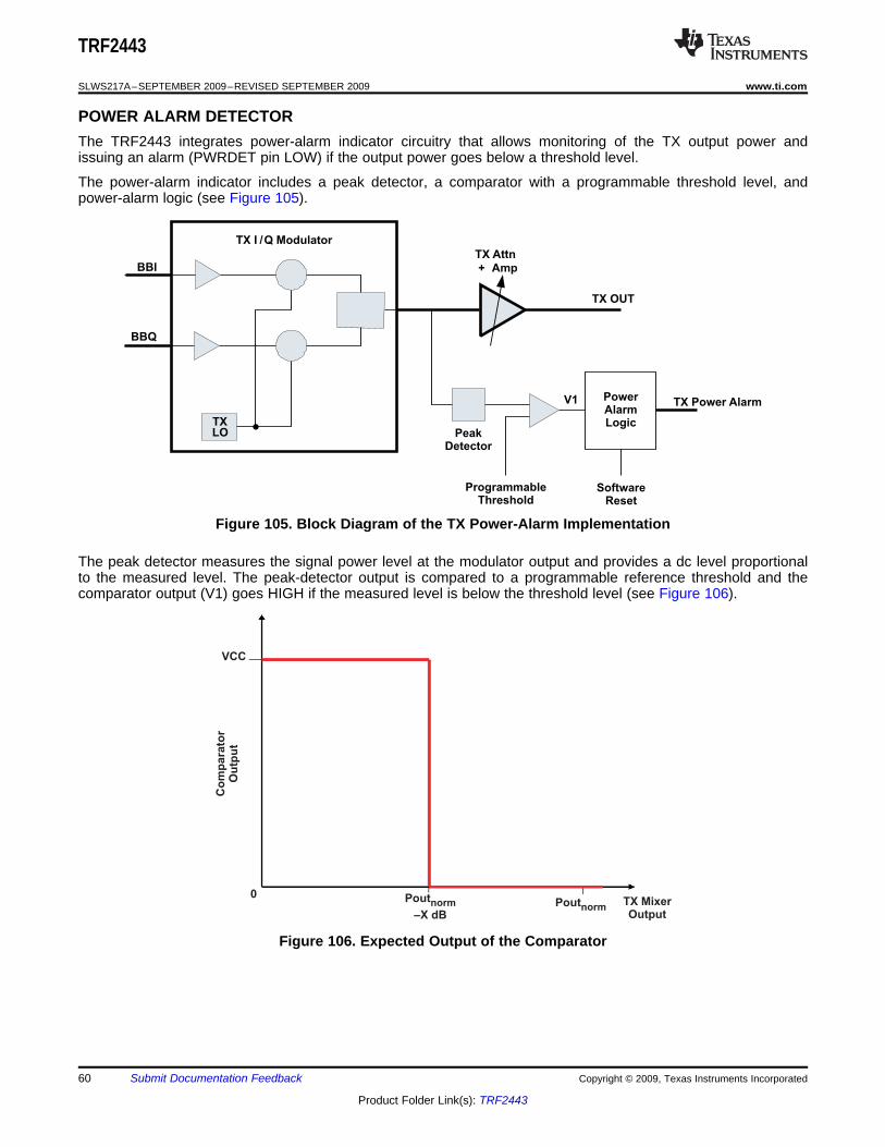
POWER ALARM DETECTOR
TXLO
TX I /Q Modulator
BBI
BBQ
TX Attn
+ Amp
TX OUT
PeakDetector
ProgrammableThreshold
PowerAlarmLogic
TX Power AlarmV1
SoftwareReset
VCC
Co
mp
ara
tor
Ou
tpu
t
Pout
–X dBnorm Poutnorm
0TX MixerOutput
TRF2443
SLWS217A–SEPTEMBER 2009–REVISED SEPTEMBER 2009 ................................................................................................................................... www.ti.com
The TRF2443 integrates power-alarm indicator circuitry that allows monitoring of the TX output power andissuing an alarm (PWRDET pin LOW) if the output power goes below a threshold level.
The power-alarm indicator includes a peak detector, a comparator with a programmable threshold level, andpower-alarm logic (see Figure 105).
Figure 105. Block Diagram of the TX Power-Alarm Implementation
The peak detector measures the signal power level at the modulator output and provides a dc level proportionalto the measured level. The peak-detector output is compared to a programmable reference threshold and thecomparator output (V1) goes HIGH if the measured level is below the threshold level (see Figure 106).
Figure 106. Expected Output of the Comparator
60 Submit Documentation Feedback Copyright © 2009, Texas Instruments Incorporated
Product Folder Link(s): TRF2443
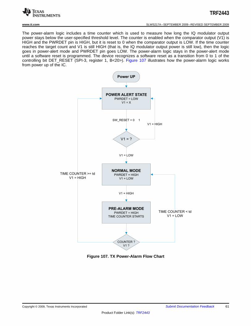
Power UP
POWER ALERT STATE
PWRDET = LOW
V1 = X
V1 = ?
SW_RESET = 0 1
V1 = HIGH
NORMAL MODE
PWRDET = HIGH
V1 = LOW
V1 = LOW
PRE-ALARM MODE
PWRDET = HIGH
TIME COUNTER STARTS
V1 = HIGH
COUNTER ?
V1 ?
TIME COUNTER >= td
V1 = HIGH
TIME COUNTER < td
V1 = LOW
TRF2443
www.ti.com ................................................................................................................................... SLWS217A–SEPTEMBER 2009–REVISED SEPTEMBER 2009
The power-alarm logic includes a time counter which is used to measure how long the IQ modulator outputpower stays below the user-specified threshold level. The counter is enabled when the comparator output (V1) isHIGH and the PWRDET pin is HIGH, but it is reset to 0 when the comparator output is LOW. If the time counterreaches the target count and V1 is still HIGH (that is, the IQ modulator output power is still low), then the logicgoes in power-alert mode and PWRDET pin goes LOW. The power-alarm logic stays in the power-alert modeuntil a software reset is programmed. The device recognizes a software reset as a transition from 0 to 1 of thecontrolling bit DET_RESET (SPI-3, register 1, B<20>). Figure 107 illustrates how the power-alarm logic worksfrom power up of the IC.
Figure 107. TX Power-Alarm Flow Chart
Copyright © 2009, Texas Instruments Incorporated Submit Documentation Feedback 61
Product Folder Link(s): TRF2443
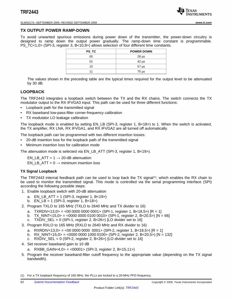
TX OUTPUT POWER RAMP-DOWN
LOOPBACK
TX Signal Loopback
TRF2443
SLWS217A–SEPTEMBER 2009–REVISED SEPTEMBER 2009 ................................................................................................................................... www.ti.com
To avoid unwanted spurious emissions during power down of the transmitter, the power-down circuitry isdesigned to ramp down the output power gradually. The ramp-down time constant is programmable.PS_TC<1,0> (SPI-3, register 3, B<10,9>) allows selection of four different time constants.
PS_TC POWER DOWN00 28 µs01 42 µs10 57 µs11 75 µs
The values shown in the preceding table are the typical times required for the output level to be attenuatedby 30 dB.
The TRF2443 integrates a loopback switch between the TX and the RX chains. The switch connects the TXmodulator output to the RX IFVGA3 input. This path can be used for three different functions:• Loopback path for the transmitted signal• RX baseband low-pass-filter corner-frequency calibration• TX modulator LO leakage calibration
The loopback mode is enabled by setting EN_LB (SPI-3, register 1, B<18>) to 1. When the switch is activated,the TX amplifier, RX LNA, RX IFVGA1, and RX IFVGA2 are all turned off automatically.
The loopback path can be programmed with two different insertion losses:• 20-dB insertion loss for the loopback path of the transmitted signal• Minimum insertion loss for calibration mode
The attenuation mode is selected via EN_LB_ATT (SPI-3, register 1, B<19>).
EN_LB_ATT = 1 → 20-dB attenuationEN_LB_ATT = 0 → minimum insertion loss
The TRF2443 internal feedback path can be used to loop back the TX signal (1), which enables the RX chain tobe used to monitor the transmitted signal. This mode is controlled via the serial programming interface (SPI)according the following possible steps:1. Enable loopback switch with 20-dB attenuation
a. EN_LB_ATT = 1 (SPI-3, register 1, B<19>)b. EN_LB = 1 (SPI-3, register 1, B<18>)
2. Program TXLO to 165 MHz (TXLO to 2640 MHz and TX divider to 16)a. TXRDIV<13,0> = <00 0000 0000 0001> (SPI-1, register 1, B<18,5>) [R = 1]b. TX_NINT<15,0> = <0000 0000 0100 0010> (SPI-1, register 2, B<20,5>) [N = 66]c. TXDIV_SEL = 0 (SPI-1, register 2, B<26>) [LO divider set to 16]
3. Program RXLO to 165 MHz (RXLO to 2640 MHz and RX divider to 16)a. RXRDIV<13,0> = <00 0000 0000 0001> (SPI-2, register 1, B<18,5>) [R = 1]b. RX_NINT<15,0> = <0000 0000 1000 0100> (SPI-2, register 2, B<20,5>) [N = 132]c. RXDIV_SEL = 0 (SPI-2, register 2, B<26>) [LO divider set to 16]
4. Set receiver baseband gain to 10 dBa. RXBB_GAIN<4,0> = <00001> (SPI-3, register 2, B<15,11>)
5. Program the receiver baseband-filter cutoff frequency to the appropriate value (depending on the TX signalbandwidth).
(1) For a TX loopback frequency of 165 MHz, the PLLs are locked to a 20-MHz PFD frequency.
62 Submit Documentation Feedback Copyright © 2009, Texas Instruments Incorporated
Product Folder Link(s): TRF2443

Baseband-Filter Cutoff-Frequency Calibration
LPF BW Adj (dec)
0
2
4
6
8
10
12
14
16
0 10 20 30 40 50 60 70 80 90 100 110 120
RX
BB
Filt
er B
W
G070
RXBB I
RXBB Q
LPF BW Adj (dec)
0.0
0.1
0.2
0.3
0.4
0.5
0.6
0.7
0 10 20 30 40 50 60 70 80 90 100 110 120
RX
BB
Filt
er 1
/BW
G071
RXBB I
RXBB Q
TRF2443
www.ti.com ................................................................................................................................... SLWS217A–SEPTEMBER 2009–REVISED SEPTEMBER 2009
The TRF2443 internal feedback path can be used to set up an automatic calibration of the RX baseband-filtercutoff frequency. The procedure to calibrate the corner frequency to 3 MHz is described as follows.1. Enable loopback switch with minimum insertion loss.
a. EN_LB_ATT = 0 (SPI-3, register 1, B<19>)b. EN_LB = 1 (SPI-3, register 1, B<18>)
2. Program RXLO to 165 MHz (RXLO to 2640 MHz and RX divider to 16).a. RXRDIV<13,0> = <00 0000 0000 0001> (SPI-2, register 1, B<18,5>) [R = 1]b. RX_NINT<15,0> = <0000 0000 1000 0100> (SPI-2, register 2, B<20,5>) [N = 132]c. RXDIV_SEL = 0 (SPI-2, register 2, B<26>) [LO divider set to 16]
3. Set TXVCO divider to 16.a. TXDIV_SEL = 0 (SPI-1, register 2, B<26>) [LO divider set to 16]
4. Set the TXPLL PFD frequency to 4 MHz (R divider = 5).a. TXRDIV<13,0> = <00 0000 0000 0101> (SPI-1, register 1, B<18,5>) [R = 5]
5. Apply a dc offset at the TRF2443 TX baseband inputs (to increase the TXLO leakage at the modulatoroutput).
6. Set the RX baseband amplifier gain to 22 dB.a. RXBB_GAIN<4,0> = <01101> (SPI-3, register 2, B<15,11>)
7. Set the RX baseband cutoff-frequency bit controls RXBB_FREQ<6,0> = 011 1000 (typical value for fC = 3MHz)
8. Program the TXLO frequency to 166 MHz (TXVCO = 2656 MHz).a. TX_NINT<15,0> = <0000 0001 0100 1100> (SPI-1, register 2, B<20,5>) [N = 332]
9. Measure the RX baseband output-power level (at I or Q output): Pout1.10. Program the TXLO frequency to 168 MHz (TXVCO = 2688 MHz).
a. TX_NINT<15,0> = <0000 0001 0101 0000> (SPI-1, register 2, B<20,5>) [N = 336]11. Measure the RX baseband output power level (Pout2) and calculate attenuation: Att = Pout1 – Pout2.12. If Att < 3 dB, then increase RXBB_FREQ and go back to 11); else if Att > 3 dB, then reduce RXBB_FREQ
and go back to 11). This is repeated until two sequential iterations result in the calculated attenuation beingabove and below 3 dB. When this is observed, save the RXBB_FREQ value which results in an attenuationvalue closer to 3 dB.
The TRF2443 baseband low-pass filter cutoff frequency can be programmed to any of 128 cutoff frequencies.The cutoff frequency control consists of 7 bits, RXBB_FREQ<6,0>, which are located in SPI-3, register 2,B<22,16>. RXBB_FREQ<6,0> = <111 1111> corresponds to the minimum corner frequency. Figure 108 showsthe 3-dB bandwidth of the filter versus all possible SPI codes for a typical unit. Figure 109 shows the inverse ofthe 3-dB bandwidth versus all possible SPI codes for a typical unit.
Figure 108. BW vs SPI Code (RXBB_FREQ<6,0> Figure 109. 1/BW vs SPI Code (RXBB_FREQ<6,0>
Copyright © 2009, Texas Instruments Incorporated Submit Documentation Feedback 63
Product Folder Link(s): TRF2443
TX LO Leakage Calibration
RX IMAGE REJECTION
2
2
A 2Acos 1Rejection(dB) = 10log
A 2Acos 1
é ù- +ê ú
+ +ê úë û
f
f
DC-OFFSET CALIBRATION
TRF2443
SLWS217A–SEPTEMBER 2009–REVISED SEPTEMBER 2009 ................................................................................................................................... www.ti.com
Because the corner frequency is dependent on the on-chip capacitance, it is possible to observe variations fromunit to unit in the SPI code that yields a fixed corner frequency. Variations in capacitance from unit to unit resultin a unique 1/BW curve for each unit. If the same DUT is to be used at multiple corner frequencies, the usershould calibrate the DUT as described above to determine, at a minimum, 2 points on the 1/BW curve. Fromthese calibrated points, any other corner frequency can be extrapolated using linear regression.
The TRF2443 internal feedback path can be used to set up an automatic calibration of the TX LO leakageaccording the following potential procedure:1. Enable loopback switch with minimum insertion loss.
a. EN_LB_ATT = 0 (SPI-3, register 1, B<19>)b. EN_LB = 1 (SPI-3, register 1, B<18>)
2. Set RXLO = 330 MHz (RXVCO to 2640 MHz and RX divider to 8)a. RXRDIV<13,0> = <00 0000 0000 0001> (SPI-2, register 1, B<18,5>) [R = 1]b. RX_NINT<15,0> = <0000 0000 1000 0100> (SPI-2, register 2, B<20,5>) [N = 132]c. RXDIV_SEL = 1 (SPI-2, register 2, B<26>) [LO divider set to 8]
3. Set RX baseband in filter bypass mode and gain = 22 dBa. RXBB_GAIN<4,0> = <01101> (SPI-3, register 2, B<15,11>) [gain = 22 dB]b. RXBB_FLT_BYP = 1 (SPI-3, register 2, B<23>) [bypass filter]
4. Program TX LO in normal mode (TXLO = 340 MHz).a. TXRDIV<13,0> = <00 0000 0000 0001> (SPI-1, register 1, B<18,5>) [R = 1]b. TX_NINT<15,0> = <0000 0000 0100 0100> (SPI-1, register 2, B<20,5>) [N = 68]c. TXDIV_SEL = 1 (SPI-1, register 2, B<26>) [LO divider set to 8]
5. Measure power level at RXBB output at 10 MHz = P1.6. Change TX input dc offset until minimum P1 is achieved.
The TRF2443 TX baseband inputs can be ac- or dc-coupled to the external digital-to-analog converter (DAC). Incase of direct coupling, the DAC must provide the appropriate dc offset of step 6 to null the LO leakage. If anac-coupled approach is selected, then the internal bias must be enabled by setting EN_TXCM = 1 (SPI-3,register 3, B<31>). In this case, the integrated dc DAC controls the baseband dc offset. The internal DAC isprogrammed via the SPI. TXBBI<5,0> (SPI-3, register 3, B<30,25>) and TXBBQ<5,0> (SPI-3, register 3,B<24,19>) control the internal DAC settings.
TXBBI<5,0> = TXBBQ<5,0> = <10 0000> corresponds to midrange, that is, no offset applied.
The TRF2443 has been designed to provide optimal image rejection. Using symmetry in the design of the I andQ paths of the receiver ensures that mismatch between the I and Q paths is minimized. Image rejection is afunction of the amplitude (A) mismatch and the phase error (Φ) from 90 degrees of the I and Q RX basebandsignals. Image rejection is calculated in the following manner:
The TRF2443 provides an automatic calibration procedure for adjusting the dc offset in the receiver and XPICbaseband I/Q paths. The internal calibration requires a clock in order to function. This clock is derived internallyfrom the reference clock with a frequency divider, whose divider ratio is programmable. DCOFF_CLK<2,0>(SPI-3, register 5, B<16,14>) and XDCOFF_CLK<2,0> (SPI-3, register 5, B<29,27>) set the division ratio for thedc-offset correction-loop clock for the receiver and XPIC chains, respectively.
The output full-scale range of the internal dc-offset-correction DAC is programmable using bitsDCOFF_BIAS<1,0> (SPI-3, register 5, B<13,12>) for the receiver chain and XPICDCOFF_BIAS<1,0> (SPI-3,register 5, B<26,25>) for the XPIC chain. The range is shown in Table 11.
64 Submit Documentation Feedback Copyright © 2009, Texas Instruments Incorporated
Product Folder Link(s): TRF2443
TEMPERATURE SENSOR
TRF2443
www.ti.com ................................................................................................................................... SLWS217A–SEPTEMBER 2009–REVISED SEPTEMBER 2009
Table 11. DC Offset Correction DAC Programmable RangeDCOFF_BIAS _B1 DCOFF_BIAS _B0 FULL SCALE
XPICDCOFF_BIAS _B1 XPICDCOFF_BIAS _B00 0 10 mV0 1 20 mV1 0 30 mV1 1 40 mV
The I- and Q-channel output maximum dc-offset correction range can be calculated by multiplying the values inTable 11 by the baseband PGA gain. The LSB of the digital correction is dependent on the programmedmaximum correction range. The dc offset correction DAC output is affected by a change in the PGA gain, but ifthe initial calibration yields optimum results, then the adjustment of the PGA gain during normal operation doesnot significantly impair the dc offset balance.
The dc offset correction DACs are programmed from the internal registers when the RXBB_CALSELECT bit(SPI-3, register 7, B<21>) is set to 1 (default value at power on). At start-up, the internal registers are loaded athalf-scale, corresponding to a decimal value of 128. The autocalibration for the receiver chain is initiated bysetting the EN_BB_AUTOCAL bit (SPI-3, register 5, B<5>) to 1. When the calibration is over, this bit isautomatically reset to 0. Similarly for the XPIC, by programming EN_XPIC_AUTOCAL (SPI-3, register 5, B<18>)to 1, the baseband dc-offset calibration starts. During calibration, the RX local oscillator must be on. At eachclock cycle during an autocalibration sequence, the internal circuitry senses the output dc offset and calculatesthe new dc current for the DAC. After the 13th clock cycle, the calibration is complete and the EN_BB_AUTOCAL(or EN_XPIC_AUTOCAL) bit is reset to 0. The dc-offset DAC state is stored in the internal registers andmaintained as long as the power supply is kept on or until a new calibration is started.
The required clock speed for the optimum calibration is determined by the internal detector behavior (integrationbandwidth, gain, sensitivity). The speed of the clock can be slowed down by selecting a clock divider ratioDCOFF_CLK<2,0> (SPI-3, register 5, B<16,14>) and/or XDCOFF_CLK<2.0> (SPI-3, register 5, B<29,27>). Thedetector has more averaging time the slower the clock; hence, it can be desirable to slow down the clock speedfor a given condition to achieve optimum results.
The internal registers controlling the internal dc current DAC for the receiver chain are accessible through theSPI (SPI-3, register 7, B<20,5>), providing a user-programmable method for implementing the dc-offsetcalibration. To employ this option, the RXBB_CALSELECT (SPI-3, register 7, B<21>) bit must be set to 0. Duringthis calibration, an external instrument monitors the output dc offset between the I/Q differential outputs andprograms the internal registers RXBBI_DCOFF<7,0> (SPI-3, register 7, B<12,5) and RXBBQ_DCOFF<7,0>,(SPI-3, register 7, B<20,13) to cancel the dc offset.
The TRF2443 integrates a temperature sensor that can be used to monitor the die junction temperature. Toenable it, PWD_TEMPSENS (SPI-3, register 4, B<22>) must be set to 0. The temperature sensor generates a dcvoltage proportional to the measured temperature. This voltage is output at the TEMPOUT pin (pin 37). Theoutput voltage goes typically from 500 mV at –40°C to 970 mV at 150°C.
The temperature sensor output can also be read through the SPI. An internal ADC converts the analoginformation to digital bits. The internal data-converter is enabled by setting PWD_TEMPADC (SPI-3, register 4,B<21>) to 0. The conversion starts when ADC_START (SPI-3, register 4, B<5>) is set to 1. The internal ADCuses a clock (ADC clock) generated from the external reference clock with a divide-by-16 frequency divider. Atthe end of conversion, ADC_START is reset to 0 and the 8-bit word ADC output is transferred into SPI-3, register0, B<29,22>, where it can be read through the readback mode (See the READBACK MODE section). When thedata conversion from analog to digital is complete, the CONVDONE bit (SPI-3, register 0, B<5>) is set to 1. If theADC input signal is outside its input voltage range, the OUTRANGE bit (SPI-3, register 0, B<6>) is 1. The ADCinput voltage range is 1 V, from 0.125 V to 1.125 V.
Copyright © 2009, Texas Instruments Incorporated Submit Documentation Feedback 65
Product Folder Link(s): TRF2443
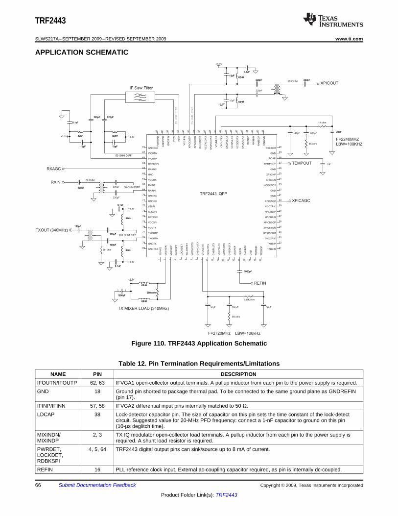
APPLICATION SCHEMATIC
+3.3V
+3.3V +3.3V
+3.3V
+3.3V
+3.3V
+3.3V
RXAGC
XPICAGC
RXIN
TXOUT (340MHz)
REFIN
TEMPOUT
XPICOUT
50 OHM DIFF
50 OHM DIFF
50 OHM DIFF
50 OHM
200 OHM DIFF
50 OHM
75 OHM DIFF
F=2240MHZLBW=100KHZ
F=2720MHz LBW=100kHz
TX MIXER LOAD (340MHz)
50 ohm 39nH39nH
0.1uF0.1uF
220pF
82nH82nH
680pF
220pF220pF
82nH82nH
68nH68nH
220pF
0.1uF0.1uF
47pF
1nF
82nH82nH
15pF15pF
15pF15pF
220pF220pF
68nH68nH
100pF100pF
15pF15pF
220pF220pF
590 ohm590 ohm
15pF
1000pF1000pF
12
56pF
220pF220pF
56pF
100pF100pF
5K ohm
39nH39nH
1.25K ohm
560pF
0.1uF0.1uF
220pF220pF
TRF2443 QFP
IFOUTN62
IFOUTP63
RDBKSPI64
RXAGC65
GND66
RXINP68
RXINN69
GNDRX70
GNDRX71
CLKSPI73
DATASPI74
VCCSPI75
VCCTX76
TXOUTP77
TXOUTN78
GNDTX79
TX
PW
D1
MIX
IND
N2
MIX
IND
P3
PW
RD
ET
4
LO
CK
DE
T5
TX
LO
TE
ST
6
VC
CV
CO
TX
7
VT
UN
ET
X9
CP
OU
TT
X1
0
VC
CP
LLT
X1
2
VC
CD
IGT
X1
3
VC
CR
EF
15
RE
FIN
16
GN
DR
EF
17
TX
BB
QN
19
TX
BB
QP
20
TXBBIN21
TXBBIP22
GNDXPIC23
XPICBBCM24
XPICBBQN25
XPICBBQP26
XPICBBIN27
XPICBBIP28
VCCXPIC29
XPICAGC30
VCCXPIC233
XPICINN34
XPICINP35
TEMPOUT37
LDCAP 38
RXBBCM40
RX
BB
QN
41
RX
BB
QP
42
RX
BB
IN4
3
RX
BB
IP4
4
VC
CD
IGR
X4
6
XP
ICO
UT
P5
5
VC
CIF
I N5
6
IFIN
P5
7
IFIN
N5
8
VC
CP
LL
RX
47
CP
OU
TR
X4
9
VT
UN
ER
X5
0
VC
CV
CO
RX
52
RX
LO
TE
ST
53
XP
ICO
UT
N5
4
GN
DIF
IN2
60
GND32
GNDRX361
VCCRX67
LESPI72
GND31
GNDTX280
GN
DV
CO
TX
8
GN
DP
LLT
X11
GND36
GND39
GN
DIF
IN5
9
GN
DV
CO
RX
51
GN
DP
LL
RX
48
GN
DD
IGR
X4
5
GN
DD
IGT
X1
4
GN
D1
8
PW
RP
AD
81
1000pF1000pF
1K ohm
0.1uF0.1uF
22pF22pF
82nH82nH
220pF
100pF100pF
4K ohm
IF Saw Filter
TRF2443
SLWS217A–SEPTEMBER 2009–REVISED SEPTEMBER 2009 ................................................................................................................................... www.ti.com
Figure 110. TRF2443 Application Schematic
Table 12. Pin Termination Requirements/LimitationsNAME PIN DESCRIPTION
IFOUTN/IFOUTP 62, 63 IFVGA1 open-collector output terminals. A pullup inductor from each pin to the power supply is required.GND 18 Ground pin shorted to package thermal pad. To be connected to the same ground plane as GNDREFIN
(pin 17).IFINP/IFINN 57, 58 IFVGA2 differential input pins internally matched to 50 Ω.LDCAP 38 Lock-detector capacitor pin. The size of capacitor on this pin sets the time constant of the lock-detect
circuit. Suggested value for 20-MHz PFD frequency: connect a 1-nF capacitor to ground on this pin(10-µs deglitch time).
MIXINDN/ 2, 3 TX IQ modulator open-collector load terminals. A pullup inductor from each pin to the power supply isMIXINDP required. A shunt load resistor is required.PWRDET, 4, 5, 64 TRF2443 digital output pins can sink/source up to 8 mA of current.LOCKDET,RDBKSPIREFIN 16 PLL reference clock input. External ac-coupling capacitor required, as pin is internally dc-coupled.
66 Submit Documentation Feedback Copyright © 2009, Texas Instruments Incorporated
Product Folder Link(s): TRF2443

TRF2443
www.ti.com ................................................................................................................................... SLWS217A–SEPTEMBER 2009–REVISED SEPTEMBER 2009
Table 12. Pin Termination Requirements/Limitations (continued)NAME PIN DESCRIPTION
RXAGC 65 Receiver-chain VGA gain-control dc-voltage input. Equivalent input impedance: 100 kΩ in series with 4pF.
RXINP/ RXINN 68, 69 RX input differential terminals. Input impedance is 50 Ω differential. A 1:1 balun is required to drive itsingle-ended.
RXLOTEST 53 RX VCO output pin: test output to check internal RX local oscillator. If it is not used, the pin can begrounded.
TEMPOUT 37 Temperature-sensor output. If temperature sensor is not used (disabled), this pin should be terminatedwith a 100-kΩ resistor to ground. If it used, the TEMPOUT buffer can drive impedances of R > 10 kΩ andC < 100 pF.
TXLOTEST 6 TX VCO output pin: test output to check internal TX local oscillator. If it is not used, the pin can begrounded.
TXBBIP/ TXBBIN 22, 21 TX baseband I-channel differential inputs. If EN_TXCM (SPI-3, register 3, B<31>) = 0, external ACcoupling caps and 100-Ω differential resistor is required.
TXBBQP/ 20, 19 TX baseband Q-channel differential inputs. If EN_TXCM (SPI-3, register 3, B<31>) = 0, external ACTXBBQN coupling caps and 100-Ω differential resistor is required.TXOUTP/ 77, 78 TX amplifier open-collector output terminals. A pullup inductor from each pin to power supply is required.TXOUTN Output impedance is set typically to 200 Ω differential. A 4:1 impedance-ratio balun is needed to
transform to 50 Ω single-ended.TXPWD 1 TX power down; digital inputVCCRX 67 RX-chain power supply. The decoupling capacitor on this power supply should be connected to the same
ground plane to which the GNDRX pins, 70 and 71, are connected.XPICAGC 30 XPIC chain VGA gain-control dc-voltage input. Equivalent input impedance: 100 kΩ in series with 4 pF.XPICOUTN/ 54, 55 XPIC output-amplifier open-collector output terminals. Output impedance is set typically to 75 ΩXPICOUTP differential with an internal resistor so that no external load is required. A pullup inductor from each pin to
the power supply is required. A 1:1 impedance ratio balun is needed to transform to 75 Ω single-ended.
Copyright © 2009, Texas Instruments Incorporated Submit Documentation Feedback 67
Product Folder Link(s): TRF2443
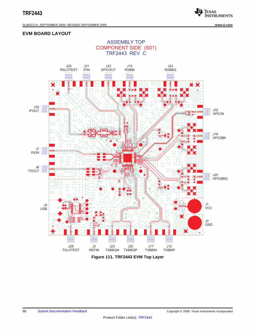
EVM BOARD LAYOUT
J16XPICBBI
J25XPICBBQ
J1VCC
J2GND
J32XPICIN
J7RXIN
J6TXOUT
J5USB
J28TXLOTEST
J3REFIN
J23TXBBQN
J20TXBBQP
J17TXBBIN
J12TXBBIP
J29RXLOTEST
J31IFIN
J33XPICOUT
J15RXBBI
J24RXBBQ
J30IFOUT
ASSEMBLY TOP
TRF2443 REV CCOMPONENT SIDE (S01)
TRF2443
SLWS217A–SEPTEMBER 2009–REVISED SEPTEMBER 2009 ................................................................................................................................... www.ti.com
Figure 111. TRF2443 EVM Top Layer
68 Submit Documentation Feedback Copyright © 2009, Texas Instruments Incorporated
Product Folder Link(s): TRF2443

PACKAGING INFORMATION
Orderable Device Status (1) PackageType
PackageDrawing
Pins PackageQty
Eco Plan (2) Lead/Ball Finish MSL Peak Temp (3)
TRF2443IPFP ACTIVE HTQFP PFP 80 96 Green (RoHS &no Sb/Br)
CU NIPDAU Level-3-260C-168 HR
TRF2443IPFPR ACTIVE HTQFP PFP 80 1000 Green (RoHS &no Sb/Br)
CU NIPDAU Level-3-260C-168 HR
(1) The marketing status values are defined as follows:ACTIVE: Product device recommended for new designs.LIFEBUY: TI has announced that the device will be discontinued, and a lifetime-buy period is in effect.NRND: Not recommended for new designs. Device is in production to support existing customers, but TI does not recommend using this part ina new design.PREVIEW: Device has been announced but is not in production. Samples may or may not be available.OBSOLETE: TI has discontinued the production of the device.
(2) Eco Plan - The planned eco-friendly classification: Pb-Free (RoHS), Pb-Free (RoHS Exempt), or Green (RoHS & no Sb/Br) - please checkhttp://www.ti.com/productcontent for the latest availability information and additional product content details.TBD: The Pb-Free/Green conversion plan has not been defined.Pb-Free (RoHS): TI's terms "Lead-Free" or "Pb-Free" mean semiconductor products that are compatible with the current RoHS requirementsfor all 6 substances, including the requirement that lead not exceed 0.1% by weight in homogeneous materials. Where designed to be solderedat high temperatures, TI Pb-Free products are suitable for use in specified lead-free processes.Pb-Free (RoHS Exempt): This component has a RoHS exemption for either 1) lead-based flip-chip solder bumps used between the die andpackage, or 2) lead-based die adhesive used between the die and leadframe. The component is otherwise considered Pb-Free (RoHScompatible) as defined above.Green (RoHS & no Sb/Br): TI defines "Green" to mean Pb-Free (RoHS compatible), and free of Bromine (Br) and Antimony (Sb) based flameretardants (Br or Sb do not exceed 0.1% by weight in homogeneous material)
(3) MSL, Peak Temp. -- The Moisture Sensitivity Level rating according to the JEDEC industry standard classifications, and peak soldertemperature.
Important Information and Disclaimer:The information provided on this page represents TI's knowledge and belief as of the date that it isprovided. TI bases its knowledge and belief on information provided by third parties, and makes no representation or warranty as to theaccuracy of such information. Efforts are underway to better integrate information from third parties. TI has taken and continues to takereasonable steps to provide representative and accurate information but may not have conducted destructive testing or chemical analysis onincoming materials and chemicals. TI and TI suppliers consider certain information to be proprietary, and thus CAS numbers and other limitedinformation may not be available for release.
In no event shall TI's liability arising out of such information exceed the total purchase price of the TI part(s) at issue in this document sold by TIto Customer on an annual basis.
PACKAGE OPTION ADDENDUM
www.ti.com 23-Sep-2009
Addendum-Page 1
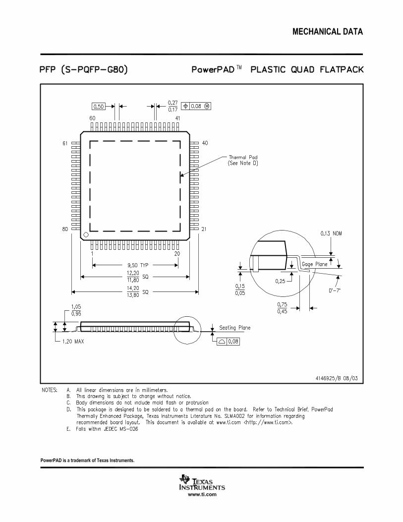

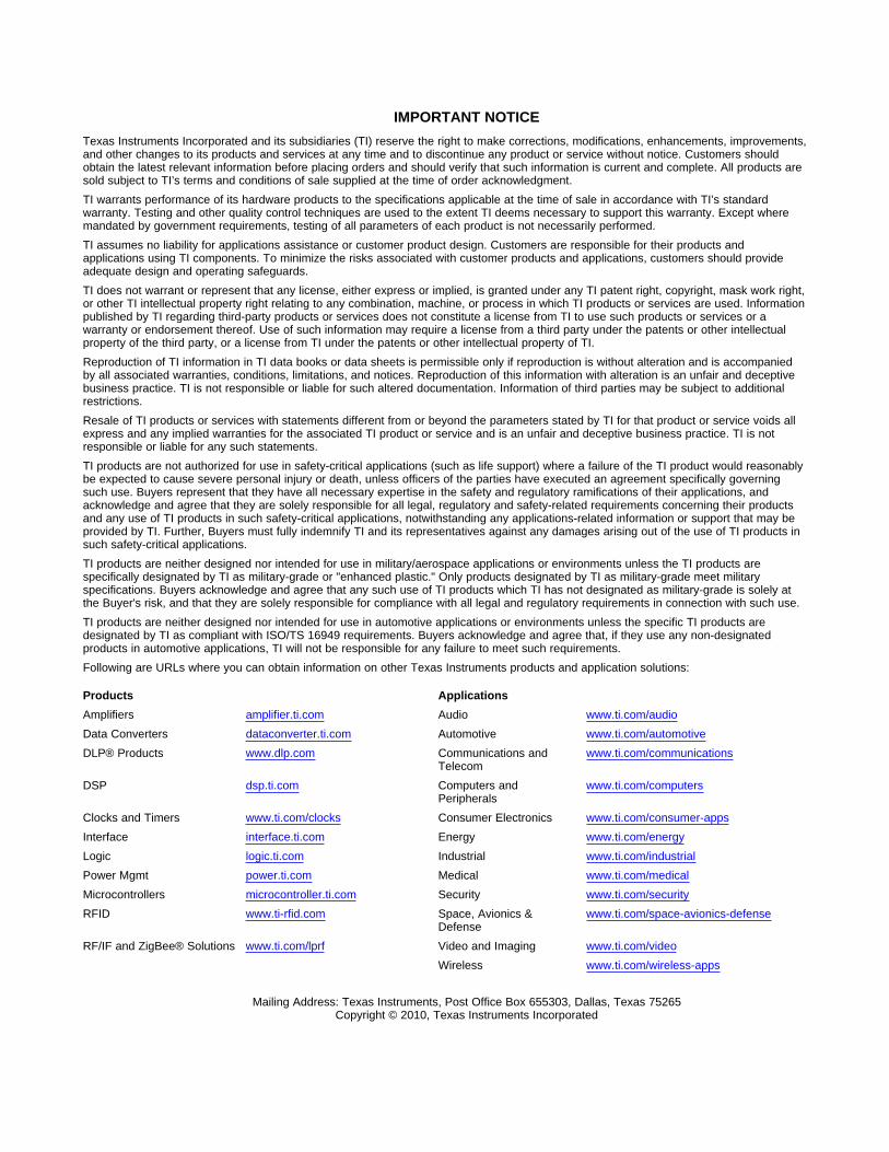
IMPORTANT NOTICE
Texas Instruments Incorporated and its subsidiaries (TI) reserve the right to make corrections, modifications, enhancements, improvements,and other changes to its products and services at any time and to discontinue any product or service without notice. Customers shouldobtain the latest relevant information before placing orders and should verify that such information is current and complete. All products aresold subject to TI’s terms and conditions of sale supplied at the time of order acknowledgment.
TI warrants performance of its hardware products to the specifications applicable at the time of sale in accordance with TI’s standardwarranty. Testing and other quality control techniques are used to the extent TI deems necessary to support this warranty. Except wheremandated by government requirements, testing of all parameters of each product is not necessarily performed.
TI assumes no liability for applications assistance or customer product design. Customers are responsible for their products andapplications using TI components. To minimize the risks associated with customer products and applications, customers should provideadequate design and operating safeguards.
TI does not warrant or represent that any license, either express or implied, is granted under any TI patent right, copyright, mask work right,or other TI intellectual property right relating to any combination, machine, or process in which TI products or services are used. Informationpublished by TI regarding third-party products or services does not constitute a license from TI to use such products or services or awarranty or endorsement thereof. Use of such information may require a license from a third party under the patents or other intellectualproperty of the third party, or a license from TI under the patents or other intellectual property of TI.
Reproduction of TI information in TI data books or data sheets is permissible only if reproduction is without alteration and is accompaniedby all associated warranties, conditions, limitations, and notices. Reproduction of this information with alteration is an unfair and deceptivebusiness practice. TI is not responsible or liable for such altered documentation. Information of third parties may be subject to additionalrestrictions.
Resale of TI products or services with statements different from or beyond the parameters stated by TI for that product or service voids allexpress and any implied warranties for the associated TI product or service and is an unfair and deceptive business practice. TI is notresponsible or liable for any such statements.
TI products are not authorized for use in safety-critical applications (such as life support) where a failure of the TI product would reasonablybe expected to cause severe personal injury or death, unless officers of the parties have executed an agreement specifically governingsuch use. Buyers represent that they have all necessary expertise in the safety and regulatory ramifications of their applications, andacknowledge and agree that they are solely responsible for all legal, regulatory and safety-related requirements concerning their productsand any use of TI products in such safety-critical applications, notwithstanding any applications-related information or support that may beprovided by TI. Further, Buyers must fully indemnify TI and its representatives against any damages arising out of the use of TI products insuch safety-critical applications.
TI products are neither designed nor intended for use in military/aerospace applications or environments unless the TI products arespecifically designated by TI as military-grade or "enhanced plastic." Only products designated by TI as military-grade meet militaryspecifications. Buyers acknowledge and agree that any such use of TI products which TI has not designated as military-grade is solely atthe Buyer's risk, and that they are solely responsible for compliance with all legal and regulatory requirements in connection with such use.
TI products are neither designed nor intended for use in automotive applications or environments unless the specific TI products aredesignated by TI as compliant with ISO/TS 16949 requirements. Buyers acknowledge and agree that, if they use any non-designatedproducts in automotive applications, TI will not be responsible for any failure to meet such requirements.
Following are URLs where you can obtain information on other Texas Instruments products and application solutions:
Products Applications
Amplifiers amplifier.ti.com Audio www.ti.com/audio
Data Converters dataconverter.ti.com Automotive www.ti.com/automotive
DLP® Products www.dlp.com Communications and www.ti.com/communicationsTelecom
DSP dsp.ti.com Computers and www.ti.com/computersPeripherals
Clocks and Timers www.ti.com/clocks Consumer Electronics www.ti.com/consumer-apps
Interface interface.ti.com Energy www.ti.com/energy
Logic logic.ti.com Industrial www.ti.com/industrial
Power Mgmt power.ti.com Medical www.ti.com/medical
Microcontrollers microcontroller.ti.com Security www.ti.com/security
RFID www.ti-rfid.com Space, Avionics & www.ti.com/space-avionics-defenseDefense
RF/IF and ZigBee® Solutions www.ti.com/lprf Video and Imaging www.ti.com/video
Wireless www.ti.com/wireless-apps
Mailing Address: Texas Instruments, Post Office Box 655303, Dallas, Texas 75265Copyright © 2010, Texas Instruments Incorporated