inter satellites optical communication systems for defense i · 1 abstract— satellite...
TRANSCRIPT

1
Abstract— Satellite communication systems are increasingly
more used by the society in many applications, and its
development is a high priority for the scientific community. The
need for increasing bandwidth to satisfy the users’ needs, makes
inter-satellites Free Space Optics (FSO) communication
preferred instead of traditional radio frequency links.
The inter-satellites communication links with high bit rates
and low power is a determining factor in the performance of
these systems. As such communications occur over long distances
and high altitude orbits, optical sources with highly collimated
and coherent beams are needed in order to ensure a better link
between the transmitter and the receiver with low emission
power.
This paper involves the development of two experimental
blocks for implementing an inter-satellite optical communication
system using a semiconductor laser type. It aims at the definition
and analysis of the elements of the two circuits, at the transmitter
subsystem and includes the design for the production of printed
circuit boards (PCB). Moreover, experimental tests were
performed to validate the results obtained in the simulations.
Index Terms— Satellites, Optical Communications,
Transmitter Subsystem, Semiconductor Laser.
I. INTRODUCTION
HE demand for diversified services, such as the use of
high speed internet, videoconference and watching
programs or videos directly on the Internet (streaming) has
resulted in a dramatic increase of the bandwidth required, as
the data rate transmission is determined by the available
bandwidth [1], [2].
Satellites have nowadays several applications of great
importance to the society, such as in telecommunications, in
weather forecast and in earth’s surface observation, on GPS
coordinates navigation (Global Positioning System), and even
in space research. On the military scope the mentioned
applications gain a higher importance in recognition and
surveillance as they are used in the theatre of operations (TO).
The information collected in real time may represent and
advantage to the military leadership enabling their decision
making [2].
The wide spectrum of the optical communications (without
regulation so far), unlike the RF communications, represent an
additional advantage due to the possibility of data rate
transmission of the order of dozens of Gbps [1].
A crucial device to establish the communication between
the satellites is the optical source. The semiconductor lasers
are often considered ideal sources of transmission due to their
high efficiency in the conversion of electrical into optical
power, their small size, their easy integration and their low
energy consumption. Their low cost is also a reason to select
them as the optical source to be used [3], [4].
The purpose of this paper is to define a transmitter
subsystem, operating at optical frequencies, that may be
integrated in a satellite intercommunication system, simulate
the transmitter subsystem, and build and test the several
blocks that constitute this subsystem.
II. STATE OF ART OF THE OPTICAL COMMUNICATIONS INTER-
SATELLITES
A. Satellite Systems Evolution
The development of lasers since the 60’s of the XXth
century, triggered the interest of international agencies of this
technology. The European Space Agency (ESA) developed
the first studies for the use of lasers in inter-satellite
communications. In the beginning of 1991 the first
unidirectional inter-satellite communication link was
established through the program SILEX. The connection was
established between the Pastel optical terminals, on board of
the French ground observation satellite SPOT-4 and OPALE,
installed in the European communications satellite ARTEMIS
[5], [6]. The satellites SPOT-4 and ARTEMIS were set in a
low earth orbit (LEO) and in a geostationary orbit,
respectively. The distance between them is approximately
45000 km and while SPOT-4 transmitted images at 50 Mbps
rate to ARTEMIS, this satellite would retransmit them to
Earth almost in real time. To establish this connection a laser
with a power transmission of 60 mW was used, with a
wavelength of 0.8 µm and OOK modulation [4], [7].
In 2008 a successful demonstration of an optical inter-
satellite connection (between satellites TerraSAR-X and
NFIRE) on the low earth orbit was established. The LCTs
enabled the increase of the users’ data traffic compared to the
radiofrequency connections and they are, nowadays, the most
used modules in the industry to establish inter-satellite optical
communications [4], [8].
B. Conditioning factors to the inter-satellites communication
The satellites can be grouped according to their purpose and
orbit type.
Regarding the purpose, there are communication satellites
which are responsible for voice, TV and Internet transmission.
Inter-satellites Optical Communication Systems
for Defense - I
João Miguel Madeira Trindade, Military Academy/IST
T

2
There are also meteorological, scientific, navigation, earth
observation and military satellites. Military satellites are
essential in navigation assistance and in the positioning of
military forces as well as in surveillance and recognition tasks,
minimizing the enemy’s surprise effect [9].
In what concerns the type of orbit, there are three of
satellites according to their distance from the Earth. In Pic. 1
the three types of orbits are presented.
Picture 1 - Three types of orbits
Low Earth Orbit (LEO): which corresponds to a distance
of 180 to 2000 km from the earth’s surface. This type of
satellites is ideal for military observations, for
meteorological data collection and also for
communications. They consume less operation energy
and they have less launching costs.
Medium Earth Orbit (MEO): corresponding to 2000 km
to 25800 km above the earth’s surface. These are
generally navigation (GPS), communication and
scientific satellites. Their coverage area is wider than
LEO’s.
Geostationary Earth Orbit (GEO): they orbit the Earth at
a 35800 km distance and their orbital period is 24 hours
[10], [11]. They cover a wider area, but they are big
devices, expensive and which demand a lot of energy to
be launched into space.
In general, the orbits at a higher altitude are more stable due
to less interference caused by atmospheric density and by
gravitational fluctuations. The gravitational fields of the
celestial bodies (such as the Moon and the Sun), the solar
radiations and the centrifugal force effect generated by the
Earth’s rotation movement can affect the orbital stability of
the satellites [12].
C. Basic Parameters of the inter-satellites communication
systems
The optical communications established between satellites
occur mainly in the exosphere atmospheric layer (above 500
km) and although the temperatures reach as much as 1000 ºC,
there is no danger of overheating for the satellites as the
atmosphere is extremely rarefied causing a very low heat
exchange. This way there is no attenuation caused by the
atmosphere and it is considered that the electromagnetic field
generated by the transmitter propagates almost in vacuum.
In an optical communication system there must be
communication between the transmitter and the receiver. The
power of the optical signal transmitted is affected by many
factors before reaching the receiver. These factors include loss
of connection route in the free space (𝑙𝑠), pointing losses (𝑙𝑝)
and background radiation. The pointing losses are a result of
the difference between the beam direction and the satellite
position. Regarding the losses due to the divergence of the
beam, they can be calculated considering the opening angles
(θT and θR) and the diameter of the antenna (DT and DR) [5],
[13].
The performance of this system can be obtained through the
power flow equation. The power of the signal received (𝑝𝑅)
[W] depends on the power transmitted (𝑝𝑇) [W], on the
transmitting antenna gain (𝑝𝑇), on the receiving antenna gain
(𝑔𝑅), on the route losses in the free space and on the
transmitter (𝑙𝑝𝑡) and the receiver (𝑙𝑝𝑟) pointing losses.
𝑝𝑅 = 𝑝𝑇 . 𝑔𝑇 . 𝑙𝑝𝑡 . 𝑙𝑠 . 𝑔𝑅 . 𝑙𝑝𝑟 (1)
The antenna gain (𝑔) depends on the lens optical efficiency
(𝜂) and the antenna opening diameter (𝐷) [m] as given by:
𝑔 = 𝜂 (𝜋. 𝐷
𝜆)
2
(2)
This way, the transmitting (𝑔𝑇) and receiving (𝑔𝑅) gain is
calculated considering the opening diameter of the
transmitting and receiving antennas, respectively 𝐷𝑇 𝑎𝑛𝑑 𝐷𝑅 .
The opening angles can be calculated through:
𝜃 = 2.24𝜆
𝐷 (3)
where θT and θR are the opening angles of the transmitting and
receiving antenna in radians. The pointing losses are given by:
𝑙𝑝 = 𝑒−𝑔𝜃2 (4)
The route losses in free space (𝑙𝑠) depend on the length of
the link (𝑑) [m] and are given by:
𝑙𝑠 = (𝜆
4𝜋. 𝑑)
2
(5)
In general, considering the analysis of the above
expressions, the advantages of the FSO system are a result of
the basic characteristics of the laser beam. As can be inferred
from (2) and (5), for higher frequencies higher transmitting
and receiving gains are obtained and less free space losses
occur [5], [13].
III. CHARACTERISTICS OF THE TRANSMITTING SUBSYSTEM
A. Blocks description and diagram
The current FSO systems operate typically in wavelengths
in the near infrared spectrum, between 800 and 1600 nm.
There are some special windows of wavelengths of operation,
more specifically 850, 1310 and 1550 nm. The 1310 and 1550

3
windows match the standard transmitting windows of the
optical fiber communication systems, so the majority of the
FSO commercial systems operate in these two windows in
order to use the most common components. The Ultra-Violet
(UV) wavelength was recently considered for the FSO
systems, because apart from being less subject to pointing
errors and to beam interference it has the advantage of being
less sensible to interferences caused by background radiation
[14], [15]. Pic. 2 shows the electromagnetic spectrum where
we can observe the ultraviolet radiation, visible and infrared
areas.
Picture 2 - Electromagnetic Spectrum
The transmitting system is composed by the optical source,
the modulator, the optical amplifier and in the end there is the
optical beam, as we can see in Pic. 3. The channel encoding
can be performed optionally before modulation; this way the
bits generated by the source are first codified and later
modulated. In order to increase the optical intensity of the
laser beam which was formerly modulated, an optical
amplifier can be used. Then, the light beam is transmitted
through an optical antenna.
Picture 3 - Block diagram of the optical transmitter
The optical source used in FSO systems is generally a
semiconductor laser, although some manufacturers use the
high power LED technology with beam collimators for that
purpose. The most used semiconductors laser types are: the FP
(Fabry-Perot), the DFB (Distributed Feedback) and the
VCSEL (Vertical Cavity Surface Emitting Lasers).
B. Historical evolution of the semiconductor lasers
In 1960 Maiman demonstrated the performance of the first
laser using a ruby crystal, operating in the visible. The first
semiconductor laser, an homogeneous structure device, which
used a p-n junction of GaAs, was developed in 1962 by Hall
[4], [16], [17].
A perpendicular p-n junction plan with two polished end
surfaces has turned the semiconductor into a small FP cavity.
However, the fact that the FP lasers need a high threshold
current caused heating problems in the system [18].
In 1969, was found the first solution to operate at room
temperature with hetero structure semiconductor lasers, type
GaAs/AlGaAs, was found.
In 1990, the need to develop laser amplifiers arose, in order
to establish long haul communications using optical fibers.
The need to transmit several signals simultaneously in the
same physical space – Wavelength Division Multiplexing
(WDM) – led to the development of DFB lasers and DBR
(Distributed Bragg Reflector) lasers. This kind of lasers which
transmit in one single mode increased the frequency stability
of these sustems [4], [19].
Nowadays the most common laser type is the
semiconductor, which has wide application. These type of
lasers is usually preferred to other types, due to their great
efficiency of converting electrical power into optical, their
small size, light weight and possibility of being modulated
directly [4], [20].
C. Types of semiconductor lasers
In the telecommunication systems the FP laser and the DFB
laser are the most commonly used light sources. In the systems
in which data transmission is predominant and when costs are
concerned, such as the GbE (Gigabit Ethernet), the FP laser
and the VCSEL are the most used [21]. In the next section a
description of the composition and main characteristics of the
most used types of semiconductor lasers in optical
connections: the FP, the DFB and the VCSEL, is given.
a) Laser FP (Fabry-Perot)
The simplest structure of a semiconductor laser is an FP
laser, as represented in Pic. 4.
Picture 4 - Structure of an FP laser
To help confining the bearers to the active region (GaAs),
the surrounding doped areas p and n, which in this case are
made of AlGaAs, have a major forbidden band. In the edges
two surfaces mirrors are used to control the light output on the
intended edge.
The FP lasers are not composed by frequency selective
elements, which means they are not Multiple-Longitudinal
Mode lasers (MLM). However, by reducing the size of the
cavity it is possible to get a behavior close to a single mode
laser [4], [21].
b) DBF (Distributed Feedback) laser
This laser has an active area similar to that of a FP laser,
with a built-in corrugation area that acts like a reflector.
Instead of concentrating the reflexivity in the edges of the
cavity, its reflection properties are distributed along the active
area, that is, along the length of the cavity, as presented in Pic.
5.
Mirror
4
Picture 5 - Structure of a DFB laser
The reflections required for a laser operation are due to the
grating, which enables only a specific wavelength. Therefore,
the DBF lasers are Single Longitudinal Mode (SLM) lasers.
These devices are coated with antireflective materials on the
front side and with a high reflexivity coating on the rear side,
in order to guarantee that the light comes out only in one
direction.
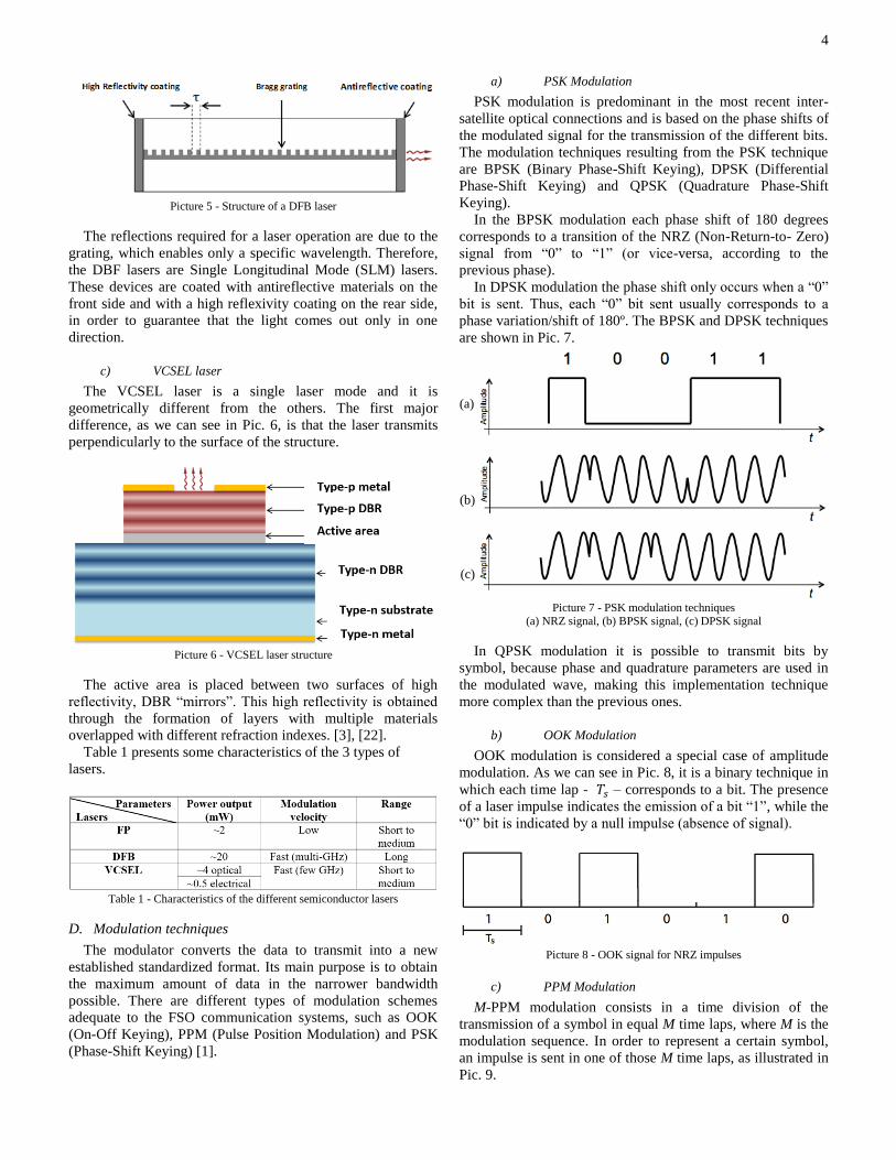
c) VCSEL laser
The VCSEL laser is a single laser mode and it is
geometrically different from the others. The first major
difference, as we can see in Pic. 6, is that the laser transmits
perpendicularly to the surface of the structure.
Picture 6 - VCSEL laser structure
The active area is placed between two surfaces of high
reflectivity, DBR “mirrors”. This high reflectivity is obtained
through the formation of layers with multiple materials
overlapped with different refraction indexes. [3], [22].
Table 1 presents some characteristics of the 3 types of
lasers.
Table 1 - Characteristics of the different semiconductor lasers
D. Modulation techniques
The modulator converts the data to transmit into a new
established standardized format. Its main purpose is to obtain
the maximum amount of data in the narrower bandwidth
possible. There are different types of modulation schemes
adequate to the FSO communication systems, such as OOK
(On-Off Keying), PPM (Pulse Position Modulation) and PSK
(Phase-Shift Keying) [1].
a) PSK Modulation
PSK modulation is predominant in the most recent inter-
satellite optical connections and is based on the phase shifts of
the modulated signal for the transmission of the different bits.
The modulation techniques resulting from the PSK technique
are BPSK (Binary Phase-Shift Keying), DPSK (Differential
Phase-Shift Keying) and QPSK (Quadrature Phase-Shift
Keying).
In the BPSK modulation each phase shift of 180 degrees
corresponds to a transition of the NRZ (Non-Return-to- Zero)
signal from “0” to “1” (or vice-versa, according to the
previous phase).
In DPSK modulation the phase shift only occurs when a “0”
bit is sent. Thus, each “0” bit sent usually corresponds to a
phase variation/shift of 180º. The BPSK and DPSK techniques
are shown in Pic. 7.
Picture 7 - PSK modulation techniques
(a) NRZ signal, (b) BPSK signal, (c) DPSK signal
In QPSK modulation it is possible to transmit bits by
symbol, because phase and quadrature parameters are used in
the modulated wave, making this implementation technique
more complex than the previous ones.
b) OOK Modulation
OOK modulation is considered a special case of amplitude
modulation. As we can see in Pic. 8, it is a binary technique in
which each time lap - 𝑇𝑠 – corresponds to a bit. The presence
of a laser impulse indicates the emission of a bit “1”, while the
“0” bit is indicated by a null impulse (absence of signal).
Picture 8 - OOK signal for NRZ impulses
c) PPM Modulation
M-PPM modulation consists in a time division of the
transmission of a symbol in equal M time laps, where M is the
modulation sequence. In order to represent a certain symbol,
an impulse is sent in one of those M time laps, as illustrated in
Pic. 9.
(a)
(b)
(c)

5
Picture 9 - M-PPM signal
IV. CIRCUITS SIMULATION AND TESTING
Two types of circuits were considered to transmit the
information using the laser source. The first circuit, with
discrete components, was designed to operate below 10 MHz
and the second circuit, composed by integrated components,
was designed to reach frequencies in the GHz band.
A. Circuit with discrete components
The first circuit was divided in three parts; the first part was
composed by a differential pair, the second by two inverter
stages and the third by the laser.
a) Differential Pair
The first part which can be observed in Pic. 10 is a
differential pair composed by two bipolar junction transistors
2n3904 (Q1 and Q2). Their purpose is to work as differential
amplifier, as both transistors are in the operation area of direct
active zone.
Picture 10 - Differential pair with bipolar transistors
In Pic. 11 we can see a simpler version of Pic. 10 to
simplify the DC analysis of the differential pair.
Picture 11 - Differential pair parameters
It is possible to observe all the parameters that constitute the
differential pair in Pic. 11. These parameters are highly
important for the theoretical calculation, enabling the
interpretation of the differential pair operation. Knowing that
the sum of the power failures in a closed circuit is zero,
Kirchhoff Voltage Law (KVL), we can get the following
expressions:
−5 + 𝑅2 𝑖𝐵1 + 𝑉𝐵𝐸1 + 𝑅1 𝑖𝐸 = (6)
−12 + 𝑉𝐶𝐸1 + 𝑅1 𝑖𝐸 = 0 (7)
−12 + 𝑅4 𝑖𝐶2 + 𝑉𝐶𝐸2 + 𝑅1 𝑖𝐸 = 0 (8)
−5 + 𝑅3 𝑖𝐵2 + 𝑉𝐵𝐸2 + 𝑅1 𝑖𝐸 = 0 (9)
The sum of the currents from the TBJ Q1 and TBJ Q2
transmitters equals the current that crosses R1, that is:
𝑖𝐸 = 𝑖𝐸1 + 𝑖𝐸2 (10)
Also knowing that according to the TBJ’s characteristics:
𝑖𝐸𝑥 = 𝑖𝐵𝑥 + 𝑖𝐶𝑥 (11)
𝑖𝐶𝑥 = 𝛽 𝑖𝐵𝑥 (12)
𝑖𝐸𝑥 = (1 + 𝛽)𝑖𝐵𝑥 (13)
Admitting that VBE = 0.7 V and that the current gain figure
is 𝛽 = 200 for both TJBs we get the differential pair
parameters.
In table 2 we can see the theoretical values obtained and the
values simulated in the PSpice program.
6
Parameter Theoretical
value
Simulation value -
PSpice
𝒊𝑩𝟏 = 𝒊𝑩𝟐 13 μA 22.79 μA
𝒊𝑪𝟏 2.601 mA 2.626 mA
𝒊𝑪𝟐 2.601 mA 2.558 mA
𝒊𝑬𝟏 2.614 mA 2.649 mA
𝒊𝑬𝟐 2.614 mA 2.581 mA
𝒊𝑬 5.228 mA 5.229 mA
𝑽𝑩 4.987 V 4.977 V
𝑽𝒐𝒖𝒕 9.867 V 9.900 V
Table 2 - Theoretical and simulated values
The incremental model is valid for small variations of the
input signal and when the differential pair works as a linear
amplifier. While in the differential mode two different
voltages are applied at the base of the transisitors Q1 and Q2,
respectively, 𝑉𝑑
2 and −
𝑉𝑑
2, in the common mode the tensions
applied at the base, 𝑉𝑐 are equal in both transistors.
The expressions of the differential and of the common mode
gain are given, respectively, by:
𝑔𝑑 = 𝑣0
𝑣𝑑
= −1
2𝑔𝑚𝑅4 (14)
𝑔𝑐 = 𝑣0
𝑣𝑐
=𝛽 𝑅4
𝑟𝜋 + 2 (𝛽 + 1)𝑅1 (15)
with R4 = 820 Ω we can obtain a differential mode gain of
𝑔𝑑 = −41 𝑉/𝑉 in linear units and of 𝐺𝑑 = 32.26 𝑑𝐵 in
logarithmic units (in module). In (15) with R1 = 820 Ω we
have a common mode gain of 𝑔𝑐 = 0.5 V/V in linear units and
of 𝐺𝑐 = −6.02 𝑑𝐵 in logarithmic units.
The ratio between the differential mode gain and the
common mode gain is defined as Common Mode Rejection
Ratio (CMRR) and it is given by the expression:
𝐶𝑀𝑅𝑅 = |𝑔𝑑
𝑔𝑐
| (16)
The capacity of the diferential amplifier to reject equal
signals applied to the inputs Vin+ and Vin- (CMMR) amounts
to 38.28 dB.
The TJBs used are npn type and depending on the
polarization condition (direct or inverse) of each junction, they
can operate in four different areas: Cut-off area, Direct or
Inverse Active area and Saturation area. It was found that the
colector, base and transmitter currents are equal and positive
for both transistors; it was admitted that both transmitter base
junctions were conducting and that the voltages at their
terminals were equal to 0,7 V and that the VBC voltages in the
colector base junctions of the two transistors, although of
different value, are both negative. In these conditions the
operation area for both transistors is the direct active area.
To check the circuit’s behavior the PSpice simulator was
used, introducing in the circuit input a rectangular impulse
ranging between 0 V and 5 V for the frequencies of 0.1 MHz
and 10 MHz. In Pic. 12 we can observe the impulse for 10
MHz.
Picture 12 - Input signal Vin, 10 MHz
The signal at the output of the TBJ Q2 (Vout) colector fot
the frequency of 0.1 MHz is represented in Pic. 13.
Picture 13 - Transitional regime of TJB Q2 collector, 0.1 MHz
For this frequency the signal presented in Pic. 14 was
obtained experimentally.
Picture 14 - Tests to the TJB Q2 collector, 0.1 MHz
Comparing the signal obtained in the experimental test with
the PSpice simulation signal, we conclude that there is a slight
decrease of amplitude of 0.4 V. There was also a change of the
duty cycle from 50% to 75 %.
b) Inverter stages
The second part of the electrical circuit is composed by two
inverter stages. Pic. 15 shows the two inverter stages in a
simplified version.
Picture 15 - Inverter stages
The two inverter stages which are part of the circuit have
different roles. In both stages the inverters are connected in
parallel and while the first stage, composed by 3 inverters, has
the purpose of stabilizing the input signal sent from the
9
10
11
12
13
-3,0E-5 -2,0E-5 -1,0E-5 0,0E+0 1,0E-5 2,0E-5 3,0E-5
Volts
Seconds

7
differential pair, the second stage, composed by 15 inverters
has the purpose of supplying more current for the laser.
The signal at the output of the first inverters stage for the
frequency of 0.1 MHz is represented in Pic.16.
Picture 16 - Transitional regime after the 1st inverters stage, 0.1 MHz
Comparing Pic.12 with Pic. 16 the signal inversion is
confirmed, however the main reason for that stage is the
stabilization of the signal. I enable a constant variation
between the same two levels and that it keeps a good
definition in time.
The signal at the output of the second inverters stage for 0.1
MHz frequency is represented in Pic.17.
Picture 17 - Transitional regime after the 2nd inverters stage, 0.1 MHz
As we can in Pic. 17, the transitional regime of this signal is
different, presenting in two time laps two different levels of
voltage. The changing behavior of voltage levels is due to the
voltage limits V1L and V1H, characteristic of the 7404 inverter.
Once the V1L maximum is 0.8 V and the V1H minimum is 2 V,
those axis were drawn in Pic. 18 chart in order to analyse the
observed behavior.
Picture 18 - Characteristics of the 7404 inverter, 0.1 MHz
Apart from V1L and V1H of the inverter 7404 represented in
blue in the picture above, we can also see the impulse in green
before the 2nd stage of inverters and in red after it. Every
green signal below the V1L line is considered a logical value
“0”, above V1H line the logical value considered is “1” and
between those lines there is a non-defined area.
In the experimental test as the inverters used were the
74HCT04 with different voltage levels, no problem occurred
as we can see in Pic. 19.
Picture 19 – Results obtained in the test to the output of the 2nd stage inverters,
0.1 MHz
We can see in the above picture that the signals are similar.
In blue there is the signal introduced through a signal
generator in the experimental circuit and in red the signal at
the output of the second inverters stage. The red signal would
be the signal to be fed to the laser.
B. Circuit with integrated components
Another way of transmitting information using a laser is by
exciting it with integrated circuits of advanced technology,
projected specifically for that purpose. The integrated circuits
MAX3643 and DS1865 are, respectively, a circuit that
controls the laser excitation current and a circuit that checks
the light power transmitted by the laser and adjusts the drive
current in order to keep the light power constant. Pic.20
presents the circuit which enables the information
transmission with those integrated circuits, in this case
projected for high frequencies.
Picture 20 - Circuit for high frequencies
As we can see in Pic. 20 there are several components that
involve the integrated circuit MAX3643. These are the
components (resistors, capacitors and inductors) which
determine the values of currents, voltages and frequencies in
the circuit’s operation.
Resistors R1 and R2 constitute a voltaje divider of the input
signal (Vin) protecting both the integrated circuit and the
laser. The signal transmitted by that voltage splitter is the
input signal in the integrated circuit MAX3643, more
specifically in ports IN+ and BEN+.
While port IN+ is responsible for the acceptance of
information bits, port BEN+ (when active) is responsible for
-4
1
6
-3,0E-5 -2,0E-5 -1,0E-5 0,0E+0 1,0E-5 2,0E-5 3,0E-5
Volts
Seconds

8
the emission of light through the laser. In this case IN+ and
BEN+ ports were connected to the same circuit point, which
means that when the Vin input signal is in low level the laser
is off. When the Vin input is high, the BEN+ input enables the
laser excitation according to the dimensioning performed at
ports MODSET and BCMON, as we can see ahead.
Once the input maximum voltage in the integrated circuit
MAX3643 (in pin IN+) is 0.8 V, from (17) one obtains:
𝑉𝐼𝑁+ =𝑅2
𝑅2 + 𝑅1∙ 𝑉𝑖𝑛 (17)
Fort he input signal Vin the same rectangular impulse was
considered, but for calculation effects only its maximum
value, 5 V was taken into account. Once the relation between
𝑉𝐼𝑁+ and Vin is 0.16, the resistors values were 100 Ω for R2
and 560 Ω for R1.
Taking into account that the laser has a current threshold
value of to varying between 24 mA and 30 mA and an
operating current between 33 mA and 40 mA, the maximum
current at the output of the integrated MAX3643, on pin
IMAX (𝐼𝑀𝐴𝑋) is given by (18).
𝐼𝑀𝐴𝑋 = 𝐼𝐵𝐼𝐴𝑆 + 𝐼𝑀𝑂𝐷 (18)
The current modulation, 𝐼𝑀𝑂𝐷 , and the forward bias current,
𝐼𝐵𝐼𝐴𝑆 , are turned off if their sum exceeds the limit set by the
resistor of the pin IMAX (𝑅𝐼𝑀𝐴𝑋). It was chosen for the
current 𝐼𝐵𝐼𝐴𝑆 the value of 33 mA and to the current 𝐼𝑀𝑂𝐷 the
value of 5 mA. It is now possible to control the maximum
current to the output of the controller by choosing
appropriately the value of 𝑅𝐼𝑀𝐴𝑋 . For a current 𝐼𝑀𝐴𝑋 of 38
mA the use of a resistor in the pin IMAX 15 kΩ, will prevent
the laser from burning.
To be able to control both the chain of modulation 𝐼𝑀𝑂𝐷 as
the forward bias current 𝐼𝐵𝐼𝐴𝑆, two resistors are introduced in
the circuit, respectively 𝑅𝑀𝑂𝐷𝑆𝐸𝑇 and 𝑅𝐵𝐶𝑀𝑂𝑁. The resistor
value of 𝑅𝑀𝑂𝐷𝑆𝐸𝑇 can be obtained, according to the
specifications of the controller MAX3643, through (19).
𝑅𝑀𝑂𝐷𝑆𝐸𝑇 = 1.2 ∙ 𝐺𝑀𝑂𝐷
𝐼𝑀𝑂𝐷
− 𝑅𝑀𝑂𝐷 (19)
where 𝑅𝑀𝑂𝐷 and 𝐺𝑀𝑂𝐷, are typically 50 Ω and 88 mA/mA
and denote respectively, the internal resistor of the pin
MODSET and current gain modulation. The resistor value of
𝑅𝑀𝑂𝐷𝑆𝐸𝑇 should be chosen to produce the maximum current
of modulation to the operating temperature of the laser. For a
chain of modulation 𝐼𝑀𝑂𝐷 of 5 mA, the resistor value
𝑅𝑀𝑂𝐷𝑆𝐸𝑇 is 21.07 kΩ. Thus, it is assumed for the resistor
𝑅𝑀𝑂𝐷𝑆𝐸𝑇 the value of 18 kΩ which corresponds to a chain of
modulation 𝐼𝑀𝑂𝐷 of 5.85 mA.
The resistor 𝑅𝐵𝐶𝑀𝑂𝑁 is obtained from the current gain of
polarization, 𝐺𝐵𝑆𝑀, and imposing that the voltage at the
terminals, 𝑉𝐵𝐶𝑀𝑂𝑁, must be less than 1.4 V. The resistor
𝑅𝐵𝐶𝑀𝑂𝑁 is determined according to the specifications of the
controller MAX3643, through (20).
𝑅𝐵𝐶𝑀𝑂𝑁 = 𝑉𝐵𝐶𝑀𝑂𝑁
𝐼𝐵𝐼𝐴𝑆 ∙ 𝐺𝐵𝑆𝑀
(20)
For a current 𝐼𝐵𝐼𝐴𝑆 of 33 mA, with a gain 𝐺𝐵𝑆𝑀 of 17 mA/A
get a resistor 𝑅𝐵𝐶𝑀𝑂𝑁 of 3.03 kΩ is obtained. Thus, it is for
the resistor 𝑅𝐵𝐶𝑀𝑂𝑁 the value of 3.3 kΩ which will have a
current 𝐼𝐵𝐼𝐴𝑆 of 30.3 mA, higher than the stream of threshold
(30 mA).
The pin OUT+ and the pin BIAS+ are the pins responsible
for exit from the currents of modulation and polarization
respectively. Connected to these pins, in series, one resistor of
damping, 𝑅𝐷 (𝑅𝐷1 to the pin OUT+ and 𝑅𝐷2 for the pin
BIAS+), increases the resistor to the passage of current through
the laser. The sum of the value of this resistor with the
equivalent resistor of the laser, 𝑅𝑙𝑎𝑠𝑒𝑟, should be
approximately 15 Ω. Since the typical resistor of a laser FP
varies between 4 Ω to 6 Ω, it is its impedance 5 Ω, which
results in a resistor 𝑅𝐷1 and 𝑅𝐷2 of 10 Ω.
The pins OUT- and BIAS- allow the output of the chain of
modulation and the forward bias current respectively, when
the pin entry BEN is at the low level. These variations of
current, lead to the pin OUT- being connected to a resistor of
15 Ω and a diode switching diode (1N4148) the node of the
laser and the pin BIAS- linked to a resistor of 10 Ω, a diode
1N4148 and a capacitor (C1) of 10 pF VCC (3.3 V),
preventing the current to flow in that direction.
In the case of operation at high frequencies, a link RC
(RCOMP and CCOMP) connected in parallel between the
cathode of the laser and the ground, should be introduced to
reduce any possible distortion in the duty-cycle of the laser,
caused by their inductances parasites. It was used in this
circuit to RCOMP the value of 75 Ω and for CCOMP of 27
pF, resulting in a cut-off frequency of 7.86 MHz.
To transmit data rates above 1 Gbps, it is recommended to
use a link RL (RP and LP) connected in parallel between the
anode of the laser and VCC. This link leads to an
improvement in the response of the times of ascent and
descent of the laser and reduces the instability of the same.
The values of RP and LP can be adjusted taking into account
the laser that is used, however, as the experimental trials in the
order of GHz will be made only to confirm its operation in the
high frequencies, will be used for RP and LP the values of 15
Ω and 10 nH, respectively.
V. LAYOUT OF CIRCUITS
The two circuits considered in this paper were designed in
the EAGLE program, version 7.6.0, with the aim of producing
each one of them in a Printed Circuit Board (PCB). The
EAGLE makes the design of the electrical circuit in schematic
format (.sch) and then finalized, generate the project in a
format PCB (.brd).
In Pic. 21 is represented the final design for the PCB of the
circuit using discrete components.

9
Picture 21 - First circuit PCB project
As can be seen in Pic. 21, the PCB is composed of two
layers, the top layer, by red lines and the bottom layer, by the
blue lines. To make a PCB design there are considerations to
take into account, in particular on the width of the lines which,
as can be seen in Figure, differ on connections made to the
components represented by VIN, FICHAS (connectors) and
LASER.
The component represented by VIN, is a male BNC
connector and allows the input of a signal that will be fed to
the laser. The component represented by FICHAS, has three
connectors that allow to connect input signals: the port 1
signal ground (GND), in the port 2 a DC voltage of 5 V
(VCC) and at the port 3 a voltage of 12 V (12VCC). These
two components have links with greater bandwidth to have a
lower resistor in the lines. Since the laser is a key component
in this circuit, their links also have a higher bandwidth
allowing quicker responses.
These two components are in Pic. 22 is represented the final
design for the PCB of the second circuit with integrated
components to be responsible for the excitement and control
of the laser.
Picture 22 - Second circuit PCB project
As can be seen in Pic. 22, were taken into account the same
considerations for the same components that the PCB from the
first circuit. In this circuit there are only two types of signals
that connect to the component FICHAS, the port 1 a DC
voltage of 3.3 V that powers the integrated MAX3643 and at
the port 2 signal ground (GND).
VI. CONCLUSIONS
This paper aimed at describing the optical transmitter
subsystem, describe the two circuits considered, simulate the
circuit in the low frequency range, designing the printed
circuit boards for the two circuits and, finally, to perform
experimental tests.
It was found that the FP lasers, despite having a simple
structure when the size of its cavity decreases the size can
obtain a behavior of a single mode laser. In this way, we used
a laser FP of heterogeneous structure, AlGaInP, to establish
communication on both circuits used.
In conclusion, the results obtained, were satisfactory. The
main problems were the differences in the parameters of the
components of PSpice simulator and experimental trials,
which did not present similar results. Another problem was the
inability of some electronic equipment, to operate at higher
frequencies specially the signal generator and the breadboard.
We were able to design a circuit with integrated components
to address these constraints, whose trial is only possible with a
circuit plate printed, given that those embedded MAX3643
and DS1865 have small dimensions and are of a technology
(TQFN) which requires it.
The realization of this dissertation has allowed not only to
acquire a wide range of knowledge in the area of optical
communications optic between satellites, but also to apply the
concepts that were obtained in course units over the past few
years in the Military Academy and more recently at the
Instituto Superior Técnico.
REFERENCES
[1] H. Kaushal, G. Kaddoum, and C. Engineering, “Free Space
Optical Communication : Challenges and Mitigation
Techniques,” pp. 1–28, 2015.
[2] P. Major Costa, “A depência na tecnologia espacial em
operações militares,” p. 83, 2013.
[3] F. S. Ujager, S. M. H. Zaidi, and U. Younis, “A review of
semiconductor lasers for optical communications,” High-
Capacity Opt. Networks Enabling Technol. (HONET), 2010,
no. Cw Dm, pp. 107–111, 2010.
[4] S. Spießberger, “Compact Semiconductor-Based Laser Sources
with Narrow Linewidth and High Output Power,” p. 130, 2012.
[5] J. Oscarsson, “Simulation of Optical Communication for
Formation Flying Spacecraft,” no. April, p. 95, 2008.
[6] T. Tolker-Nielsen and J.-C. Guillen, “SILEX : The First
European Optical Communication Terminal in Orbit,” ESA
Bull., vol. 96, no. november, 1998.
[7] “Satellite laser link,” Airbus Defence and Space, 2011.
[Online]. Available: http://www.space-
airbusds.com/en/news2/satellite-laser-link.html. [Accessed: 05-
Aug-2016].
[8] “First image download over new gigabit laser connection in
space,” Airbus Defence and Space, 2014. [Online]. Available:

10
https://airbusdefenceandspace.com/newsroom/news-and-
features/first-image-download-over-new-gigabit-laser-
connection-in-space/. [Accessed: 05-Aug-2016].
[9] D. Stillman, “What is a Satellite?,” 2014. [Online]. Available:
http://www.nasa.gov/audience/forstudents/5-8/features/nasa-
knows/what-is-a-satellite-58.html. [Accessed: 06-Aug-2016].
[10] H. Riebeek, “Catalog of Earth Satellite Orbits,” NASA - Earth
Observatory, 2009. [Online]. Available:
http://earthobservatory.nasa.gov/Features/OrbitsCatalog/.
[Accessed: 06-Aug-2016].
[11] G. Brown and W. Harris, “Types of Satellites,” How Satellites
Work. [Online]. Available:
http://science.howstuffworks.com/satellite7.htm. [Accessed:
06-Aug-2016].
[12] C. Tenente-Coronel Mendes Dias, “O Espaço na Guerra
Futura,” Rev. Mil., vol. 2453/2454, pp. 1–39, 2006.
[13] H. Henniger and O. Wilfert, “An introduction to free-space
optical communications,” Radio Eng., vol. 19, no. 2, pp. 203–
212, 2010.
[14] M. A. Khalighi, M. Uysal, C. Marseille, and E. Engineering,
“Survey on Free Space Optical Communication: A
Communication Theory Perspective,” IEEE Commun. Surv.
Tutorials, vol. 16, pp. 2231–2258, 2014.
[15] P. Singal, S. Rai, R. Punia, and D. Kashyap, “Comparison of
Different Transmitters Using 1550nm and 10000nm in FSO
Communication Systems,” Int. J. Comput. Sci. Inf. Technol.,
vol. 7, no. 3, pp. 107–113, 2015.
[16] J. Mulet, “SEMICONDUCTOR LASER DYNAMICS.
Compound- cavity, polarization and transverse modes,” no.
December, p. 248, 2002.
[17] “The biography of Theodore Maiman,” Laser Inventor-
Creator of the World’s first laser. [Online]. Available:
http://www.laserinventor.com/bio.html. [Accessed: 07-Aug-
2016].
[18] S. B. Alves, “Dinâmica em frequência de laser semicondutor
sob realimentação ótica ortogonal filtrada,” Federal da Paraíba,
2012.
[19] S. W. Koch, Weng W. ; Chow, Semiconductor-Laser
Fundamentals, Physics of the Gain Materials. Berlin: Springer,
1999.
[20] G. S. Oliveira, “Formatos de Modulação de uma Portadora
Óptica com Detecção Direta,” pp. 1–89, 2011.
[21] E. Sackinger, “Optical Transmitters,” Broadband Circuits Opt.
Fiber Commun., vol. 1, pp. 233–257, 2005.
[22] J. O. Carroll, “Novel Optical Transmitters for High Speed
Optical Networks,” Dublin City University, 2013.
João Trindade was born in Sines, Portugal,
on August 16, 1991.
In 2010 he joined the Portuguese Army
where he completed the Bachelor degree in
Telecommunications at the Military
Academy, in Lisbon. Currently, he is
attending a Master’s degree course in
Electrical and Computer Engineering at Instituto Superior
Técnico, Lisbon.