interfaces and junctions in nanoscale bottom-up ......interfaces and junctions in bottom-up...
TRANSCRIPT
Interfaces and Junctions in Nanoscale Bottom-UpSemiconductor Devices
Yu-Chih Tseng
Electrical Engineering and Computer SciencesUniversity of California at Berkeley
Technical Report No. UCB/EECS-2009-65
http://www.eecs.berkeley.edu/Pubs/TechRpts/2009/EECS-2009-65.html
May 17, 2009

Copyright 2009, by the author(s).All rights reserved.
Permission to make digital or hard copies of all or part of this work forpersonal or classroom use is granted without fee provided that copies arenot made or distributed for profit or commercial advantage and that copiesbear this notice and the full citation on the first page. To copy otherwise, torepublish, to post on servers or to redistribute to lists, requires prior specificpermission.

Interfaces and Junctions in Bottom-Up Nanoscale Semiconductor Devices
by
Yu-Chih Tseng
B.A.Sc. (University of Toronto) 2002 M.S. (University of California, Berkeley) 2005
A dissertation submitted in partial satisfaction of the
requirements for the degree of
Doctor of Philosophy
in
Engineering – Electrical Engineering and Computer Sciences
and the Designated Emphasis
in
Nanoscale Science and Engineering
in the
Graduate Division
of the
University of California, Berkeley
Committee in charge:
Professor Jeffrey Bokor, Chair Professor Vivek Subramanian
Professor Steven G. Louie
Spring 2009

The dissertation of Yu-Chih Tseng is approved:
Chair __________________________________________ Date______________ __________________________________________ Date______________ __________________________________________ Date______________
University of California, Berkeley
Interfaces and Junctions in Bottom-Up Nanoscale Semiconductor Devices
Copyright 2009
by
Yu-Chih Tseng
1
Abstract
Interfaces and Junctions in Bottom-Up Nanoscale Semiconductor Devices
by
Yu-Chih Tseng
Doctor in Philosophy in Engineering – Electrical Engineering and Computer Sciences
University of California, Berkeley
Professor Jeffrey Bokor, Chair
A semiconductor device is a system composed of multiple materials, and its
functionality depends on the junctions and interfaces between these materials. This
dissertation documents a study of junctions and interfaces in one-dimensional nanoscale
semiconductor materials. Examined are the insulator interface and the dopant profile in
vapor- liquid-solid (VLS)-grown silicon nanowires, the electronic properties of the native
surface of InAs nanowires grown using bottom-up methods, and metal-carbon nanotube
(CNT) Schottky contacts. The capacitance-voltage (C-V) measurement is refined to
examine these junctions and interfaces. For a Si nanowire, the C-V measurement shows
that the density of trap states on its interface with Al2O3 insulator ranges from
~1011/cm2·eV in the midgap to ~1013/cm2·eV closer to the valence band edge. The boron
profile in Si nanowires is found to agree well with predictions from interstitial and
vacancy-assisted diffusion model, as in bulk Si. For an InAs nanowire, the C-V
technique is used extract the trap density of its native surface, which is ~3.8x10¹¹/cm2·eV
in the mid-gap and ~1013/cm2·eV near the conduction band edge. The trap lifetime in

2
these InAs nanowires is extracted using the C-V method as well. Accurate measurement
of the gate capacitance in back-gated InAs nanowires is found to be necessary to
determine accurately the electron mobility. The impact of metal-CNT Schottky contacts
on the transistor performance and leakage is examined as well. It is found that both the
on-state current and off-state leakage depend strongly on the Schottky Barrier Height
(SBH) at the contacts. The scaling of the SBH with the CNT diameter shows that the
length of the electrical junction is about 25nm. The metal-CNT Schottky junction is also
studied using a new instrument capable of measuring rapid ly attofarad (10-18 F)-level
capacitances. This study confirms the unpinned nature of the metal-CNT Schottky
contact, and shows a way to directly determine the height of that energy barrier.
The dissertation abstract of Yu-Chih Tseng is approved:
_________________________________________________ Professor Jeffrey Bokor, Chair Date

i
To My Parents
Ming-Ho Tseng and Ai-Chiao Liu
For Their Love
ii
Table of Contents
Introduction……………………………………………………………………………1
Chapter 1: Ultra Low-Level Capacitance Measurement
1.1 Requirements for the C-V measurement and the usual laboratory apparatus....8
1.2 The Cold Bridge……………………………………………………………….......11
1.3 Operating the Cold Bridge………………………………………………………...13
1.4 Full Setup………………………………………………………………………….16
1.5 Noise Performance of the Cold Bridge……………………………………………17
1.6 Device Layout and Design to Minimize Background Capacitance………………18
1.7 Dealing with Losses………………………………………………………………22
1.8 Summary.…………………………………………………………………………23
Chapter 2: Diffused Junction in a Silicon Nanowire
2.1 Design of Test Structure and Measurement Scheme……………………………….27
2.2 Device Fabrication…………………………………………………………………28
2.3 The Capacitance Measurement…………………………………………………….32
2.4 The Interface State Density………………………………………………………..34
2.5 Dopant Profile……………………………………………………………………...37
2.6 Summary……………………………………………………………………………41

iii
Chapter 3: Characterization of Back-Gated InAs Nanowires
3.1 The Interface Between the InAs Nanowire and Its Native Oxide…………………46
3.2 Capacitance Measurement for Mobility Extraction………………………………53
3.3 Summary and Future Work …………………………………………………..57
Chapter 4: Metal-Carbon Nanotube Schottky Contacts
4.1 Prior Work………………………………………………………………………….62
4.2 Array Design, Fabrication and Testing…………………………………………….63
4.3 Statistical Results…………………………………………………………….........66
4.4 The Geometry of the Pd-CNT contact……………………………………………72
4.5 Other Metals………………………………………………………………………76
4.6 Conclusions………………………………………………………………………80
Chapter 5: Capacitance Measurement of Metal-Semiconductor Carbon Nanotube
Schottky Contacts 5.1 The Test Structure for C-V Measurement and Its Fabrication……………………87
5.2 Transport Characteristics of Metal-Semiconductor Schottky Diodes……………91
5.3 Simulation of the C-V Measurements………………………………………………93
5.4 Measurement Results……………………………………………………………….99
5.5 Summary and Future Work………………………………………………………105
Conclus ions………………………………………………………………………….107

iv
Acknowledgements
There are many people who helped me complete this dissertation. First, I would
like to thank my thesis advisor, Professor Jeffrey Bokor, for his steady support over the
course of 7 years, both in providing the requisite administrative and financial support,
but also for his insights and suggestions. I would also like to thank the various
collaborators I worked with, whose expertise I was able to benefit from. Professor Ali
Javey was very generous is sharing many of his lab equipments, and a pleasure to
collaborate with on the InAs nanowire project. I greatly enjoyed the collaboration with
students and post-docs in his group, namely Johnny C. Ho, Lexi Ford, Yu-Lun Chueh
and Zhiyong Fan. I am grateful to Professor Paul McEuen and Dr. Shahal Ilani for
hosting me at Cornell University in the summer of 2006, where I was able to develop
the low-level capacitance measurement technique. I would like to thank Erik Garnett,
Devesh Khanal, Professor Peidong Yang and Professor Junqiao Wu for their
collaboration on the Si nanowire project. In addition, I am grateful for the help
provided by Saurabh Sinha and Professor Kevin Cao of Arizona State University on the
compact modeling of the carbon nanotube trans istors discussed in chapter 4, and to
Professor Jing Guo of the University of Florida for providing a Poisson-Schrodinger
solver for simulating carbon nanotube devices. As a recognition to the importance of
financial support in scientific research, I would like to single out the unique role of the
Focused Center Research Program, a subsidiary of the Semiconductor Research
Corporation, in providing the funds for supporting my studies.

v
Lastly, I would like to acknowledge the personal support of my family and close
friends, who throughout this long journey never lost faith in me. Your trust is all I
needed to persevere.
1
Introduction
Any solid-state semiconductor device is a material system. Be it a MOS
transistor, bipolar junction transistor, PN diode, Schottky diode, photodiode or solar
cell, any functional solid-state device requires the coming together of materials across a
large spectrum of electrical conductivity, ranging from oxides for gate insulator to
semiconductors for transistor channel, to metals and their alloys for electrical contact.
The electrical properties of each constituent of a device influence only partly the overall
function. More often than not, the interface between two materials is equally important.
The PN junction is the most fundamental example. It is because of the space-charge
region at the interface between the two oppositely-doped materials that diodes can
rectify, and that electron-hole pairs generated in solar cells can be separated. Another
example is the metal-semiconductor contact, which can rectify because of the Schottky
2
barrier between the metal and the semiconductor. It can also be ohmic if the substrate is
sufficiently doped. The oxide-semiconductor interface in a MOSFET is yet another
important example. Because the current flowing in a MOSFET is located directly under
the gate oxide, a poor interface can strongly degrade the transistor’s performance.
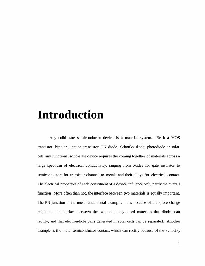
Figure I.1: Elements used in an integrated circuit , compiled from a survey of published literature [1-9]. Red: elements used in first integrated circuits, circa 1970. Blue: new elements incorporated in ICs, circa 2004. Orange: under research.
Early semiconductor devices and circuits involved few materials: silicon and its
natural oxide, a few dopant elements, and a few metals to make contacts and
interconnects. Today, integrated circuits involve many more elements in the periodic
table (figure I.1), and more exotic compounds to meet advanced performance and
reliability benchmarks, while being ever smaller. Examples include Ge for straining the
channel[1], HfO2 and ZrO2 for gate dielectric[2,3], Mo and its associated compounds
3
for gate[4], C in low-k interlayer dielectrics [5], W in vias[6], Co, Ni in silicides [7],
and As, Sb for low-diffusivity dopants. Many other elements and compounds, such as
PtSi[8], SrTiO[9], are also investigated as well.
As a result of this material “diversification”, interface properties are ever more
important, and start to impose limits on device design and performance. The
requirements for the interface between the gate dielectric and silicon complicate
considerably the material choice for high-k dielectric. In highly-scaled transistors, the
contact between highly doped source/drain and metal is the largest contributor of
parasitic resistance that lowers the drive current. Controlling short-channel effects
requires ever shallower and more abrupt junctions that are increasingly difficult to make
using existing process technologies.
As individual transistor shrinks in size, there is a growing interest in a new class
of one-dimensional semiconductor materials. These, represented by carbon nanotubes
and nanowires of various semiconductor materials, are synthesized using chemical and
self-assembly methods, and cannot be easily manufactured starting from bulk materials.
These nanowires and nanotubes offer new possibilities. In carbon nanotubes, for
example, carrier scattering is greatly reduced, leading to high carrier mobility, suitable
for high-perfomance transistors[10]. The mere shape of these nanotubes and nanowires
makes it easy to fabricate devices with new geometry, such as surround-gate transistors
with optimal electrostatic control[11].
4
The performance of these nanotube and nanowire transistors depends, just like
their counterpart in bulk, on proper engineering of the ir interfaces and junctions with
other materials. Semiconductor carbon nanotubes, for example, usually form Schottky
contacts with metals, and such a junction can dictate completely the device’s behavior
[12]. In Si nanowires, it has been shown that the conditions at the surface can alter the
carrier mobility considerably[13]. A similar behavior is observed in other type of
nanowire devices.
Unlike bulk materials, there are no systematic studies of the interfaces of these
bottom-up materials, with the exception of transport across CNT Schottky contacts.
The primary reason is the small size of these nano-objects, which precludes the usage of
common surface characterization techniques such as XPS, capacitance-voltage, DLTS,
admittance spectroscopy, or SIMS. Additionally, these nano-objects generally vary
greatly in size, and assembling many of them with a long-range order, in a way that
unambiguous information can be obtained, is still a challenge.
This thesis describes the investigation of some basic junctions in these novel
one-dimensional semiconductors using capacitance-voltage measurements, extended to
very low levels. Conventional instrumentation for this technique requires test
capacitors with an area in the order of 100µm x 100µm. As a result, this technique was
only applicable to bulk materials. In this work, this technique is extended to a much
higher precision in order to directly characterize an individual junction of small area.
The first application is to examine the dopant distribution in a VLS-grown silicon
5
nanowire and surface trap density at the interface between it and Al2O3 dielectric.
Second, the native surface of an InAs nanowire is examined. Third, a widely studied
junction, the metal-carbon nanotube Schottky junction, is re-examined to study its
impact on the performance of CNT transistors, and we further investigate this junction
in detail using the capacitance-voltage technique.
[1] C.-H. Jan et al., International Electron Device Meeting, December 2005,
Washington DC.
[2] M.A. Quevedo-Lopez et al., International Electron Device Meeting, December
2005, Washington DC.
[3] G.D. Wilk, R.M. Wallace, J.M. Anthony, J. Appl. Phys., 87, 484-492 (2000)
[4] P. Ranade, H. Takeuchi, T. King, C. Hu, Electrochemical and Solid State Letters, 4,
G85-G87 (2001)
[5] D. Shamiryan, F. Iacopi, S.H. Brongersma, Z.S. Yanovitskaya, J. Appl. Phys., 93,
8793 (2003)
[6] F. Liu et al, International Electron Device Meeting, December 2008, San Francisco.
[7] A. Lauwers et al, International Electron Device Meeting, December 2005,
Washington DC.
[8] J. Kedzierski, P. Xuan, E.H. Anderson, J. Bokor, T.J. King, C. Hu, International
Electron Device Meeting, December 2000, San Francisco.
[9] R.A. McKee, F.J. Walker, M.F. Chisholm, Phys. Rev. Lett., 81, 3014-3017 (1998)
[10] A. Javey, J. Guo, Q. Wang, M. Lundstrom, H. Dai, Nature, 424, 654-657 (2003)
[11] J. Goldberger, A. Hochbaum, R. Fan, P. Yang, Nano Lett., 6, 973-977 (2006)

6
[12] S. Heinze, J. Tersoff, R. Martel, V. Derycke, J. Appenzeller, P. Avouris, Phys. Rev.
Lett., 89, 106801 (2002)
[13] R. He and P. Yang, Nature Nanotechnology, 1, 42-46 (2006)

7
Chapter 1
Ultra Low-Level Capacitance Measurement
There are several related techniques for characterizing the electronic properties
of surfaces, interfaces and junctions in semiconductor materials. Probably the most
commonly used method is the capacitance-voltage (C-V) measurement. It is a versatile
and straightforward way of measuring simple parameters such as the static dielectric
constant e, and the effective dielectric thickness Tox. Frequency- and temperature-
dependent C-V measurements give information on interface trap density (Dit), and the
lifetime of these traps. When applied to a diffused junction or a Schottky junction, one
can extract material parameters such as the spatial distribution of dopants, as well as the
Schottky barrier height.

8
1.1 Requirements for the C-V measurement and the usual laboratory apparatus
The requirements for making good C-V measurements are very straightforward.
First, the C-V meter should be able to operate across a wide frequency range and to
resolve both capacitive and resistive components. Commercial C-V meters, usually
RLC analyzers, do this very well. Second, the test structure must be of sufficient size
and quality. A typical on-chip capacitor test structure needs to have an area of about
100µm x 100µm, to provide enough area for making contact with probe tips, and to
provide enough signal to be resolved by the C-V meter. In addition, the die lectric needs
to be insulating and robust enough to ensure low leakage, such that the resistive
component does not overwhelm the capacitive component, and that the dielectric does
not breakdown too easily during the measurement.
A commonly used RLC analyzer is the HP4284A, which applies an AC voltage
across the device under test (DUT) and measures the amplitude and phase of the current
through the DUT using a built- in ammeter. A circuit schematic (figure 1.1) from the
HP4284A operating manual shows the general working principle. Depending on the
chosen circuit model, the R,L,C parameters can be extracted. Unfortunately, the
HP4284A is limited by its poor current resolution (1nA) [1]. For an applied AC
amplitude of 25mV, the smallest impedance that can be resolved is about 25Mohm,
which translates to about 300aF at 20MHz. In practice, measurements are often
performed at much lower frequencies, and the resolution is significantly worse as a
result. Also, to obtain an accurate measurement, the applied AC amplitude can not be
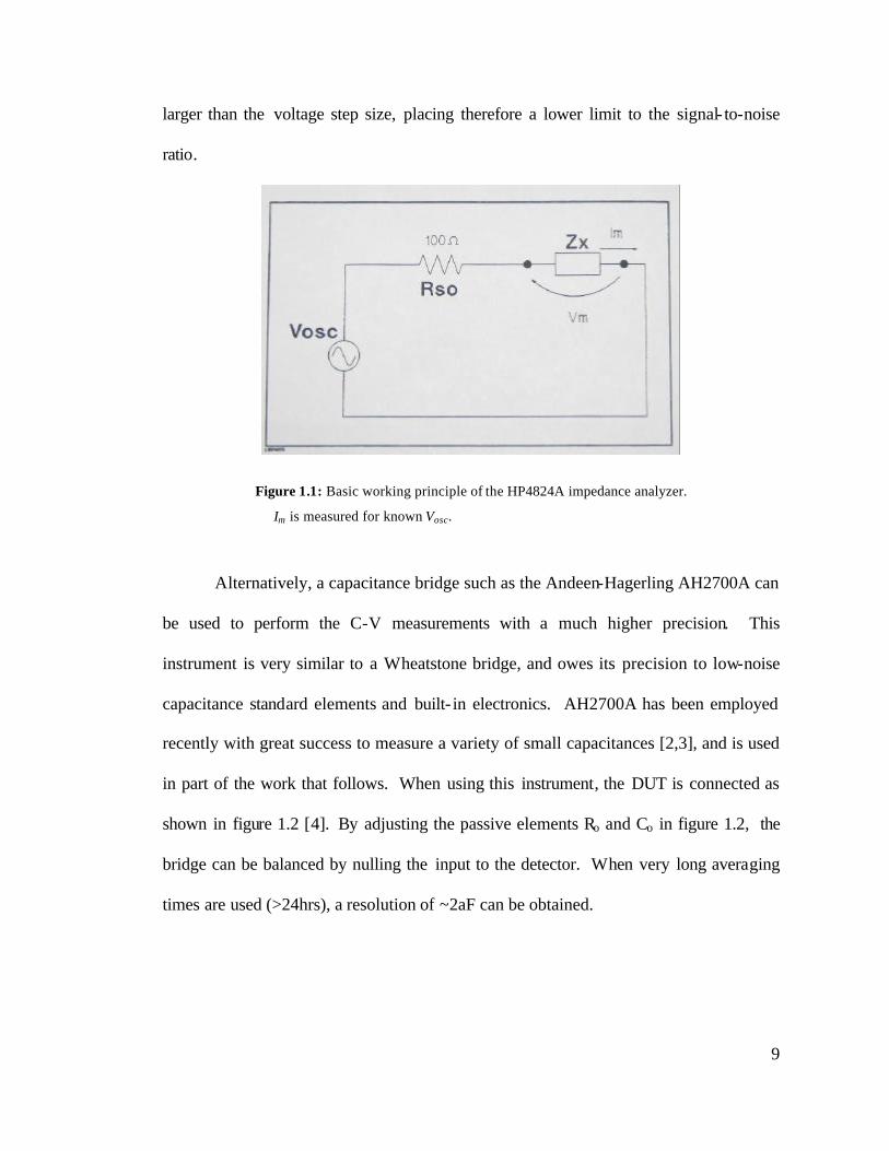
9
larger than the voltage step size, placing therefore a lower limit to the signal- to-noise
ratio.
Figure 1.1: Basic working principle of the HP4824A impedance analyzer.
Im is measured for known Vosc.
Alternatively, a capacitance bridge such as the Andeen-Hagerling AH2700A can
be used to perform the C-V measurements with a much higher precision. This
instrument is very similar to a Wheatstone bridge, and owes its precision to low-noise
capacitance standard elements and built- in electronics. AH2700A has been employed
recently with great success to measure a variety of small capacitances [2,3], and is used
in part of the work that follows. When using this instrument, the DUT is connected as
shown in figure 1.2 [4]. By adjusting the passive elements Ro and Co in figure 1.2, the
bridge can be balanced by nulling the input to the detector. When very long averaging
times are used (>24hrs), a resolution of ~2aF can be obtained.
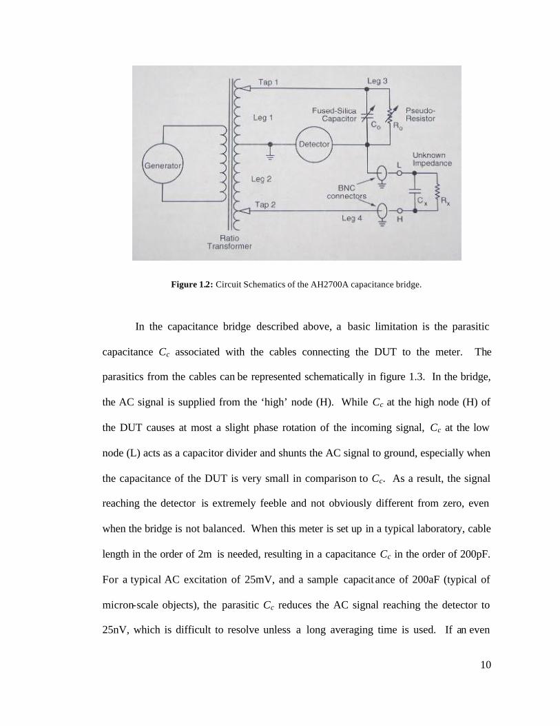
10
Figure 1.2: Circuit Schematics of the AH2700A capacitance bridge.
In the capacitance bridge described above, a basic limitation is the parasitic
capacitance Cc associated with the cables connecting the DUT to the meter. The
parasitics from the cables can be represented schematically in figure 1.3. In the bridge,
the AC signal is supplied from the ‘high’ node (H). While Cc at the high node (H) of
the DUT causes at most a slight phase rotation of the incoming signal, Cc at the low
node (L) acts as a capacitor divider and shunts the AC signal to ground, especially when
the capacitance of the DUT is very small in comparison to Cc. As a result, the signal
reaching the detector is extremely feeble and not obviously different from zero, even
when the bridge is not balanced. When this meter is set up in a typical laboratory, cable
length in the order of 2m is needed, resulting in a capacitance Cc in the order of 200pF.
For a typical AC excitation of 25mV, and a sample capacitance of 200aF (typical of
micron-scale objects), the parasitic Cc reduces the AC signal reaching the detector to
25nV, which is difficult to resolve unless a long averaging time is used. If an even
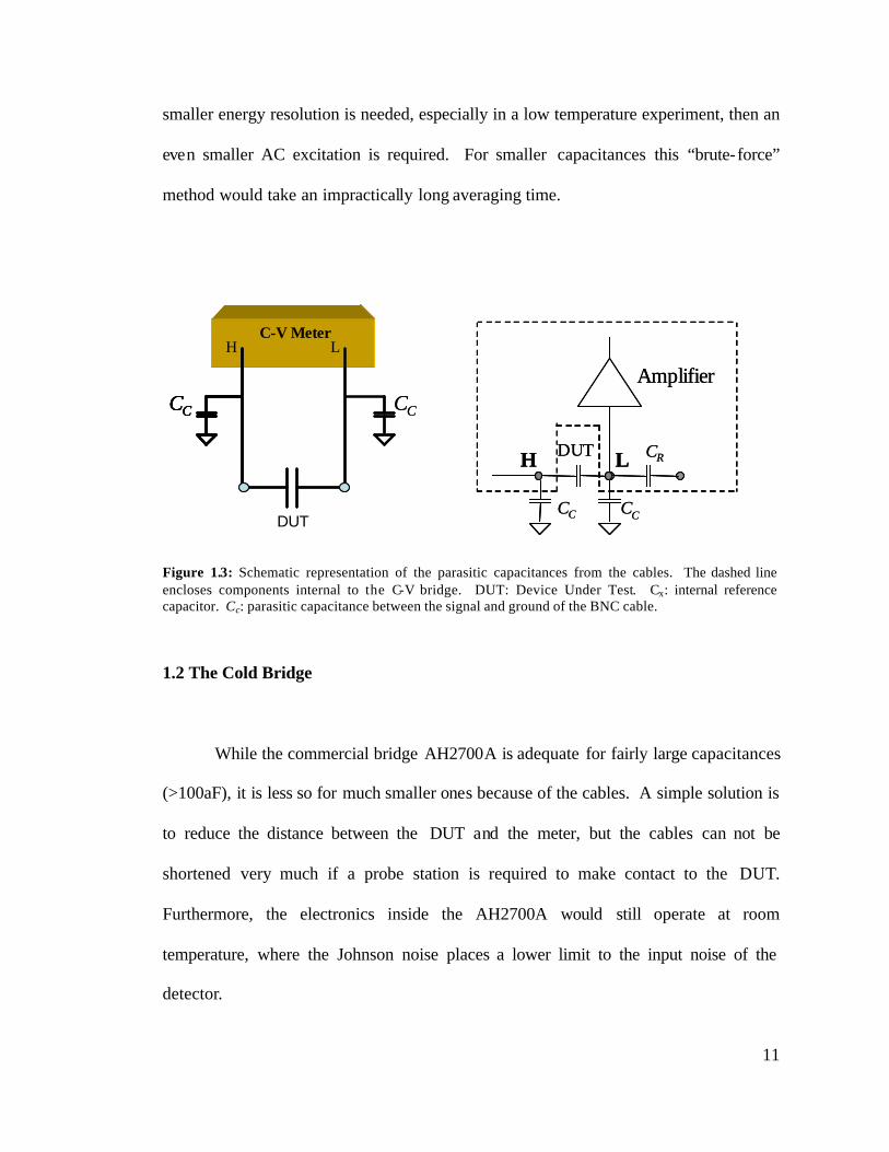
11
smaller energy resolution is needed, especially in a low temperature experiment, then an
even smaller AC excitation is required. For smaller capacitances this “brute-force”
method would take an impractically long averaging time.
H L
CC
C-V Meter
CC
H L
CC
C-V Meter
CCCCCC
DUT
H LDUT
CCCC
Amplifier
CRH LDUT
CCCC
Amplifier
CR
Figure 1.3: Schematic representation of the parasitic capacitances from the cables. The dashed line encloses components internal to the C-V bridge. DUT: Device Under Test. Cx: internal reference capacitor. Cc: parasitic capacitance between the signal and ground of the BNC cable.
1.2 The Cold Bridge
While the commercial bridge AH2700A is adequate for fairly large capacitances
(>100aF), it is less so for much smaller ones because of the cables. A simple solution is
to reduce the distance between the DUT and the meter, but the cables can not be
shortened very much if a probe station is required to make contact to the DUT.
Furthermore, the electronics inside the AH2700A would still operate at room
temperature, where the Johnson noise places a lower limit to the input noise of the
detector.
12
However, the basic improvements are clear: shorten the cables and operate at
low temperatures. Ashoori pioneered the use of ultra- low capacitance spectroscopy to
examine single electron charging in low-dimensional structures[5], by placing the
bridge on the same chip as the sample. Subsequent refinement by his group[6] consists
of mounting a similar apparatus on the tip of a scanning probe to perform spatially-
resolved capacitance spectroscopy. While impressive, the apparatus they developed
lacks the modularity that would allow the measurement of an arbitrary device. The
instrument described in this thesis allows one to apply this technique in a much more
general and flexible way to an arbitrary device.
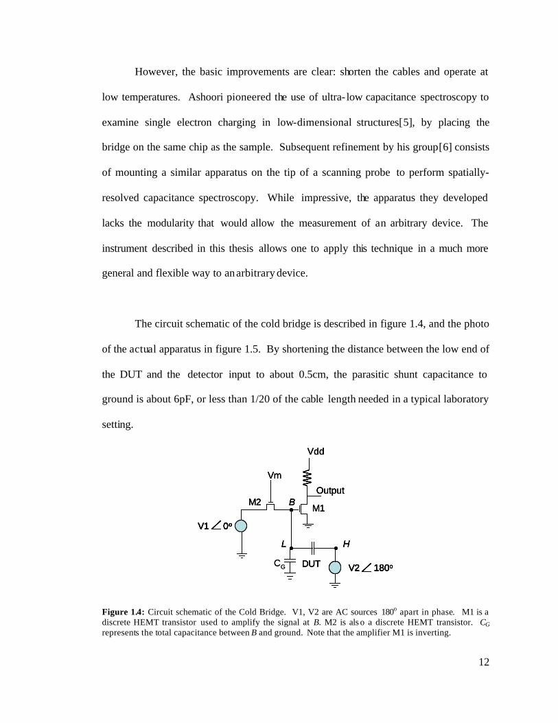
The circuit schematic of the cold bridge is described in figure 1.4, and the photo
of the actual apparatus in figure 1.5. By shortening the distance between the low end of
the DUT and the detector input to about 0.5cm, the parasitic shunt capacitance to
ground is about 6pF, or less than 1/20 of the cable length needed in a typical laboratory
setting.
Vm
M2Output
Vdd
M1
DUT
L H
B
180oV2
0oV1
CG
Vm
M2Output
Vdd
M1
DUT
L H
B
180oV2
0oV1
Vm
M2Output
Vdd
M1
DUT
L H
B
180oV2 180o180oV2
0oV1 0o0oV1
CG
Figure 1.4: Circuit schematic of the Cold Bridge. V1, V2 are AC sources 180o apart in phase. M1 is a discrete HEMT transistor used to amplify the signal at B. M2 is als o a discrete HEMT transistor. CG represents the total capacitance between B and ground. Note that the amplifier M1 is inverting.

13
Figure 1.5: Photo of the actual Cold Bridge.
1.3 Operating the Cold Bridge
To measure capacitances with the cold bridge, one balances the bridge so that
voltage at the balance point ‘B’ illustrated in figure 1.4 is minimized (to zero in theory),
by varying the amplitude of one of the AC sources (V1, V2). These two AC sources are
180o apart in phase so their contribution subtract from each another. The voltage at the
balance point B is simply:
++
−
++
=DUTGR
DUT
DUTGR
RB CCC
CV
CCCC
VV 21 (1.1)
, where the negative sign is due to the out-of-phase V2. When balanced, VB=0, and the
numerical value of the capacitance can then be extracted using this simple formula:
DUTR CVCV 21 = (1.2)
14
, where CR, CG, CDUT are respectively the capacitor representing the reference, parasitics
to ground and device under test. When biased by VM to be almost completely off, the
discrete HEMT transistor (M2) serves as the reference capacitor CR. This scheme has
the added advantage that a separate high-resistance DC path to bias the amplifier M1 is
unnecessary. In fact, the presence of that high resistance DC path, in the form of a large
resistor, would be detrimental to the signal-to-noise ratio since it further reduces the
incoming AC signal by shunting it to ground, and acts as a significant noise source for
M1. The voltage-adjustable M2 provides a convenient way to bias M1 and acts as a
reference capacitor simultaneously. An added bonus is that, by turning on M2, I-V
characterization of the DUT can be performed in-situ, without having to remove the
device from the setup. The precise value of CR can be measured it using the AH2700A
commercial bridge, and is 0.37pF in our case.
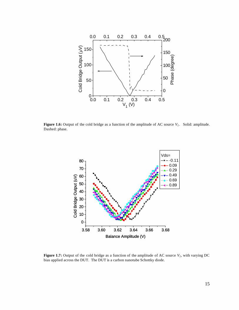
A typical balancing curve is shown in figure 1.6. It is simply the output of the
bridge as a function of the amplitude of V1 (see figure 1.4). As expected, the bridge
goes through a minimum (the balance point), accompanied by an abrupt change in the
phase from 0 to 180 degree, evidence that contribution from AC source V1 has become
larger. In all devices of interest in this work, the capacitance of the DUT changes with
bias applied across it. When this happens, we should expect the balance curve to
simply shift horizontally with applied bias, as illustrated in figure 1.7.
15
0.0 0.1 0.2 0.3 0.4 0.50
50
100
150
Pha
se (d
egre
e)
Col
d B
ridge
Out
put (
µV)
V1 (V)
0.0 0.1 0.2 0.3 0.4 0.5
0
50
100
150
200
Figure 1.6: Output of the cold bridge as a function of the amplitude of AC source V1. Solid: amplitude. Dashed: phase.
3.58 3.60 3.62 3.64 3.66 3.68
0
10
20
30
40
50
60
70
80
Col
d B
ridge
Out
put (
uV)
Balance Amplitude (V)
Vds= -0.11 0.09 0.29 0.49 0.69 0.89
3.58 3.60 3.62 3.64 3.66 3.68
0
10
20
30
40
50
60
70
80
Col
d B
ridge
Out
put (
uV)
Balance Amplitude (V)
Vds= -0.11 0.09 0.29 0.49 0.69 0.89
Figure 1.7: Output of the cold bridge as a function of the amplitude of AC source V1, with varying DC bias applied across the DUT. The DUT is a carbon nanotube Schottky diode.
16
1.4 Full setup
The full measurement setup outside of the cold bridge is described below for
future reference. First, the phase between the two AC sources is carefully trimmed to
be as close to 180o apart as possible. The instruments used for the AC sources are the
internal sine generator of the SR830 lock- in amplifier and the HP3312A function
generator, whose phase can be adjusted relative to an external trigger. This phase
adjustment is necessary to ensure that the bridge output is as small as possible when
balanced, and that the simple formula 1.2 can be applied to extract the capacitance of
the DUT. Also, as obvious from figure 1.4, the DC bias applied across the DUT for C-
V measurement needs to be added to V2, and another DC voltage is needed to bias the
transistor M1, and should be added to V1. The addition of the AC source to the DC
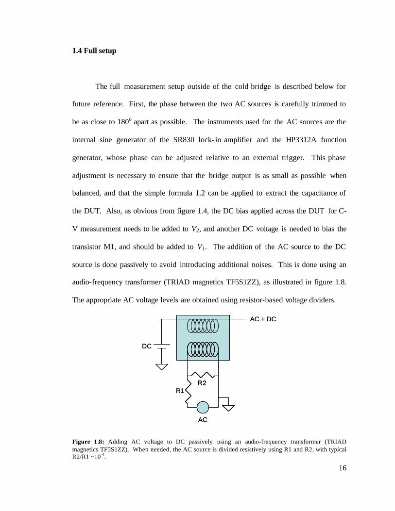
source is done passively to avoid introducing additional noises. This is done using an
audio-frequency transformer (TRIAD magnetics TF5S1ZZ), as illustrated in figure 1.8.
The appropriate AC voltage levels are obtained using resistor-based voltage dividers.
R1R2
AC
DC
AC + DC
R1R2
AC
DC
AC + DC
Figure 1.8: Adding AC voltage to DC passively using an audio-frequency transformer (TRIAD magnetics TF5S1ZZ). When needed, the AC source is divided resistively using R1 and R2, with typical R2/R1 ~10-4.

17
1.5 Noise Performance of the Cold Bridge
With all components of the bridge optimized and using a lock- in amplifier to
reject unwanted noise, the bridge has a noise figure of about 0.3 electrons / Hz1/2 at
77K. Using a typical AC excitation of 20mV and an averaging time of about 120s per
data point, the noise figure translates into a capacitance resolution ?C of:
VoltageACBandwidthEffectiveFigureNoiseC ××=∆ (1.3)
aFmVHze
C 4.120120/13.0 =××=∆ (1.4)
With a larger AC excitation or greater patience, the bridge can easily resolve
capacitances lower than 1 aF.
The capability to measure small capacitances allows for the characterization of
individual nanoscale semiconductor devices. As an example, the dimensions of an end-
of-the-roadmap silicon MOSFET [7], Lg = W=8.8nm and EOT = 0.5nm, lead to a
capacitance of ~5.3 aF, well within the capability of the instrument described above.
1.6 Device layout and design to minimize background capacitance
Although the cold bridge is designed to accept an arbitrary device, there are
restrictions to the device layout. Illustrated in figure 1.9 are the various parasitic
18
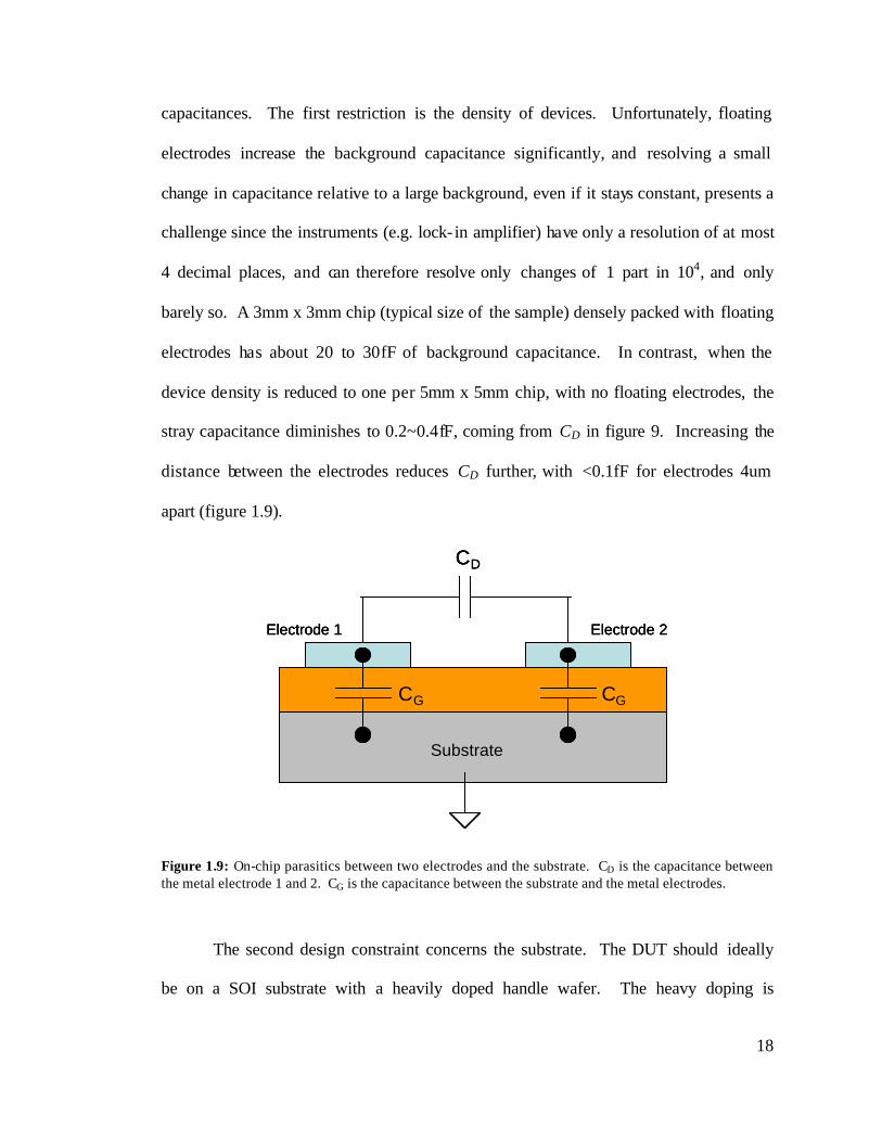
capacitances. The first restriction is the density of devices. Unfortunately, floating
electrodes increase the background capacitance significantly, and resolving a small
change in capacitance relative to a large background, even if it stays constant, presents a
challenge since the instruments (e.g. lock- in amplifier) have only a resolution of at most
4 decimal places, and can therefore resolve only changes of 1 part in 104, and only
barely so. A 3mm x 3mm chip (typical size of the sample) densely packed with floating
electrodes has about 20 to 30fF of background capacitance. In contrast, when the
device density is reduced to one per 5mm x 5mm chip, with no floating electrodes, the
stray capacitance diminishes to 0.2~0.4fF, coming from CD in figure 9. Increasing the
distance between the electrodes reduces CD further, with <0.1fF for electrodes 4um
apart (figure 1.9).
CG CG
CD
Electrode 1 Electrode 2
Substrate
CG CG
CD
Electrode 1 Electrode 2
CG CG
CD
Electrode 1 Electrode 2
Substrate
Figure 1.9: On-chip parasitics between two electrodes and the substrate. CD is the capacitance between the metal electrode 1 and 2. CG is the capacitance between the substrate and the metal electrodes.
The second design constraint concerns the substrate. The DUT should ideally
be on a SOI substrate with a heavily doped handle wafer. The heavy doping is
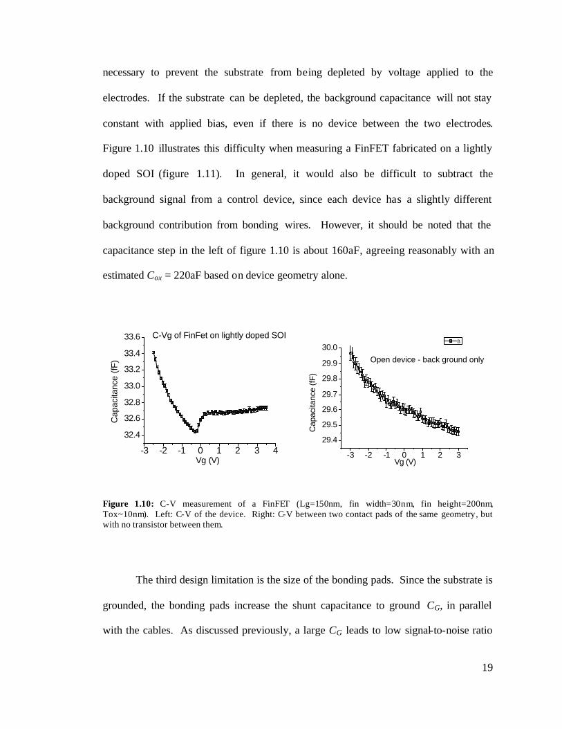
19
necessary to prevent the substrate from being depleted by voltage applied to the
electrodes. If the substrate can be depleted, the background capacitance will not stay
constant with applied bias, even if there is no device between the two electrodes.
Figure 1.10 illustrates this difficulty when measuring a FinFET fabricated on a lightly
doped SOI (figure 1.11). In general, it would also be difficult to subtract the
background signal from a control device, since each device has a slightly different
background contribution from bonding wires. However, it should be noted that the
capacitance step in the left of figure 1.10 is about 160aF, agreeing reasonably with an
estimated Cox = 220aF based on device geometry alone.
-3 -2 -1 0 1 2 3 4
32.4
32.6
32.8
33.0
33.2
33.4
33.6 C-Vg of FinFet on lightly doped SOI
Cap
acita
nce
(fF)
Vg (V)
-3 -2 -1 0 1 2 3
29.4
29.5
29.6
29.7
29.8
29.9
30.0
Cap
acita
nce
(fF)
Vg (V)
B
Open device - back ground only
Figure 1.10: C-V measurement of a FinFET (Lg=150nm, fin width=30nm, fin height=200nm, Tox~10nm). Left: C-V of the device. Right: C-V between two contact pads of the same geometry, but with no transistor between them.
The third design limitation is the size of the bonding pads. Since the substrate is
grounded, the bonding pads increase the shunt capacitance to ground CG, in parallel
with the cables. As discussed previously, a large CG leads to low signal-to-noise ratio

20
and reduces resolution. A typical bonding pad is a 75µm x 75µm square on an oxide
layer 500nm in thickness, giving a tolerable CG = 0.38pF. When these design
limitations are satisfied, the background capacitance is constant to better than 2aF,
within the error bars, as illustrated in figure 1.12.
Figure 1.11: SEM image of the FinFET measured in figure 1.10. Capacitance is measured between the gate (top right), and the source/drain electrodes (upper left and lower right), which are shorted together.
-10 -5 0 5 10
346
348
350
352
354
Cap
acita
nce
(aF
)
Substrate Bias (V)

21
Figure 1.12: Capacitance between two metal electrodes 1µm apart, as function of the substrate bias. No device exists between the electrodes. The substrate is heavily doped with boron to at least 1019/cm3.
1.7 Dealing with losses
When measuring small capacitances, even a seemingly large resistive
component in parallel of the capacitor can make the loss unmanageable. Lossy
capacitors are encountered in very thin or leaky dielectrics, heavily doped junctions, and
Schottky diodes. As an estimate, for C=100aF measured at 10kHz, a resistance of 160
GOhm is sufficient to produce a loss tangent of 1, making the simple formula 1.2
unapplicable. Instead, a more complicated circuit model that includes the resistor in
parallel must be used (figure 1.13) and the capacitance extracted using linear circuit
analysis.
CDUT
RDUT
CRV1 V2
Balance point
CG
CDUT
RDUT
CRV1 V2
Balance pointCDUT
RDUT
CRV1 V2
Balance point
CG
Figure 1.13: Parallel model for lossy capacitor. The loss is modeled by the resistor RDUT in parallel with the capacitor.
Linear circuit theory gives the voltage VB simply as:
22
−
=
t
R
t
DUTB Y
YV
YY
VV 21 (1.5)
Where Yx = 1/Zx is the admittance between any node x to node B in figure 1.13, and Yt is
the sum of the admittances joining the balance point and the other three nodes. Further
simplification gives the real and imaginary parts separately:
( )2111
VCVCCj
jRV
CjV RDUT
GDUTGB −+
=
ωω
ω (1.6)
)(
/
21
1
VCVCRV
VRDUT
DUTB −
=∠ω
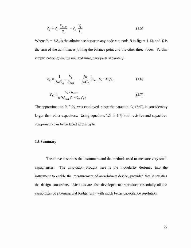
(1.7)
The approximation Yt ˜ YG was employed, since the parasitic CG (6pF) is considerably
larger than other capacitors. Using equations 1.5 to 1.7, both resistive and capacitive
components can be deduced in principle.
1.8 Summary
The above describes the instrument and the methods used to measure very small
capacitances. The innovation brought here is the modularity designed into the
instrument to enable the measurement of an arbitrary device, provided that it satisfies
the design constraints. Methods are also developed to reproduce essentially all the
capabilities of a commercial bridge, only with much better capacitance resolution.
23
References
[1] HP4284A Operation Manual [2] S. Ilani, L.A.K. Donev, M. Kindermann, P.L. McEuen, Nature Physics, 2, 687-691
(2006).
[3] R. Tu, L. Zhang, Y. Nishi, H. Dai, Nano Letters, 7, 1561-1565 (2007).
[4] AH2700A Operation manual [5] R.C. Ashoori, H.L. Stormer, J.S. Weiner, L.N. Pfeiffer, S.J. Pearton, K.W. Baldwin,
K.W. West, Phys. Rev. Lett., 68, 3088-3091 (1992).
[6] Gary Steele, Ph.D. Thesis, Massachusetts Institute of Technology (2006).
[7] ITRS Roadmap 2008, www.itrs.net

24

25
Chapter 2
Diffused junction in a silicon nanowire
Semiconductor nanowires are useful in several applications, including
biochemical sensing, computing and energy harvesting[1,2,3,4,5]. However, important
material parameters such as the dopant distribution and surface state density have not
been measured in nanowires. Here, C-V method is applied directly to a single silicon
nanowire surround gate field effect transistor to extract the radial dopant distribution
and interface state density. The methods previously used [6] to determine the dopant
density rely on several untested assumptions that can lead to very large uncertainties.
For example, the dopant concentration is typically extracted by making nanowire field
effect transistors (FETs) and using the conductivity in conjunction with the measured
26
mobility and threshold voltage[7,8,9]. These methods rely on the calculated gate
capacitance and assume a uniform dopant distribution and known surface (or interface)
charge density. In planar devices, the above assumptions can be tested using the
capacitance-voltage (C-V) technique[10], and the same method is applied here to a
nanowire device.
Previous reports on direct C-V measurements on nanowires exist, but these are
concerned with measuring the oxide capacitance for the purpose of mobility
extraction[11,12]. Accurate mobility measurements are important, and a similar study
performed on individual InAs nanowires is presented in the next chapter. A recent
study of InAs nanowires addresses the issue of interface trap density, but it was
performed on a large ensemble of wires having a large size distribution, and
inconsistent electrical contacts[13].
The work presented in this chapter demonstrates the application of C-V
measurements on a silicon nanowire transistor, fabricated using a bottom-up method.
The interface state density Dit as a function of the energy position inside the bandgap is
extracted with the high- low method and the radial dopant profile is determined from
high frequency C-V measurement. Finite element modeling (FEM) is used to support
the results and to show the limitations in resolving the dopant profile using the C-V
method. The results are also compared with those from planar metal oxide
semiconductor capacitors.

27
2.1 Design of test structure and measurement scheme
The test structure is similar to that proposed by Ilani et al[14]. Figure 2.1
illustrates the design of the structure. On an SOI wafer, a silicon nanowire bridges two
heavily boron-doped silicon pads (S and D), about 4µm apart. A high-k/metal gate
stack surrounding the nanowire acts as the top gate. This gate stack, in series with the
nanowire, effectively forms a MOS capacitor (MOSCAP). However, 1µm of the
nanowire from the source and the drain electrode is not covered by the top gate, and is
instead gated by the back gate (BG). The back gate is used to extract the background
parasitic capacitances.
S
D
G
BG
S
D
G
BG
S
D
G
BG
Figure 2.1 Device test structure for CV measurement. S/D: source and drain. G: top gate. BG: back gate. The cross section shows the wire under the top gate. A thin layer of aluminum oxide separates the nanowire channel from the top gate electrode. Credit: E.Garnett.

28
Capacitance is measured between the top gate and the source/drain electrodes,
the latter two shorted together. In the first measurement, the back gate is negatively
biased to turn on the exposed parts of the nanowire, and both the MOSCAP and the
background parasitics contribute to the measured capacitance. In the second
measurement, a large positive voltage applied to the back gate turns off the exposed
parts of the nanowire, and the nanowire MOSCAP is not measured. The difference
between these two measurements yield only the capacitance from the nanowire
MOSCAP. The measurement scheme is illustrated in figure 2.2.
S DTop Gate
Back Gate
CS
CP CP
-20V
S DTop Gate
Back Gate
CS
CP CP
S DTop Gate
Back Gate
CS
CP CP
-20V
S D
Top Gate
Back Gate
CP CP
CS
+8V
S D
Top Gate
Back Gate
CP CP
CS
S D
Top Gate
Back Gate
CP CP
CS
+8V
Figure 2.2 Measuring scheme to extract background capacitance. Left: Negatively biased back gate leads to low resistance contact to the MOSCAP. Right: positively biased back gate turns off access the the nanowire MOSCAP.
2.2 Device fabrication
Starting with (110) SOI wafers with heavily doped handle and device layers,
standard microfabrication techniques are used to define silicon islands that serve as the
source/drain electrodes. Gold nanoparticles with an average diameter of 80nm are then
dispersed from solution onto the silicon islands. Vapor-liquid-solid growth of the
nanowires at 830oC follows, catalyzed by the gold nanoparticles[15,16]. The silicon

29
precursor is liquid SiCl4 kept at 0oC, bubbled into the furnace using a mixture of Ar and
H2 (50 and 158sccm, respectively). Since the growth is epitaxial, the long axis of the
nanowires are generally perpendicular to the (111) planes of the silicon surface. It
should be noted that the islands are aligned such that the direction the nanowires are
expected to bridge is parallel to the (111) directions. A (110) wafer is used because it
can be patterned such that the (111) surfaces are exposed, and that the (111) directions,
to which the nanowires align, are in the plane of the wafer [17].
The nanowires are then doped with boron by annealing for 1 hour at 675 oC with
500 sccm of carrier gas and 0.5 sccm of 1% BCl3 in Ar, followed by 15 minutes at the
same temperature with the BCl3 line turned off. Using these process conditions, a
dopant profile can be simulated using Tsupreme, a commercial semiconductor process
simulation tool. The expected dopant profile is shown as the dark solid line in figure
2.9 (Na-diffusion). The Al2O3 gate dielectric is deposited in a ALD chamber using
alternating pulses of trimethylaluminum and water precursors. The surround gate metal
is patterned via photolithography and chromium sputtering, followed by lift-off.
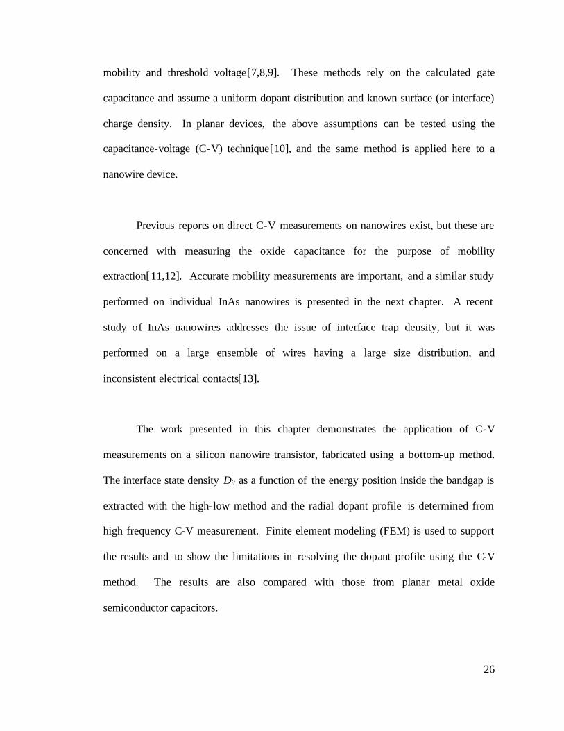
Figure 2.3 shows a completed Si nanowire FET. After all measurements of
interest are performed, focused ion beam (FIB) milling is used to expose the buried part
of the wire in order to measure the actual diameter. The wire appears to be fully
embedded in the surround gate metal and epitaxially integrated into the silicon
electrodes. The cross-sectional SEM shows a distinct contrast between the bright Cr
surround gate and the dark Al2O3 gate oxide, with a somewhat smaller contrast
30
difference at the Si/Al2O3 interface. The cross-sectional and top view SEM images
show a gate length of 2.3 microns, Si nanowire diameter of about 75 nm and Al2O3
thickness of about 15 nm. The thickness of the Al2O3 is consistent across a large (cm2)
area, and with a TEM measurement on control samples.
S
D
G
S
D
G
Figure 2.3 SEM picture of an actual nanowire device. The inset is a cross-sectional view of the device taken after focused ion beam (FIB) mi lling. The scale bars are 1 µm (main panel) and 100 nm (inset). Credit: M. Fardy.
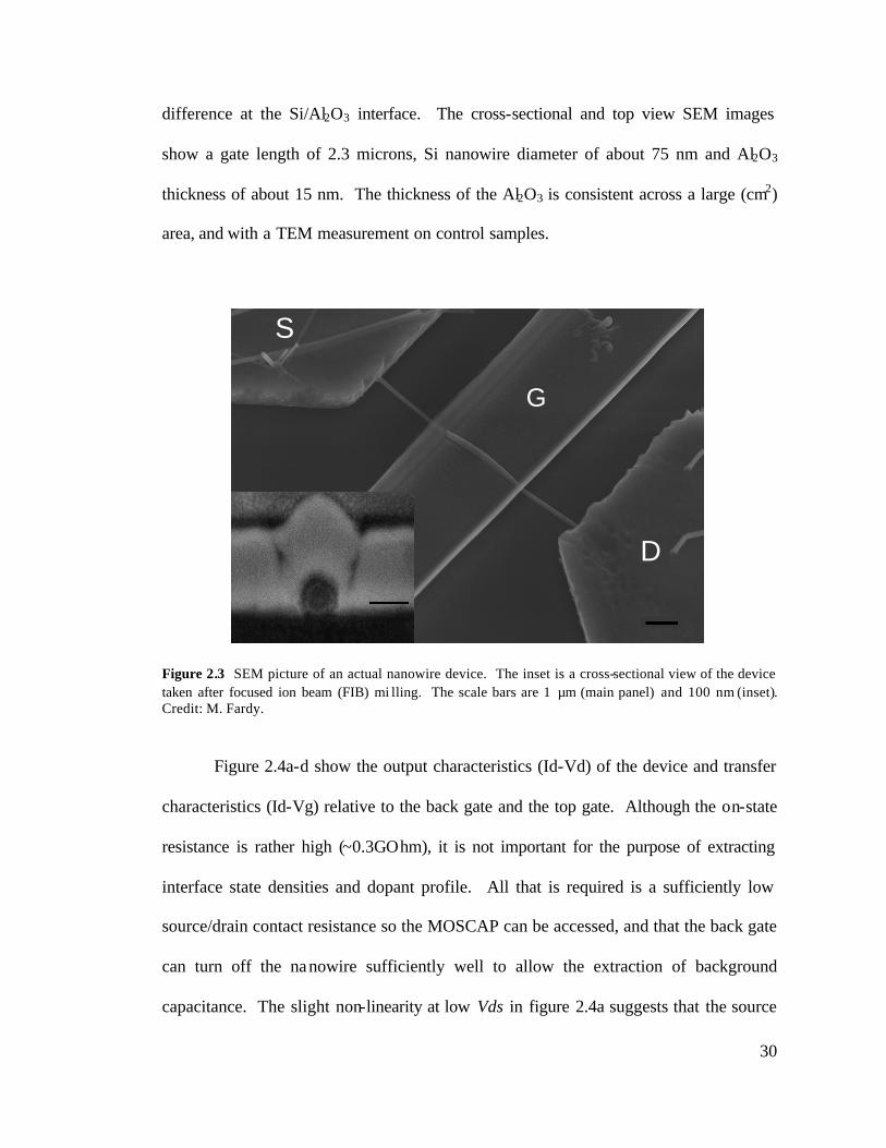
Figure 2.4a-d show the output characteristics (Id-Vd) of the device and transfer
characteristics (Id-Vg) relative to the back gate and the top gate. Although the on-state
resistance is rather high (~0.3GOhm), it is not important for the purpose of extracting
interface state densities and dopant profile. All that is required is a sufficiently low
source/drain contact resistance so the MOSCAP can be accessed, and that the back gate
can turn off the nanowire sufficiently well to allow the extraction of background
capacitance. The slight non-linearity at low Vds in figure 2.4a suggests that the source
31
or drain contact may be a Schottky contact, possibly because of residual oxide on the
surface of the trench sidewall. It should also be noted that there is very little hysteresis
in figure 2.4b, despite the application of very large voltages. This suggests that the
effect of bias-induced stress and charge injection from the gates are very small.
-1.0 -0.5 0.0 0.5 1.0
-4
-3-2-1
012
34 a)
Top Gate fixed at -2V
1V-6V-13V
Back Gate = -20V
Dra
in c
urre
nt (
nA)
Vds (V)
-20 -15 -10 -5 0 5 101E-3
0.01
0.1
1
10
100
Top Gate fixed at -2V
b)Vds = 0.1V
Dra
in C
urre
nt (
pA)
Back Gate (V)
-1.0 -0.5 0.0 0.5 1.0
-4-3-2-101234
2V to 6V
0V
C) Top Gate = -2V
Back Gate fixed at -20V
Dra
in C
urre
nt (
nA)
Vds (V)
-2 0 2 4 61E-3
0.01
0.1
1
10
100d)
Back gate fixed at -20V
Dra
in C
urre
nt (p
A)
Top Gate (V)
Vds=20mV Vds=100mV
Figure 2.4 a) Output characteristics (Id-Vd) of the device in figure 2.3 as a function of the back gate. The top gate is fixed at -2V. b) Transfer (Id-Vg) characteristics, vs the back gate, of the Si NW transistor shown in figure 2.3. c) Id -Vd for various top gate voltage. The back gate was -20V. d) Id-Vg characteristics, vs the top gate.
32
2.3 The capacitance measurement
Since the furnace for growing the nanowires accommodates only substrates no
wider than 1”, it is necessary to have a large device density on each chip to obtain a
usable number of devices. On a single test chip, there can be more than 100 silicon
islands, leading to a large parasitic background capacitance of about 20fF.
Nevertheless, the measurement method is precise to less than 10aF, and the large
background only presents a minor inconvenience. Electrical contacts are made to the
source, drain and gate electrodes by wirebonding from a ceramic package to the
degenerately boron-doped silicon source and drain pads and the chromium surround
gate. Appropriate ultrasonic power is used to break through the Al2O3 layer covering
the source and drain. The series resistances from these wirebonds are negligible
compared to that of the nanowire.
Following the scheme in figure 2.2, the capacitance is measured using the
Andeen-Hagerling AH2700A with an AC amplitude of 20 mV at 77K, with sufficiently
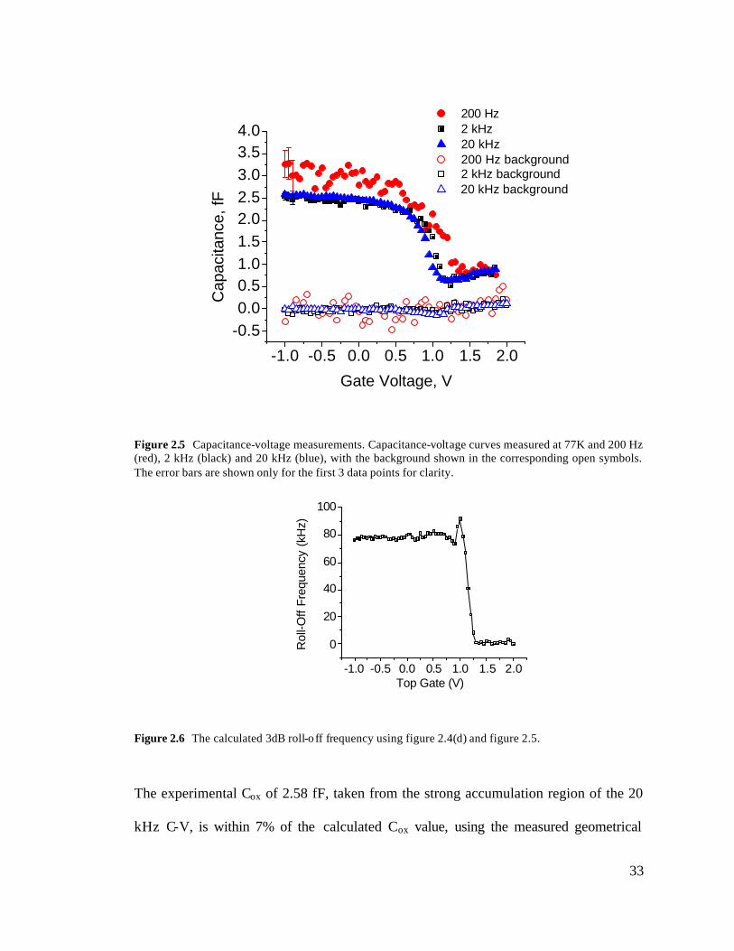
long averaging times. Figure 2.5 shows the silicon nanowire C-V response at 200 Hz, 2
kHz and 20 kHz with the back gate set at -20 V. The background capacitance is
measured with the back gate set at +8 V. Both measurements are repeated at the 3
frequencies. The C-V curves clearly show the expected accumulation and depletion
regions. At larger positive gate biases (not shown), inversion does seem to occur, but
the data in that regime is not expected to be accurate since the contact to the wire is p-
type, and the access resistance to a n-type inversion layer would be a large one.
33
-1.0 -0.5 0.0 0.5 1.0 1.5 2.0
-0.50.00.51.01.52.02.53.03.54.0
Cap
acita
nce,
fF
Gate Voltage, V
200 Hz 2 kHz 20 kHz 200 Hz background 2 kHz background 20 kHz background
Figure 2.5 Capacitance-voltage measurements. Capacitance-voltage curves measured at 77K and 200 Hz (red), 2 kHz (black) and 20 kHz (blue), with the background shown in the corresponding open symbols. The error bars are shown only for the first 3 data points for clarity.
-1.0 -0.5 0.0 0.5 1.0 1.5 2.0
0
20
40
60
80
100
Rol
l-Off
Freq
uenc
y (k
Hz)
Top Gate (V)
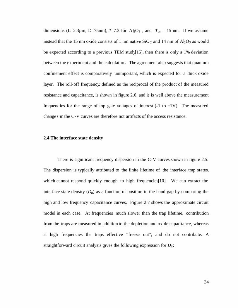
Figure 2.6 The calculated 3dB roll-o ff frequency using figure 2.4(d) and figure 2.5.
The experimental Cox of 2.58 fF, taken from the strong accumulation region of the 20
kHz C-V, is within 7% of the calculated Cox value, using the measured geometrical
34
dimensions (L=2.3µm, D=75nm), ?=7.3 for Al2O3 , and Tox = 15 nm. If we assume
instead that the 15 nm oxide consists of 1 nm native SiO 2 and 14 nm of Al2O3 as would
be expected according to a previous TEM study[15], then there is only a 1% deviation
between the experiment and the calculation. The agreement also suggests that quantum
confinement effect is comparatively unimportant, which is expected for a thick oxide
layer. The roll-off frequency, defined as the reciprocal of the product of the measured
resistance and capacitance, is shown in figure 2.6, and it is well above the measurement
frequencies for the range of top gate voltages of interest (-1 to +1V). The measured
changes in the C-V curves are therefore not artifacts of the access resistance.
2.4 The interface state density
There is significant frequency dispersion in the C-V curves shown in figure 2.5.
The dispersion is typically attributed to the finite lifetime of the interface trap states,
which cannot respond quickly enough to high frequencies[10]. We can extract the
interface state density (Dit) as a function of position in the band gap by comparing the
high and low frequency capacitance curves. Figure 2.7 shows the approximate circuit
model in each case. At frequencies much slower than the trap lifetime, contribution
from the traps are measured in addition to the depletion and oxide capacitance, whereas
at high frequencies the traps effective “freeze out”, and do not contribute. A
straightforward circuit analysis gives the following expression for Dit:
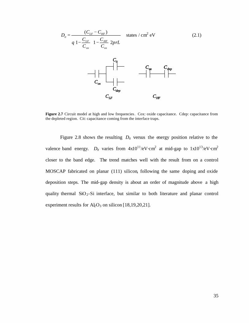
35
Dit =(CLF − CHF )
q 1−CLF
Cox
1−
CHF
Cox
2πrL
states / cm2 eV (2.1)
CHF
Cox Cdep
CLF
Cit
Cox
Cdep
CHF
Cox Cdep
CHF
Cox CdepCox Cdep
CLF
Cit
Cox
Cdep
CLF
Cit
Cox
Cdep
Figure 2.7 Circuit model at high and low frequencies. Cox: oxide capacitance. Cdep: capacitance from the depleted region. Cit: capacitance coming from the interface traps.
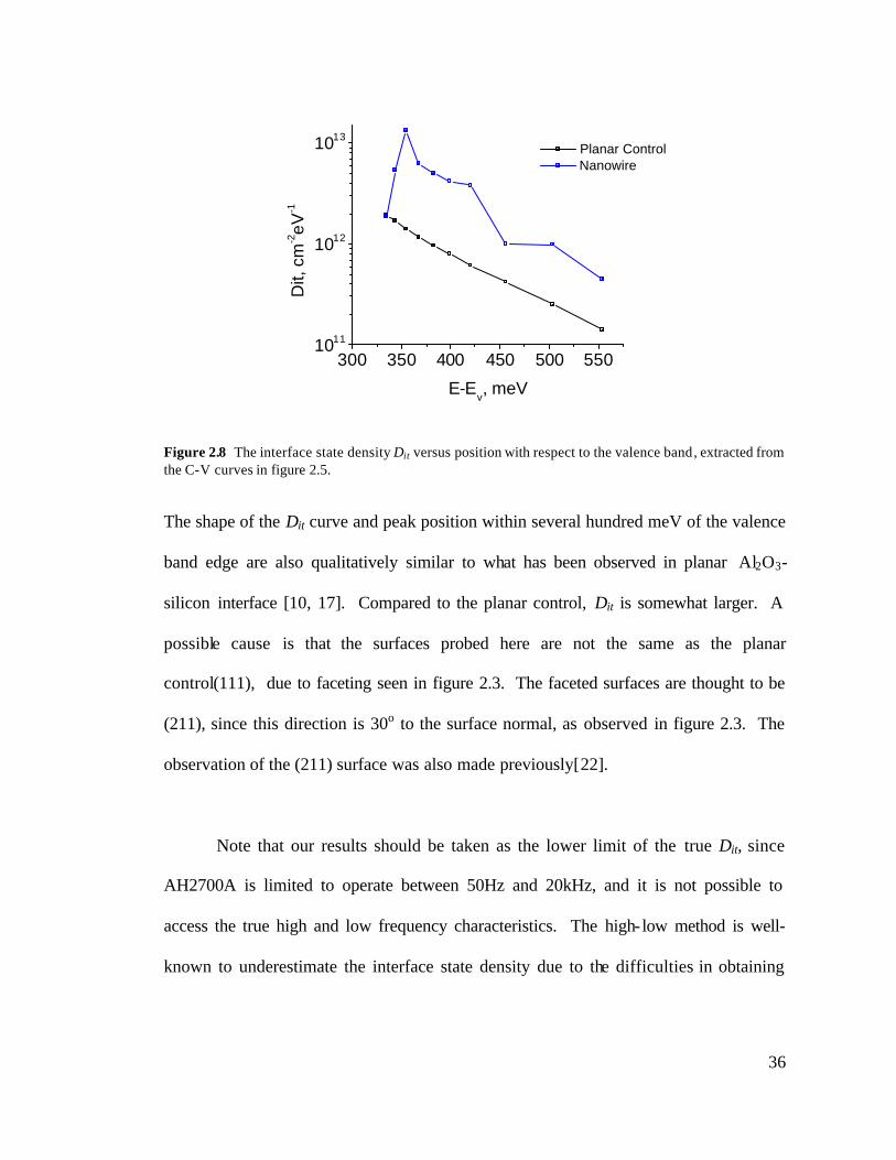
Figure 2.8 shows the resulting Dit versus the energy position relative to the
valence band energy. Dit varies from 4x10¹¹/eV·cm2 at mid-gap to 1x10¹³/eV·cm2
closer to the band edge. The trend matches well with the result from on a control
MOSCAP fabricated on planar (111) silicon, following the same doping and oxide
deposition steps. The mid-gap density is about an order of magnitude above a high
quality thermal SiO2-Si interface, but similar to both literature and planar control
experiment results for Al2O3 on silicon [18,19,20,21].
36
300 350 400 450 500 5501011
1012
1013
Dit,
cm
-2eV
-1
E-Ev, meV
Planar Control Nanowire
Figure 2.8 The interface state density Dit versus position with respect to the valence band, extracted from the C-V curves in figure 2.5.
The shape of the Dit curve and peak position within several hundred meV of the valence
band edge are also qualitatively similar to what has been observed in planar Al2O3-
silicon interface [10, 17]. Compared to the planar control, Dit is somewhat larger. A
possible cause is that the surfaces probed here are not the same as the planar
control(111), due to faceting seen in figure 2.3. The faceted surfaces are thought to be
(211), since this direction is 30o to the surface normal, as observed in figure 2.3. The
observation of the (211) surface was also made previously[22].
Note that our results should be taken as the lower limit of the true Dit, since
AH2700A is limited to operate between 50Hz and 20kHz, and it is not possible to
access the true high and low frequency characteristics. The high- low method is well-
known to underestimate the interface state density due to the difficulties in obtaining
37
true high and low frequency behavior. However, from previous studies on planar
silicon we expect a difference no more than a factor of two from the true profile[10, 23].
2.5 Dopant profile
We have also extracted the dopant profile using the high frequency C-V curve,
using depletion approximation. The results are compared to the simulation from a
commercial semiconductor process simulator, TSupreme, using the actual device
dimensions and process conditions, including the interstitial- and vacancy-assisted
diffusion models. In addition, we assume that the dopant concentration at the surface is
fixed at the solid solubility (2x10¹⁹/cm3 at 675oC). The depletion approximation is also
verified using finite element electrostatic simulations (COMSOL Multiphysics), to
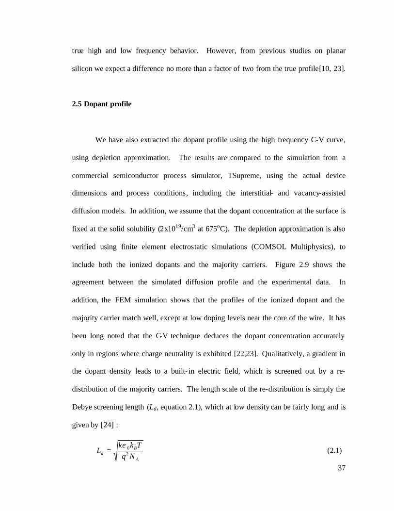
include both the ionized dopants and the majority carriers. Figure 2.9 shows the
agreement between the simulated diffusion profile and the experimental data. In
addition, the FEM simulation shows that the profiles of the ionized dopant and the
majority carrier match well, except at low doping levels near the core of the wire. It has
been long noted that the C-V technique deduces the dopant concentration accurately
only in regions where charge neutrality is exhibited [22,23]. Qualitatively, a gradient in
the dopant density leads to a built- in electric field, which is screened out by a re-
distribution of the majority carriers. The length scale of the re-distribution is simply the
Debye screening length (Ld, equation 2.1), which at low density can be fairly long and is
given by [24] :
A
Bd Nq
TkL 2
0κε= (2.1)
38
0 5 10 15 20 25 30 35 401015
1016
1017
1018
1019
Dop
ant C
once
ntra
tion,
cm
-3
Distance from center, nm
p(r) - diffusion p(r) - simulated Na - diffusion p(r) - experimental
0 5 10 15 20 25 30 35 401015
1016
1017
1018
1019
Dop
ant C
once
ntra
tion,
cm
-3
Distance from center, nm
p(r) - diffusion p(r) - simulated Na - diffusion p(r) - experimental
Figure 2.9 Radial charge and dopant profile extracted using the C-V measurement. The blue symbols are the majority carrier concentration extracted from a calculated C-V curve fitted to the measured high-frequency C-V curve. The black curve is the dopant profile simulated using TSupreme, using the process conditions. The green curve is the majority carrier concentration expected from the simulated dopant profile.
It has been well established that spatial resolution in C-V dopant profiling is limited to
about 2Ld, which at the measurement temperature of 77K should be about 2nm and 13
nm at the surface and core, respectively, due to the different doping levels[10]. Since
the C-V method actually measures the free carriers and not the dopant atoms, the
experimentally extracted majority carrier profile will only match the dopant profile in
regions where the carrier redistribution has a minimal impact, typically around 1x10¹⁶ –
1x1017 cm-3 or higher[25,26]. Above these resolution limits, we can certainly
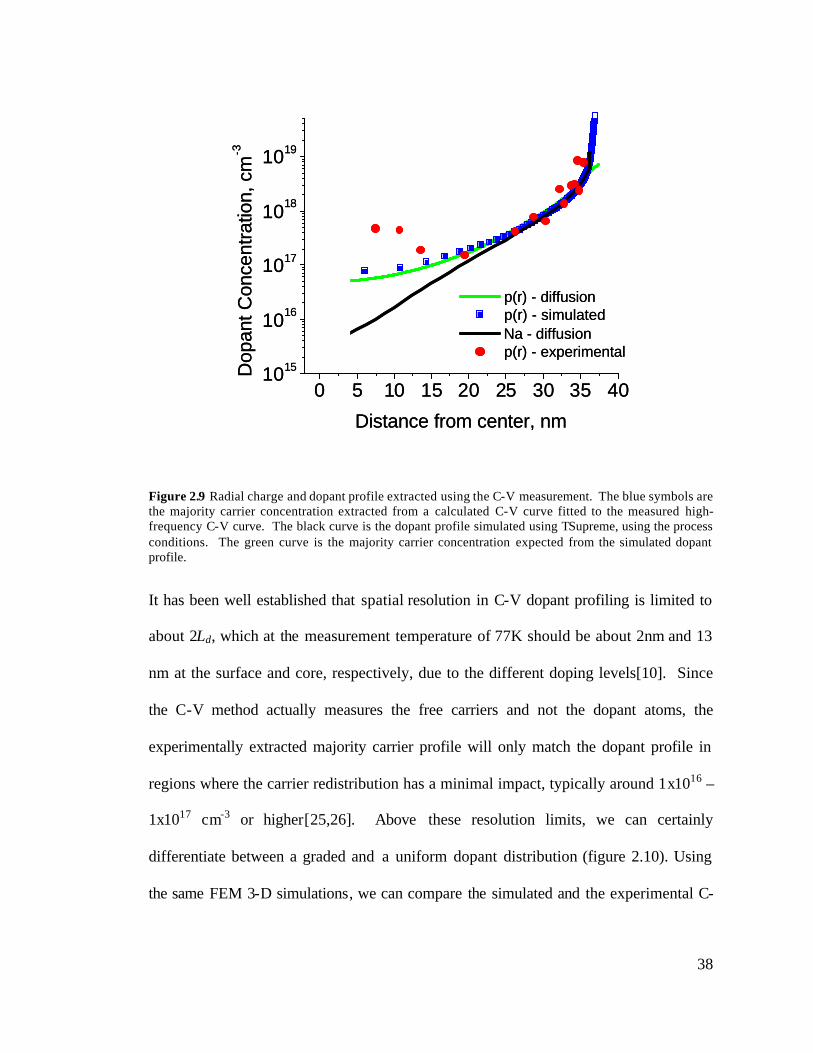
differentiate between a graded and a uniform dopant distribution (figure 2.10). Using
the same FEM 3-D simulations, we can compare the simulated and the experimental C-
39
V curves in order to determine the flat band voltage (VFB) and further validate our
dopant profiling and Dit extraction techniques.
-1 0 1
0.0
0.5
1.0
1.5
2.0
2.5
3.0C
, fF
Gate Voltage, V
Simulated C-V, Flat Profile, Shifted Simulated C-V, Diffusion Profile Experimental C-V
Figure 2.10 Simulated C-V curves. Experimental high frequency 20 kHz C-V curve (blue) compared to the simulated C-V curves for the boron diffusion profile (black) and the flat profile (red) as shown in Figure 4a and 4b, respectively. Credit: D. Khanal.
Figure 2.10 shows the FEM simulated C-V curves calculated from the graded and the
uniform profiles (Na=1017/cm3), and the high-frequency (20 kHz) experimental C-V
curve. The simulated curves are shifted horizontally so they overlap one another, for
the purpose of comparison. Without this shift, VFB for the uniform profile would be
about 0V. Clearly, the graded dopant profile leads to a C-V curve that matches the
experimental C-V curve better than a uniform dopant profile.
40
The only major deviation comes at full depletion where the simulated
capacitance reduces to 0fF, while the experimental curve does not go below 0.5fF. This
extra capacitance in the experiment may come from direct coupling between the
surround gate and the nanowire leads. The simulation does not account for this since it
does not incorporate a back gate and thus allows for the leads (underlapped regions) to
become depleted. Since the simulation did not account for interfacial defects, the minor
deviation in slope likely stems from interface states, which are known to cause stretch-
out even in high frequency C-V measurements[10].
In figure 2.10, it is necessary to shift the simulated C-V curve horizontally to
match the measurement. Attributing this flat-band voltage shift to the built- in potential
between the metal gate and the substrate and the contribution from fixed charges, we
can extract a fixed oxide charge density of Qi=-4.6 x1011 cm-2, when a literature value
for chromium (f M=4.5eV) is used. This value of Qi is similar to previous literature
reports for Al2O3 deposited using ALD[16].
Lastly, it should be noted that although this experiment was conduc ted at 77K,
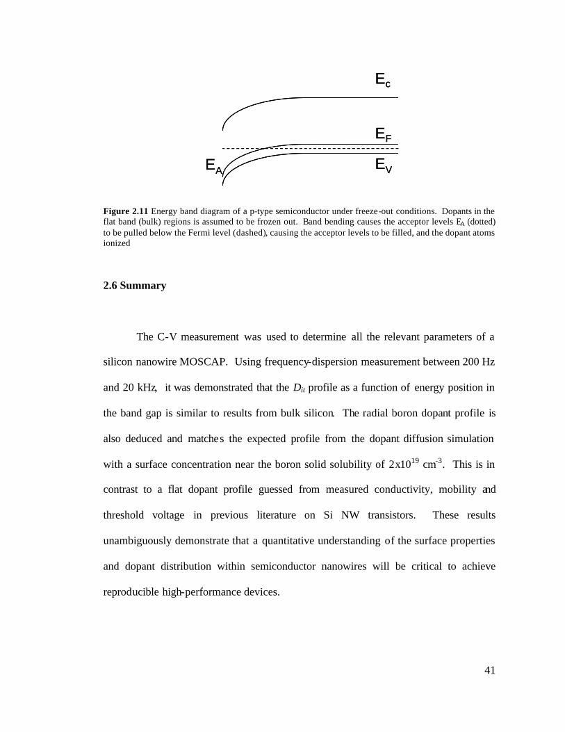
dopant freeze-out need not to be considered. As illustrated in figure 2.11, dopants are
still ionized in the depleted region because the impurity acceptor level EA is pulled
below the Fermi level, causing it to be filled, and the acceptor impurities to be fully
ionized (figure 2.11). Thus, this technique can in principle be extended for even lower
dopant densities, if the temperature is lowered further.
41
EF
Ec
EVEA
EF
Ec
EVEA
Figure 2.11 Energy band diagram of a p-type semiconductor under freeze-out conditions. Dopants in the flat band (bulk) regions is assumed to be frozen out. Band bending causes the acceptor levels EA (dotted) to be pulled below the Fermi level (dashed), causing the acceptor levels to be filled, and the dopant atoms ionized
2.6 Summary
The C-V measurement was used to determine all the relevant parameters of a
silicon nanowire MOSCAP. Using frequency-dispersion measurement between 200 Hz
and 20 kHz, it was demonstrated that the Dit profile as a function of energy position in
the band gap is similar to results from bulk silicon. The radial boron dopant profile is
also deduced and matches the expected profile from the dopant diffusion simulation
with a surface concentration near the boron solid solubility of 2x1019 cm-3. This is in
contrast to a flat dopant profile guessed from measured conductivity, mobility and
threshold voltage in previous literature on Si NW transistors. These results
unambiguously demonstrate that a quantitative understanding of the surface properties
and dopant distribution within semiconductor nanowires will be critical to achieve
reproducible high-performance devices.
42
References
[1] Cui, Y., Wei, Q. Q., Park, H. K. and Lieber, C. M. Science 293, 1289-1292 (2001).
[2] Feng, X. L., He, R. R., Yang, P. D. and Roukes, M. L. Nano Letters 7, 1953-1959
(2007).
[3] Kayes, B. M., Atwater, H. A. and Lewis, N. S. J. Appl. Phys. 97, 114302 (2005).
[4] Garnett, E. C. and Yang, P. D. J. Am. Chem. Soc. 130, 9224-9225 (2008).
[5] Hochbaum, A. I. et al. Nature 451, 163-168 (2008).
[6] Law, M., Goldberger, J. and Yang, P. D. Annual Review of Materials Research 34,
83-122 (2004).
[7] Goldberger, J., Hochbaum, A. I., Fan, R. and Yang, P. D. Nano Letters 6, 973-977
(2006).
[8] Goldberger, J., Sirbuly, D. J., Law, M. and Yang, P. J Phys Chem B 109, 9-14
(2005).
[9] Cui, Y., Duan, X. F., Hu, J. T. and Lieber, C. M. J Phys Chem B 104, 5213-5216
(2000).
[10] Nicollian, E. H. and Brews, J. R. in MOS Physics and Technology 1-903 (Wiley-
Interscience, New York, 1982).
[11] Tu, R., Zhang, L., Nishi, Y. and Dai, H. J. Nano Letters 7, 1561-1565 (2007).
[12] Gunawan, O. et al. Nano Letters, 8, 1566–1571 (2008).
[13] S. Roddaro et al, Appl. Phys. Lett.,92, 253509 (2008) [14] Ilani, S., Donev, L. A. K., Kindermann, M. and McEuen, P. L. Nature Physics 2,
687-691 (2006).
[15] He, R. R. et al. Adv Mater 17, 2098-2102 (2005).
43
[16] He, R. and Yang, P. Nat. Nanotech. 1, 42-46 (2006).
[17] A. San Paulo, N. Arellano, J.A. Plaza et al, Nano Lett. 7, 1100-1104 (2007) [18] Wilk, G. D., Wallace, R. M. and Anthony, J. M. J. Appl. Phys. 89, 5243-5275
(2001).
[19] Truong, L., Fedorenko, Y. G., Afanasev, V. V. and Stesmans, A. Microelectronics
Reliability 45, 823-826 (2005).
[20] Duenas, S. et al. J. Appl. Phys. 99, 054902 (2006).
[21] Kim, T. W. et al. J. Appl. Phys. 74, 760-762 (1993).
[22] R.S. Wagner and W.C. Ellis, Appl. Phys. Lett. 4, 89-90 (1964). [23] Terman, L. M. Solid-State Electronics 5, 285-299 (1962).
[24] Sze, S. M. in Physics of Semiconductor Devices 1-812 (Wiley-Interscience, New
York, 1969).
[25] Kennedy, D. P., Murley, P. C. and Kleinfel.W. IBM Journal of Research and
Development 12, 399-409 (1968).
[26] Kennedy, D. P. and Obrien, R. R. Ibm Journal of Research and Development 13,
212-213 (1969).
44
Chapter 3
Characterization of back-gated InAs nanowires
Transistors have been reducing in size ever since their introduction into
integrated circuits. The international technology roadmap predicts that by the
completion of this thesis, the gate length of a MOS transistor will be about 32nm. One
of the reasons for transistor scaling is to improve switching performance. Even in the
velocity-saturation regime, reducing the channel length of the transistor can still
improve the drive current[1], as long as the transport is not completely ballistic.
It is well known that carrier mobility is much higher in III-V semiconductors
compared to silicon. However, their usage as a channel material in a MOSFET
structure is limited by the unavailability of a gate dielectric with sufficiently good
45
interface quality. Transistors based on bottom-up semiconductor materials such as
nanowires of Si[2], Ge[3], InAs[4] or carbon nanotubes[5] are shown to have a carrier
mobility generally much greater than transistors made in bulk silicon. However, most
prior estimates of the mobility were based on rather simple calculation of the gate
capacitance[1,2]. In these primitive devices, the channel is often back-gated because
that geometry is easy to realize, and one can dispense with gate dielectric s that usually
have a deleterious impact on the mobility, although a passivated surface is still
necessary. As a result, the dielectric medium surround ing the channel (figure 3.1) is not
uniform and the gate capacitance is somewhat difficult to model. A simple alternative
is to measure the capacitance directly, and use this information to extract accurate
mobility numbers.
In this chapter the C-V technique is used to characterize individual InAs
nanowire in its usual back-gated geometry, both to extract the oxide capacitance
accurately, and to characterize the interface quality, in terms of usual parameters such as
interface trap density and trap life time.
46
SiO2
Back Gate
NWe= 1
e= 3.9
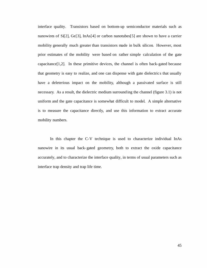
Figure 3. 1 Cross-section of a commonly used geometry for nanowire devices. The back gate is used to modulate the conductivity of the nanowire channel.
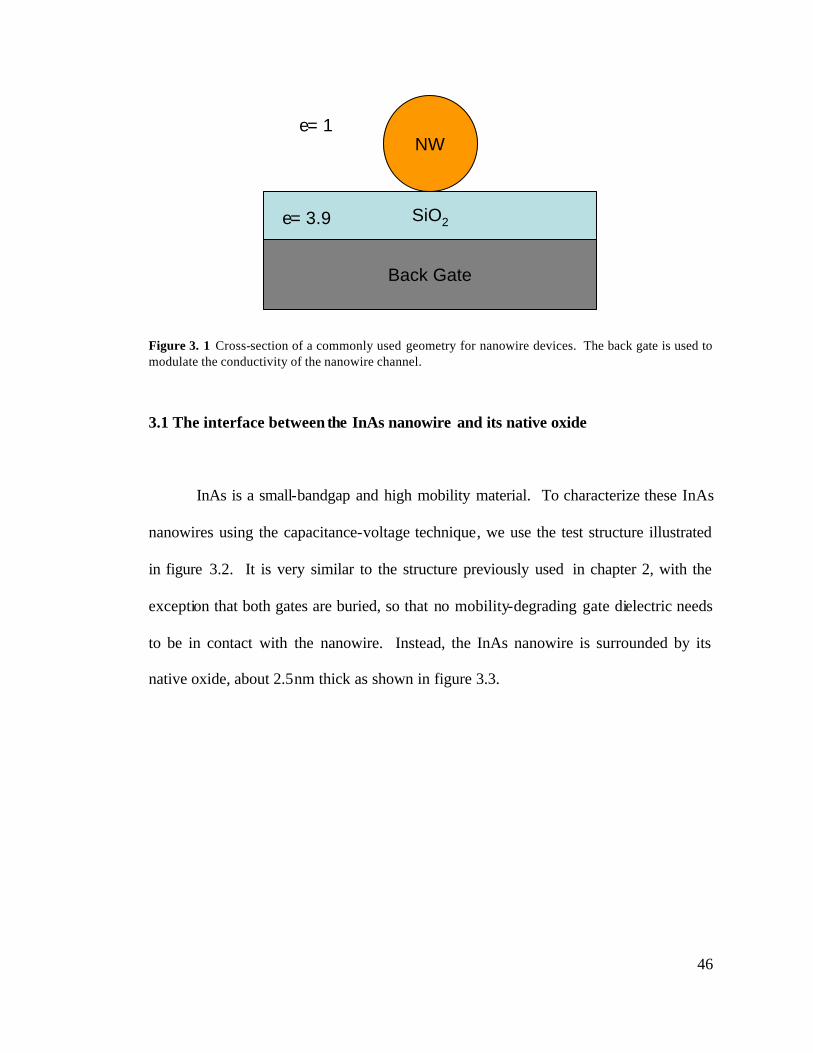
3.1 The interface between the InAs nanowire and its native oxide
InAs is a small-bandgap and high mobility material. To characterize these InAs
nanowires using the capacitance-voltage technique, we use the test structure illustrated
in figure 3.2. It is very similar to the structure previously used in chapter 2, with the
exception that both gates are buried, so that no mobility-degrading gate dielectric needs
to be in contact with the nanowire. Instead, the InAs nanowire is surrounded by its
native oxide, about 2.5nm thick as shown in figure 3.3.
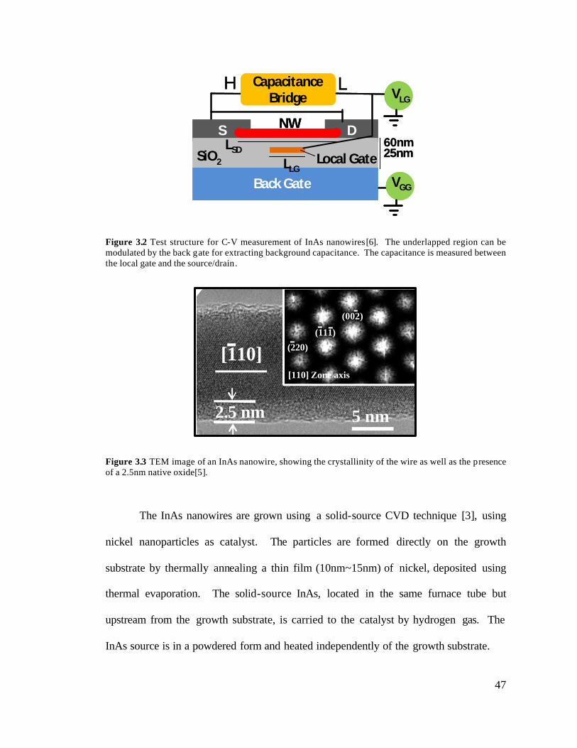
47
S D
Local Gate
Back Gate
NW
SiO2 LLG
LSD60nm
Capacitance Bridge VLG
25nm
VGG
H L
S D
Local Gate
Back Gate
NW
SiO2 LLG
LSD60nm
Capacitance Bridge VLG
25nm
VGG
H L
Figure 3.2 Test structure for C-V measurement of InAs nanowires[6]. The underlapped region can be modulated by the back gate for extracting background capacitance. The capacitance is measured between the local gate and the source/drain.
5 nm2.5 nm
(002)
(220)
(111)
[110] Zone axis
[110]
Figure 3.3 TEM image of an InAs nanowire, showing the crystallinity of the wire as well as the presence of a 2.5nm native oxide[5].
The InAs nanowires are grown using a solid-source CVD technique [3], using
nickel nanoparticles as catalyst. The particles are formed directly on the growth
substrate by thermally annealing a thin film (10nm~15nm) of nickel, deposited using
thermal evaporation. The solid-source InAs, located in the same furnace tube but
upstream from the growth substrate, is carried to the catalyst by hydrogen gas. The
InAs source is in a powdered form and heated independently of the growth substrate.

48
The test structure is fabricated following the process sequence illustrated in
figure 3.4. Starting with a heavily doped p-type silicon wafer, a thick layer (200nm) of
thermal oxide is grown (3.4a). The buried local gate is fabricated by partially etching
away the thick oxide layer using buffered HF, in the area defined lithographically in a
photoresist bilayer (3.4b). The drawn length of the gate varies from 2µm to 8µm.
Metal (Pt) is then deposited and lifted off using the same photoresist bilayer. A thin
(50nm) layer of CVD oxide is then deposited to insulate the buried local gate from the
nanowire.
a
b
c
d
e
f
a
b
c
d
e
f
Figure 3.4 Fabrication process sequence of the C-V test structure. a) Growth of thermal oxide (yellow). b) Definition of the buried electrode, by etching into the oxide using buffered HF. Pt (green) deposition and lift-off follows, resulting in (c). Lift-off is facilitated by the bilayer resist. d) Deposition of a 50nm silicon dioxide. e) Deposition of InAs nanowires from ethanol suspension onto the entire substrate. f) Definition of the nickel source and drain electrodes. Process designed by J.C.Ho.

49
The InAs nanowires are then desposited from a suspension in ethanol. The nanowire
density is large enough such that about 5 to10 devices with only a single nanowire can
be found on each 1”x1” chip. Lastly, nickel source and drain electrodes are defined
using a second lift-off step. A brief (~30s) rapid thermal anneal follows to improve the
contact resistance.
The method for accurate C-V measurement and background extraction follows
the description in chapter 2. Figure 3.5 shows a typical C-V curve measured at 77K. At
this temperature, the lifetime of the surface states is too long to respond to the applied
signal frequency (1-20kHz). At a higher temperature, there is significant frequency
dispersion in the C-V curves, as seen in figure 3.6. Above 200K, the lifetime of the
traps is short enough to respond to even the highest frequency (20kHz) of the
instrument. The capacitance from the traps completely dominates, such that the wire
cannot be depleted and an accurate measurement of the background can not be done.
Indeed, a recent report[7] shows that frequency as high as 20MHz is necessary at room
temperature to stop the traps from responding.

50
250
200
150
100
50
0 C
apac
itanc
e (a
F)
-4 -2 0 2 4VGS (V)
2 kHz 20 kHz
77 K
Figure 3.5 Typical C-V curves at 77K for an InAs nanowire. There is a lack of frequency dispersion at such a low temperature.
A single time constant model for the trap lifetime successfully reproduces the
frequency-dispersion effect in figure 3.6. Based on this model, a surface trap density Dit
of ~1011 to 1012/ eV cm2 can be extracted from the C-V curves (figure 3.7). The capture
cross-section s p of the trap can also be estimated by using equation 3.1 [8]:
nv pσ
τ1
= (3.1)
where t, v and n are respectively the trap lifetime, thermal velocity and carrier density.
n can be calculated using a commercial three-dimensional device simulator, Taurus 3D,
and is remarkably uniform throughout the wire, despite the back-gate geometry (figure
3.8).
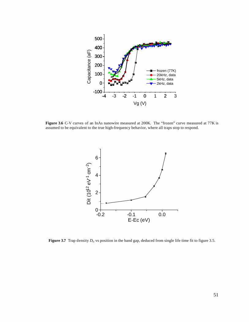
51
-4 -3 -2 -1 0 1 2 3-100
0
100
200
300
400
500
Cap
acita
nce
(aF)
Vg (V)
frozen (77K) 20kHz, data 5kHz, data 2kHz, data
-4 -2 0 2-100
0
100
200
300
400
500
Figure 3.6 C-V curves of an InAs nanowire measured at 200K. The “frozen” curve measured at 77K is assumed to be equivalent to the true high-frequency behavior, where all traps stop to respond.
-0.2 -0.1 0.00
2
4
6
Dit
(1012
eV
-1 c
m-2
)
E-Ec (eV)
Figure 3.7 Trap density Dit vs position in the band gap, deduced from single life time fit to figure 3.5.
52
0 5 10 15 20
1.0
1.1
1.2
1.3
1.4
1.5
Nor
mal
ized
Car
rier
Con
cent
ratio
n
Distance from gate oxide (nm)
Surface potential:
0.12V
0.032V
-0.067V
-0.143V
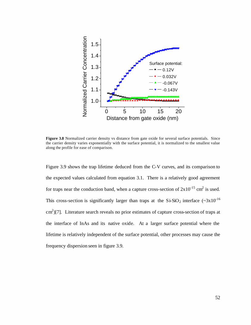
Figure 3.8 Normalized carrier density vs distance from gate oxide for several surface potentials. Since the carrier density varies exponentially with the surface potential, it is normalized to the smallest value along the profile for ease of comparison.
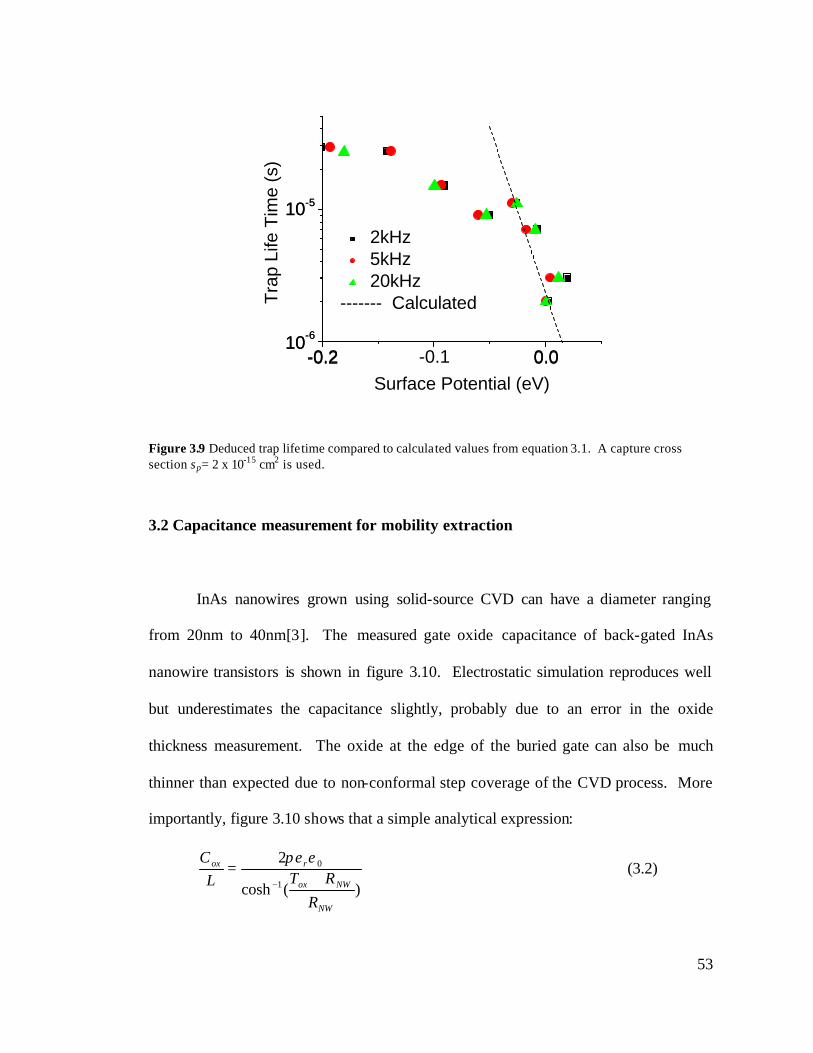
Figure 3.9 shows the trap lifetime deduced from the C-V curves, and its comparison to
the expected values calculated from equation 3.1. There is a relatively good agreement
for traps near the conduction band, when a capture cross-section of 2x10-15 cm2 is used.
This cross-section is significantly larger than traps at the Si-SiO2 interface (~3x10-16
cm2)[7]. Literature search reveals no prior estimates of capture cross-section of traps at
the interface of InAs and its native oxide. At a larger surface potential where the
lifetime is relatively independent of the surface potential, other processes may cause the
frequency dispersion seen in figure 3.9.
53
-0.2 0.010-6
10-5
-0.2 -0.1 0.010-6
10-5
Tra
p Li
fe T
ime
(s)
Surface Potential (eV)
2kHz 5kHz 20kHz
------- Calculated
Figure 3.9 Deduced trap lifetime compared to calculated values from equation 3.1. A capture cross section sp= 2 x 10-15 cm2 is used.
3.2 Capacitance measurement for mobility extraction
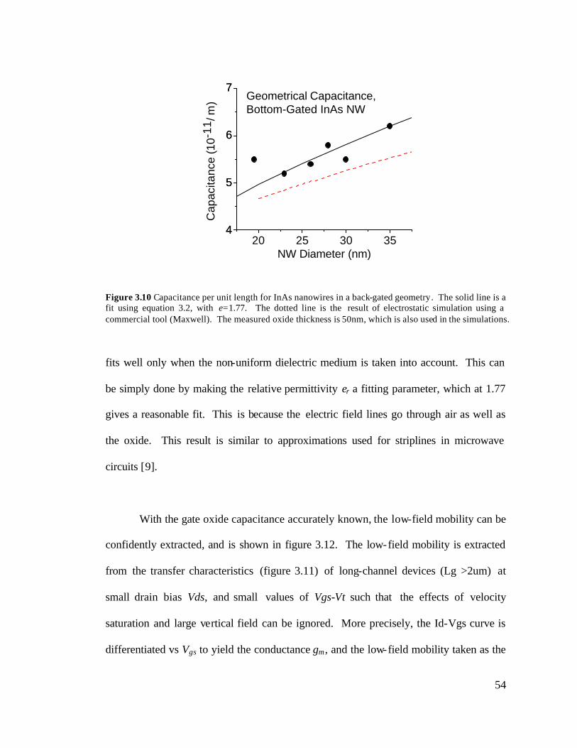
InAs nanowires grown using solid-source CVD can have a diameter ranging
from 20nm to 40nm[3]. The measured gate oxide capacitance of back-gated InAs
nanowire transistors is shown in figure 3.10. Electrostatic simulation reproduces well
but underestimates the capacitance slightly, probably due to an error in the oxide
thickness measurement. The oxide at the edge of the buried gate can also be much
thinner than expected due to non-conformal step coverage of the CVD process. More
importantly, figure 3.10 shows that a simple analytical expression:
)(cosh
2
1
0
NW
NWox
rox
RRTL
C+
=−
επε (3.2)
54
20 25 30 354
5
6
7
4
5
6
7
Cap
acita
nce
(10-
11/ m
)
NW Diameter (nm)
Geometrical Capacitance, Bottom-Gated InAs NW
Figure 3.10 Capacitance per unit length for InAs nanowires in a back-gated geometry. The solid line is a fit using equation 3.2, with e=1.77. The dotted line is the result of electrostatic simulation using a commercial tool (Maxwell). The measured oxide thickness is 50nm, which is also used in the simulations.
fits well only when the non-uniform dielectric medium is taken into account. This can
be simply done by making the relative permittivity er a fitting parameter, which at 1.77
gives a reasonable fit. This is because the electric field lines go through air as well as
the oxide. This result is similar to approximations used for striplines in microwave
circuits [9].
With the gate oxide capacitance accurately known, the low-field mobility can be
confidently extracted, and is shown in figure 3.12. The low-field mobility is extracted
from the transfer characteristics (figure 3.11) of long-channel devices (Lg >2um) at
small drain bias Vds, and small values of Vgs-Vt such that the effects of velocity
saturation and large vertical field can be ignored. More precisely, the Id-Vgs curve is
differentiated vs Vgs to yield the conductance gm, and the low-field mobility taken as the
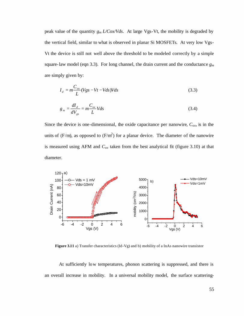
55
peak value of the quantity gm L/Cox/Vds. At large Vgs-Vt, the mobility is degraded by
the vertical field, similar to what is observed in planar Si MOSFETs. At very low Vgs-
Vt the device is still not well above the threshold to be modeled correctly by a simple
square- law model (eqn 3.3). For long channel, the drain current and the conductance gm
are simply given by:
VdsVdsVtVgsL
CI ox
d )( −−= µ (3.3)
VdsL
CdVdI
g ox
gs
dm µ== (3.4)
Since the device is one-dimensional, the oxide capacitance per nanowire, Cox, is in the
units of (F/m), as opposed to (F/m2) for a planar device. The diameter of the nanowire
is measured using AFM and Cox taken from the best analytical fit (figure 3.10) at that
diameter.
-6 -4 -2 0 2 4 6
0
20
40
60
80
100
120 a)
Dra
in C
urre
nt (
nA)
Vgs (V)
Vds = 1 mV Vds=10mV
-6 -4 -2 0 2 4 6
0
1000
2000
3000
4000
5000 b)
mob
ility
(cm
2 /V
s)
Vgs (V)
Vds=10mV Vds=1mV
Figure 3.11 a) Transfer characteristics (Id-Vg) and b) mobility of a InAs nanowire transistor
At sufficiently low temperatures, phonon scattering is suppressed, and there is
an overall increase in mobility. In a universal mobility model, the surface scattering-
56
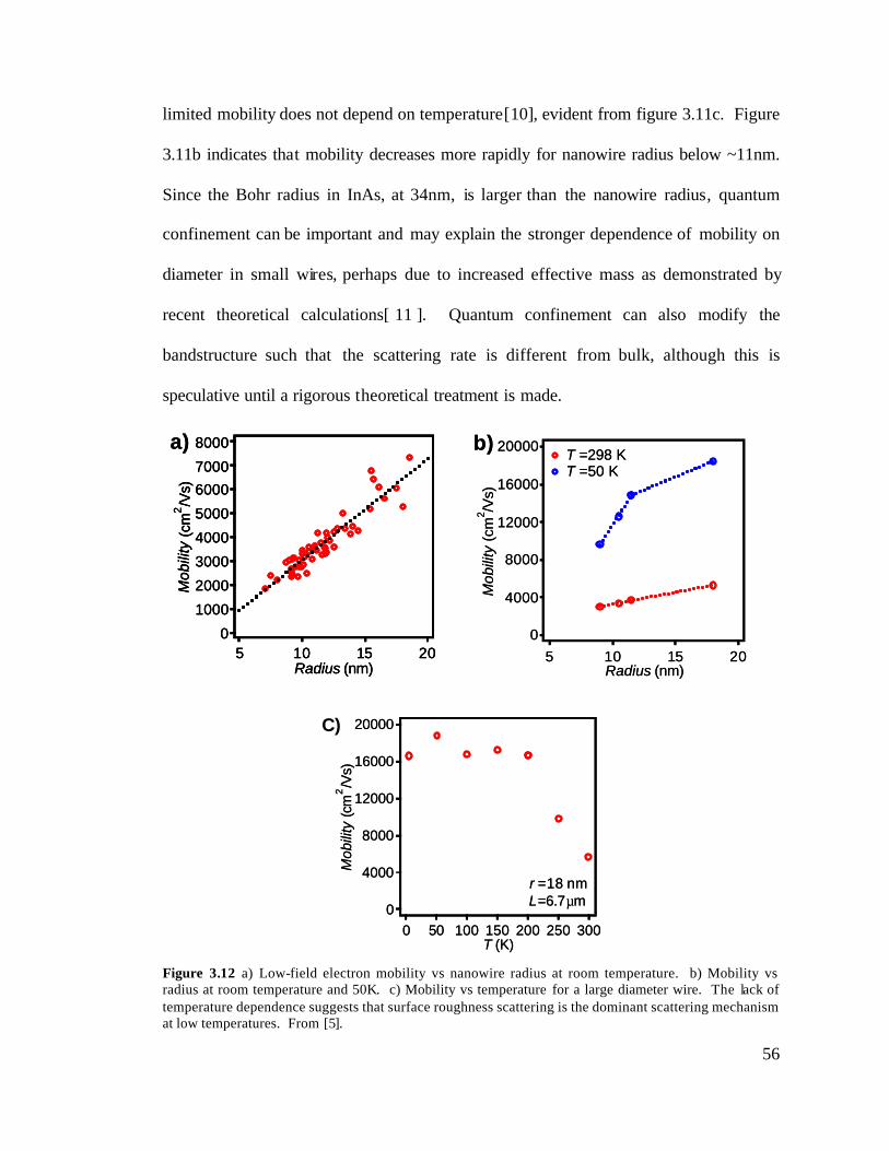
limited mobility does not depend on temperature[10], evident from figure 3.11c. Figure
3.11b indicates that mobility decreases more rapidly for nanowire radius below ~11nm.
Since the Bohr radius in InAs, at 34nm, is larger than the nanowire radius, quantum
confinement can be important and may explain the stronger dependence of mobility on
diameter in small wires, perhaps due to increased effective mass as demonstrated by
recent theoretical calculations[ 11 ]. Quantum confinement can also modify the
bandstructure such that the scattering rate is different from bulk, although this is
speculative until a rigorous theoretical treatment is made.
a) 8000
7000
6000
5000
4000
3000
2000
1000
0
Mob
ility
(cm
2/V
s)
2015105Radius (nm)
a) 8000
7000
6000
5000
4000
3000
2000
1000
0
Mob
ility
(cm
2/V
s)
2015105Radius (nm)
8000
7000
6000
5000
4000
3000
2000
1000
0
Mob
ility
(cm
2/V
s)
2015105Radius (nm)
b) 20000
16000
12000
8000
4000
0
Mob
ility
(cm
2 /Vs)
2015105Radius (nm)
T =298 K
T =50 K
b) 20000
16000
12000
8000
4000
0
Mob
ility
(cm
2 /Vs)
2015105Radius (nm)
T =298 K
T =50 K
20000
16000
12000
8000
4000
0
Mob
ility
(cm
2/V
s)
300250200150100500T (K)
r =18 nm L=6.7µm
C) 20000
16000
12000
8000
4000
0
Mob
ility
(cm
2/V
s)
300250200150100500T (K)
r =18 nm L=6.7µm
C)
Figure 3.12 a) Low-field electron mobility vs nanowire radius at room temperature. b) Mobility vs radius at room temperature and 50K. c) Mobility vs temperature for a large diameter wire. The lack of temperature dependence suggests that surface roughness scattering is the dominant scattering mechanism at low temperatures. From [5].
57
3.3 Summary and Future Work
In this chapter, low-level C-V measurement and analysis are used to deduce the
relevant parameters that describe the surface states of a single InAs nanowire. In
addition, it is shown that a simple analytical expression predicts well the geometrical
gate oxide capacitance, provided that the non-homogeneous dielectric medium is
accounted for. The accurate measurement of the oxide capacitance allows for an
accurate determination of the carrier mobility in InAs nanowires. When phonon
scattering is suppressed at low temperatures, the dominant mechanism for small-
diameter nanowires seems to be surface scattering.
There are other properties of InAs nanowires that can be probed using this
technique, one of which is the quantization effect arising from the small diameter. Ilani
et al used the same technique to probe the density of states in a single carbon
nanotube[12]. Figure 3.12 shows much more precise C-V measurements of two small
InAs nanowires at liquid helium temperature, and the comparison to simulation. There
are small but interesting features that cannot be reproduced by a straightforward
electrostatic simulation employing bulk density of states.

58
-2 0 2 4 60.0
0.2
0.4
0.6
0.8
1.0
Nor
mal
ized
Cap
acita
nce
(C/C
ox)
Gate Voltage (V)
19nm 26nm Simulation, 4.2K
Figure 3.13 Measured C-V curves of two small diameter InAs nanowires at 4K. The measurement frequency is 100kHz. Simulation: diameter=20nm
At the temperature of liquid helium, the traps should have ceased to respond, as implied
from the results at liquid nitrogen temperature (figure 3.5). Since the nanowire is
undoped, the observed features in the C-V curves cannot be caused by ionized dopants
either. The most plausible explanation is that there is a transition of the density of state
in the nanowire from bulk- like to that of a one-dimensional quantum wire. At this
moment, there is no known method to make much thinner InAs nanowires without
increasing significantly the surface roughness. Should a solution be found, the one-
dimensional band structure of an individual InAs nanowire can be directly probed using
this method.
59
References
[1] A. Khakifirooz and D.A.Antoniadis, IEEE Tran.s on Elec. Dev. 55, 1391-1400 (2008) [2] Y. Cui, Z. Zhong, D. Wang, W.U. Wang, C.M. Lieber, Nano Lett. 3, 149-152 (2003)
[ 3 ] D. Wang, Q. Wang, A. Javey, R. Tu, H. Dai, H. Kim, P.C. McIntyre, T.
Krishnamohan, K.C. Saraswat, Appl. Phys. Lett., 83, 2432-2434 (2003)
[4] A.C. Ford, J.C. Ho, Z. Fan, O. Ergen, V. Altoe, S. Aloni, H. Razavi, A. Javey, Nano
Research, 1, 32-39 (2008)
[5] A. Javey, J Guo, Q. Wang, M. Lundstrom, H. Dai, Nature, 424, 654-657 (2003)
[6] A. Ford, J. Ho, Y.L. Chueh, Y.C. Tseng, Z. Fan, J. Guo, J. Bokor and A. Javey,
Nano Letters, 9, 360-365 (2009)
[7 ] S. Roddaro, K. Nilsson, G. Astromskas, L. Samuelsson, L.E. Wernersson, O.
Karlstrom, A. Wacker, Appl. Phys. Lett., 92, 253509 (2008).
[8] S. Sze, Physics of Semiconductor Devices, 2nd edition.
[9] D.M. Pozar, Microwave Engineering 2nd edition, Wiley, 1998
[10] S. Takagi, A. Toriumi, M. Iwase, H. Tango, IEEE Trans. Elec. Dev., 41, 2363-
2368 (1994).
[11] B. Lassen, M. Willatzen, R. Melnik, L.C. Lew Yan Voon, J. Mater. Res., 21, 2927-
2935 (2006).
[12] S. Ilani, L. Donev, F. Kindermann, P. McEuen, Nature Physics, 2, 687-691 (2006).
60
Chapter 4
Metal-Carbon Nanotube Schottky Contacts
The metal-semiconductor (MS) contact is ubiquitous in semiconductor devices.
By itself, a Schottky MS contact, with low substrate doping and large barrier height, can
be used as a high-speed rectifier. In other devices such as MOSFETs and BJTs, the MS
contact is absolutely necessary for their integration into circuits. These contacts need to
have a low specific resistance in order for the devices to function properly. This is
usually achieved by doping the contact region heavily to allow tunneling through a
thinned Schottky barrier. In the current Si-based MOS technology, the MS contact is a
major contributor to serial, parasitic resistances that degrade transistor performance. As

61
the dimensions of MOS transistors diminish further, the resistance of the MS contact
can become much more detrimental, since the source/drain junction will need to
become even more shallow and abrupt to combat short-channel effects, and the dopant
concentration in the source and drain can not go higher, being already limited by the
dopants’ solid solubility.
Similarly, in transistors made from high-mobility materials such as carbon
nanotubes, the Schottky barrier (SB) at the source and drain contacts can severely
degrade the device performance, to the point that they completely determine the
behavior of the device[1,2,3]. CNT transistors with negligible Schottky barrier height
(SBH) and with minimal series resistance can be realized[4], and have a performance
that surpasses their silicon-based counterpart. However, there is a limited choice of
metal that can achieve this, such as Pd[4] and Rh[7], and a nanotube with large diameter
is invariably needed[4,5,7].
The SBH between a CNT and its metal contact depends on seve ral material
parameters, such as the metal contact work function[5], the environment to which the
device is exposed[6], and the diameter of the nanotube[7]. Given the many possible
sources of variation, it is desirable to study a large set of devices to obtain statistically
meaningful results on how each parameter impacts upon the device characteristics. The
electrical characteristics of several hundreds of CNT transistors are examined in this
chapter. Analysis of this data shows the influence of the nanotube diameter and the
contact metal on the operating characteristics of a CNT transistor. By examining the
62
variation of on- and off-state currents vs the diameter, conclusions can also be drawn,
surprisingly, about the geometry of the MS junction for a nanotube.
4.1 Prior work
There is a rich literature on Fermi- level pinning in bulk semiconductors, after
research in excess of 60 years[8,9,10]. Schottky proposed in 1938 that a potential
barrier occurs naturally at a metal-semiconductor junction due to workfunction
mismatch between the two materials. Contrary to the ideal Schottky model,
experimental evidence shows that the SBH does not vary much with the metal
workfunction[ 11 ]. This is because of the presence of electronic states inside the
bandgap that effectively pins the Fermi- level at a fixed position. In a typical bulk
semiconductor, the density of these states are sufficiently large that only a small fraction
needs to be populated to compensate for the charge induced by the metal-semiconductor
contact potential.
For contacts to one-dimensional semiconductors, an early theoretical study[12]
predicted that Fermi- level pinning is of negligible consequence to the contact resistance,
and that the junction is effectively unpinned. A few studies indicated that these
theoretical predictions seem to hold true. Both Chen[5] and Kim[7] showed that the on-
state current of a CNT transistor depends on the CNT diameter, and attributed the
variation in the on-state current to a diameter-dependent Schottky barrier height at the
contact. However, Chen et al[5] did not actually measure the diameter of each
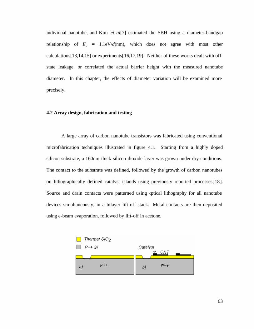
63
individual nanotube, and Kim et al[7] estimated the SBH using a diameter-bandgap
relationship of Eg = 1.1eV/d(nm), which does not agree with most other
calculations[13,14,15] or experiments[16,17,19]. Neither of these works dealt with off-
state leakage, or correlated the actual barrier height with the measured nanotube
diameter. In this chapter, the effects of diameter variation will be examined more
precisely.
4.2 Array design, fabrication and testing
A large array of carbon nanotube transistors was fabricated using conventional
microfabrication techniques illustrated in figure 4.1. Starting from a highly doped
silicon substrate, a 160nm-thick silicon dioxide layer was grown under dry conditions.
The contact to the substrate was defined, followed by the growth of carbon nanotubes
on lithographically defined catalyst islands using previously reported processes[18].
Source and drain contacts were patterned using optical lithography for all nanotube
devices simultaneously, in a bilayer lift-off stack. Metal contacts are then deposited
using e-beam evaporation, followed by lift-off in acetone.

64
Figure 4.1 Process steps for making a large number of CNT devices for automated measurement. a) Contact to substrate. b) Growth of nanotubes. c) Bilayer of lift-off stack, photoresist on top of PMMA, the latter of which is selectively dissolved in chlorobenzene. d) Deposition and lift -off of metal contacts.
Figure 4.2 Scanning electron micrograph of an actual device. 896 such devices are packed into an 1cm2
chip.
The gate length, set by the gap between source and drain, is 2 µm. Figure 4.2 shows the
top view of a device. Since the CNTs do not align in any particular direction during
growth, the source and drain electrodes are designed to increase the probability of a
CNT bridging the contacts.
65
Since measuring a large number of devices manually would be intractable,
automated measurement is necessary. Shown in figure 4.3 is the array designed for
measurement using the Electroglas 2001X automatic prober. 896 devices are packed
into a single cm2 chip, and the entire measurement requires approximately 3 hours.
Since there is no control over the chirality and the number of nanotubes in each device,
we can only sort the devices after the measurement, based on the I-V data. From the
transfer characteristics of each device, those with metallic tubes (low on/off ratio) are
found, and eliminated from consideration. Devices that remain are inspected
individually using SEM, and only those with a single tube bridging the contacts are to
be analyzed. The diameter of the nanotube is measured using tapping mode atomic
force microscopy (AFM, Digital Instruments 3100), and is taken as the height of the
nanotube relative to the substrate, averaged over a length of several hundred
nanometers. The one-sigma uncertainty in each measurement is estimated to be 0.2nm
and corresponds well to the RMS roughness of the oxide substrate itself, indicating that
the precision of the measurement is probably limited by the substrate roughness.
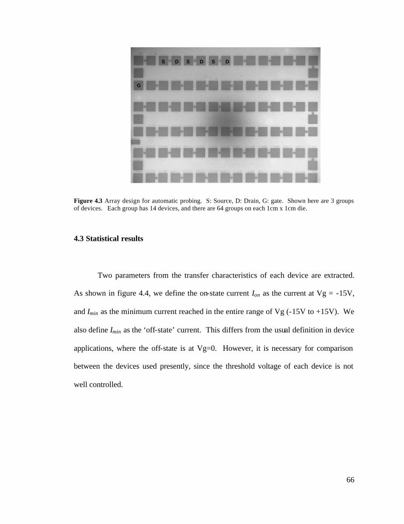
66
S S SD D D
G
Figure 4.3 Array design for automatic probing. S: Source, D: Drain, G: gate. Shown here are 3 groups of devices. Each group has 14 devices, and there are 64 groups on each 1cm x 1cm die.
4.3 Statistical results
Two parameters from the transfer characteristics of each device are extracted.
As shown in figure 4.4, we define the on-state current Ion as the current at Vg = -15V,
and Imin as the minimum current reached in the entire range of Vg (-15V to +15V). We
also define Imin as the ‘off-state’ current. This differs from the usual definition in device
applications, where the off-state is at Vg=0. However, it is necessary for comparison
between the devices used presently, since the threshold voltage of each device is not
well controlled.
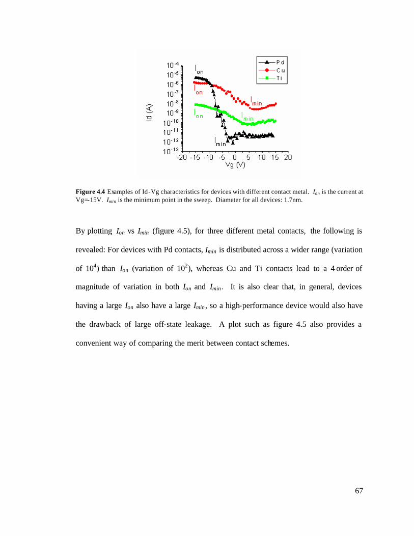
67
Figure 4.4 Examples of Id-Vg characteristics for devices with different contact metal. Ion is the current at Vg=-15V. Imin is the minimum point in the sweep. Diameter for all devices: 1.7nm.
By plotting Ion vs Imin (figure 4.5), for three different metal contacts, the following is
revealed: For devices with Pd contacts, Imin is distributed across a wider range (variation
of 104) than Ion (variation of 102), whereas Cu and Ti contacts lead to a 4-order of
magnitude of variation in both Ion and Imin. It is also clear that, in general, devices
having a large Ion also have a large Imin, so a high-performance device would also have
the drawback of large off-state leakage. A plot such as figure 4.5 also provides a
convenient way of comparing the merit between contact schemes.
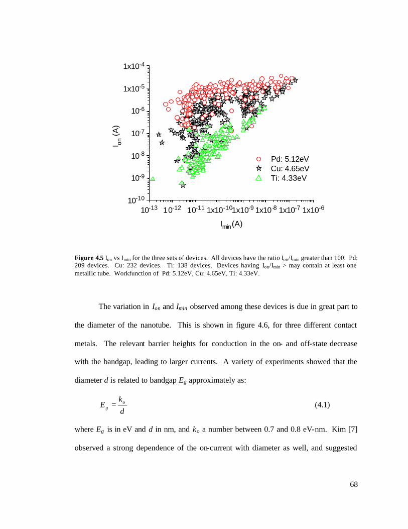
68
10-13 10-12 10-11 1x10-101x10-9 1x10 -8 1x10⁻⁷ 1x10-610-10
10-9
10-8
10-7
10-6
1x10⁻⁵
1x10⁻⁴
I on (
A)
Imin(A)
Pd: 5.12eV Cu: 4.65eV Ti: 4.33eV
Figure 4.5 Ion vs Imin for the three sets of devices. All devices have the ratio Ion/Imin greater than 100. Pd: 209 devices. Cu: 232 devices. Ti: 138 devices. Devices having Ion/Imin > may contain at least one metallic tube. Workfunction of Pd: 5.12eV, Cu: 4.65eV, Ti: 4.33eV.
The variation in Ion and Imin observed among these devices is due in great part to
the diameter of the nanotube. This is shown in figure 4.6, for three different contact
metals. The relevant barrier heights for conduction in the on- and off-state decrease
with the bandgap, leading to larger currents. A variety of experiments showed that the
diameter d is related to bandgap Eg approximately as:
dk
E og = (4.1)
where Eg is in eV and d in nm, and ko a number between 0.7 and 0.8 eV-nm. Kim [7]
observed a strong dependence of the on-current with diameter as well, and suggested
69
that ko is 1.1 eV-nm, significantly larger than other experiments. Tight-binding
calculations [28] predict that:
d
aE occ
g
γ2=
where acc=0.144nm and ?o are respectively the distance and the interaction energy
between the two nearest carbon atoms. DFT calculations [15] give ?o =2.6eV, while a
resonant Raman scattering experiment [17] employs ?o=2.9eV to unambiguously predict
the resonant energy, and the associated chiralities of many nanotubes. Independent
results by Wildoer and Odom [16] from scanning tunneling spectroscopy show that
Eg˜ 0.7/d, which gives ?o=2.5eV. Bosnick et al [19] deduced from the I-V measurement
of a few p- i-n CNT diodes that Eg˜0.8/d, leading to ?o=2.85eV. These experimental
results differ considerably from the suggestion by Kim [7] that Eg=1.1/d, (?o =3.8eV)
which in his case only served to conveniently explain a rapid drop-off in the on-current
for diameters below 1.5nm. It will be shown in section 5.4 that the precise relationship
between SBH and diameter (bandgap) has implications on the actual geometry of the
electrical junction.
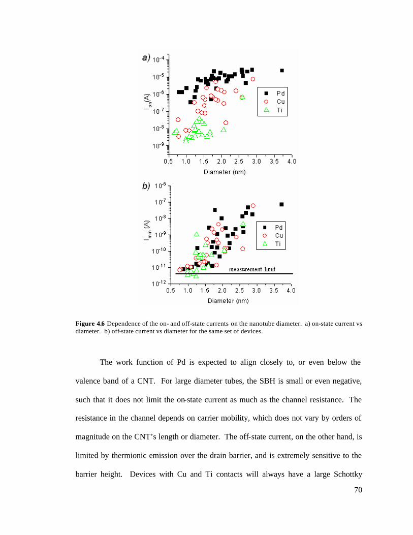
70
Figure 4.6 Dependence of the on- and off-state currents on the nanotube diameter. a) on-state current vs diameter. b) off-state current vs diameter for the same set of devices.
The work function of Pd is expected to align closely to, or even below the
valence band of a CNT. For large diameter tubes, the SBH is small or even negative,
such that it does not limit the on-state current as much as the channel resistance. The
resistance in the channel depends on carrier mobility, which does not vary by orders of
magnitude on the CNT’s length or diameter. The off-state current, on the other hand, is
limited by thermionic emission over the drain barrier, and is extremely sensitive to the
barrier height. Devices with Cu and Ti contacts will always have a large Schottky
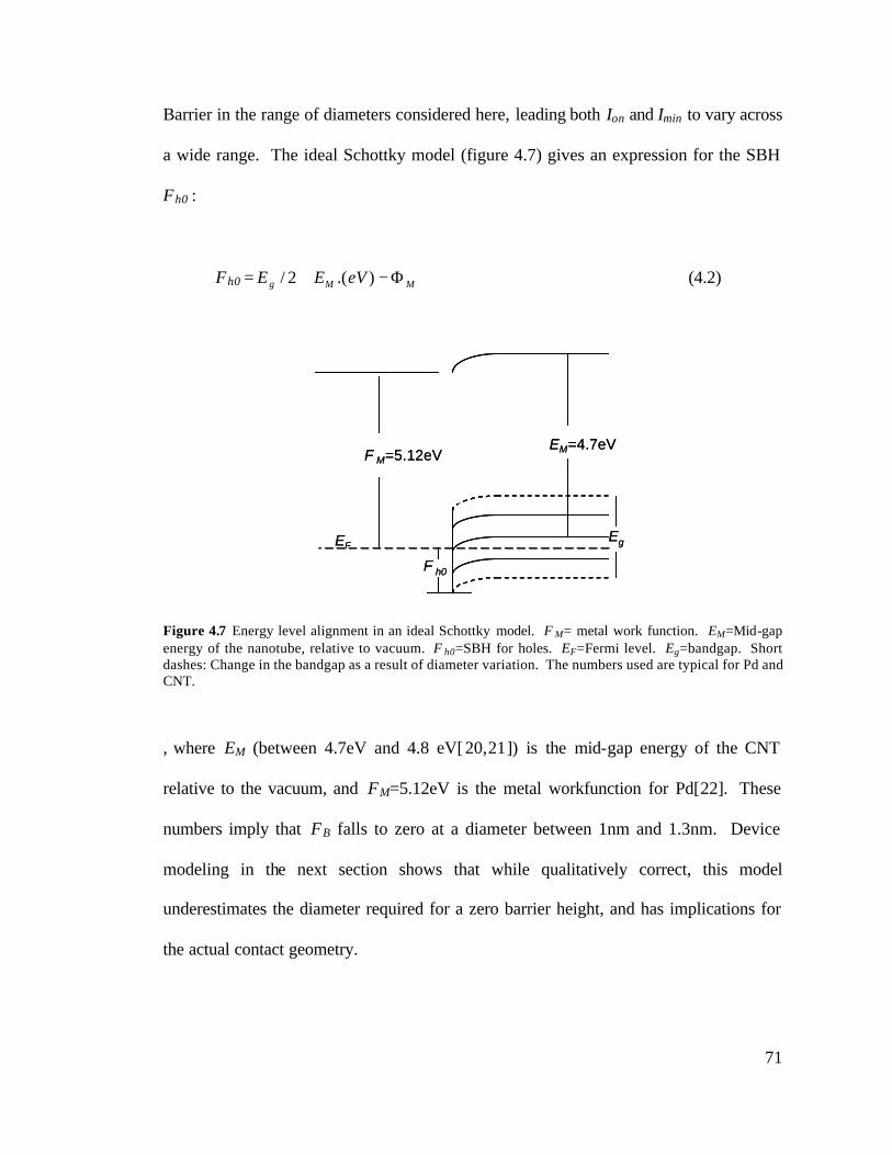
71
Barrier in the range of diameters considered here, leading both Ion and Imin to vary across
a wide range. The ideal Schottky model (figure 4.7) gives an expression for the SBH
Fh0 :
Fh0 = MMg eVEE Φ−+ ).(2/ (4.2)
EM=4.7eVF M=5.12eV
EF
F h0
Eg
EM=4.7eVF M=5.12eV
EF
F h0
Eg
Figure 4.7 Energy level alignment in an ideal Schottky model. F M= metal work function. EM=Mid-gap energy of the nanotube, relative to vacuum. F h0=SBH for holes. EF=Fermi level. Eg=bandgap. Short dashes: Change in the bandgap as a result of diameter variation. The numbers used are typical for Pd and CNT.
, where EM (between 4.7eV and 4.8 eV[20,21]) is the mid-gap energy of the CNT
relative to the vacuum, and FM=5.12eV is the metal workfunction for Pd[22]. These
numbers imply that FB falls to zero at a diameter between 1nm and 1.3nm. Device
modeling in the next section shows that while qualitatively correct, this model
underestimates the diameter required for a zero barrier height, and has implications for
the actual contact geometry.
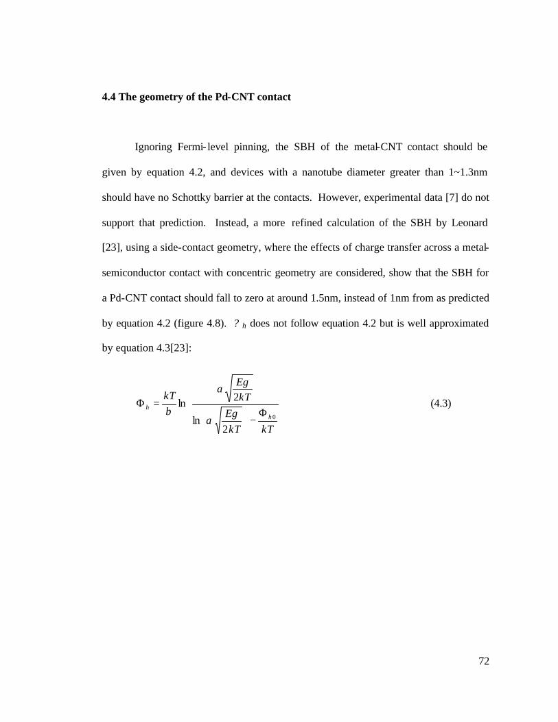
72
4.4 The geometry of the Pd-CNT contact
Ignoring Fermi- level pinning, the SBH of the metal-CNT contact should be
given by equation 4.2, and devices with a nanotube diameter greater than 1~1.3nm
should have no Schottky barrier at the contacts. However, experimental data [7] do not
support that prediction. Instead, a more refined calculation of the SBH by Leonard
[23], using a side-contact geometry, where the effects of charge transfer across a metal-
semiconductor contact with concentric geometry are considered, show that the SBH for
a Pd-CNT contact should fall to zero at around 1.5nm, instead of 1nm from as predicted
by equation 4.2 (figure 4.8). ? h does not follow equation 4.2 but is well approximated
by equation 4.3[23]:
Φ−
=Φ
kTkTEg
kTEg
kT
hh
0
2ln
2ln
α
α
β (4.3)
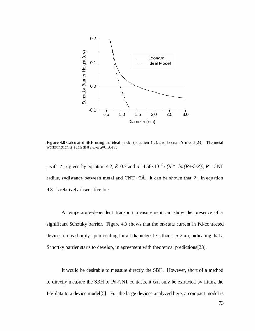
73
0.5 1.0 1.5 2.0 2.5 3.0-0.1
0.0
0.1
0.2
Sch
ottk
y B
arrie
r H
eigh
t (eV
)
Diameter (nm)
Leonard Ideal Model
Figure 4.8 Calculated SBH using the ideal model (equation 4.2), and Leonard’s model[23]. The metal workfunction is such that F M-EM=0.38eV.
, with ? h0 given by equation 4.2, ß=0.7 and a=4.58x10⁻¹¹/ (R * ln((R+s)/R)), R= CNT
radius, s=distance between metal and CNT ~3Å. It can be shown that ? h in equation
4.3 is relatively insensitive to s.
A temperature-dependent transport measurement can show the presence of a
significant Schottky barrier. Figure 4.9 shows that the on-state current in Pd-contacted
devices drops sharply upon cooling for all diameters less than 1.5-2nm, indicating that a
Schottky barrier starts to develop, in agreement with theoretical predictions[23].
It would be desirable to measure directly the SBH. However, short of a method
to directly measure the SBH of Pd-CNT contacts, it can only be extracted by fitting the
I-V data to a device model[5]. For the large devices analyzed here, a compact model is
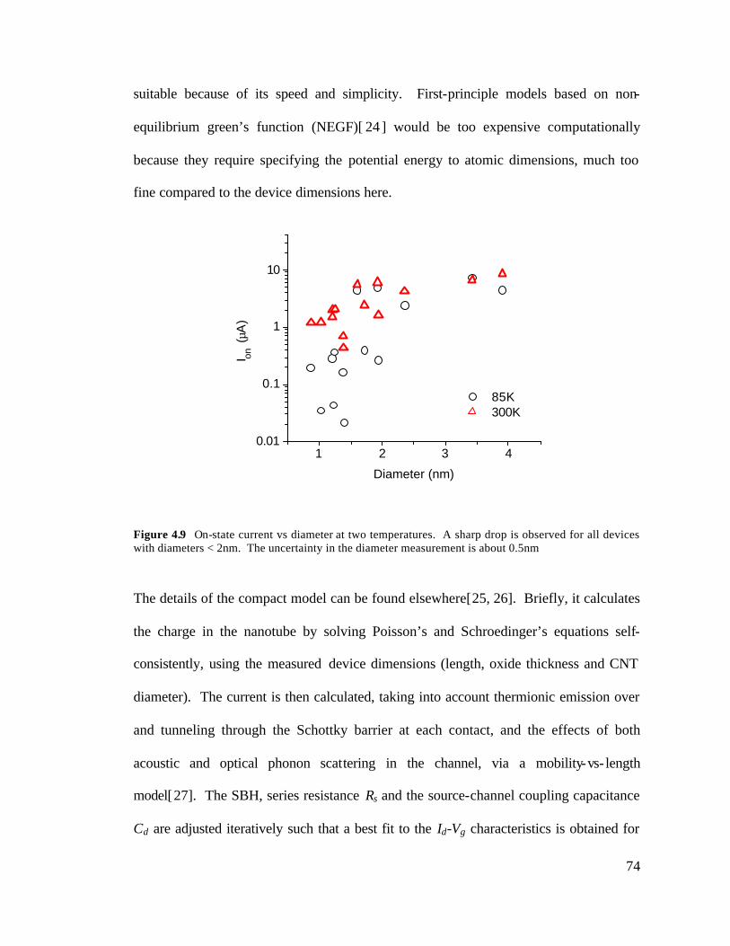
74
suitable because of its speed and simplicity. First-principle models based on non-
equilibrium green’s function (NEGF)[ 24 ] would be too expensive computationally
because they require specifying the potential energy to atomic dimensions, much too
fine compared to the device dimensions here.
1 2 3 40.01
0.1
1
10
I on (µ
A)
Diameter (nm)
85K 300K
Figure 4.9 On-state current vs diameter at two temperatures. A sharp drop is observed for all devices with diameters < 2nm. The uncertainty in the diameter measurement is about 0.5nm
The details of the compact model can be found elsewhere[25, 26]. Briefly, it calculates
the charge in the nanotube by solving Poisson’s and Schroedinger’s equations self-
consistently, using the measured device dimensions (length, oxide thickness and CNT
diameter). The current is then calculated, taking into account thermionic emission over
and tunneling through the Schottky barrier at each contact, and the effects of both
acoustic and optical phonon scattering in the channel, via a mobility-vs- length
model[27]. The SBH, series resistance Rs and the source-channel coupling capacitance
Cd are adjusted iteratively such that a best fit to the Id-Vg characteristics is obtained for
75
each device. Cd captures the drain electrode’s effect on the potential in the bulk of the
channel, and is similar to DIBL in planar MOSFETs. The results of the compact
modeling are relatively insensitive to Cd and Rs, but very sensitive to the SBH, and the
mobility [25].
Figure 4.10 shows the SBH extracted from 25 devices using compact modeling.
Although there is significant scatter, the results of compact modeling agree with the
side-contact model (equation 4.3) [23] better than the predictions from equation 4.2,
when the same contact potential FM-EM is used. Although the calculation from
equation 4.2 agrees with compact modeling when FM-EM = 0.2eV, this would imply
that the Pd workfunction is unexpectedly low, around 4.9 to 5.0eV. A better fit may
result if the actual bandgap of each device is slightly larger than Eg=0.7/d assumed in
the modeling. Taken with figure 4.9, these results strongly suggest that Leonard’s
model [23], which accounts for the overlap region between the metal and nanotube, is a
much better description of the geometry of the electrical junction. Indeed, recent 4-
probe measurements concluded that electrical current does flow under the metal
contacts[28,29], over a distance of several tens of nanometers.

76
0.2 0.4 0.6 0.8 1.0 1.2
10-3
10-2
10-1ΦM-EM=0.3eV
ΦM-EM=0.2eV
Sch
ottk
y B
arrie
r H
eigh
t (eV
)
Band Gap (eV)
Compact Modeling Leonard Ideal
Figure 4.10 Schottky Barrier Height extracted using compact modeling compared to calculations from Leonard’s model [23] (equation 4.3, solid lines) and the ideal Schottky model (equation 4.2, dashed lines). The calculations are done for two metal workfunctions F M (relative to EM, the mid-gap energy of the CNT).
Yet another evidence supporting the side-contact geometry can be deduced by
plotting Imin vs Eg. A simple formula for calculating Imin considering only the
contribution from thermionic emission is equation 4.4:
Imin = AT 2exp(-qΦe/kT) + BT 2exp(-qΦh/kT), (4.4)
The two terms of equation 4.4 are the contributions from electrons and holes. When the
current is at the minimum, the contribution from each term should be almost equal. The
prefactor A is a product of the Richardson’s constant and the junction area. A and B
should be the same for electrons and holes because the effective mass is the same. As a
result Imin should be well approximated by:
Imin = 2AT 2exp(-qΦh/kT), (4.5)
77
0.2 0.4 0.6 0.8
1
10
100
x300 I m
in (
pA)
Eg (eV)
300K 85K Leonard, ΦM-EM=0.3eV
Ideal Schottky
Figure 4.11 Imin vs band gap Eg. Lj =length of the contact. Lj=25nm is used to produce a good numerical fit. Imin from the ideal Schottky model (equation 4.2) is some 300x smaller than the data. The effective mass of the nanotube, mh*=me*=0.1m0/d(nm) [30], is used in calculating Richardson’s constant. A constant leakage current of 0.3pA is added to account for the background leakage in the semiconductor analyzer.
For each diameter (bandgap), SBH is calculated from equation 4.3. Imin calculated using
these SBH values fits well with data (figure 4.11), if one assumes that the current flows
under the contact metal over a length Lj of 25nm, illustrated in figure 4.12. However, if
the SBH is calculated from equation 4.2, Imin is some 300 times smaller than the
observed data (figure 4.11), when the same Lj=25nm is used. The length Lj =25nm
agrees with the 25nm predicted by ab-initio simulation of Nemec et al[31 ], and
consistent with conclusions from 4-probe measurements[28,29].
The strong temperature dependence of Imin shown in figure 4.11 justifies using
equation 4.4 alone for Imin, and one needs not to include contributions from tunneling.
Electrostatic calculations by Guo[32] show that the extent of the depletion region is in
78
the order of the gate oxide thickness, which is 160nm in this case. This distance is
much too large for tunneling current to be significant.
Back Gate
SiO2
Pd
CNT
Back Gate
SiO2
Pd
CNT
SiO2
Back Gate
DrainSource
Lj Lj
SiO2
Back Gate
DrainSource
Lj Lj
Figure 4.12 Definition of Lj. In calculating Imin, current is assumed to flow from the metal contact into the nanotube over the distance Lj, leading to a contact area of 2pRLj.
Although we assumed that all nanotubes are single-walled, there is a possibility
that the large-diameter nanotubes may be double-walled, or even multi-walled.
Assuming that all shells are semiconducting, the leakage current through the outer,
larger diameter shells should dominate. If a DWNT has an inner shell of 1.5nm, then
the outer shell has a diameter of 2.18nm, using an intershell distance of 0.34nm[33].
Using our simplistic model for leakage current, the outer shell would conduct 28 times
more current in the off-state then the inner shell. In addition, the coupling of the metal
to the inner shell is generally weaker. The leakage current of the devices in figure 4.11
is also much lower than what would be expected from a metallic nanotube (~10µA). As
such, if the nanotubes in question have multiple walls, they have either no metallic
shell, or the contact to these is extremely poor.
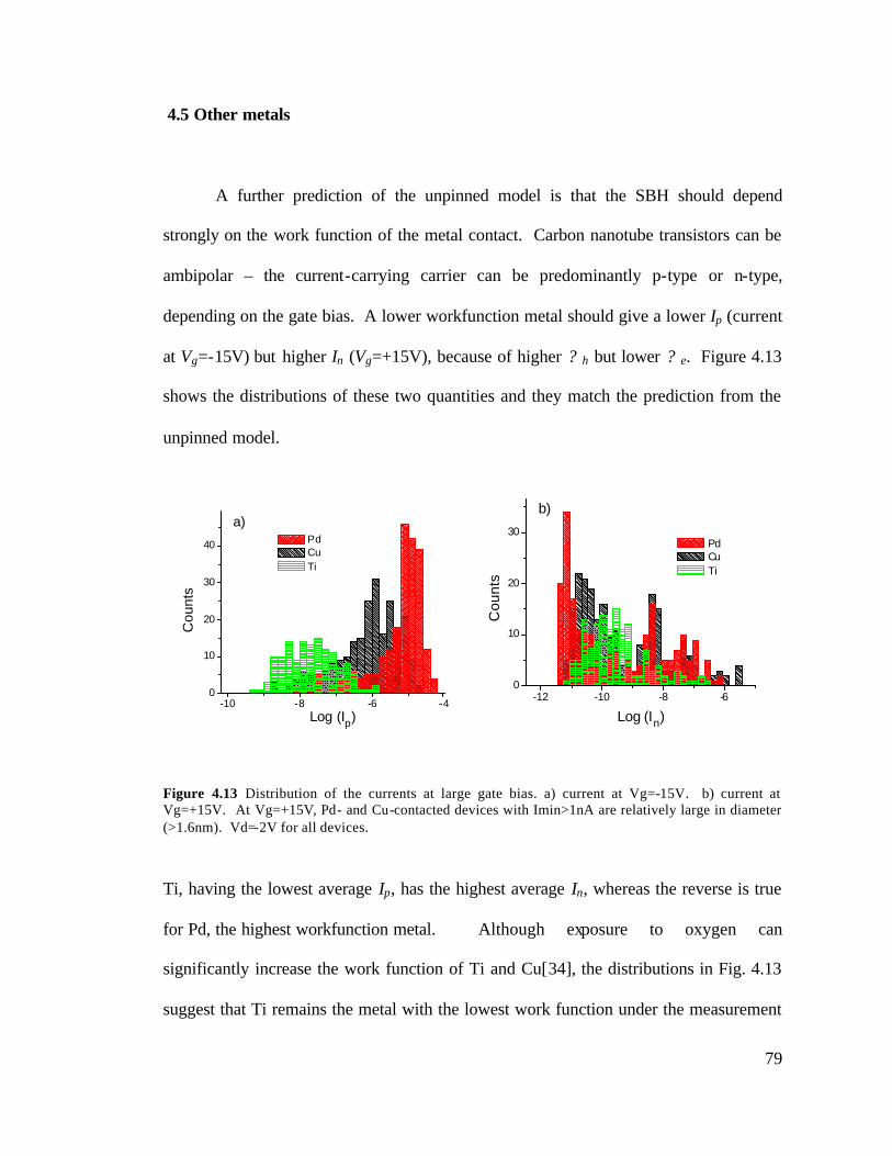
79
4.5 Other metals
A further prediction of the unpinned model is that the SBH should depend
strongly on the work function of the metal contact. Carbon nanotube transistors can be
ambipolar – the current-carrying carrier can be predominantly p-type or n-type,
depending on the gate bias. A lower workfunction metal should give a lower Ip (current
at Vg=-15V) but higher In (Vg=+15V), because of higher ? h but lower ? e. Figure 4.13
shows the distributions of these two quantities and they match the prediction from the
unpinned model.
-10 -8 -6 -40
10
20
30
40
a)
Cou
nts
Log (Ip)
Pd Cu Ti
-12 -10 -8 -60
10
20
30
b)C
ount
s
Log (In)
Pd Cu Ti
Figure 4.13 Distribution of the currents at large gate bias. a) current at Vg=-15V. b) current at Vg=+15V. At Vg=+15V, Pd- and Cu-contacted devices with Imin>1nA are relatively large in diameter (>1.6nm). Vd=-2V for all devices.
Ti, having the lowest average Ip, has the highest average In, whereas the reverse is true
for Pd, the highest workfunction metal. Although exposure to oxygen can
significantly increase the work function of Ti and Cu[34], the distributions in Fig. 4.13
suggest that Ti remains the metal with the lowest work function under the measurement
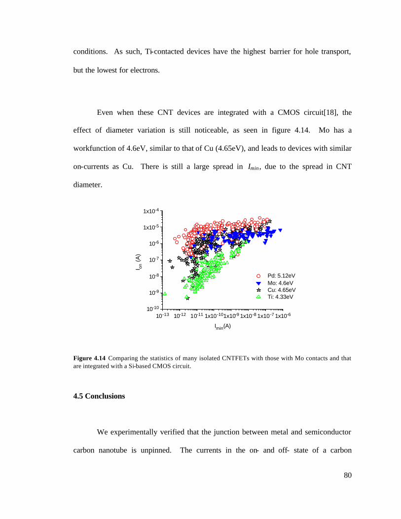
80
conditions. As such, Ti-contacted devices have the highest barrier for hole transport,
but the lowest for electrons.
Even when these CNT devices are integrated with a CMOS circuit[18], the
effect of diameter variation is still noticeable, as seen in figure 4.14. Mo has a
workfunction of 4.6eV, similar to that of Cu (4.65eV), and leads to devices with similar
on-currents as Cu. There is still a large spread in Imin, due to the spread in CNT
diameter.
10-13 10-12 10-11 1x10-101x10-9 1x10⁻⁸ 1x10 -7 1x10-610-10
10-9
10-8
10-7
10-6
1x10⁻⁵
1x10⁻⁴
I on (A
)
Imin(A)
Pd: 5.12eV Mo: 4.6eV Cu: 4.65eV Ti: 4.33eV
Figure 4.14 Comparing the statistics of many isolated CNTFETs with those with Mo contacts and that are integrated with a Si-based CMOS circuit.
4.5 Conclusions
We experimentally verified that the junction between metal and semiconductor
carbon nanotube is unpinned. The currents in the on- and off- state of a carbon

81
nanotube transistor depend sensitively on the diameter of the nanotube, as well as the
work function of the contact metal, in a way that does not require the consideration of
surface states and dipoles. Although the contacts are unpinned, the effect of geometry
can complicate the precise relationship between the band gap and the Schottky barrier
height. The results of compact modeling and temperature-dependent measurements
across devices of different CNT diameters show that a side-contact geometry is a much
better description.
For integrated circuit applications, a large-diameter nanotube with an
appropriate metal contact is desirable for its low contact resistance, and enhanced
mobility[ 35 ,36 ]. However, the off-current Imin associated with such devices will
invariably be higher. The results presented here indicate that, for small diameter
nanotubes (<1.5nm), a metal with higher work function than Pd will be needed to make
barrier-free p-type electrical contacts. Similarly, to make barrier- free n-type contacts, a
metal with a very low work function will be required. Low work function metals tend to
oxidize rapidly and are difficult to work with. The need for two distinct metal work
functions may be circumvented by using an approach involving heavily doped source
and drain[37,38]. In addition, this approach seems to have the benefit of increasing on-
state conduction while suppressing ambipolar leakage[36].
The statistical method employed in this work can also be extended to other types
of study where large variability exists. An example is the optimization of the CVD
process to control the nanotube diameter’s distribution. By measuring the on- and off-
82
state currents of a large number of nanotube devices, the diameter distribution can be
estimated rapidly. A statistical process optimization method, such as a factorial
experiment, can then be used to optimize the growth process to obtain narrowly
distributed diameters around a desired mean. The control over CNT diameter will
present a step towards the large scale integration of carbon nanotube devices.
References
[1] S. Heinze, J. Tersoff, R. Martel, V. Derycke, J. Appenzeller, Ph. Avouris, Phys. Rev.
Lett. 89, 106801 (2002)
[2 ] R. Martel, V. Derycke, C. Lavoie, J. Appenzeller, K.K. Chan, J. Tersoff, Ph.
Avouris, Phys. Rev. Lett. 87, 256805 (2001)
[3] J. Appenzeller, J. Knoch, V. Derycke, R. Martel, S. Wind, Ph. Avouris, Phys. Rev.
Lett. 89, 126801 (2002)
[4] A. Javey, J. Guo, Q. Wang, M. Lundstrom, H. Dai, Nature, 424, 654-657 (2003)
[5] Z.H. Chen, J. Appenzeller, J. Knoch, Nano Lett., 5, 1497 (2005)
[6] V. Derycke, R. Martel, J. Appenzeller, J. P. Avouris, Appl. Phys. Lett. 80, 2773-
(2002)
[7] W. Kim, A. Javey, R. Tu, J. Cao, Q. Wang, H. Dai, Appl. Phys. Lett. 87, 73101
(2005).
[8] J. Bardeen, Phys. Rev. 71, 717-727 (1947)
[9] W. Monch, J. Vac. Sci. Tech. B 6, 1270-1276 (1988)
83
[10] J. Tersoff, Phys. Rev. B 32, 6968-6971 (1985)
[11] S.M. Sze, Physics of Semiconductor Devices, 2nd edition (Wiley 1981)
[12] F. Leonard and J. Tersoff, Phys. Rev. Lett. 84, 4693-4696 (2000).
[13] R. Saito, G. Dresselhaus, M.S. Dresselhaus, Phys. Rev. B 61, 2981-2990 (2000)
[14] J. Mintmire and C.T. White, Appl. Phys. A: Solid Surf. 67, 65 (1998)
[15] S. Reich, C. Thomsen, P. Ordejon, Phys. Rev. B 65, 155411 (2002)
[16] J.W.G. Wildoer, L.C. Venema, A.G. Rinzler, R.E. Smalley, C. Dekker, Nature,
391, 59-62 (1998) ; T.W. Odom, J.-L. Huang, P. Kim, C.M. Lieber, Nature, 391, 62-65
(1998)
[17] A. Jorio, R. Saito, J.H. Hafner et al, Phys. Rev. Lett. 86, 1118-1121 (2001)
[18] Y.-C. Tseng, P. Xuan, A. Javey, R. Malloy, J. Bokor, H. Dai, Nano Lett. 4, 123-
128 (2004)
[19] K. Bosnick, N. Gabor, P. McEuen, Appl. Phys. Lett.,89, 163121 (2006)
[20] X. Cui, M. Freitag, R. Martel, L. Brus, P. Avouris, Nano Lett. 3, 783-788 (2003)
[21] S. Suzuki, C. Bower, Y. Watanabe, O. Zhou, Appl. Phys. Lett. 76, 4007-4009
(2000)
[22] CRC Handbook of Chemistry and Physics (CRC Press, Boca Raton, FL, 1986)
[23] F. Leonard and A.A. Talin, Phys. Rev. Lett., 97, 026804 (2006)
[24] J. Guo and M. Lundstrom, IEEE Trans. Elec. Dev. 49, 1897-1902 (2002)

84
[25] A. Balijepalli, S. Sinha and Y. Cao, International Symposium on Low-Power
Electronics, August 27-29, Portland, Oregon, USA (2007)
[26] S. Sinha, Y.C. Tseng, J. Bokor and Y. Cao, submitted to IEEE Transaction on
Nanotechnology
[27] J. Deng, H.S.P.Wong, IEEE Trans. Elec. Dev. 54, 3186-3194 (2007)
[28] A. Makarovski, A. Zhukov, J. Liu, G. Finkelstein, Phys. Rev. B 76, 161405(R)
(2007)
[29] G. Gunnarsson, J. Trbovic, C. Schoenenberger, arXiv:0710.0365 (unpublished)
[ 30 ] R. Saito, G. Dresselhaus, M.S. Dresselhaus, Physical Properties of Carbon
Nanotubes (Imperial College, London, 1998).
[31] N. Nemec, D. Tomanek, G. Cuniberti, Phys. Rev. Lett. 96, 076802 (2006)
[32] J. Guo, J. Wang, E. Polizzi, S. Datta, M. Lundstrom, IEEE Trans. Nanotech. 2,
329-334 (2003)
[33] S. Iijima, Nature, 354, 56 (1991)
[34] M.D. Przychowski, G.K.L. Marx, G.H. Fecher, G. Schonhense, Surf. Sci. 549, 37
(2004)
[35] X. Zhou, J.-Y. Park, S. Huang, J. Liu, P.L. Mceuen Phys. Rev. Lett. 95, 146805 (2005)
[36] V. Perebeinos, J. Tersoff, P. Avouris, Phys. Rev. Lett. 94, 086802 (2005)
[37] J. Chen, C. Klinke, A. Afzali, P. Avouris, Appl. Phys. Lett. 86, 123108 (2005)

85
[38] A. Javey, R. Tu, D.B. Farmer, J. Guo, R.G. Gordon, H. Dai, Nano Lett. 5, 345
(2005)
86
Chapter 5
Capacitance Measurement of Metal-Semiconductor Carbon Nanotube Schottky Contacts
In chapter 4 it was discussed how the Fermi- level at the contact between
semiconductor carbon nanotubes and metal is essentially unpinned. The Schottky
Barrier Height (SBH), probably the most important parameter of a metal-semiconductor
(MS) contact, was deduced using compact modeling. Chen et al[1] also extracted SBH
using a model based on non-equilibrium Green’s function (NEGF). Appenzeller used a
simple argument to qualitatively deduce the SBH from the transfer characteristics of a
nanotube transistor [2]. Nevertheless, these methods do not directly measure the SBH
of the MS contact, but rely instead on the validity of the transport and device models.
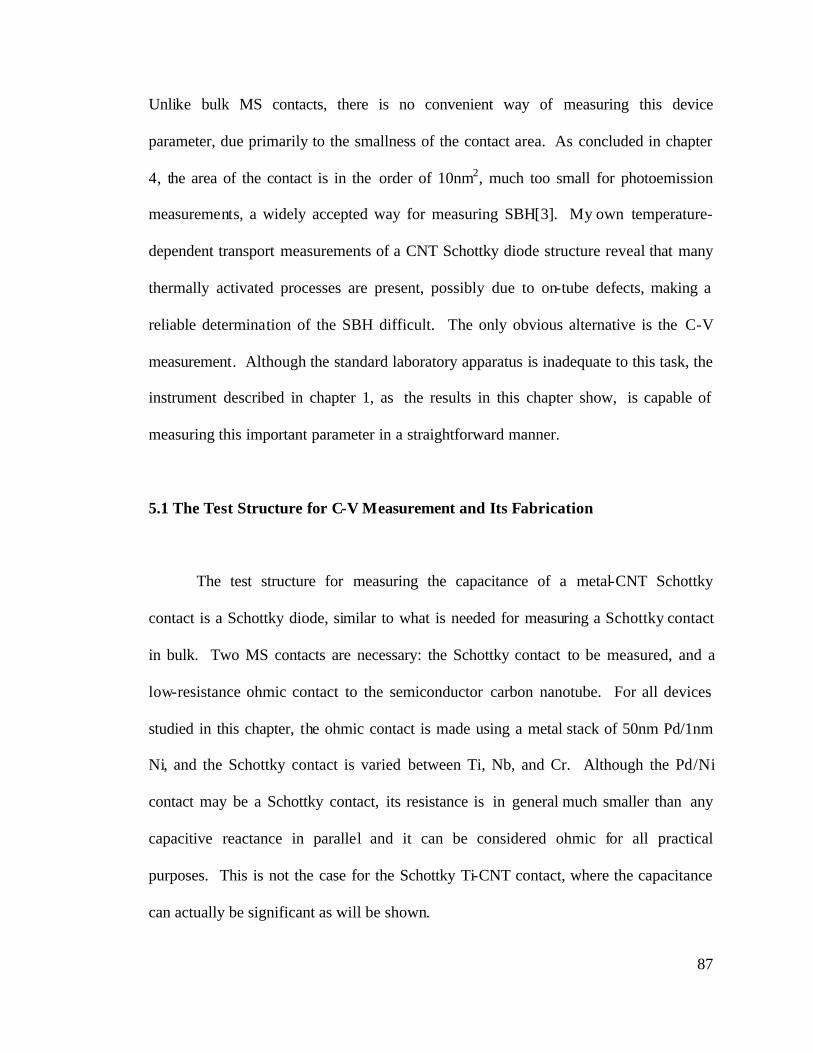
87
Unlike bulk MS contacts, there is no convenient way of measuring this device
parameter, due primarily to the smallness of the contact area. As concluded in chapter
4, the area of the contact is in the order of 10nm2, much too small for photoemission
measurements, a widely accepted way for measuring SBH[3]. My own temperature-
dependent transport measurements of a CNT Schottky diode structure reveal that many
thermally activated processes are present, possibly due to on-tube defects, making a
reliable determination of the SBH difficult. The only obvious alternative is the C-V
measurement. Although the standard laboratory apparatus is inadequate to this task, the
instrument described in chapter 1, as the results in this chapter show, is capable of
measuring this important parameter in a straightforward manner.
5.1 The Test Structure for C-V Measurement and Its Fabrication
The test structure for measuring the capacitance of a metal-CNT Schottky
contact is a Schottky diode, similar to what is needed for measuring a Schottky contact
in bulk. Two MS contacts are necessary: the Schottky contact to be measured, and a
low-resistance ohmic contact to the semiconductor carbon nanotube. For all devices
studied in this chapter, the ohmic contact is made using a metal stack of 50nm Pd/1nm
Ni, and the Schottky contact is varied between Ti, Nb, and Cr. Although the Pd/Ni
contact may be a Schottky contact, its resistance is in general much smaller than any
capacitive reactance in parallel and it can be considered ohmic for all practical
purposes. This is not the case for the Schottky Ti-CNT contact, where the capacitance
can actually be significant as will be shown.
88
The test structure is illustrated in figure 5.1. The gap between the electrodes is
about 1µm. A back gate, separated from the nanotube and the S/D contacts by 500nm
of silicon dioxide, can be used to modulate the conductivity of the bulk of the nanotube.
The background parasitic capacitance can be measured by turning off the nanotube.
The oxide needs to be thick to prevent excessive loss across the Schottky contact via
tunneling, as well as to prevent the S/D electrodes from shorting to the back gate during
wire bonding. The ultrasonic power used to create a strong mechanical bond between
the bonding pad and the wire can damage the material directly under the bond. It was
found that oxide at least 200nm thick is needed to prevent shorting the S/D electrodes to
the substrate.
Metal 2
Metal 1Metal 1
Metal 2
Metal 1Metal 1
500nmSiO2
P++
500nm500nmSiO2
P++
Figure 5.1 Test structure for C-V measurement. Only one such structure is placed on each 5mmx5mm die to reduce the background parasitic capacitance. The SEM picture shows a nanotube bridging the two dissimilar electrodes. The contact to Ti is Schottky while the contact to Pd is ohmic.
The device can also be damaged by the ultrasonic power if it is too close to the
wirebond. To reduce this problem, the bonding pads are purposely placed far away
89
(200µm) from the device, and their area minimized to reduce shunting capacitance to
ground as shown in figure 5.1. As described in chapter 1, only two devices are placed
on each die to minimize the number of floating electrodes in order to reduce the
background parasitic capacitance.
The fabrication procedures of the test structure are illustrated in figure 5.2.
Starting from a heavily boron-doped silicon wafer, wet oxidation is used to grow 500nm
of silicon dioxide. Followed is the definition of a global alignment mark, etched into
the oxide layer using buffered HF. The catalyst for growing CNTs is then deposited
and patterned using lift-off, using previously established procedures [3]. Single-walled
carbon nanotubes are then grown using CVD methods. Next, the Pd/Ni ohmic contacts
are realized by e-beam evaporation followed by lift-off. The Schottky contacts are also
realized the same way. The Ni layer is only 1nm thick and helps the Pd metal to stick to
the oxide surface. Ni has a large workfunction, and does not degrade the electrical
contact to the CNT significantly.

90
SiO2
a)
SiO2
b)
SiO2
c)
SiO2
PR2PR1
d)
SiO2
PR2PR1
e)
SiO2
f)
SiO2
a)
SiO2SiO2
a)
SiO2
b)
SiO2SiO2
b)
SiO2
c)
SiO2SiO2SiO2
c)
SiO2
PR2PR1
d)
SiO2
PR2PR1
SiO2SiO2SiO2
PR2PR1
d)
SiO2
PR2PR1
e)
SiO2
PR2PR1
SiO2SiO2SiO2
PR2PR1
e)
SiO2
f)
SiO2SiO2SiO2
f)
Figure 5.2 Fabrication procedure of the C-V test structure. a) Thermal oxidation. b) Catalyst deposition and lift-off. c) Nanotube growth. d, e) Patterning of metal 1 (Ni/Pd) and 2 (Ti, Nb or Cr) using a lift-off stack of photoresist (I-line resist on MicroChem LOR3A). f) Completed device.
Because there are only two devices per die, it is necessary to fabricate the test
devices on a wafer scale to reduce cost. However, it is impossible to insert the 4” Si
wafer, on which steps a-b in figure 5.2 are performed, into the 2.5” wide furnace tube
for growing the nanotubes. A work-around is to cut the wafers in half before inserting
them in the CNT growth furnace. The two remaining lithography steps that follow are
performed using the same GCA 6200 stepper, operated in manual mode. Although the
wafer pieces are manually loaded, alignment precision of better than 1µm is still
possible. These work-arounds are awkward, but they are necessary because of the small
furnace size for growing nanotubes. Post-processing of other bottom-up nanowires and
nanotubes on a wafer scale has the same problem, since the chambers for growing these
91
objects are often too small to accept a full wafer. Significant engineering efforts remain
in scaling up these bottom-up processes.
5.2 Transport Characteristics of Metal-Semiconductor Schottky Diodes
The transport characteristics of a Schottky diode are shown in figure 5.3. As
expected, the device is rectifying. When Vds more negative than the turn-on voltage Vn
is applied to the titanium electrode, large current starts to flow. Qualitatively, the
negative bias applied to the titanium electrode lowers the hole barrier, causing current to
flow. The negatively biased back gate electrostatically dopes the tube p-type, allowing
conduction of holes in the channel. Reverse leakage starts to develop at large positive
Vds, when the energy bands are sufficiently bent to allow band-to-band tunneling from
the valence to the conduction band of the nanotube.
Vn should be directly related to the SBH[4]. Indeed, Vn, defined here as the x-
intercept of the line tangent to the I-V curve at its steepest point, clearly decreases with
the nanotube diameter (figure 5.4), when measured in vacuum. When measured in air,
the scatter is such that no clear correlation emerges between Vn and the diameter. The
work function of Ti can be strongly affected by exposure to oxygen, and a prior work
shows that this exposure can dramatically change the SBH[5].
Gas molecules on a metal surface usually do not desorb by simply reducing the
ambient pressure to 3 x 10⁻⁵ torr, the pressure at which the I-V measurements were
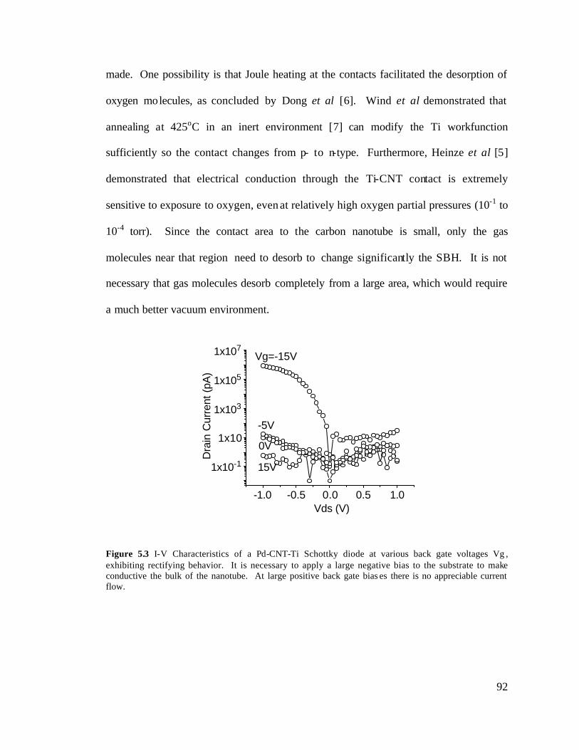
92
made. One possibility is that Joule heating at the contacts facilitated the desorption of
oxygen molecules, as concluded by Dong et al [6]. Wind et al demonstrated that
annealing at 425oC in an inert environment [7] can modify the Ti workfunction
sufficiently so the contact changes from p- to n-type. Furthermore, Heinze et al [5]
demonstrated that electrical conduction through the Ti-CNT contact is extremely
sensitive to exposure to oxygen, even at relatively high oxygen partial pressures (10-1 to
10-4 torr). Since the contact area to the carbon nanotube is small, only the gas
molecules near that region need to desorb to change significantly the SBH. It is not
necessary that gas molecules desorb completely from a large area, which would require
a much better vacuum environment.
-1.0 -0.5 0.0 0.5 1.0
1x10⁻¹
1x10
1x10³
1x10⁵
1x10⁷
15V
0V
-5V
Vg=-15V
Dra
in C
urre
nt (
pA)
Vds (V)
Figure 5.3 I-V Characteristics of a Pd-CNT-Ti Schottky diode at various back gate voltages Vg , exhibiting rectifying behavior. It is necessary to apply a large negative bias to the substrate to make conductive the bulk of the nanotube. At large positive back gate bias es there is no appreciable current flow.
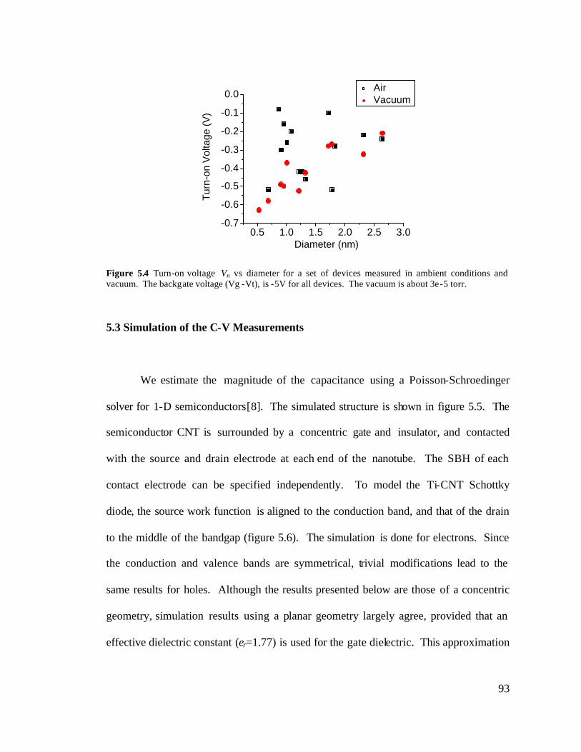
93
0.5 1.0 1.5 2.0 2.5 3.0-0.7
-0.6
-0.5
-0.4
-0.3
-0.2
-0.1
0.0
Tur
n-on
Vol
tage
(V)
Diameter (nm)
Air Vacuum
Figure 5.4 Turn-on voltage Vn vs diameter for a set of devices measured in ambient conditions and vacuum. The backgate voltage (Vg -Vt), is -5V for all devices. The vacuum is about 3e-5 torr.
5.3 Simulation of the C-V Measurements
We estimate the magnitude of the capacitance using a Poisson-Schroedinger
solver for 1-D semiconductors[8]. The simulated structure is shown in figure 5.5. The
semiconductor CNT is surrounded by a concentric gate and insulator, and contacted
with the source and drain electrode at each end of the nanotube. The SBH of each
contact electrode can be specified independently. To model the Ti-CNT Schottky
diode, the source work function is aligned to the conduction band, and that of the drain
to the middle of the bandgap (figure 5.6). The simulation is done for electrons. Since
the conduction and valence bands are symmetrical, trivial modifications lead to the
same results for holes. Although the results presented below are those of a concentric
geometry, simulation results using a planar geometry largely agree, provided that an
effective dielectric constant (er=1.77) is used for the gate dielectric. This approximation
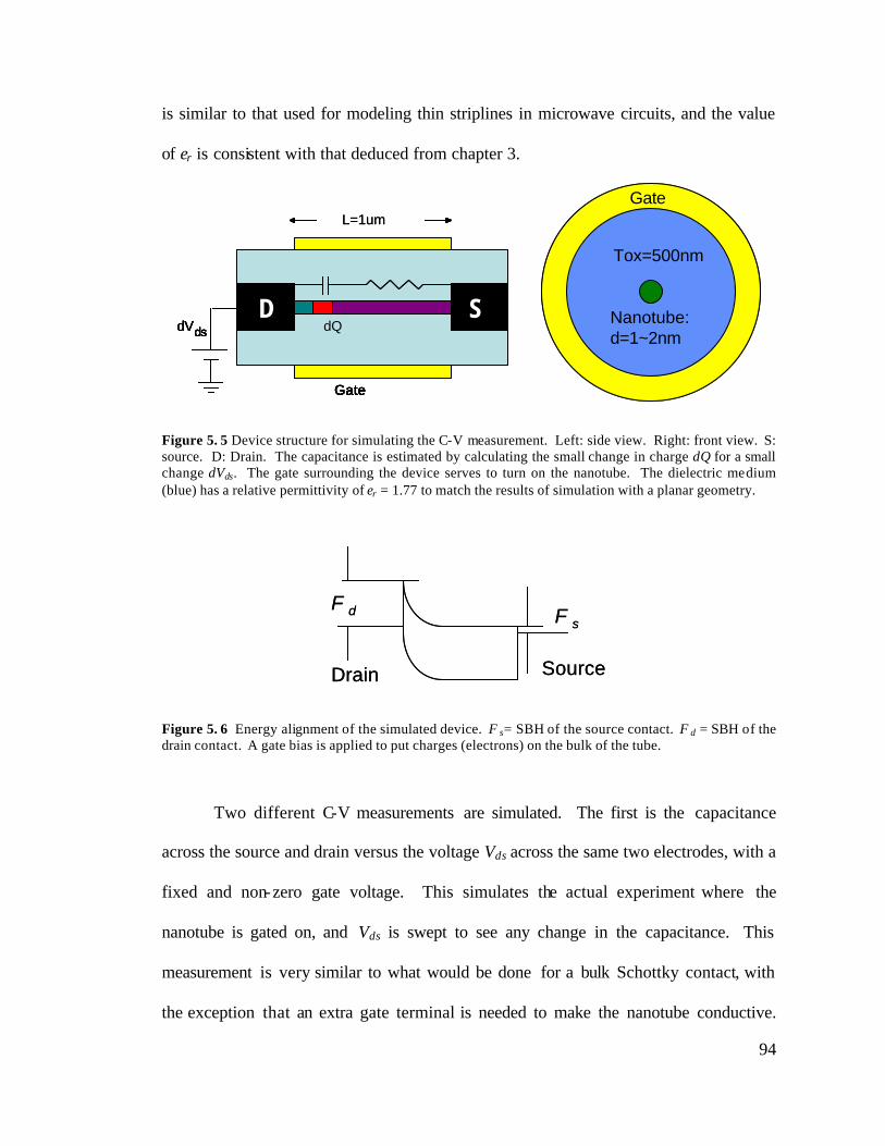
94
is similar to that used for modeling thin striplines in microwave circuits, and the value
of er is consistent with that deduced from chapter 3.
Gate
D SdQdVds
GateGate
L=1um
D SdQdVdsds
GateGate
D SdQdVds
GateGate
L=1um
D SdQdVdsds
Tox=500nm
Nanotube: d=1~2nm
Gate
Tox=500nm
Nanotube: d=1~2nm
Gate
Figure 5. 5 Device structure for simulating the C-V measurement. Left: side view. Right: front view. S: source. D: Drain. The capacitance is estimated by calculating the small change in charge dQ for a small change dVds. The gate surrounding the device serves to turn on the nanotube. The dielectric medium (blue) has a relative permittivity of er = 1.77 to match the results of simulation with a planar geometry.
Drain Source
F sF d
Drain Source
F sF d
Figure 5. 6 Energy alignment of the simulated device. F s= SBH of the source contact. F d = SBH of the drain contact. A gate bias is applied to put charges (electrons) on the bulk of the tube.
Two different C-V measurements are simulated. The first is the capacitance
across the source and drain versus the voltage Vds across the same two electrodes, with a
fixed and non-zero gate voltage. This simulates the actual experiment where the
nanotube is gated on, and Vds is swept to see any change in the capacitance. This
measurement is very similar to what would be done for a bulk Schottky contact, with
the exception that an extra gate terminal is needed to make the nanotube conductive.

95
The bias applied at the gate terminal can be thought as a way to electrostatically “dope”
the nanotube.
0 40 80 120
0.38
0.39
0.40
Pot
entia
l (V
)
Distance From Drain (nm)
Numerical Simulation Analytical Approximation Quadratic fit
Figure 5.7 Potential along the length of a nanotube with Vds applied along its length. The simu lated geometry is that shown in figure 5.5.
-0.8 -0.6 -0.4 -0.2 0.0 0.212
18
24
30
36 a)
0.60.84
1.0
1.3
1.7 3
Cap
acita
nce
(aF)
Vds (V)-0.6 -0.4 -0.2 0.0
0
10
20
30 b)
Cap
acita
nce
(aF)
Vds (V)
Planar model, best fit Eg/2+0.1, n=8
Figure 5.8 a) Simulated C-Vds curves for Schottky Junctions of various CNT diameters (in nm). The SBH is set as Eg/2+0.1 (eV). b) Comparison of the simulated C-Vds curve to a planar model ~B/(Vbi-Vds)
0.5, with fitting parameter B, and Vbi=0.67V, the SBH in the numerical simulation.

96
0 40 80 1200.30
0.35
0.40
0.45
0.50
Pot
entia
l (V
)
Distance from Drain (nm)
Vds=-0.45 Vds=-0.385V Vds=-0.32
0 40 80 120
0.000
0.006
0.012Vds=-0.45V
Vds=-0.32V
dQ (e
lect
rons
/m)
Distance from Drain (nm)
Figure 5.9 a) Potential profile near the Schottky junction for different applied bias Vds across it. b) Charge density dQ modulated by applied bias dVds across the source-drain of the Schottky junction.
As predicted from an early work on electrostatic in objects with one-dimensional
electronic density of states, potential applied across the long axis of the tube is poorly
screened and falls as ~ln(Tox/x) along the nanotube [9], where Tox is the dielectric
thickness between the gate metal and the nanotube. Figure 5.7 shows the comparison
between the results of numerical simulation, analytical approximation, and a best
quadratic fit, showing the agreement between the former two. This is expected since
the junction geometry is far from planar. Figures 5.9a-b show the potential and charge
profile as Vds is varied. As the built- in voltage is reduced and the entire device brought
close to flat-band, more charges are accumulated along the entire length of the tube,
evidence of the long screening length in the carbon nanotube. In addition, the peak
position of charge accumulation moves closer to the drain, analogous to what happens
in bulk, where the depletion width is narrowed upon canceling the built- in voltage.
The simulated C-Vds curves for different nanotube diameters and Schottky
barrier height are shown in figure 5.8a. Figure 5.8b shows that the capacitance
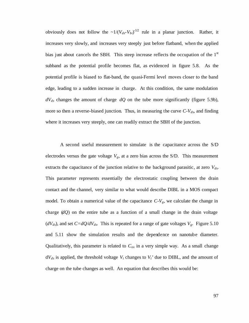
97
obviously does not follow the ~1/(Vds-Vbi)-1/2 rule in a planar junction. Rather, it
increases very slowly, and increases very steeply just before flatband, when the applied
bias just about cancels the SBH. This steep increase reflects the occupation of the 1st
subband as the potential profile becomes flat, as evidenced in figure 5.8. As the
potential profile is biased to flat-band, the quasi-Fermi level moves closer to the band
edge, leading to a sudden increase in charge. At this condition, the same modulation
dVds changes the amount of charge dQ on the tube more significantly (figure 5.9b),
more so then a reverse-biased junction. Thus, in measuring the curve C-Vds, and finding
where it increases very steeply, one can readily extract the SBH of the junction.
A second useful measurement to simulate is the capacitance across the S/D
electrodes versus the gate voltage Vg, at a zero bias across the S/D. This measurement
extracts the capacitance of the junction relative to the background parasitic, at zero Vds.
This parameter represents essentially the electrostatic coupling between the drain
contact and the channel, very similar to what would describe DIBL in a MOS compact
model. To obtain a numerical value of the capacitance C-Vg, we calculate the change in
charge (dQ) on the entire tube as a function of a small change in the drain voltage
(dVds), and set C=dQ/dVds. This is repeated for a range of gate voltages Vg. Figure 5.10
and 5.11 show the simulation results and the dependence on nanotube diameter.
Qualitatively, this parameter is related to Cox in a very simple way. As a small change
dVds is applied, the threshold voltage Vt changes to Vt’ due to DIBL, and the amount of
charge on the tube changes as well. An equation that describes this would be:
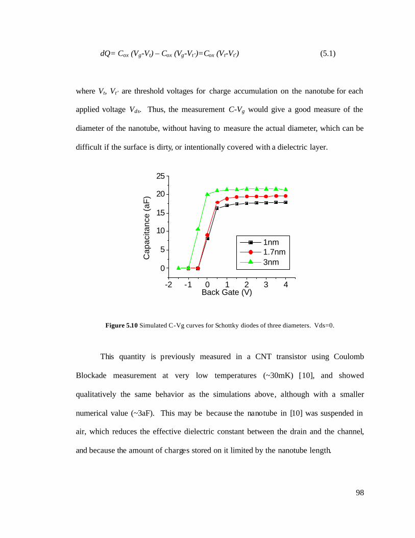
98
dQ= Cox (Vg-Vt) – Cox (Vg-Vt’)=Cox (Vt-Vt’) (5.1)
where Vt, Vt’ are threshold voltages for charge accumulation on the nanotube for each
applied voltage Vds. Thus, the measurement C-Vg would give a good measure of the
diameter of the nanotube, without having to measure the actual diameter, which can be
difficult if the surface is dirty, or intentionally covered with a dielectric layer.
-2 -1 0 1 2 3 4
0
5
10
15
20
25
Cap
acita
nce
(aF
)
Back Gate (V)
1nm 1.7nm 3nm
Figure 5.10 Simulated C-Vg curves for Schottky diodes of three diameters. Vds=0.
This quantity is previously measured in a CNT transistor using Coulomb
Blockade measurement at very low temperatures (~30mK) [10], and showed
qualitatively the same behavior as the simulations above, although with a smaller
numerical value (~3aF). This may be because the nanotube in [10] was suspended in
air, which reduces the effective dielectric constant between the drain and the channel,
and because the amount of charges stored on it limited by the nanotube length.
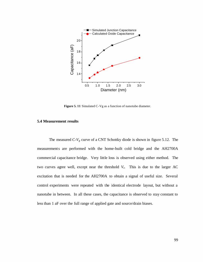
99
0.5 1.0 1.5 2.0 2.5 3.0
14
16
18
20
Cap
acita
nce
(aF
)
Diameter (nm)
Simulated Junction Capacitance Calculated Oxide Capacitance
Figure 5. 11 Simulated C-Vg as a function of nanotube diameter.
5.4 Measurement results
The measured C-Vg curve of a CNT Schottky diode is shown in figure 5.12. The
measurements are performed with the home-built cold bridge and the AH2700A
commercial capacitance bridge. Very little loss is observed using either method. The
two curves agree well, except near the threshold Vt. This is due to the larger AC
excitation that is needed for the AH2700A to obtain a signal of useful size. Several
control experiments were repeated with the identical electrode layout, but without a
nanotube in between. In all these cases, the capacitance is observed to stay constant to
less than 1 aF over the full range of applied gate and source/drain biases.
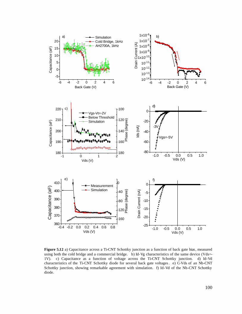
100
-6 -4 -2 0 2 4 6
-5
0
5
10
15
20a)
Cap
acita
nce
(aF
)
Back Gate (V)
Simulation Cold Bridge, 1kHz AH2700A, 1kHz
-6 -4 -2 0 2 4 610-14
10-13
10-12
10-11
1x10⁻¹⁰
1x10⁻⁹
1x10-81x10-7
1x10⁻⁶b)
Dra
in C
urre
nt (
A)
Back Gate (V)
-1 0 1 2180
190
200
210
220 c)
Cap
acita
nce
(aF
)
Vds (V)
Vgs-Vt=-2V Below Threshold Simulation
-180
-160
-140
-120
-100
Pha
se (d
egre
e)
-1.0 -0.5 0.0 0.5 1.0-80
-60
-40
-20
0d)
-3V
Vgs=-5VIds
(nA
)
Vds (V)
-0.4 -0.2 0.0 0.2 0.4 0.6 0.8360
370
380
390
400
410
Pha
se (d
egre
e)
Cap
acita
nce
(aF
)
Vds (V)
Measurement Simulation
-160
-120
-80
-40
0e)
-1.0 -0.5 0.0 0.5 1.0-25
-20
-15
-10
-5
0f)
Dra
in C
urre
nt (
nA)
Vds (V)
Figure 5.12 a) Capacitance across a Ti-CNT Schottky junction as a function of back gate bias , measured using both the cold bridge and a commercial bridge. b) Id-Vg characteristics of the same device (Vds=-1V). c) Capacitance as a function of voltage across the Ti-CNT Schottky junction. d) Id-Vd characteristics of the Ti-CNT Schottky diode for several back gate voltages . e) C-Vds of an Nb-CNT Schottky junction, showing remarkable agreement with simulation. f) Id-Vd of the Nb-CNT Schottky diode.
101
The change in capacitance with applied gate bias shown in figure 5.12a (15aF)
matches well with that expected from simulation. Comparison with the Id-Vg
characteristics shows that the abrupt increase in capacitance is due to the bulk of the
nanotube becoming conductive, and the capacitance across the junction is measured in
addition to the background. A qualitative agreement between simulation and
measurement is also observed for the C-Vds measurement is shown in figure 5.12c. As
Vds becomes more negative, beyond a certain threshold, the capacitance increases
steeply, until significant loss is encountered, as evidenced by the phase of the cold
bridge output. The rapid increase in capacitance occurs at a much smaller voltage than
that required for the device to conduct. Figure 5.12e shows the C-Vds curve of another
device, with Nb as Schottky contact, and shows a much better agreement between
simulation and experiment. The quality of the fit differs from device to device, because
many non- idealities, such as surface charges and on-tube defects, are not modeled. The
SBH found from the C-V measurements correlate well with the turn-on voltages
extracted from I-V measurement, as shown in figure 5.13a. Analyzing the room
temperature I-V curves of these same diodes, it is revealed that the ideality factor n
ranges from 1.2 to close to 3, with no clear correlation to the SBH (figure 5.13b).
Previous report on CNT Schottky diodes made with dissimilar metals[11] also reported
ideality factors between one and two. The larger n in some diodes may come from
defects near the Schottky contact. The series resistance Rs is also extracted (figure
5.13c), and it also has no clear relation to the SBH. Rs should be determined by the
bulk of the tube and the low resistance contact between the Pd metal and nanotube.
Although it has no clear relationship to the SBH, it is nevertheless small enough to have

102
no impact on the capacitance measurement. The small oscillations in the C-Vds curve
are likely due to non-monotonic variation in the charge and potential profile along the
tube, caused by neighboring charges on the oxide substrate. Such an undulating
potential profile was observed previously[12].
-0.6 -0.5 -0.4 -0.3 -0.2 -0.1 0.0
-0.8
-0.7
-0.6
-0.5
-0.4
-0.3
-0.2
Vn
(V)
-SBH using C-V (eV)
-0.6 -0.5 -0.4 -0.3 -0.2 -0.1 0.01.0
1.5
2.0
2.5
3.0b)
Idea
lity
fact
or n
-SBH (eV)
-0.6 -0.5 -0.4 -0.3 -0.2 -0.1 0.0106
107
108
c)
Rs
(Ohm
)
-SBH (eV)
Figure 5.13 a) Turn-on voltage vs SBH measured using the C-V method. b) Ideality factor vs SBH. c) Series resistance Rs vs SBH.
The C-Vg measured on 15 devices varies from 10aF to 25aF. Plotting this
change in capacitance versus the SBH extracted by the C-Vds method in figure 5.14, a
clear relationship becomes evident, where devices having larger C-Vg also has a smaller
barrier height. Using our simulator, this relationship is mostly reproduced and is shown

103
in figure 5.14. Essentially, the magnitude of the capacitance reflects simply the
diameter of the nanotube, and its apparent dependence on SBH is the result of the
unpinned junction. As evidenced in figure 5.14a-b, there is a lateral shift for the data
series of devices with a Cr contact relative to those with Ti, since Cr has a higher
workfunction (4.5eV). Devices with an Nb MS contact give very similar results to
those with Ti, since these metals have very similar work function (4.3eV for Nb vs
4.33eV for Ti).
-0.8 -0.6 -0.4 -0.2 0.00
5
10
15
20
25
30
Cap
acita
nce
(aF
)
-SBH (eV)
Ti Nb
-0.8 -0.6 -0.4 -0.2 0.00
5
10
15
20
25
30
-0.8 -0.6 -0.4 -0.2 0.00
5
10
15
20
25
30
Cap
acita
nce
(aF
)
-SBH (eV)
Cr
-0.8 -0.6 -0.4 -0.2 0.00
5
10
15
20
25
30
Figure 5.14 Capacitance C-Vg as a function of measured SBH. The open symbols are the simulated C-Vg with the Schottky Barrier Height being related to the band gap Eg as Eg/2+0.1 and Eg/2-0.1.
104
The size of the shift in the Cr data series (0.1-0.3eV) is in agreement with the
workfunction difference between Ti (Nb) and Cr, confirming once again the unpinned
nature of the MS contact. However, the magnitude of the measured C-Vg for devices
with Cr contacts differs considerably from simulation. It is possible that details of the
contact geometry are different for Cr, like the case for Pd. Further modeling, perhaps
on an ab- initio basis, is warranted to fully understand the discrepancy.
5.5 Summary and Future Work
In summary, we have developed a method to measure the capacitance across a
nanoscale Schottky contact. In our model system of Ti-CNT Schottky barrier, the
experimental results match well with the calculations based on a Poisson-Schroedinger
device simulator. We have extracted Ti-CNT Schottky barrier heights that are
consistent with the results of I-V measurements. The capacitive measurement of the
SBH across MS contacts involving different metals show once again the unpinned
nature of the contact. Nb-CNT contacts are similar to Ti, but Cr is rather different. MS
contacts with a larger metal workfunction may not fit well to the end-contact picture, as
illustrated in chapter 4.
The Pd-CNT contact, or any other low-barrier height contacts, are of particular
interest. To measure the barrier height in these systems using the C-V method would be
very difficult since these junctions are effectively very lossy capacitors. A possible way
to work around this problem would be to measure instead the barrier height of the
105
electrons, which should be large for Pd-CNT contacts. For this purpose, a reliable n-
type MS contact is then necessary, and would require the use of very low work function
metals. Sc[13] seems to be a possible solution, although there are no confirmation that
these results are reproducible. Al also has a low work function, but is only successfully
employed for large diameter nanotubes [14], and leads to Schottky diodes with large
leakage and no obvious rectifying behavior.
References
[1] Z. Chen, J.Appenzeller, J. Knoch, Y.-M. Lin, Ph. Avouris, Nano Lett. 5, 1497-1502
(2005)
[2] J. Appenzeller, M. Radosavljevic, J. Knoch, Ph. Avouris, Phys. Rev. Lett. 92,
048301, (2004)
[3] S.M. Sze, Physics of Semiconductor Devices, 2nd edition
[4] F. Leonard and J. Tersoff, Phys. Rev. Lett. 84, 4693-4696 (2000)
[5] S. Heinze, J. Tersoff, J. V. Derycke, J. Appenzeller, Ph. Avouris, Phys. Rev. Lett.
89, 106801 (2002)
[6] L.F. Dong et al, J. Appl. Phys.,101, 024320 (2007)
[7] S.J. Wind, J. Appenzeller, R. Martel, V. Derycke, P. Avouris, Appl. Phys. Lett., 80,
3817-3819 (2002)
[8] J. Guo, S. Datta, M. Lundstrom, IEEE Trans. Elect. Dev. 51, 172-177 (2004)
[9] A.A. Odintsov, Phys. Rev. Lett., 85, 150-153 (2000)
[10] P. Jarillo-Herrero, S. Sapmaz, C. Dekker, L.P. Kouwenhoven, H.S.J. van der Zant,
Nature, 429, 389-392 (2004)
106
[11] H.M. Manohara, E.W. Wong, E. Schlecht, B.D. Hunt, P.H. Siegel, Nano Letters, 5,
1469-1474 (2005)
[12] S.J. Tans and C. Dekker, Nature, 404, 834-835 (2000)
[13] Z.Y. Zhang, S.Wang, L. Ding, X.L. Liang, H.L. Xu, J. Shen, Q. Chen, R.L. Cui, Y.
Li, L.-M. Peng, Appl. Phys. Lett., 92, 133117 (2008)
[14] The author has experimented with making Al-CNT-Pd diodes, which fail to
conduct at all except for large diameter nanotubes (>4nm). Also from private
communication with A. Javey.
107
Conclusions
This work demonstrated the application of the standard capacitance-voltage
measurement technique to small devices and junctions. Using this non-destructive
characterization method, basic information about very small semiconductor junctions
were obtained in an unambiguous way. The test structure shown in chapter 1 should be
general enough for any variety of nanowires, nanotubes, and gate stack materials. In
this work, the following were studied: boron diffusion profile in a single silicon
nanowire, the metal-carbon nanotube Schottky contact, as well as the native surface of
an InAs nanowire. The information obtained from these studies confirm that 1) the
108
diffusion of boron in silicon nanowires is dominated by the interstitial-assisted
mechanism, 2) the metal-carbon nanotube Schottky contact is unpinned, and 3) electron
mobility in small InAs nanowires is limited by surface scattering.
Bottom-up, nanoscale materials hold promise in many applications. Since
surface effects often dominate the behavior of these materials, a direct method for
characterizing the surface of each individual object is important. The methods and
instrumentation described in this work show that this is possible despite of the small
area inherent to these materials. Other devices and junctions of interest that can be
studied using this technique include but are not limited to the following: abrupt PN
junction and heterojunction for tunneling transistors, organic gate dielectric for organic
electronics, and very small FinFets. The list is limited only by the imagination of the
investigator.
Although the instrument developed here was operated at cryogenic
temperatures, this method can conceivably be extended to ambient conditions, where
most devices operate. The only significant problem to be solved is the design of a
circuitry that has similar noise characteristics at room temperature. It would also be
necessary to extend the operating frequencies of this instrument to several MHz. This
next progress would expand the reach of this technique to operating conditions typical
of solid-state devices, an important point to consider in any work in this field.