introduction - stmicroelectronics · hardware design. this hardware design contributes to the...
TRANSCRIPT

August 2011 Doc ID 019009 Rev 1 1/38
AN3430Application note
How to achieve the lowest current consumptionwith STM32F2xx
IntroductionIn embedded microcontroller applications, designers and developers have specific tasks to solve and their solutions are influenced by the resources that are available and the constraints of cost, time, physical size and technology choice. At the heart of many good products, microcontrollers have a crucial influence on system power design and particularly in a brave new world that’s concerned with energy efficiency
The STM32F2xx is one of the best high-performance microcontrollers that can be used to achieve a complete embedded application with the lowest current consumption.
This application note is intended for system designers who require a software and hardware implementation overview of the low-power modes of the STM32F2xx products. It describes how to use the STM32F2xx product family in low-power mode and details the clock systems, register settings and firmware development methods in order to optimize the use of energy in applications where low power is the key.
This application note should be read in conjunction with the datasheet of the relevant STM32F2xx product and the STM32F2xx reference manual. For information on programming, erasing and protection of the internal Flash memory please refer to the STM32F2xx Flash programming manual.
The STM32F2xx datasheets, the reference and Flash programming manuals are all available from the STMicroelectronics website www.st.com.
www.st.com

Contents AN3430
2/38 Doc ID 019009 Rev 1
Contents
1 Power consumption factors . . . . . . . . . . . . . . . . . . . . . . . . . . . . . . . . . . . 3
2 STM32F2 low power design . . . . . . . . . . . . . . . . . . . . . . . . . . . . . . . . . . . 4
2.1 STM32F2 hardware design . . . . . . . . . . . . . . . . . . . . . . . . . . . . . . . . . . . . 4
2.1.1 Internal supply structure . . . . . . . . . . . . . . . . . . . . . . . . . . . . . . . . . . . . . 4
2.1.2 Hardware environment . . . . . . . . . . . . . . . . . . . . . . . . . . . . . . . . . . . . . . . 5
2.1.3 Clock management . . . . . . . . . . . . . . . . . . . . . . . . . . . . . . . . . . . . . . . . . 7
2.2 STM32F2 low power configuration . . . . . . . . . . . . . . . . . . . . . . . . . . . . . . . 9
2.2.1 Low power mode overview . . . . . . . . . . . . . . . . . . . . . . . . . . . . . . . . . . . 9
2.2.2 Power consumption and wakeup time . . . . . . . . . . . . . . . . . . . . . . . . . . 10
2.2.3 Voltage regulator configuration and impact on power consumption . . . 14
3 STM32F2 low power firmware development . . . . . . . . . . . . . . . . . . . . . 17
3.1 Firmware tips and tricks . . . . . . . . . . . . . . . . . . . . . . . . . . . . . . . . . . . . . . 17
3.1.1 Common firmware configuration . . . . . . . . . . . . . . . . . . . . . . . . . . . . . . 17
3.1.2 Special firmware configuration . . . . . . . . . . . . . . . . . . . . . . . . . . . . . . . . 20
3.1.3 Code optimization . . . . . . . . . . . . . . . . . . . . . . . . . . . . . . . . . . . . . . . . . 21
3.2 STM32F2 example of current consumption optimization . . . . . . . . . . . . . 21
3.2.1 Test environment . . . . . . . . . . . . . . . . . . . . . . . . . . . . . . . . . . . . . . . . . . 21
3.2.2 SPI_MASTER_NonOptimized firmware architecture . . . . . . . . . . . . . . . 24
3.2.3 Practical example of current optimization . . . . . . . . . . . . . . . . . . . . . . . 26
4 Conclusion . . . . . . . . . . . . . . . . . . . . . . . . . . . . . . . . . . . . . . . . . . . . . . . . 35
Appendix A Schematics . . . . . . . . . . . . . . . . . . . . . . . . . . . . . . . . . . . . . . . . . . . . . 36
Revision history . . . . . . . . . . . . . . . . . . . . . . . . . . . . . . . . . . . . . . . . . . . . . . . . . . . . 37

AN3430 Power consumption factors
Doc ID 019009 Rev 1 3/38
1 Power consumption factors
Information in this section is based on Proceedings of the IEEE, Vol.89, No.11, November 2001.
Power dissipated in CMOS circuits consists of several components as indicated in the following equation:
Ptotal = Pswitching + Pshortcircuit + Pstatic + Pleakage
The total current consumption is a sum of:
● The power required to charge or switch a capacitive load (Pswitching),
● Short circuit power consumed during output transitions of a CMOS gate as the input switches (Pshortcircuit),
● Static power consumed by the device (Pstatic),
● Leakage power consumed by the device (Pleakage).
Pswitching and Pshortcircuit components represent the dynamic power which is consumed when a device is actively changing state:
● Pswitching depends on the capacitive load, the voltage level and the system frequency: Pswitching = C * V² * f
● Pshortcircuit occurs due to the overlapped conductance of both the PMOS and NMOS transistors forming a CMOS logic gate as the input signal transitions, this current draw depends on the average current drawn during the input transition and the voltage level: Pshortcircuit = Imean * V
Pstatic and Pleakage components represent the static power consumption which is negligible compared to dynamic consumption when the clock is running.
● Pstatic is not usually a factor in pure CMOS designs, since static current is not drawn by a CMOS gate, but certain circuit structures such as sense amplifiers, voltage references, and constant current sources do exist in CMOS systems and contribute to overall power.
● Pleakage is due to leakage currents from reversed biased PN junctions associated with the source and drain of MOS transistors, as well as subthreshold conduction currents. The leakage component is proportional to device technology and temperature.
Power consumption thus depends on:
● Microcontroller unit (MCU) chip size: Technology used, number of transistors, analog features/peripherals embedded and used.
● MCU supply voltage: The amount of current used in CMOS logic is directly proportional to the voltage of the power supply squared. Thus, power consumption may be reduced by lowering the MCU supply voltage.
● Clock frequency: Power consumption may be reduced by decreasing the clock frequency when fast processing is not required by the application.
● Operating mode: Power consumption varies depending on the mode a particular application is running in (CPU on/off, oscillator on/off,...).
For an application powered by a battery, consumption is very important. Usually, average consumption should be below a certain target to ensure an optimum battery lifetime.

STM32F2 low power design AN3430
4/38 Doc ID 019009 Rev 1
2 STM32F2 low power design
2.1 STM32F2 hardware designTo introduce STM32F2xx series as a high performance and low power microcontroller in the market requires that this new generation of STM32 family come with a challenge in terms of hardware design.
This hardware design contributes to the static and dynamic current consumption of the SMT32F2 microcontroller. This is why the CMOS technology used, as well as the system design changes from one microcontroller to another depending on the final target which will be covered by this microcontroller.
2.1.1 Internal supply structure
The device requires a 1.8 V to 3.6 V operating voltage supply (VDD), except for the WLCSP package which requires 1.65 V to 3.6 V.
The real-time clock (RTC) and backup registers can be powered from the VBAT voltage when the main VDD supply is powered off.
Figure 1. Power supply overview
To retain the content of the Backup registers when VDD is turned off, the VBAT pin can be connected to an optional standby voltage supplied by a battery or another source.

AN3430 STM32F2 low power design
Doc ID 019009 Rev 1 5/38
The VBAT pin also powers the RTC unit, allowing the RTC to operate even when the main digital supply (VDD) is turned off. The switch to the VBAT supply is controlled by the power down reset (PDR) circuitry embedded in the Reset block.
An embedded regulator is used to supply the internal 1.2 V digital power, which was designed to consume the lowest current consumption needed in conjunction with low power mode used. There are three different operating modes:
● In Run mode the regulator supplies full power to the 1.2 V domain (core, memories and digital peripherals).
● In Stop mode the regulator supplies low power to the 1.2 V domain, preserving the content of registers and internal SRAM.
● In Standby mode the regulator is powered down. The content of the registers and SRAM are lost except for the standby circuitry and the backup domain.
This regulator can also be bypassed by an external one which should supply directly the MCU with 1.2V injected on Vcap1 and Vcap2 pins (refer to Section 2.2.3).
2.1.2 Hardware environment
In the real application, there are other hardware components, such as transceivers, external memories, Bluetooth chips or other microcontrollers which are connected to the STM32F2 in order to achieve the application target.
These components cause a current increase which affects both the static current consumption, depending on the PCB connection and hardware layout, and the dynamic consumption during MCU communications.
A well configured hardware design ensures the best current consumption for the final application.
For this reason we recommend following rules described in the Getting started with STM32F20xx/21xx MCU hardware development (AN3320).
Figure 2 summarizes some of these rules:

STM32F2 low power design AN3430
6/38 Doc ID 019009 Rev 1
Figure 2. Power supply hardware connection
Particular note should be paid to certain common hardware misconfigurations to avoid penalizing the total current consumption of the application; the top five are:
● REGOFF and IRROFF pin connection
Depending on the selected STM32F2xx package, these pins should be connected either to VDD or to VSS following the voltage regulator mode that user wants to

AN3430 STM32F2 low power design
Doc ID 019009 Rev 1 7/38
configure. For more details, refer to section “Voltage regulator” in STM32F20xx/21xx datasheet for details.
● Vcap_1 and Vcap_2 pin connection:
– If the user wants the voltage regulator to be active during the application, these pins must be connected to GND through 2.2uF ceramic capacitors.
– If the user wants to bypass the voltage regulator, these pins are used to inject the 1.2V supply from an external power supply. In this case, the 2.2uF capacitors should be disconnected and replaced by 100nF ceramic decoupling capacitors.
● Unused pins not connected
All unused pins must be connected to ground through a 10K pull-down resistor to avoid external disturbance on the I/Os and increase the EMC performance.
● Because clocks can be a major factor of a high current consumption, specific attention must be paid to all clock input and outputs related to the MCU or to other components on the board.
Designers should be aware that clocking other components on the board by MCU clock through one output pin (such as the MCO) will increase the current consumption due to the I/O switching frequency.
For this reason, it is up to the hardware designer to choose either routing a PCB wire from the MCO pin to other clock input components or use an external oscillator depending on the full set of clock requirements on the board (number of clock inputs and clock frequencies).
Note: Refer to Section 3.2.3: Practical example of current optimization on page 26 for information on the current consumption value versus clock output frequency.
● If no external battery is used in the application, it is highly recommended to connect VBAT externally to VDD with a 100 nF decoupling capacitor.
2.1.3 Clock management
Three different clock sources can be used to drive the system clock (SYSCLK):
● HSI oscillator clock
● HSE oscillator clock
● Main PLL (PLL) clock
The device has the two following secondary clock sources:
● 32 kHz low-speed internal RC (LSI RC), which drives the independent watchdog and, optionally, the RTC used for auto-wakeup from the stop/standby mode.
● 32.768 kHz low-speed external crystal (LSE crystal) which optionally drives the RTC clock (RTCCLK)
Each clock source can be switched on or off independently when it is not used to optimize power consumption.
Another source of energy saving is to bypass the HSE oscillator and clock the STM32F2 with an external clock source, if another clock already available on the board for other devices.

STM32F2 low power design AN3430
8/38 Doc ID 019009 Rev 1
Figure 3. STM32F2 system clock

AN3430 STM32F2 low power design
Doc ID 019009 Rev 1 9/38
The clock controller provides a high degree of flexibility to the application with regards to the choice of the external crystal or the oscillator, which are used to run the core and peripherals at the highest frequency and guarantee the appropriate frequency for peripherals that need a specific clock like Ethernet, USB high speed and full speed, I2S and SDIO.
Several prescalers are used to configure the AHB frequency, the high-speed APB (APB2) and the low-speed APB (APB1) domains. The maximum frequency of the AHB domain is 120 MHz. The maximum allowed frequency of the high-speed APB2 domain is 60 MHz. The maximum allowed frequency of the low-speed APB1 domain is 30 MHz.
There are special cases to which software and hardware developers should pay attention when computing the current consumption budget versus the system frequency:
● Minimum system clock values required by some peripherals:
– When Ethernet is used, the AHB clock frequency must be at least 25 MHz.
– When USB full speed is used, the AHB clock frequency must be at least 14.2 MHz.
– When USB high speed is used, the AHB clock frequency must be at least 30 MHz.
– When I2C is used to achieve standard mode I²C frequencies, the APB1 clock must be at least 2 MHz.
To achieve fast mode I²C frequencies, the APB1 clock must be at least 4 MHz.
To achieve 400 kHz maximum I²C fast mode, the APB1 clock must be at least 10 MHz.
● The timer clock frequencies:
– If the APB prescaler is 1, the timer clock frequencies are set to the same frequency as that of the APB domain to which the timers are connected.
– Otherwise, timer clock frequencies are set to twice (×2) the frequency of the APB domain to which the timers are connected.
This flexible system clock is one of the most important low power factors for STM32F2xx. Used efficiently, this improves the current consumption of the application by gating the unused PLL, APB domain or peripheral clocks.
2.2 STM32F2 low power configurationSTM32F2 embedded combined features of the supply controller and the power management controller provide a wide range of low power modes allowing system designers to choose the best trade-off between power consumption, wake-up time, clock frequency, wake-up sources and context backup.
2.2.1 Low power mode overview
By default, the microcontroller is in Run mode after a system or a power-on reset. Several low-power modes are available to save power when the CPU does not need to be kept running, for example when waiting for an external event. It is up to the user to select the mode that provides the best compromise between low-power consumption, short startup time and available wakeup sources.

STM32F2 low power design AN3430
10/38 Doc ID 019009 Rev 1
The devices feature three low-power modes:
● Sleep mode (Cortex-Mx core stopped, peripherals kept running)
● Stop mode (all clocks are stopped except the backup domain)
● Standby mode (1.2 V domain powered off)
Table 1. Low-power mode summary
For more information about low power modes, refer to RM0033 section “Low-power modes”.
2.2.2 Power consumption and wakeup time
This section provides observations and conclusions about the power consumption values already described in the STM32F20xx/21xx datasheet (refer to section Supply current characteristics” in the STM32F20xx/21xx datasheet for more detail about MCU conditions during measurement).
Warning: All current consumption results described in the STM32F20xx/21xx datasheet are measured using a board which only contains the MCU, boot pins (VDD,VSS) and decoupling capacitors (refer to Appendix A: Schematics).Reproducing the low power measurement tests on the Eval board results in high current consumption values due to high integration hardware components on the board.
Run mode consumption
Following are the measurement results in run mode:
Mode name Entry WakeupEffect on 1.2 V domain clocks
Effect on VDD
domain clocks
Voltage regulator
Sleep(Sleep now or Sleep-on-exit)
WFI Any interrupt CPU CLK OFFno effect on other clocks or analog
clock sources
None ONWFE Wakeup event
Stop
PDDS and LPDS bits +
SLEEPDEEP bit + WFI or WFE
Any EXTI line (configured in the EXTI registers,
internal and external lines)
All 1.2 V domain clocks OFF
HSI and HSE
oscillators OFF
ON or in low- power mode (depends on PWR power control
register (PWR_CR))
StandbyPDDS bit +
SLEEPDEEP bit + WFI or WFE
WKUP pin rising edge, RTC alarm (Alarm A or Alarm B), RTC Wakeup
event, RTC tamper event, RTC time stamp event, external reset in NRST
pin, IWDG reset
OFF

AN3430 STM32F2 low power design
Doc ID 019009 Rev 1 11/38
Figure 4. Typical current consumption vs. temperature, Run mode, code with data processing running from Flash, ART accelerator OFF, peripherals OFF
Figure 5. Typical current consumption vs. temperature, Run mode, code with data processing running from Flash memory (ART accelerator enabled) or RAM, Peripherals OFF
Figure 4 and Figure 5 present the run mode current consumption values. The only difference between these two groups of results is the ART configuration—disabled in Figure 4 and enabled in Figure 5.
STM32F2 low power design AN3430
12/38 Doc ID 019009 Rev 1
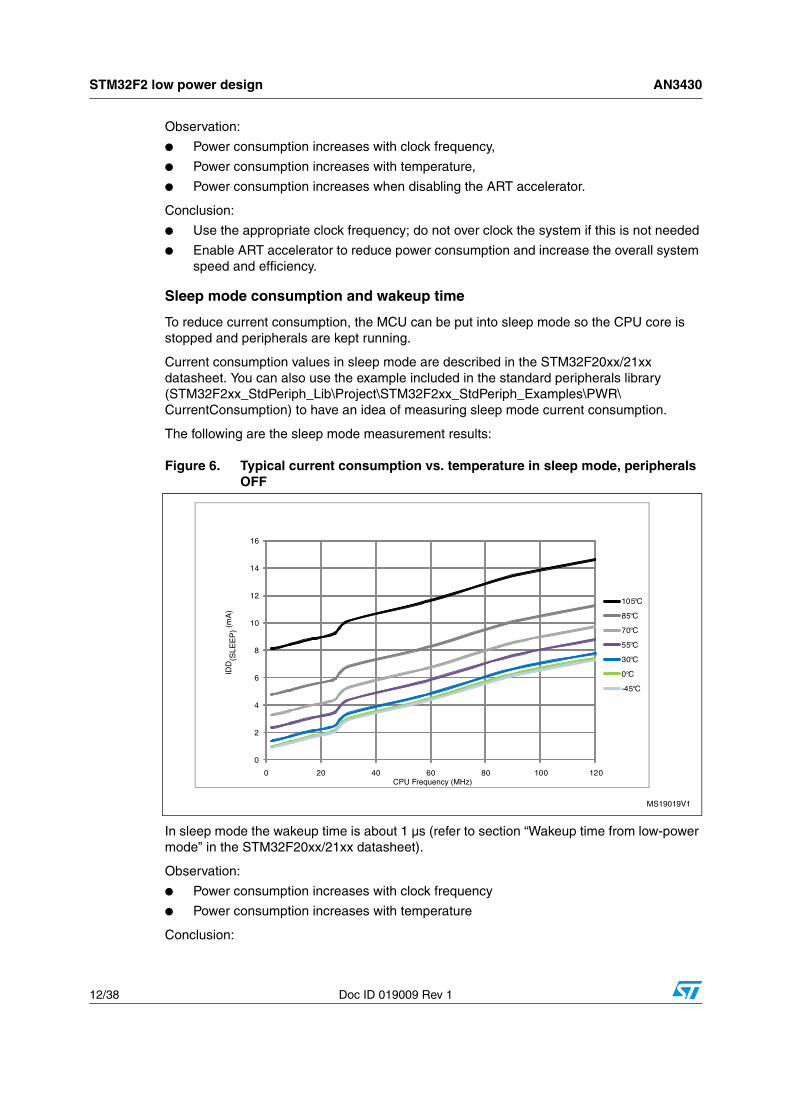
Observation:
● Power consumption increases with clock frequency,
● Power consumption increases with temperature,
● Power consumption increases when disabling the ART accelerator.
Conclusion:
● Use the appropriate clock frequency; do not over clock the system if this is not needed
● Enable ART accelerator to reduce power consumption and increase the overall system speed and efficiency.
Sleep mode consumption and wakeup time
To reduce current consumption, the MCU can be put into sleep mode so the CPU core is stopped and peripherals are kept running.
Current consumption values in sleep mode are described in the STM32F20xx/21xx datasheet. You can also use the example included in the standard peripherals library (STM32F2xx_StdPeriph_Lib\Project\STM32F2xx_StdPeriph_Examples\PWR\CurrentConsumption) to have an idea of measuring sleep mode current consumption.
The following are the sleep mode measurement results:
Figure 6. Typical current consumption vs. temperature in sleep mode, peripherals OFF
In sleep mode the wakeup time is about 1 µs (refer to section “Wakeup time from low-power mode” in the STM32F20xx/21xx datasheet).
Observation:
● Power consumption increases with clock frequency
● Power consumption increases with temperature
Conclusion:

AN3430 STM32F2 low power design
Doc ID 019009 Rev 1 13/38
Sleep mode can be used to reduce the current consumption of the application by stopping the CPU core while DMA handles the communication with the peripherals.
Stop mode consumption and wakeup time
The Stop mode is based on the Cortex-Mx deep sleep mode combined with peripheral clock gating. The voltage regulator can be configured either in run or low-power mode. In Stop mode, all clocks are stopped; the PLL, the HSI and the HSE RC oscillators are disabled. SRAM and register contents are preserved and all I/O pins keep the same state as in the Run mode.
For more information about current consumption values in stop mode, refer to section “Supply current characteristics” in the STM32F20xx/21xx datasheet.
You can also measure this current consumption using the example included in the standard peripherals library (STM32F2xx_StdPeriph_Lib\Project\ STM32F2xx_StdPeriph_Examples\ PWR\CurrentConsumption).
The following measurement results are in stop mode:
Figure 7. Typical current consumption vs. temperature in Stop mode
In stop mode, wakeup time depends on the voltage regulator and the Flash memory wakeup time. For example, if the voltage regulator is in run mode and the MCU is configured in stop mode, the wakeup time is about 13 µs. However when the voltage regulator and the Flash memory are configured in low power mode, the wakeup time increases to reach 110 µs (for more details about the wakeup time, please refer to the STM32F2xx datasheet).
Observation:
● Current consumption and wakeup time in stop mode depends on the voltage regulator configuration (run mode or low power mode) and Flash memory configuration (stop mode or deep power mode)
● A lower current consumption means a longer the wakeup time

STM32F2 low power design AN3430
14/38 Doc ID 019009 Rev 1
Standby mode consumption and wakeup time
Standby mode is based on the Cortex-Mx deep sleep mode, with the voltage regulator disabled. The 1.2 V domain is consequently powered off. The PLL, the HSI oscillator and the HSE oscillator are also switched off. SRAM and register contents are lost except for registers in the Backup domain and Standby circuitry.
For more information about current consumption values in Standby mode, refer to section “Supply current characteristics” in the STM32F20xx/21xx datasheet).
You can also measure this current consumption using the example included on the standard peripherals library (STM32F2xx_StdPeriph_Lib\Project\ STM32F2xx_StdPeriph_Examples\PWR\CurrentConsumption).
The Standby mode current consumption depends on the backup SRAM and RTC configuration, which is between 5.8 µA when both backup SRAM and RTC are enabled, and 2.5 µA when both backup SRAM and RTC are disabled (for more details about the wakeup time, please refer to the STM32F2xx datasheet).
Observation:
● Standby mode returns the lowest power consumption
● The wakeup time from Standby mode is the highest wakeup time. It is about 375 µs (refer to the section “Wakeup time from low-power mode” in the STM32F20xx/21xx datasheet)
● All I/O pins are high impedance except reset pad, and TAMPER pin if it is configured for tamper or calibration out, and the WKUP pin if it is enabled
● Wake up from standby mode means Inrush current will occur (refer to section Section 2.2.3: Voltage regulator configuration and impact on power consumption).
Conclusion:
The global wakeup time of the device can be viewed as the sum of the following:
● Wakeup time of the main voltage regulator (if it is switched off during the low-power mode)
● Stabilization time of the oscillator (if it is switched off during the low-power mode)
● Wakeup time of the Flash memory (if it is switched off during the low-power mode)
● Interrupt latency for the wake up event trigger
The results above shows the trade-off between consumption and wakeup time in the STM32F2. Generally, the lower the power consumption is, the longer the wakeup time. You should therefore try to find the best trade-off according to the application constraints.
2.2.3 Voltage regulator configuration and impact on power consumption
As described in Section 2.1.2 on page 5, the voltage regulator can be configured to be ON or OFF, depending on the package used (REGOFF and IRROFF pin availability) and the hardware environment (Vcap1 and Vcap2 pins configuration).

AN3430 STM32F2 low power design
Doc ID 019009 Rev 1 15/38
Voltage regulator ON
When the voltage regulator is ON the hardware environment is set:
● Depending on the package, IRROFF and REGOFF pin (if available on the used package) are set to VSS, (see section “Voltage regulator” in the STM32F20xx/21xx datasheet)
● Vcap_1 and Vcap_2 pins are connected to GND through a 2.2uF ceramic capacitor
When the voltage regulator is ON, the Inrush current affects the dynamic power consumption at Power ON, and also and when the CPU wakes up from Standby mode.
In fact, the Inrush current is coming from the 2*2.2 µF Vcap capacitors, which are discharged when the voltage regulator is powered down (power off or Standby mode). These capacitors are charged at Power ON or when waking up from Standby mode. This results in the Inrush current reaching up to 200 mA (maximum) in a short time (about 30 µs).
To measure the Inrush current, place a current probe between one Vcap capacitor and the ground, then multiply the result by 2 (there are two Vcap capacitors drawing energy).
Figure 8 shows the Inrush current:
Figure 8. Inrush current div 2 (50mA/1DIV)
This parameter is described in the datasheet as Inrush current on voltage regulator (see the STM32F20xx/21xx datasheet Table 14 for more information).
Observation:
● The Inrush current does not affect the average current consumption of the application because the Inrush time is too short in relation to the global application time.
● When the voltage regulator is ON, all the equivalent power relative to ddp = (3.3 V - 1.2 V) is dissipated.

STM32F2 low power design AN3430
16/38 Doc ID 019009 Rev 1
Note: Important: The Inrush current of the STM32F2 is maximum 5.3 µC, and it is about 10 times less than USB compliance Inrush current which is specified at 5 V as 50 µC maximum.
Voltage regulator OFF
When the voltage regulator is OFF the hardware environment is set:
● Depending on the package IRROFF and/or REGOFF pin (if available on the used package) are set to VDD, (see section “Voltage regulator” in the STM32F20xx/21xx datasheet)
● Vcap_1 and Vcap_2 pins are connected to the external 1.2 V power supply and these pins must be decoupled with 2 * 100 nF ceramic capacitors
Observation:
● Standby mode is not allowed because 1.2V domain is controlled by the external power supply injected on Vcap pins.
● There is no Inrush current when the voltage regulator is bypassed.
● In this mode, there is no power dissipated by the voltage regulator.
● When bypassing the voltage regulator, for example we can save about 1/2 of the power which is wasted if the voltage regulator is active.

AN3430 STM32F2 low power firmware development
Doc ID 019009 Rev 1 17/38
3 STM32F2 low power firmware development
Software plays an important role in achieving the lowest current consumption. Code needs to be optimized, not just in terms of functionality but also with respect to energy efficiency. Software has perhaps never really been formally identified as an ‘energy drain’ and it needs to be. Every clock cycle and line of code consumes energy and this needs to be minimized to achieve the best energy efficiency.
3.1 Firmware tips and tricks
3.1.1 Common firmware configuration
ART configuration
The ART Accelerator™ is a memory accelerator which is optimized for STM32 ARM® Cortex™-Mx processors. It balances the inherent performance advantage of the ARM Cortex-Mx over Flash memory technologies, which normally requires the processor to wait for the Flash memory at higher operating frequencies. Thanks to the ART Accelerator™, the CPU can operate up to 120 MHz without wait states, thereby increasing the overall system speed and efficiency.
To release the full processor 150 DMIPS performance at this frequency, the accelerator implements an instruction prefetch queue and instruction/data, which enables program execution from Flash memory at up to 120 MHz without wait states.
To avoid extra power consumption it is recommended to configure the ART as follows:
/* Disable prefetch buffer */
FLASH->ACR & = ~FLASH_ACR_PRFTEN;
/* Enable flash instruction cache */
FLASH->ACR |= FLASH_ACR_ICEN;
/* Enable flash data cache */
FLASH->ACR |= FLASH_ACR_DCEN;
The system performance can be adjusted to the current needs. This can be done either from start, according to performance estimations, or on-the-fly on a running system to adjust the performance to the current condition. In this way the prefetch can be enabled or disabled on-the-fly depending on user needs.
Disabling the prefetch buffer avoids extra Flash access that consumes 20 mA for 128-bit line fetching.

STM32F2 low power firmware development AN3430
18/38 Doc ID 019009 Rev 1
System clock configuration
The power consumption in Run mode can be reduced by the following means:
● Slowing down the system clocks
● Gating the clocks to the APBx and AHBx peripherals when they are unused
● In Run mode, stopping the HCLKx and PCLKx for individual peripherals and memories at any time to reduce power consumption
● Estimating the clock speed of the peripheral buses during prototyping by calculating the needed bandwidth and testing the settings on the hardware. The adjustment of the clocks on-the-fly is not recommended as all clock settings for modules on the bus need to be recalculated.
● Not over clocking the CPU if this is not needed on the application
● Using the STM32F2xx_Clock_Configuration.xls tool in expert mode. When it is used in wizard mode, is not optimized for current consumption.
● When the STM32F2xx_Clock_Configuration.xls tool is used in expert mode to generate system and peripherals clocks, take care to choose the correct clock configuration and to set the prescalers to the max. value on the associated PLLs of the peripherals that are not used (see Figure 9).
For example: Using the STM32F2xx_Clock_Configuration.xls tool to configure the system clock of the application. In the user application, the following peripherals are not used: USB OTG FS, RNG, SDIO, I2S and all those clocked by PCLK1. The application only requires PCLK2 clocked at 60 MHz.
Figure 9. Example of optimized clock configuration
To summarize the example of optimizing the system clock:
● Set the system clock to the value needed in your application (60MHz in this application). This clock value can be achieved with different combinations of prescalers,

AN3430 STM32F2 low power firmware development
Doc ID 019009 Rev 1 19/38
but the best way is to set SYSCLK to 60 MHz and the AHB prescaler to 1 as shown in Figure 9.
● Disable I2S clock, because it is not needed in the application
● Set PLL_Q prescaler to its maximum value, because USB OTG FS, RNG, SDIO are not used on this application
● Set APB1 prescaler to its maximum value because all PCLK1 peripherals are not used in this application
I/O configuration
After a reset, all STM32F2 pins are configured as inputs except some JTAG pins such as PA15 JTDI with pull-up, PA14 JTCK with pull-down and PA13 JTMS with pull-up. This has an impact on the power consumption of the device in the different power save modes because in input mode I/O pins are very sensible to external noise.
To set the device in the lowest possible power mode, all pins should be configured as analog input (AIN), because in analog configuration the Schmitt trigger input is deactivated, providing zero consumption for each I/O pin.
We recommend configuring the I/Os as follows:
● At the startup of the application:
– Enable all GPIO clocks
– Configure all I/Os in analog input mode
– Disable all GPIO clocks
● In the main application:
– Enable the required GPIO clock
– Configure the required I/Os on the application
● I/O configuration trick:
– If the user application just needs the I/Os to configure it as a peripheral alternate function in order to output or input signals (no read or write from/to GPIO registers), we recommend disabling the associated GPIO clock of the used I/Os after configuration. In this case I/O signals are still available and we optimize the GPIO current consumption by disabling its clock.
● I/O toggling frequency:
– When configuring the I/O, pay specific attention to the I/O speed value configured in OSPEEDR (2 MHz, 10 MHz, 25 MHz, 50 MHz and 100 MHz). Current consumption is as high as the I/O toggling frequency, so, to optimize current consumption, OSPEEDR should be configured with the lowest possible value.
Table 2. Example of I/O toggling frequency current consumption versus I/O load (VDD=3.3 V, I/O speed= 50 MHz)
I/O toggling fequency/load
30 MHz 15 MHz 3.75 MHz 1.85 MHz
Pin disconnected(pad cut)(1) 2.17 mA 1.55 mA 0.98 mA 0.7 mA
CS(2) 2.93 mA 2.1 mA 1.1 mA 0.77 mA
10 pF + CS 3.97 mA 2.73 mA 1.23 mA 0.83 mA
STM32F2 low power firmware development AN3430
20/38 Doc ID 019009 Rev 1
Table 2 shows the current consumption of a pin (such as the MCO or SPI SCK pin) that continuously switches at a specific frequency.
3.1.2 Special firmware configuration
ADC application
● The ADC can be also a source of current draw during the Stop mode, unless it is disabled before entering it. To disable it, write the ADON bit in the ADC_CR2 register to 0.
● In run mode, ADC can be configured in power-down mode by clearing the ADON bit. In this mode the ADC consumes almost no power (only a few µA).
● In the application controlling the battery threshold through ADC_IN18 input channel, when setting VBATE bit in ADC_CCR register in run mode, there is an extra current consumption seen in Vbat pin. As a consequence, this may impact the battery life time. In fact, as the VBAT voltage could be higher than VDDA, to ensure the correct operation of the ADC, the VBAT pin is internally connected to a bridge divider by 2. This bridge is automatically enabled when VBATE is set, to connect VBAT/2 to the ADC1_IN18 input channel. To prevent any unwanted consumption on the battery, we recommend enabling the bridge divider only when needed, for ADC conversion.
DAC application
● The DAC can be also a source of current draw during the Stop mode, unless it is disabled before entering it. To disable it, write the ENx bit in the DAC_CR register to 0
● Once the DAC channelx is enabled, the corresponding GPIO pin (PA4 or PA5) is automatically connected to the analog converter output (DAC_OUTx). In order to avoid parasitic consumption, the PA4 or PA5 pin should first be configured to analog (AIN).
RTC application
To clock the RTC registers, a programmable prescaler is split into 2 prescalers a 7-bit asynchronous prescaler and a 13-bit synchronous prescaler.
When both prescalers are used, we recommend configuring the asynchronous prescaler to a high value to minimize consumption.
Peripherals low power mode
There are independent low power modes for certain peripherals like the USB, Ethernet, bxCAN. When the CPU is in run mode, these peripherals can enter low power mode
33 pF + CS 4.89 mA 3.7 mA 1.52 mA 0.96 mA
47 pF + CS 5.85 mA 4.14 mA 1.67 mA 1.03 mA
1. The pin is externally removed from the LQFP176 package to avoid the pad capacitance.
2. CS: pad, board and PCB layout equivalent capacitance.
Table 2. Example of I/O toggling frequency current consumption versus I/O load (VDD=3.3 V, I/O speed= 50 MHz) (continued)
I/O toggling fequency/load
30 MHz 15 MHz 3.75 MHz 1.85 MHz

AN3430 STM32F2 low power firmware development
Doc ID 019009 Rev 1 21/38
independently and then wake up automatically when needed. For more information, refer to the STM32F2xx reference manual (RM0033).
MCO pin usage
The outputting clock on MCO pin is one of the important sources of over current consumption (same phenomenon as I/O toggling frequency), and developers should be aware that MCO pin toggling at high frequency will impact the total current consumption of the application.
However, the outputting clock on MCO pin remains an important feature for debug purpose.
Memory software remap
To boost the performance, the system configuration controller (SYSCFG) can be configured to remap the memory accessible in the code area. In remap mode the CPU can access the external memory via the ICode bus instead of the system bus, which increases the global application performance.
Developers should be aware that increasing performance by configuring the software remap will increase the current draw.
3.1.3 Code optimization
As a development process proceeds, code size naturally increases and optimizing it for energy efficiency becomes a much harder and time-consuming task.
Software developers must ensure the best firmware size and speed optimization during development process in order to achieve the lowest current consumption.
Optimizing firmware for current consumption can be achieved via:
● Firmware development, which should be optimized with only the required instructions. We recommend making direct read/write to/from registers instead of using firmware which contains many loops and instructions that can be a source of extra current consumption.
● Using toolchain optimization options to save more energy.
3.2 STM32F2 example of current consumption optimizationThis section is based on practical implementation of the low power firmware tips and tricks described above.
3.2.1 Test environment
This section gives details on the hardware, software and tools environment used to measure the STM32F2 current consumption.
Application requirements
Firstly we develop an application based on a set of application requirements defined for the purpose of giving a practical example. Then in a second step we optimize the application to achieve the lowest current consumption while still respecting the given requirements.

STM32F2 low power firmware development AN3430
22/38 Doc ID 019009 Rev 1
The application requirements are:
● SPI communication between two STM32F2 MCUs
● SPI must be configured in 16-bit data format
● SPI1 must be used
● Each 20 ms, 1024 bytes are transferred from SPI1 slave to SPI1 master
● Output clock available on MCO2 pin for debug purpose
The following figure summarizes the application requirements:
Figure 10. Application architecture and requirements
Note: The buffer size referred to in Figure 10, is 1022 bytes. In this case the total number of data bytes transferred from slave to master is 1024 bytes = 2 bytes (buffer size) + 1022 bytes (useful data).
Requirements analysis
In this application we have to transfer 1024 bytes every 20 ms, in this case the SPI baudrate needs to be higher than (1024 * 8)/20 ms = 410 Kbit/s.
We then analyze the possible baudrates in the range between 468 Kbit/s and 7.5 Mbit/s and then consider how this can impact the current consumption.
● At 468 Kbit/s, the 1024 bytes will be transferred within 17.5 ms
● At 7.5 Mbit/s, the 1024 bytes will be transferred within 1 ms
Figure 11 explains the SPI transfer in more detail.
SPI1_Master SPI1_Slave
SPI1 configuration SPI1 configuration
SPI1 sends one dummy data to slave
SPI1 sends the buffer size tobe transmitted to the master
SPI1 receives the buffer size from the slave
SPI1 sends a full buffer of dummy data to the slave
SPI1 sends the buffer of useful data to the master
SPI1 receives buffer of usefuldata from the slave
This process
Mustbe doneby polling
is repeatedevery 20 ms

AN3430 STM32F2 low power firmware development
Doc ID 019009 Rev 1 23/38
Figure 11. SPI transfer diagram
Hardware environment
● The first board (SPI1 Master) is a board with an STM32F217IGH6 MCU and only decoupling capacitors, boot pins and JTAG interface mounted on the board.
● The second board (SPI1 Slave) is identical to the first board.
● HSE crystal oscillator = 25 MHz
Note: All current consumption results described on the rest of this application note are measured using a generic board containing only the MCU, Boot pins (VDD,VSS) and decoupling capacitors. Please refer to Appendix A: Schematics on page 36.
The hardware connection between the two STM32F2 board is described in Figure 12:
MS19825V1V1
0
0
20 40 60ms
ms
20 40 60
SPI idle
SPI transfer
SPI idle
SPI transfer
17.5
7.5 Mbits/s
468 Kbits/s
STM32F2 low power firmware development AN3430
24/38 Doc ID 019009 Rev 1
Figure 12. SPI hardware connection between two boards
Note: 1 The connection between the pins should use a short wires and a common ground.
2 The two boards are supplied by an external power supply fixed at 3.3 V and the GND of the two power supply outputs must be linked together.
3 Temperature: 25°C
Software toolchain
All tests and results presented on the following sections are based on the EWARv6.21 toolchain.
Note: Using other toolchains may result other current consumption values.
Firmware deliverables
A firmware package is associated with this application note, which contains three projects:
● “SPI_MASTER_NonOptimized“: which is the non optimized project developed without implementing the low power tips and tricks. This project is used as the baseline for optimizing the current consumption, making investigations and reaching conclusions from the practical tests and results.
● “SPI_MASTER_Optimized“: which is the optimized project, meeting the same application requirements as the first firmware project, but with the lowest possible current consumption.
● “SPI_SLAVE“: which is the project running on the second STM32F2 board and communicating with the SPI1 on the first STM32F2 board.
In the rest of this application note, use on the “SPI_MASTER_NonOptimized“ project as a starting point and modify it step by step to see how this impacts the current consumption.
3.2.2 SPI_MASTER_NonOptimized firmware architecture
As we are going to use the “SPI_MASTER_NonOptimized“ project as a base for optimizing the STM32F2 current consumption, we need to understand the firmware architecture which must conform to the application requirements described in Section 3.2.1 on page 21.
MS19826V1
SPI master device SPI slave device
SCKMOSIMISO
GNDGND
Board A Board BA
DDV

AN3430 STM32F2 low power firmware development
Doc ID 019009 Rev 1 25/38
The “SPI_MASTER_NonOptimized” folder contains all the subdirectories and files that make up the core of the application example:
● stm32f2xx_conf.h: contains the configuration includes of peripherals,
● stm32f2xx_it.h: contains the headers of the interrupt handlers,
● main.c: contains the main program body
● stm32f2xx_it.c: contains the interrupt service routines, in this case it contains the SysTick interrupt which is generated every 20 ms to trigger the SPI communication.
● system_stm32f2xx.c: contains the system clock configuration for STM32F2xx.
● EWARM: contains the project for the EWARM toolchain.
Figure 13 describes the firmware architecture in more detail:
Figure 13. SPI_MASTER_NonOptimized firmware architecture
Note: In main.c file there are two defines:
#define MAIN_POLLING: This define must be used when optimizing the firmware from step 1 to step 7 and at step 9 (refer to Section 3.2.3).
#define MAIN_DMA: This define must be used when optimizing the firmware at step 8 (refer to Section 3.2.3).
SPI1 configuration
SPI1 sends dummy data to slave
SPI1 receives the buffer size from the slave
SPI1 sends buffer size (1022 bytes) dummy data to the slave
SPI1 receives buffer size (1022 bytes) useful data from the slave
Start
Configure SysTick to generate an interrupt every 20 ms
End
Mustbe doneby polling
(application requirement)
This processis repeatedevery 20 ms
(applicationrequirement)

STM32F2 low power firmware development AN3430
26/38 Doc ID 019009 Rev 1
3.2.3 Practical example of current optimization
This section describes the sequence and the step by step modifications to apply to the “SPI_MASTER_NonOptimized“ project in order to achieve the lowest current consumption.
Note: Important: In all the following steps, unless explicitly mentioned, the EWARM optimization is set to “none”.
Note: In all the following steps, always reset board B (SPI slave) before running the firmware of board A (SPI master).
Step1:
● Be sure that the SPI pin connections as well as the external power supply of the two boards is correctly done as described in Figure 12.
● Load the “SPI_SLAVE“ project on board B.
● Comment (//#define MAIN_DMA) and uncomment (#define MAIN_POLLING) in the main.c file of the “SPI_MASTER_NonOptimized” project then load the code in board A.
You can experiment with changing the SPI baudrate and see the current consumption results.
Note: You can find the system clock configuration in the system_stm32f2xx.c file: HCLK = 60 MHz, APB2 = 60 MHz and APB1= 30 MHz, system running from HSE = 25 MHz and the ART is disabled.
Observation:
In this case, the best configuration in terms of current consumption is to set the SPI prescaler to 8.
Step 2:
As described on Section 2.2.2, enabling the ART reduces the current consumption, so now let’s enable the ART and repeat the same tests as in step 1.
To enable the ART please use the following code:
/* Enable prefetch buffer */ FLASH->ACR |= FLASH_ACR_PRFTEN;
/* Enable flash instruction cache */ FLASH->ACR |= FLASH_ACR_ICEN;
/* Enable flash data cache */ FLASH->ACR |= FLASH_ACR_DCEN;
Please add this code in the “system_stm32f2xx.c” file in the “SetSysClock“ function after the following line:
FLASH->ACR = FLASH_ACR_LATENCY_1WS;
Table 3. Step1 current consumption results
SPI prescaler (baudrate)(1)
1. SPI1 is clocked by APB2 = 60 MHz.
Current consumption
Pres = 8 (baudrate 60/8 = 7.5 Mbit/s) 28.7 mA
Pres = 16 (baudrate 60/16 = 3.75 Mbit/s) 29 mA
Pres = 64 (baudrate 60/64 = 937 Kbit/s) 30.5 mA
Pres = 128 (baudrate 60/128 = 468 Kbit/s) 30.6 mA

AN3430 STM32F2 low power firmware development
Doc ID 019009 Rev 1 27/38
Observations:
● Enabling the ART reduces the total current consumption by about half
● Decreasing the SPI baudrate slightly decreases the current consumption.
● In this case, the best configuration in terms of current consumption is to set SPI prescaler to 128.
Step 3:
In the application requirements, SPI1 is used with a maximum baudrate of 7.5 Mbit/s. In this step, we optimize the system clock as described on System clock configuration on page 18.
To optimize the STM32F2 system clock, the “STM32F2xx_Clock_Configuration.xls” tool is used in expert mode (refer to Section 3.1.1).
Figure 14. System clock optimization
Table 4. Step2 current consumption results
SPI prescaler (baudrate) Current consumption
Pres = 8 (baudrate 60/8 = 7.5 Mbit/s) 15.3 mA
Pres = 16 (baudrate 60/16 = 3.75 Mbit/s) 15.2 mA
Pres = 64 (baudrate 60/64 = 937 Kbit/s) 14.9 mA
Pres = 128 (baudrate 60/128 = 468 Kbit/s) 14.6 mA

STM32F2 low power firmware development AN3430
28/38 Doc ID 019009 Rev 1
Using the xls tool in expert mode, perform the following steps to optimize the system clock in this example:
● Enable the ART
● Disable the I2S clock because it is not used in the application
● Set PLL_N to the minimum possible value taking into account the PLL_P value needed to meet the system clock requirements
● Set PLL_Q to its maximum value in order to output the lowest possible USB, SDIO and RNG clocks, because these peripherals are not used in this application
● Set the AHB prescaler to 1 in order to have SYSCLK= HCLK, in this case we don’t over clock the CPU
● Set the APB1 prescaler to its maximum value, in order to output the lowest possible PCLK1 clock, because APB1 peripherals are not used in this application,
● Set the APB2 prescaler to generate the required clock frequency for the PCLK2 peripherals.
Note: 1 In this example, we have chosen a system clock frequency of 30 MHz, although it could be optimized more and reduced to 15 MHz.
2 The APB2 prescaler factor is fixed at 2, outputting 15 MHz to the PCLK2 peripherals. In this case SPI1 is clocked at 15 MHz and uses the minimum SPI prescaler factor (factor 2) to achieve the maximum SPI baudrate of 7.5Mbit/s specified by the application requirements.
Observation:
● Optimizing the system clock significantly decreases current consumption (by about 6 mA)
● Decreasing the SPI baudrate slightly decreases current consumption.
● In this case, the best configuration in terms of current consumption is to set the SPI prescaler to 32.
Step 4
As described on ART configuration on page 17, disabling the prefetch decreases the current consumption, in this step we examine the impact of disabling the prefetch.
Please use the following code:
/* Disable the prefetch buffer */ FLASH->ACR &=~FLASH_ACR_PRFTEN;
Please add this code in the “system_stm32f2xx.c” file in the “SetSysClock“ function after the following line:
FLASH->ACR = FLASH_ACR_PRFTEN |FLASH_ACR_ICEN |FLASH_ACR_DCEN |FLASH_ACR_LATENCY_0WS;
Table 5. Step3 current consumption results
SPI prescaler (baudrate) Current consumption
Pres = 2 (baudrate 15/2 = 7.5 Mbit/s) 9.3 mA
Pres = 4 (baudrate 15/4 = 3.75 Mbit/s) 9.3 mA
Pres = 16 (baudrate 15/16 = 937 Kbit/s) 8.6 mA
Pres = 32 (baudrate 15/32 = 468 Kbit/s) 8.4 mA

AN3430 STM32F2 low power firmware development
Doc ID 019009 Rev 1 29/38
Observation:
● Disabling the prefetch slightly decreases the current consumption,
● Decreasing the SPI baudrate slightly decreases the current consumption,
● In this case, the best configuration in term of current consumption is to set SPI prescaler to 32.
Step 5
As described in MCO pin usage on page 21, outputting a clock on the MCO pin may increase the current consumption due to the I/O toggling frequency. In this step we examine the impact of disabling the MCO pin which outputs the system clock divided by 2 (equal to 15 MHz.).
Please remove the following code in the main.c file:
/* Output the system clock Div2 for debug purposes -------------------------*/
RCC_MCO2Config(RCC_MCO2Source_SYSCLK, RCC_MCO2Div_2);
/* Configure PC9 as MCO pin */
GPIO_InitStructure.GPIO_Pin = GPIO_Pin_9;
GPIO_Init(GPIOC, &GPIO_InitStructure);
/* Enable PC9 alternate function */
GPIO_PinAFConfig(GPIOC,GPIO_PinSource9,GPIO_AF_MCO);
/* Enable the GPIO C clock*/
RCC_AHB1PeriphClockCmd(RCC_AHB1Periph_GPIOC, ENABLE);
Observation:
● Disabling the MCO output clock decreases the current consumption (about 1.2 mA)
● Decreasing the SPI baudrate slightly decreases current consumption
● In this case, the best configuration in term of current consumption is to set SPI prescaler to 32
Table 6. Step4 current consumption results
SPI prescaler (baudrate) Current consumption
Pres = 2 (baudrate 15/2 = 7.5 Mbit/s) 8.7 mA
Pres = 4 (baudrate 15/4 = 3.75 Mbit/s) 8.7 mA
Pres = 16 (baudrate 15/16 = 937 Kbit/s) 8.3 mA
Pres = 32 (baudrate 15/32 = 468 Kbit/s) 8.3 mA
Table 7. Step5 current consumption results
SPI prescaler (baudrate) Current consumption
Pres = 2 (baudrate 15/2 = 7.5 Mbit/s) 7.1 mA
Pres = 4 (baudrate 15/4 = 3.75 Mbit/s) 7 mA
Pres = 16 (baudrate 15/16 = 937 Kbit/s) 7 mA
Pres = 32 (baudrate 15/32 = 468 Kbit/s) 6.9 mA

STM32F2 low power firmware development AN3430
30/38 Doc ID 019009 Rev 1
Step 6
To optimize the GPIO current consumption, you should configure GPIOs as described in I/O configuration on page 19.
To implement these recommendations, please follow these steps:
/* Enable all GPIO clocks */
RCC_AHB1PeriphClockCmd(RCC_AHB1Periph_GPIOA|RCC_AHB1Periph_GPIOB|RCC_AHB1Periph_GPIOC|RCC_AHB1Periph_GPIOD|\RCC_AHB1Periph_GPIOE|RCC_AHB1Periph_GPIOF|RCC_AHB1Periph_GPIOG|RCC_AHB1Periph_GPIOH|RCC_AHB1Periph_GPIOI, ENABLE);
Add this code source in “void RCC_Configuration(void)” which you can find in the “main.c” file as shown in Figure 15.
/* Configure all GPIOs in AIN mode */
GPIO_InitStructure.GPIO_Pin = GPIO_Pin_All;
GPIO_InitStructure.GPIO_Mode = GPIO_Mode_AIN;
GPIO_Init(GPIOA, &GPIO_InitStructure);
GPIO_Init(GPIOB, &GPIO_InitStructure);
GPIO_Init(GPIOC, &GPIO_InitStructure);
GPIO_Init(GPIOD, &GPIO_InitStructure);
GPIO_Init(GPIOE, &GPIO_InitStructure);
GPIO_Init(GPIOF, &GPIO_InitStructure);
GPIO_Init(GPIOG, &GPIO_InitStructure);
GPIO_Init(GPIOH, &GPIO_InitStructure);
GPIO_Init(GPIOI, &GPIO_InitStructure);
Add this code source in “void RCC_Configuration(void)” which you can find in the “main.c” file as shown in Figure 15.
/* Disable all GPIO clock */
RCC_AHB1PeriphClockCmd(RCC_AHB1Periph_GPIOA|RCC_AHB1Periph_GPIOB|RCC_AHB1Periph_GPIOC|RCC_AHB1Periph_GPIOD|\RCC_AHB1Periph_GPIOE|RCC_AHB1Periph_GPIOF|RCC_AHB1Periph_GPIOG|RCC_AHB1Periph_GPIOH|RCC_AHB1Periph_GPIOI, DISABLE);
Add this code source in “void RCC_Configuration(void)” which you can find in the “main.c” file as shown in Figure 15.

AN3430 STM32F2 low power firmware development
Doc ID 019009 Rev 1 31/38
Figure 15. Code source for GPIO configuration
After configuring the GPIO, please follow these steps:
● In “main.c“, “void GPIO_Configuration(void)“ function, add this code at the beginning of this function:
/* Enable the used GPIO clocks */ RCC_AHB1PeriphClockCmd(RCC_AHB1Periph_GPIOA, ENABLE);
● In “main.c“, “void GPIO_Configuration(void)“ function, replace
“GPIO_Speed_100MHz“ by “GPIO_Speed_2MHz“.
● In “main.c“, “void GPIO_Configuration(void)“ function, add this code at the end of this function:
/* Disable GPIO clocks */ RCC_AHB1PeriphClockCmd(RCC_AHB1Periph_GPIOA, DISABLE);
Table 8. Step6 current consumption results
SPI prescaler (baudrate) Current consumption
Pres = 2 (baudrate 15/2 = 7.5 Mbit/s) 7 mA
Pres = 4 (baudrate 15/4 = 3.75 Mbit/s) 6.9 mA
Pres = 16 (baudrate 15/16 = 937 Kbit/s) 6.9 mA
Pres = 32 (baudrate 15/32 = 468 Kbit/s) 6.8 mA

STM32F2 low power firmware development AN3430
32/38 Doc ID 019009 Rev 1
Observation:
● Configuring all GPIOs in AIN mode prevents any noise being injected on the I/Os and may increase the current consumption
● Configuring the GPIO speed to a low value (2 MHz), decreases the current consumption of the toggling pins,
● In this case, the best configuration in term of current consumption is to set SPI prescaler to 32.
Step 7
To further optimize the current consumption of the application we can put the CPU in sleep mode after receiving the 1022 useful data bytes.
To do this, add the following code after the “for” loop in which we receive the 1022 bytes:
add: /* Enter CPU to sleep mode */ __WFI();
The current consumption values are summarized on the following table:
Table 9. Step7 current consumption results
Observation:
● As soon as the CPU has received all the 1022 data bytes from the slave, it enters sleep mode in order to save energy.
● When the SPI baudrate is set to 7.5 Mbit/s, we obtain the lowest current consumption because 1024 bytes transferred at 7.5 Mbit/s take about 1 ms and for all the remaining time (20 ms - 1 ms = 19 ms) there is no SPI communication and CPU enters sleep mode.
● When the SPI baudrate is set to 468 Kbit/s, the 1024 bytes will take about 17 ms to be transferred; that's why the CPU stays in sleep mode only for (20 ms - 17 ms) or 3 ms.
Step 8
To further optimize the current consumption of the application, we can configure CPU to enter sleep mode while DMA transferring data.
This is already implemented in the main.c file, please comment (//#define MAIN_POLLING) and uncomment (#define MAIN_DMA).
SPI prescaler (baudrate) Current consumption
Pres = 2 (baudrate 15/2 = 7.5 Mbit/s) 4.8 mA
Pres = 4 (baudrate 15/4 = 3.75 Mbit/s) 5.4 mA
Pres = 16 (baudrate 15/16 = 937 Kbit/s) 5.6 mA
Pres = 32 (baudrate 15/32 = 468 Kbit/s) 6.8 mA
Table 10. Step8 current consumption results
SPI prescaler (baudrate) Current consumption
Pres = 2 (baudrate 15/2 = 7.5 Mbit/s) 5.2 mA
Pres = 4 (baudrate 15/4 = 3.75 Mbit/s) 5.3 mA
AN3430 STM32F2 low power firmware development
Doc ID 019009 Rev 1 33/38
Observation:
● Configuring the CPU to enter sleep mode while the DMA continue to transfer data is a very effective way of optimizing current consumption and freeing the CPU for other tasks.
● In this step the CPU enters sleep mode as soon as the DMA is properly configured, and the DMA handles the read/write operations from/to the SPI data register.
● In this case using the CPU with sleep mode as shown in step 8 appears to be more efficient than using DMA with the CPU in sleep mode. This is due to the DMA clock consumption which is added to the total consumption of the application.
Step 9
Optimizing the firmware by making direct read/write to/from registers as well as using the compiler optimization can reduce the current consumption of the application, however this optimization method depends on the firmware itself. That’s why we recommend to use this method as the last step.
In this step we will change the optimization level of the compiler and see the impact on the current consumption measurements.
All the measure results presented on the following table are done with Pres = 2(baudrate 15/2 = 7.5Mbit/s).
Table 11. Step9 current consumption results
Observation:
In this case, using the compiler optimization does not impact the current consumption of the application because at this step, this example is already optimized and is reduced to only a few instructions.
Step 10
As described in Section 2.2.3, configuring the voltage regulator in bypass mode can be used to save more energy. In this step we examine the impact of bypassing the voltage regulator versus the total consumed energy.
To measure the current consumption of the application in this step:
● Software conditions are the same as Step 7 with SPI baudrate set at 7.5 Mbit/s which gives the lowest current consumption of 4.8 mA (refer to Table 9).
● Hardware conditions must be modified as described on Section 2.2.3 (voltage regulator OFF).
Pres = 16 (baudrate 15/16 = 937 Kbit/s) 5.5 mA
Pres = 32 (baudrate 15/32 = 468 Kbit/s) 5.7 mA
Compiler optimization
Method used High for size High for speed High balanced
Polling 4.8 mA 4.8 mA 4.8 mA
Table 10. Step8 current consumption results
SPI prescaler (baudrate) Current consumption
STM32F2 low power firmware development AN3430
34/38 Doc ID 019009 Rev 1
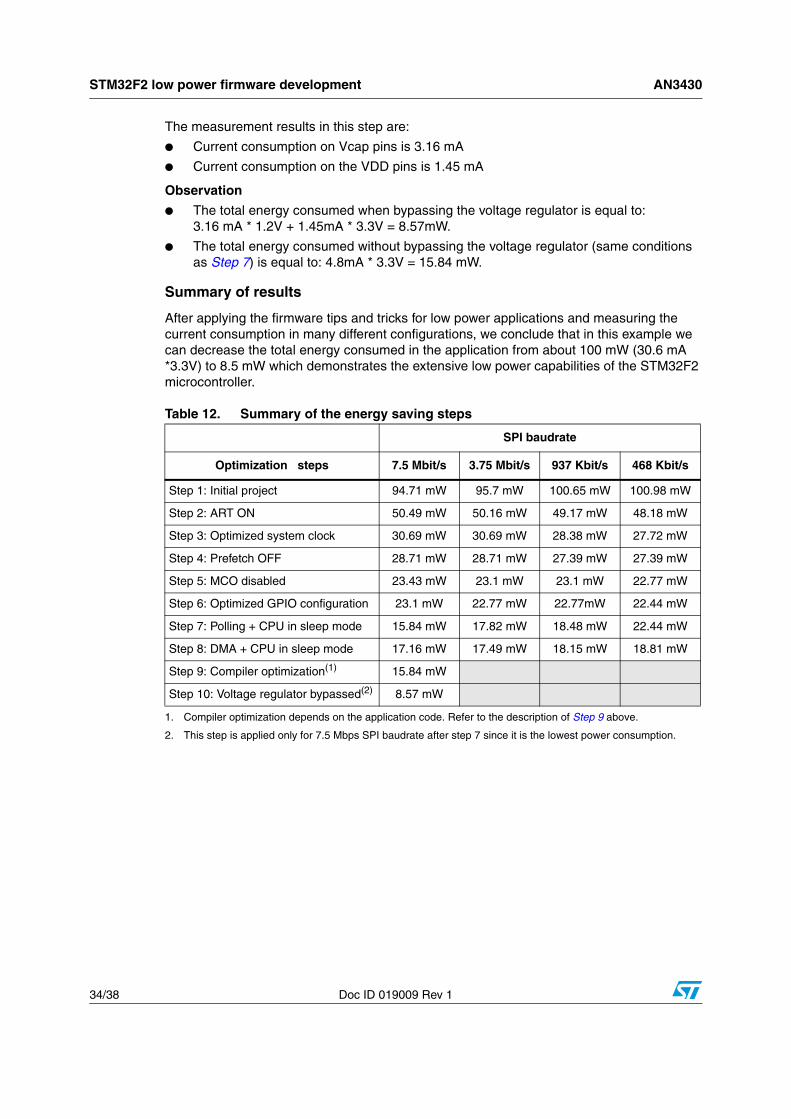
The measurement results in this step are:
● Current consumption on Vcap pins is 3.16 mA
● Current consumption on the VDD pins is 1.45 mA
Observation
● The total energy consumed when bypassing the voltage regulator is equal to: 3.16 mA * 1.2V + 1.45mA * 3.3V = 8.57mW.
● The total energy consumed without bypassing the voltage regulator (same conditions as Step 7) is equal to: 4.8mA * 3.3V = 15.84 mW.
Summary of results
After applying the firmware tips and tricks for low power applications and measuring the current consumption in many different configurations, we conclude that in this example we can decrease the total energy consumed in the application from about 100 mW (30.6 mA *3.3V) to 8.5 mW which demonstrates the extensive low power capabilities of the STM32F2 microcontroller.
Table 12. Summary of the energy saving steps
SPI baudrate
Optimization steps 7.5 Mbit/s 3.75 Mbit/s 937 Kbit/s 468 Kbit/s
Step 1: Initial project 94.71 mW 95.7 mW 100.65 mW 100.98 mW
Step 2: ART ON 50.49 mW 50.16 mW 49.17 mW 48.18 mW
Step 3: Optimized system clock 30.69 mW 30.69 mW 28.38 mW 27.72 mW
Step 4: Prefetch OFF 28.71 mW 28.71 mW 27.39 mW 27.39 mW
Step 5: MCO disabled 23.43 mW 23.1 mW 23.1 mW 22.77 mW
Step 6: Optimized GPIO configuration 23.1 mW 22.77 mW 22.77mW 22.44 mW
Step 7: Polling + CPU in sleep mode 15.84 mW 17.82 mW 18.48 mW 22.44 mW
Step 8: DMA + CPU in sleep mode 17.16 mW 17.49 mW 18.15 mW 18.81 mW
Step 9: Compiler optimization(1)
1. Compiler optimization depends on the application code. Refer to the description of Step 9 above.
15.84 mW
Step 10: Voltage regulator bypassed(2)
2. This step is applied only for 7.5 Mbps SPI baudrate after step 7 since it is the lowest power consumption.
8.57 mW

AN3430 Conclusion
Doc ID 019009 Rev 1 35/38
4 Conclusion
This application note covers hardware and software parameters which influence on the current consumption of the application.
In Section 1, we have presented a theoretical explanation highlighting the parameters which impact the current consumption of any microcontroller-based application. Section 2, then described the low power design of STM32F2 from a hardware point of view, and Section 3 has shown how to optimize a real microcontroller application in terms of current consumption, in this section, an SPI application running on the STM32F2 consuming 95 mW is optimized step-by-step to lower the total consumed energy to only 8.5 mW.
In applications based on the STM32F2xx family that require low power current consumption, developers should methodically apply all these hardware and software tips and tricks to get the lowest possible current consumption in their specific design project.
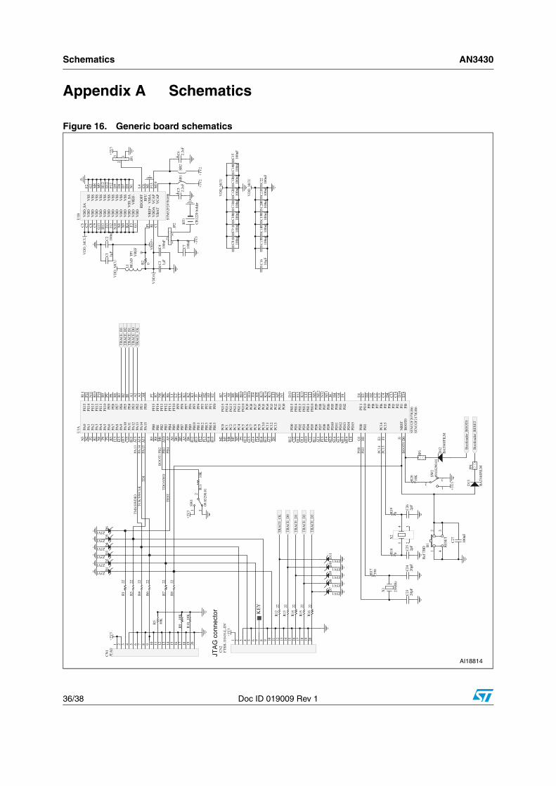
Schematics AN3430
36/38 Doc ID 019009 Rev 1
Appendix A Schematics
Figure 16. Generic board schematics
1 432
B1 RESE
T
C27
100n
F
C24
20pF
C23
20pFX
1
25M
Hz
R17
390
R20
10K
+3V
323
1
SW2
09.0
3290
.01
41
32
X2
Ref T
BD
C26
2pF
C25
2pF
R19
0R1
80
Boot
load
er_B
OO
T0
Boot
load
er_R
ESET
PC14
PC15
PH0
PH1
BT1
CR1
220
hold
er
L1 BEA
D
C4 100n
F
R2 0V
DD
A
VD
D_M
CU
VRE
F+C2 100n
F
TP1
VRE
F
12
3
JP2
+3V
3
VD
D_M
CU
C20
100n
F
VD
D_M
CU
C5 2.2u
FC6 2.
2uF
C21
100n
FC
2210
0nF
C7 100n
F
C19
100n
FC1
810
0nF
C17
100n
F
C11
100n
F
VD
D_M
CU
C12
100n
FC
1310
0nF
C14
100n
FC1
510
0nF
C10
100n
FC9 10
0nF
C8 100n
F
+3V
3
BOO
T0
D12
BAT6
0JFI
LM
JP3
D13
BAT6
0JFI
LM
+1V
2+1
V2
JP4
SB1
SB2
PE2
A2
PE3
A1
PE4
B1PE
5B2
PE6
B3
PI8
D2
PC13
D1
PC14
E1
PC15
F1
PI9
D3
PI10
E3PI
11E4
PF0
E2PF
1H
3PF
2H
2PF
3J2
PF4
J3PF
5K
3PF
6K
2PF
7K
1PF
8L3
PF9
L2PF
10L1
PH0
G1
PH1
H1
NRS
TJ1
PC0
M2
PC1
M3
PC2
M4
PC3
M5
PA0
N3
PA1
N2
PA2
P2
PH2
F4PH
3G
4PH
4H
4PH
5J4
PA3
R2
PA4
N4
PA5
P4
PA6
P3
PA7
R3
PC4
N5
PC5
P5
PB0
R5
PB1
R4
PB2
M6
PF11
R6PF
12P6
PF13
N6
PF14
R7PF
15P7
PG0
N7
PG1
M7
PE7
R8PE
8P8
PE9
P9PE
10R9
PE11
P10
PE12
R10
PE13
N11
PE14
P11
PE15
R11
PB10
R12
PB11
R13
PH6
M11
PH7
N12
PH8
M12
PH9
M13
PH10
L13
PH11
L12
PH12
K12
PB12
P12
PB13
P13
PB14
R14
PB15
R15
PD8
P15
PD9
P14
PD10
N15
PD11
N14
PD12
N13
PD13
M15
PD14
M14
PD15
L14
PG2
L15
PG3
K15
PG4
K14
PG5
K13
PG6
J15
PG7
J14
PG8
H14
PC6
H15
PC7
G15
PC8
G14
PC9
F14
PA8
F15
PA9
E15
PA10
D15
PA11
C15
PA12
B15
PA13
A15
PH13
E12
PH14
E13
PH15
D13
PI0
E14
PI1
D14
PI2
C14
PI3
C13
PA14
A14
PA15
A13
PC10
B14
PC11
B13
PC12
A12
PD0
B12
PD1
C12
PD2
D12
PD3
D11
PD4
D10
PD5
C11
PD6
B11
PD7
A11
PG9
C10
PG10
B10
PG11
B9PG
12B8
PG13
A8
PG14
A7
PG15
B7
PB3
A10
PB4
A9
PB5
A6
PB6
B6
PB7
B5
BOO
T0D
6
PB8
A5
PB9
B4
PE0
A4
PE1
A3
PI4
D4
PI5
C4PI
6C3
PI7
C2
U1A
STM
32F2
07IG
H6
STM
32F2
17IG
H6
R11
10K
+3V
3
231
SW1
09.0
3290
.01
PA14
PA15
PB2
PB3
PB4
PA13
BOO
T1
1 2 3 4 5 6 7 8 9 10 11 12 13 14 15 16 17 18 19 20
CN1
JTA
G+3
V3
R910
K
R10
10K
R5 10K
JTA
G c
onne
ctor
D1
Z5V1
D6
Z5V1
D5
Z5V1
D4
Z5V1
D3
Z5V1
D2
Z5V1
TMS/
SWD
IOTC
K/S
WCL
KTD
I
TDO
/SW
OTR
ST
C16
10μF
C3 1μF
C1 1μF
VBA
TC1
VSS
F2
VD
DF3
VSS
G2
VD
DG
3V
REF-
N1
VSS
AM
1V
REF+
P1
VD
DA
R1
REG
OFF
L4
VD
DK
4
VSS
M8
VD
DN
8
VSS
M9
VD
DN
9
VCA
PM
10
VD
DN
10
VSS
H12
VD
DJ1
2
VSS
_SA
D5
VD
DJ1
3V
SSG
12V
DD
H13
VCA
PF1
3
VSS
F12
VD
DG
13
VSS
D9
VD
DC9
VSS
D8
VD
DC8
VSS
D7
VD
DC7
RFU
C6
VD
D_S
AC5
U1B
STM
32F2
07IG
H6
12
3
JP1
1 2 3 4 5 6 7 8 9 10 11 12 13 14 15 16 17 18 19 20
CN2
FTSH
-110
-01-
L-D
V+3
V3
KEY
TRA
CE_D
3
TRA
CE_D
2
TRA
CE_D
1
TRA
CE_D
0
TRA
CE_C
K
TRA
CE_D
3TR
ACE
_D2
TRA
CE_D
1TR
ACE
_D0
TRA
CE_C
K
D11
Z5V1
D7
Z5V1
D8
Z5V1
D9
Z5V1
D10
Z5V1
R16
22
R15
22
R14
22
R13
22
R12
22
R822
R722
R622
R422
R322
R122

AN3430 Revision history
Doc ID 019009 Rev 1 37/38
Revision history
Table 13. Document revision history
Date Revision Changes
18-Aug-2011 1 Initial release.

AN3430
38/38 Doc ID 019009 Rev 1
Please Read Carefully:
Information in this document is provided solely in connection with ST products. STMicroelectronics NV and its subsidiaries (“ST”) reserve theright to make changes, corrections, modifications or improvements, to this document, and the products and services described herein at anytime, without notice.
All ST products are sold pursuant to ST’s terms and conditions of sale.
Purchasers are solely responsible for the choice, selection and use of the ST products and services described herein, and ST assumes noliability whatsoever relating to the choice, selection or use of the ST products and services described herein.
No license, express or implied, by estoppel or otherwise, to any intellectual property rights is granted under this document. If any part of thisdocument refers to any third party products or services it shall not be deemed a license grant by ST for the use of such third party productsor services, or any intellectual property contained therein or considered as a warranty covering the use in any manner whatsoever of suchthird party products or services or any intellectual property contained therein.
UNLESS OTHERWISE SET FORTH IN ST’S TERMS AND CONDITIONS OF SALE ST DISCLAIMS ANY EXPRESS OR IMPLIEDWARRANTY WITH RESPECT TO THE USE AND/OR SALE OF ST PRODUCTS INCLUDING WITHOUT LIMITATION IMPLIEDWARRANTIES OF MERCHANTABILITY, FITNESS FOR A PARTICULAR PURPOSE (AND THEIR EQUIVALENTS UNDER THE LAWSOF ANY JURISDICTION), OR INFRINGEMENT OF ANY PATENT, COPYRIGHT OR OTHER INTELLECTUAL PROPERTY RIGHT.
UNLESS EXPRESSLY APPROVED IN WRITING BY TWO AUTHORIZED ST REPRESENTATIVES, ST PRODUCTS ARE NOTRECOMMENDED, AUTHORIZED OR WARRANTED FOR USE IN MILITARY, AIR CRAFT, SPACE, LIFE SAVING, OR LIFE SUSTAININGAPPLICATIONS, NOR IN PRODUCTS OR SYSTEMS WHERE FAILURE OR MALFUNCTION MAY RESULT IN PERSONAL INJURY,DEATH, OR SEVERE PROPERTY OR ENVIRONMENTAL DAMAGE. ST PRODUCTS WHICH ARE NOT SPECIFIED AS "AUTOMOTIVEGRADE" MAY ONLY BE USED IN AUTOMOTIVE APPLICATIONS AT USER’S OWN RISK.
Resale of ST products with provisions different from the statements and/or technical features set forth in this document shall immediately voidany warranty granted by ST for the ST product or service described herein and shall not create or extend in any manner whatsoever, anyliability of ST.
ST and the ST logo are trademarks or registered trademarks of ST in various countries.
Information in this document supersedes and replaces all information previously supplied.
The ST logo is a registered trademark of STMicroelectronics. All other names are the property of their respective owners.
© 2011 STMicroelectronics - All rights reserved
STMicroelectronics group of companies
Australia - Belgium - Brazil - Canada - China - Czech Republic - Finland - France - Germany - Hong Kong - India - Israel - Italy - Japan - Malaysia - Malta - Morocco - Philippines - Singapore - Spain - Sweden - Switzerland - United Kingdom - United States of America
www.st.com