introduction to cmos breathes new life into bit-slice
TRANSCRIPT

Application note
Introduction to CMOS breathes new life into bit-slice
For several years speed/power performance advances in the bipolar bit-slice world have slowed to a crawl. Michael J Miller outlines the potential of high-speed CMOS devices
A few years ago bit-slice components offered designers of high-performance digital systems the most cost-effective way of implementing their systems. The introduction of ASICs, RISC processors and general purpose DSP chips has rather eclipsed bit-slice components. However, bit-slice technology has not stood still. Companies like IDT have enhanced bit-slice components by pro- ducing fast CMOS versions. This application note looks at some of the develop- rnents in this field and describes a bit-slice graphics accelerator.
bit slice CMOS microprocessor architectures
Today's high-performance systems are composed of multiple processors and controllers working together. Several decades ago, in all but the most sophisticated designs, there was one processor doing everything. Now, the descendants of these systems are more like multi-cell organisms where each cell is interacting with other cells and performing a specialized task. For example, a workstation today is composed of a central processor (80286), a graphic/video controller, a communications controller for ETHERNET or token ring, a mathe- matics accelerator and a disc controller (Figure I). Except for the main CPU, all of the other elements are dedicated controllers. When performance counts, microprogram designs today can provide controller solutions that operate at more than 15 MIPS, which is an order of magnitude over what a fixed instruction set processor can pro- vide.
The requirement for many of today's system designs to provide the highest performance possible means there is a requirement for high- performance solutions such as micro- program architectures. The perfor-
Integrated Device Technology Europe Ltd, 21 The Crescent, Leatherhead, Surrey KT22 8DY, UK
mance benefit, however, must always be traded off with the cost in terms of power consumed and number of parts in the design solution. The power and parts count for a solution provided by a given family of devices is directly related to the speed/power ratio of the tech- nology used. For several years the speed/power performance advances in the bipolar bit-slice world have
q
MAIN CPU
O 0
ACCELERATOR
[ FLOATPOINT I PROCESSOR
IOUAL POre RAM I
°l GRAPHICS
CONTROLLER SYSTEM MEMORY
slowed to a mere crawl while other families have moved ahead. The new wave of very high-speed CMOS has entered the bit-slice world, thereby offering ever faster and denser functions.
At the current level of technology, the number of gates, or the speed at which the gates can run in bipolar ICs is limited by the heat dissipation capabilities of the package. If the speed/power product is lowered, more speed can be gained from the same number of gates in the package or more gates can be packaged inside the device at the same speed. Because high-speed CMOS has a speed/power product almost an order of magnitude better than bipolar TTL-ECL, it is becoming the technology of choice for new bit- slice functions today. Many more gates, running at higher speeds than
COMMUNICATIONS CONTROLLER
O
DISK CONTROLLER
Figure 1. Workstation with floating-point math accelerator
0141-9331/91/050279-05 © 1991 Butterworth-Heinemann Ltd
Vol 15 No 5 June 1991 279

Application note the conventional bipolar tech- nologies, may be contained in in- expensive packages. This provides more freedom for new architectures running at higher performance levels. Therefore, very high speed CMOS is here just in time to breathe new life into bit-slice ICs.
COMPARISON OF MICRO- PROCESSOR ARCHITECTURES
In order to understand why micro- programming is still a very important architecture for today's designer, one must compare the fixed instruction set (8086, 68000) versus bit-slice microprocessor architectures. These two different approaches have their major strengths in different areas. The fixed instruction set processors have mainly filled the niche of lower parts count solutions and general purpose computation. In the controller area they have serviced the low-to- medium performance solutions. On the other hand, the microprogram bit-slice products have been utilized in very high-performance control applications and emulation of specialized computer architectures. To see why this is, one must inspect the architectures (shown in Figure 2) more closely.
The fixed instruction set pro-
cessors, like the 68000, fall into a class of machines referred to as the Von Neumann-type architecture which has an address bus and a data bus linking together the processor and the memory. These two buses are sometimes referred to as the Von Neumann bottleneck. This is because all data and program instructions must pass through the address and data bus between the memory and processor. This limits the bandwidth because at any given time, only data or program instruc- tions can be fetched or written. The performance is therefore directly related to the bandwidth of this data path. For example, in a 16MHz 68000 for one memory access, the clock must cycle three times, yielding 5 million datatransfers in one second. To perform any instruction the processor must fetch the op code, source and destination designators, and the data. This can be anywhere from two memory cycles to many memory cycles and averages out around three to five memory cycles. At a bus cycle rate of 5 MHz, this results in approximately 1 to 1.5MIPS, which is a theoretical number that exceeds actual bench- marks for the 68000. Through many years of optimizing the architecture and the instruction set, the fixed instruction microprocessors have become very good at performing
CONTROLLER
68020 & 80386
ADDRESS DATA i MEMORY
(DTA & PROG)
COMPUTATION UNIT
DEDICATED HARDWARE SPECIFIC TO APPLICATION
PERFORMANCE
1.5 MIPS
CONTROLLER
~l-I SEO [ t
I ADDRESS ! PROGRAM MEMORY
DATA t
I INSTRUCTION ] REG i i
Figure 2.
COMPUTATION UNIT
DEDICATED HARDWARE SPECIFIC TO APPLICATION
ADDRESS DATA DATA MEMORY
Comparison of microprocessors as controllers
20 MIPS
general purpose computations. Because the instruction set is fixed and has been added to over the years, software written for these processors has been brought forward, creating a very rich base of application software to solve all sorts of applications such as operating systems, compilers, editors, data base programs etc. Use of high level languages has made this much easier.
The microprogram architecture can be thought of as a Harvard class architecture. This architecture allows instructions to be fetched at the same time that data is fetched, thus over- lapping instruction fetch and decode along with data operations. The heart of the bit-slice architecture is found in the sequencer. The sole purpose of the sequencer is to generate a new address on every clock cycle. These addresses are fed into a programmed memory whose result is stored in an instruction register referred to as the pipeline register. The pipeline register and memory are very w ide - -any - where from 32 bits to as large as 256 bits. The width of this register is tailored in each design in order to control a few or many operations in parallel, tuning the performance to the required application. The instruction register holds the instruction for the sequencer which is generating the next address. With a 20MHz signal clocking the sequencer, a new instruction can be fetched 20 million times per second. This sets an upper end performance level for the bit-slice architecture at 20 MIPS. This very high rate instruc- tion stream can be used as disc controllers, high-speed graphics engines, dedicated DSP architectures for radar/sonar, imaging devices, communications, robotics and so on.
The other half of the Harvard architecture is the portion which processes data (shown in Figure 2) as the computation. This section is typically composed of RAM, arithmetic logic units, multipliers and data conversion elements (for DSP applications). This portion of the architecture can have local memory which is used directly in the computation path, as well as larger more bulky memory. This architecture may be highly pipelined
280 Microprocessors and Microsystems
Application note to get maximum performance or it may be very simple small architec- tures.
The 2900 family is a group of LSI/ VLSI building blocks which provide such functions as sequencers, address generators and data path elements. Typically, devices like the 2910 are used for the sequencer and devices like the 2903 or 2901 are used for the ALUs and the data paths of microprogrammed machines. Because the microprogram devices are thought of more as building blocks, they therefore have the capability and flexibility to emulate many different structures, just as the NAND-gate is the ultimate in flexibility. For example, the 2901 is often used as a sophisticated, dedicated address generator which can perform PC relative operations, calculate pointers into complex data structures etc. Because of the flexi- bility and instruction rate, the micro- program architecture is very suitable for high-performance controllers and the emulation of special purpose computer architectures not available as fixed instruction set machines.
NEW AND MORE POWERFUL BIT-SLICE DEVICES AS A RESULT OF CMOS
Because CMOS consumes an order of magnitude less power for the same speed as bipolar, many more gates may be packed into the same pack- age and still have room to reduce the size of that package. This allows for ever increasing levels of integration. IDT has designed a new family of bit- slice devices which can execute the already-existing microcode of the AMD 2900 family, but at more than four times the integration level. This family is referred to as the IDT49C000 family, and the heart of it is made up of ALUs and sequencers. Two key devices in this family are the IDT49C410 and the IDT49C402. These parts characteristically have wider data paths, more internal paths, larger RAM and support much higher clock rates than their bipolar predecessors.
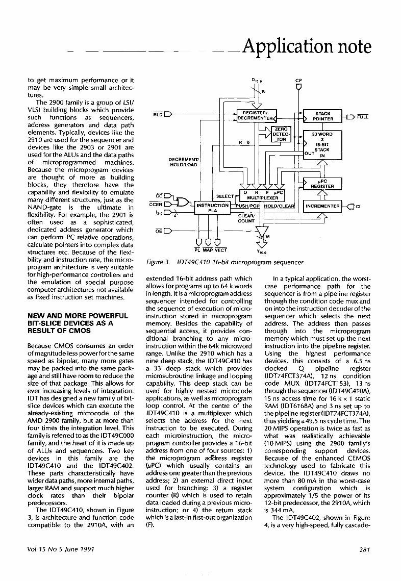
The IDT49C410, shown in Figure 3, is architecture and function code compatible to the 2910A, with an
Dls-o CP
RLD [~>
DECREMEN~ HOLD/LOAD
REGISTER/ STACK " C R E M E N T E R , ~ POINTER ~ [ ~ FULL
R=0
33 WORD X
16-BIT TSTACK
IN
CC ~ _ SELECT
CCEI~ ~ INSTRUCTION ~'- 13-o
OE
D R F ~PC MULTIPLEXER
CLEAR/ COUNT
~PC REGISTER
CI
PL MAP VECT Y15-o
Figure 3. IDT49C410 16-bit microprogram sequencer
extended 16-bit address path which allows for programs up to 64 k words in length. It is a microprogram address sequencer intended for controlling the sequence of execution of micro- instruction stored in microprogram memory. Besides the capability of sequential access, it provides con- ditional branching to any micro- instruction within the 64k microword range. Unlike the 2910 which has a nine deep stack, the IDT49C410 has a 33 deep stack which provides microsubroutine linkage and looping capability. This deep stack can be used for highly nested microcode applications, as well as microprogram loop control. At the centre of the IDT49C410 is a multiplexer which selects the address for the next instruction to be executed. During each microinstruction, the micro- program controller provides a 16-bit address from one of four sources: 1) the microprogram address register (#PC) which usually contains an address one greater than the previous address; 2) an external direct input used for branching; 3) a register counter (R) which is used to retain data loaded during a previous micro- instruction; or 4) the return stack which is a last-in first-out organization (F).
In a typical application, the worst- case performance path for the sequencer is from a pipeline register through the condition code mux and on into the instruction decoder of the sequencer which selects the next address. The address then passes through into the microprogram memory which must set up the next instruction into the pipeline register. Using the highest performance devices, this consists of a 6.5 ns clocked Q pipeline register (IDT74FCT374A), 12 ns condition code MUX (IDT74FCT153), 13ns through the sequencer (IDT49C410A), 15 ns access time for 16 k x 1 static RAM (IDT6168A) and 3 ns set up to the pipeline register (IDT74FCT374A), thusyieldinga49.5 ns cycletime. The 20 MIPS operation is twice as fast as what was realistically achievable (10MIPS) using the 2900 family's corresponding support devices. Because of the enhanced CEMOS technology used to fabricate this device, the IDT49C410 draws no more than 80 mA in the worst-case system configuration which is approximately 1/5 the power of its 12-bit predecessor, the 2910A, which is 344 mA.
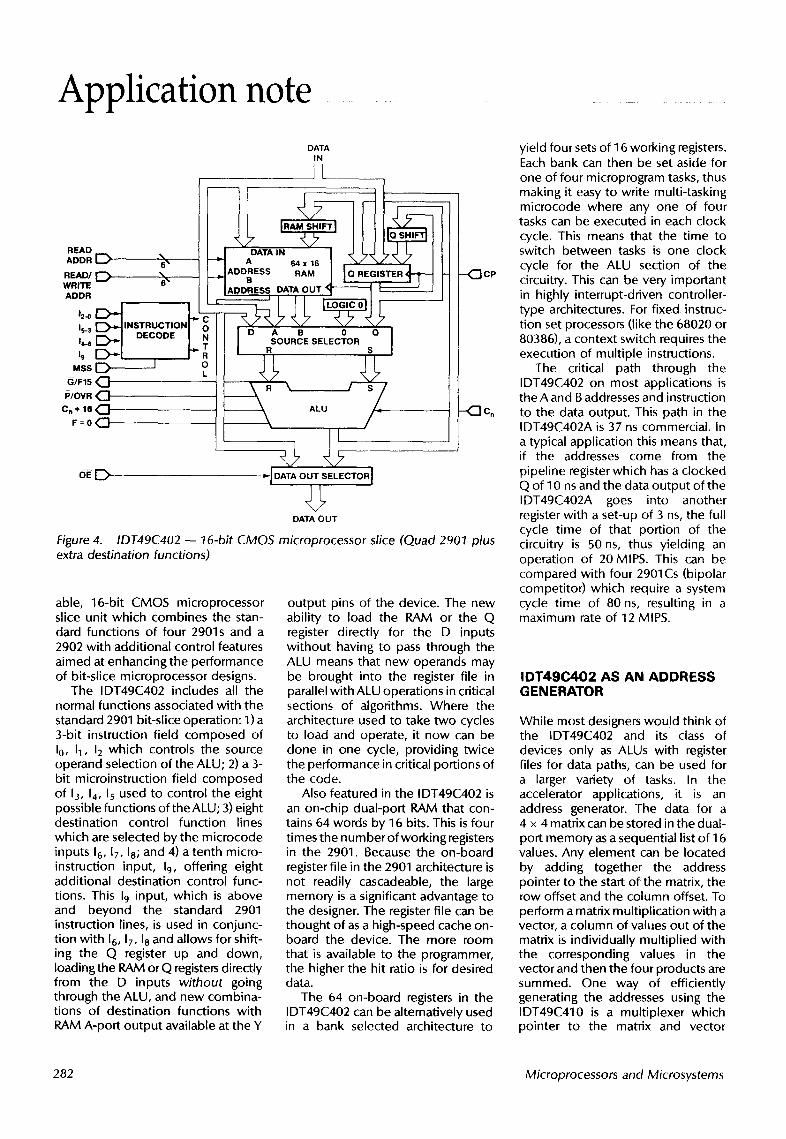
The IDT49C402, shown in Figure 4, is a very high-speed, fully cascade-
Vol 15 No 5 June 1991 281
Application note
READ ADDR
READ/ WRITE ADDR
Is-3 Is-6 19
MSS
G/F15
P/OVR C n + 16
F=0
DECODE
D I o L
G G G CI
DATA IN
Jt
DATA IN A 64x16
ADDRESS RAM B
ADDRESS DATA OUT
D A B 0 Q SOURCE SELECTOR
R S
ALU
- - ~ ] C P
- - C ] Cn
OE D ~-[ DATA OUT SELECTOR]
DATA OUT
Figure 4. IDT49C402 -- 16-bit CMOS microprocessor slice (Quad 2901 plus extra destination functions)
able, 16-bit CMOS microprocessor slice unit which combines the stan- dard functions of four 2901s and a 2902 with additional control features aimed at enhancing the performance of bit-slice microprocessor designs.
The IDT49C402 includes all the normal functions associated with the standard 2901 bit-slice operation: I) a 3-bit instruction field composed of I0, 11, 12 which controls the source operand selection of the ALU; 2) a 3- bit microinstruction field composed of 13, 14, I s used to control the eight possible functions of the ALU; 3) eight destination control function lines which are selected by the microcode inputs 16, 17, 18; and 4) a tenth micro- instruction input, 19, offering eight additional destination control func- tions. This 19 input, which is above and beyond the standard 2901 instruction lines, is used in conjunc- tion with [6, 17, I 8 and allows for shift- ing the Q register up and down, loading the RAM or Q registers directly from the D inputs without going through the ALU, and new combina- tions of destination functions with RAM A-port output available at the Y
output pins of the device. The new ability to load the RAM or the Q register directly for the D inputs without having to pass through the ALU means that new operands may be brought into the register file in parallel with ALU operations in critical sections of algorithms. Where the architecture used to take two cycles to load and operate, it now can be done in one cycle, providing twice the performance in critical portions of the code.
Also featured in the IDT49C402 is an on-chip dual-port RAM that con- tains 64 words by 16 bits. This is four times the number of working registers in the 2901. Because the on-board register file in the 2901 architecture is not readily cascadeable, the large memon I is a significant advantage to the designer. The register file can be thought of as a high-speed cache on- board the device. The more room that is available to the programmer, the higher the hit ratio is for desired data.
The 64 on-board registers in the IDT49C402 can be alternatively used in a bank selected architecture to
yield four sets of 16 working registers. Each bank can then be set aside for one of four microprogram tasks, thus making it easy to write multi-tasking microcode where any one of four tasks can be executed in each clock cycle. This means that the time to switch between tasks is one clock cycle for the ALU section of the circuitry. This can be very important in highly interrupt-driven controller- type architectures. For fixed instruc- tion set processors (like the 68020 or 80386), a context switch requires the execution of multiple instructions.
The critical path through the IDT49C402 on most applications is the A and B addresses and instruction to the data output. This path in the IDT49C402A is 37 ns commercial. In a typical application this means that, if the addresses come from the pipeline register which has a clocked Q of I0 ns and the data output of the IDT49C402A goes into another register with a set-up of 3 ns, the full cycle time of that portion of the circuitry is 50 ns, thus yielding an operation of 20MIPS. This can be compared with four 2901Cs (bipolar competitor) which require a system cycle time of 80ns, resulting in a maximum rate of 12 MIPS.
IDT49C402 AS AN ADDRESS GENERATOR
While most designers would think of the IDT49C402 and its class of devices only as ALUs with register files for data paths, can be used for a larger variety of tasks. In the accelerator applications, it is an address generator. The data for a 4 x 4 matrix can be stored in the dual- port memory as a sequential list of 16 values. Any element can be located by adding together the address pointer to the start of the matrix, the row offset and the column offset. To perform a matrix multiplication with a vector, a column of values out of the matrix is individually multiplied with the corresponding values in the vector and then the four products are summed. One way of efficiently generating the addresses using the IDT49C410 is a multiplexer which pointer to the matrix and vector
282 Microprocessors and Microsystems

Application note stored in the register file. To start, the address pointer of the matrix could be summed with a constant corres- ponding to the column to be operated on. This operation can be accompli- shed in one cycle by bringing the constant in through the 'D' bus from the pipeline register, addressing the pointer with the A address and storing the result at a location specified by the B address. In the same cycle the new address could be output from the ALU through the Y port and placed in the MAR register. In this way, the MAR register would supply the dual-port RAM address on the next cycle, thus forming a pipeline mode of operation. On the next three cycles, the new address stored in the register file could be incremented and the respective calculated addresses passed on to the MAR. Therefore, in four cycles four
addresses can be generated in rapid fire that correspond to four values in the column of the matrix. All of this function can be independent of, and working in parallel with, what is happening in the computation unit. With proper orchestration, addresses can be fed into the dual-port RAM and values read out in succession into the computation unit on every cycle. The minimum time from register file address to the Y output is 37 ns, which is one of the fastest ways to generate complex 16-bit address.
Just as the IDT49C402 can be used to compute offsets into matrices, it can also be used to keep track of linked lists of complex data struc- tures. The register file could be used to retain pointers of various lists, as well as intermediate pointers. In the accelerator described earlier, there are several required pointers: one
pointer to the head of a list of XYZW points, an intermediate pointer to the current XYZW and a pointer to the transformation matrix.
CONCLUSION
The advantage of the MICROSLICE solution is that it can control multiple devices in parallel at the cost of wider control memory and multiple bus interface parts. The speed/power product provided by very high-speed CMOS today offers the designer bit- slice tools for designing control struc- tures and computation units which are on a comparable level of integra- tion with fixed instruction set pro- cessors, but can offer significantly more than an order of magnitude in performance.
Vol 75 No 5 June 7997 283