iraudamp11
TRANSCRIPT

www.irf.com Page 1 of 35 IRAUDAMP11 REV 1.0
IRAUDAMP11
120W x 3 Channel Class D Audio Power Amplifier Using the IRS2053M and IRF6665
By
Jun Honda, Liwei Zheng
CAUTION:
International Rectifier suggests the following guidelines for safe operation and handling of IRAUDAMP11 Demo board;
Always wear safety glasses whenever operating Demo Board Avoid personal contact with exposed metal surfaces when operating Demo Board Turn off Demo Board when placing or removing measurement probes

www.irf.com Page 2 of 35 IRAUDAMP11 REV 1.0
TABLE OF CONTENTS PAGE
INTRODUCTION............................................................................................................................................... 3
SPECIFICATIONS............................................................................................................................................ 3
CONNECTION SETUP..................................................................................................................................... 5
CONNECTOR DESCRIPTION ......................................................................................................................... 5
TEST PROCEDURES....................................................................................................................................... 6
PERFORMANCE AND TEST GRAPHS .......................................................................................................... 7
CLIPPING CHARACTERISTICS.................................................................................................................... 10
SOFT CLIPPING............................................................................................................................................. 10
EFFICIENCY................................................................................................................................................... 12
THERMAL CONSIDERATIONS..................................................................................................................... 12
THERMAL INTERFACE MATERIAL’S PRESSURE CONTROL ................................................................................. 13
POWER SUPPLY REJECTION RATIO (PSRR)............................................................................................ 15
SHORT CIRCUIT PROTECTION RESPONSE .............................................................................................. 16
IRAUDAMP11 OVERVIEW ............................................................................................................................ 17
FUNCTIONAL DESCRIPTIONS..................................................................................................................... 19
IRS2053 GATE DRIVER IC ............................................................................................................................ 19 SELF-OSCILLATING FREQUENCY .................................................................................................................... 20 ADJUSTMENTS OF SELF-OSCILLATING FREQUENCY......................................................................................... 20 SELECTABLE DEAD-TIME................................................................................................................................ 21
PROTECTION SYSTEM OVERVIEW ............................................................................................................ 22
CLICK AND POP NOISE REDUCTION......................................................................................................... 24
BUS PUMPING............................................................................................................................................... 24
INPUT SIGNAL AND GAIN SETTING ........................................................................................................... 26
GAIN SETTING............................................................................................................................................... 26
IRAUDAMP11 FABRICATION MATERIALS................................................................................................. 28
IRAUDAMP11 HARDWARE .......................................................................................................................... 31
IRAUDAMP11 PCB SPECIFICATIONS......................................................................................................... 32
REVISION CHANGES DESCRIPTIONS........................................................................................................ 35

www.irf.com Page 3 of 35 IRAUDAMP11 REV 1.0
Introduction The IRAUDAMP11 Demo board is a reference design which uses only one IC (IRS2053M) to derive appropriate input signals, amplify the audio input, and achieve a three-channel 120 W/ch (4Ω, THD+N=1%) half-bridge Class D audio power amplifier. The reference design demonstrates how to use the IRS2053M Class D audio controller and gate driver IC, implement protection circuits, and design an optimum PCB layout using IRF6665 DirectFET MOSFETs. The reference design contains all the required housekeeping power supplies for ease of use. The three-channel design is scalable, for power and number of channels.
Applications
AV receivers Home theater systems Mini component stereos Powered speakers Sub-woofers Musical Instrument amplifiers Automotive after market amplifiers
Features
Output Power: 120W x 3 channels (4Ω, THD+N=1%)
or 170W x 3 channels (4Ω, THD+N=10%) Residual Noise: 220V, IHF-A weighted, AES-17 filter Distortion: 0.02% THD+N @ 60W, 4Ω Efficiency: 90% @ 120W, 4Ω, single-channel driven, Class D stage Multiple Protection Features: Over-current protection (OCP), high side and low side
Over-voltage protection (OVP), Under-voltage protection (UVP), high side and low side Over-temperature protection (OTP)
PWM Modulator: Self-oscillating half-bridge topology with optional clock synchronization
Specifications
General Test Conditions (unless otherwise noted) Notes / Conditions Supply Voltages ±35V Load Impedance 4Ω Self-Oscillating Frequency 400kHz No input signal, Adjustable Gain Setting 28dB 1Vrms input yields rated power
Electrical Data Typical Notes / Conditions IR Devices Used IRS2053M Audio Controller and Gate-Driver,
IRF6665 DirectFET MOSFETs Modulator Self-oscillating, second order sigma-delta modulation, analog input Power Supply Range ± 25V to ±35V Bipolar power supply Output Power CH1-3: (1% THD+N) 120W 1kHz, ±35V Output Power CH1-3: (10% THD+N) 170W 1kHz, ±35V

www.irf.com Page 4 of 35 IRAUDAMP11 REV 1.0
Rated Load Impedance 8-4Ω Resistive load Standby Supply Current +75/-95mA No input signal Total Idle Power Consumption 6W No input signal Channel Efficiency 90% Single-channel driven,
120W, Class D stage
. Audio Performance Class D
Output Notes / Conditions
THD+N, 1W THD+N, 10W THD+N, 60W THD+N, 100W
0.015% 0.01% 0.02% 0.03%
1kHz, Single-channel driven
Dynamic Range 101dB A-weighted, AES-17 filter, Single-channel operation
Residual Noise, 22Hz - 20kHzAES17 220V
Self-oscillating – 400kHz
Damping Factor 67 1kHz, relative to 4Ω load Channel Separation 75dB
75dB 70dB
100Hz 1kHz 10kHz
Frequency Response : 20Hz-20kHz : 20Hz-35kHz
±1dB ±3dB
1W, 4Ω - 8Ω Load
Physical Specifications Dimensions 3.94”(L) x 2.83”(W) x 0.85”(H)
100 mm (L) x 72 mm (W) x 21.5 mm(H) Weight 0.130kgm

www.irf.com Page 5 of 35 IRAUDAMP11 REV 1.0
Connection Setup
Fig 1 Typical Test Setup
Connector Description
CH1 IN CN1 Analog input for CH1 CH2 IN CN1 Analog input for CH2 CH3 IN CN1 Analog input for CH3 SUPPLY P1 Positive and negative supply (+B / -B) CH1 OUT P2 Output for CH1 CH2 OUT P2 Output for CH2 CH3 OUT P3 Output for CH3
250W, 4Ω, Non-inductive Resistors
Frequency adjustor VCC INDICATOR
IRF6665
CH1 CH2 CH3
IRS2053M
CH2 CH1 +B GND -B CH3Output
Input
G
DS1
35 V, 5 A DC supply
35 V, 5 A DC supply
Audio Signal Generator
Output
VR1

www.irf.com Page 6 of 35 IRAUDAMP11 REV 1.0
Test Procedures Test Setup:
1. Connect 4-200 W dummy loads to 3 output connectors (P2 and P3 as shown on Fig 1) and an Audio Precision analyzer (AP).
2. Connect the Audio Signal Generator to CN1 for CH1~CH3 respectively (AP). 3. Set up the dual power supply with voltages of ±35V; current limit to 5A. 4. TURN OFF the dual power supply before connecting to On of the unit under test (UUT). 5. Connect the dual power supply to P1. as shown on Fig 1
Power up:
6. Turn ON the dual power supply. The ±B supplies must be applied and removed at the
same time. 7. The Blue LED should turn ON immediately and stay ON 8. Quiescent current for the positive supply should be 75mA 10mA at +35V. 9. Quiescent current for the negative supply should be 95mA 10mA at –35V.
Switching Frequency test
10. With an Oscilloscope, monitor the switching waveform at test points VS1~VS3. Adjust VR1 to set the self oscillating frequency to 400 kHz 25 kHz when DUT in clock synchronize mode.
Functionality Audio Tests:
11. Set the signal generator to 1kHz, 20 mVRMS output. 12. Connect the audio signal generator to CN1(Input of CH1,CH2,CH3) 13. Sweep the audio signal voltage from 15 mVRMS to 1 VRMS. 14. Monitor the output signals at P2/P3 with an oscilloscope. The waveform must be a non
distorted sinusoidal signal. 15. Observe that a 1 VRMS input generates an output voltage of 25.52 VRMS(CH1/CH2). The
ratio, R4x/(R3x) and R30x/(R31x), determines the voltage gain of IRAUDAMP11. Test Setup using Audio Precision (Ap):
16. Use an unbalanced-floating signal from the generator outputs. 17. Use balanced inputs taken across output terminals, P2 and P3. 18. Connect Ap frame ground to GND at terminal P1. 19. Select the AES-17 filter(pull-down menu) for all the testing except frequency response. 20. Use a signal voltage sweep range from 15 mVRMS to 1 VRMS. 21. Run Ap test programs for all subsequent tests as shown in Fig 2- Fig 7below.

www.irf.com Page 7 of 35 IRAUDAMP11 REV 1.0
Performance and test graphs
ColorS weep Trace Line S ty le Thick Data A x is Com m ent
1 1 Red S olid 2 A nlr.THD+ N Ratio Left CH11 3 B lue S olid 2 A nlr.THD+ N Ratio Left CH22 3 Green S olid 2 A nlr.THD+ N Ratio Left
0.001
10
0.002
0.005
0.01
0.02
0.05
0.1
0.2
0.5
1
2
5
%
100m 200200m 500m 1 2 5 10 20 50 100
W
±B Supply = ±35V, 4 Ω Resistive Load
Fig 2 IRAUDAMP11, THD+N versus Power, Stereo, 4 Ω
.
-10
+4
-9
-8
-7
-6
-5
-4
-3
-2
-1
-0
+1
+2
+3
dBr A
20 200k50 100 200 500 1k 2k 5k 10k 20k 50k 100k
Hz
T
CH1-Blue; CH2-Yellow; CH3-Red ±B Supply = ±35V, 4 Ω Resistive Load
Fig 3 IRAUDAMP11, Frequency response
www.irf.com Page 8 of 35 IRAUDAMP11 REV 1.0
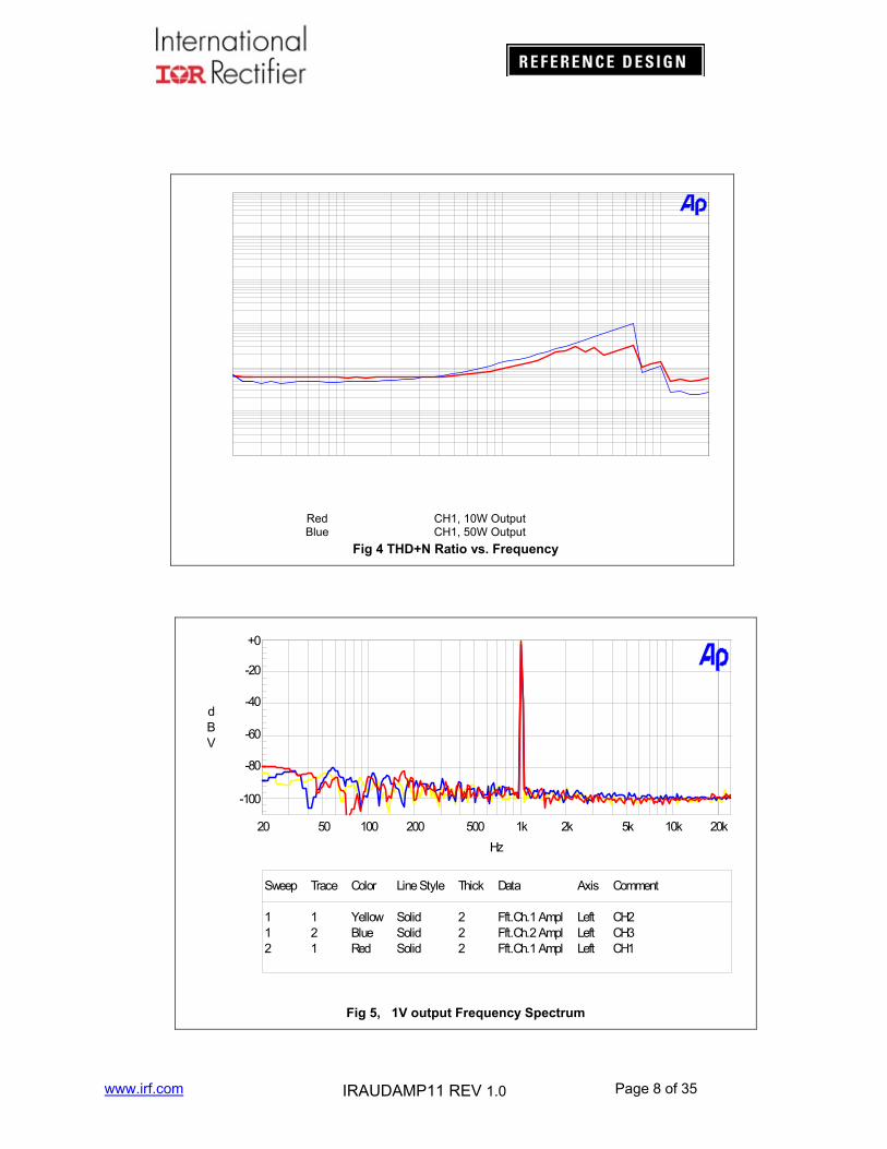
Red CH1, 10W Output Blue CH1, 50W Output
Fig 4 THD+N Ratio vs. Frequency
ColorSweep Trace Line Style Thick Data Axis Comment
1 1 Yellow Solid 2 Fft.Ch.1 Ampl Left CH21 2 Blue Solid 2 Fft.Ch.2 Ampl Left CH32 1 Red Solid 2 Fft.Ch.1 Ampl Left CH1
-100
+0
-80
-60
-40
-20
dBV
20 20k50 100 200 500 1k 2k 5k 10k
Hz
Fig 5, 1V output Frequency Spectrum

www.irf.com Page 9 of 35 IRAUDAMP11 REV 1.0
ColorSweep Trace Line Style Thick Data Axis Comment
1 1 Red Solid 2 Fft.Ch.1 Ampl Left CH11 2 Blue Solid 2 Fft.Ch.2 Ampl Left CH32 1 Yellow Solid 2 Fft.Ch.1 Ampl Left CH2
-150
+0
-125
-100
-75
-50
-25
dBV
10 20k20 50 100 200 500 1k 2k 5k 10k
Hz
No signal, Self Oscillator @ 400kHz Fig 6, IRAUDAMP11 Noise Floor
.
ColorS weep Trac e Line S ty le Thic k Data A x is Com m ent
1 1 Cy an S olid 2 A nlr.A m pl Left CH3_on;CH1_off3 1 Y ellow S olid 2 A nlr.A m pl Left CH1_on;CH3_off4 1 Red S olid 2 A nlr.A m pl Left CH2_on;CH3_off5 1 M agenta S olid 2 A nlr.A m pl Left CH3_on;CH2_off6 1 B lue S olid 1 A nlr.A m pl Left CH2_on;CH1_off7 1 Cy an S olid 1 A nlr.A m pl Left Ch1_on;CH2_off
-100
+ 0
-90
-80
-70
-60
-50
-40
-30
-20
-10
dBr
A
20 20k50 100 200 500 1k 2k 5k 10k
Hz
Fig 7, Channel separation vs. frequency
www.irf.com Page 10 of 35 IRAUDAMP11 REV 1.0
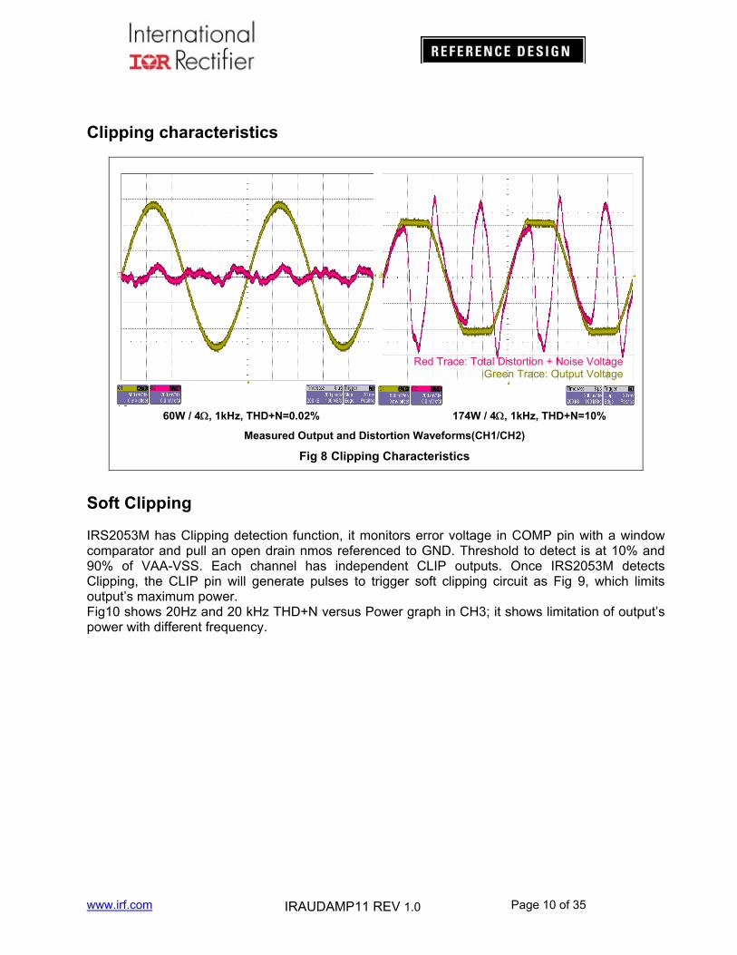
Clipping characteristics
60W / 4, 1kHz, THD+N=0.02% 174W / 4, 1kHz, THD+N=10%
Measured Output and Distortion Waveforms(CH1/CH2)
Fig 8 Clipping Characteristics
.
Soft Clipping IRS2053M has Clipping detection function, it monitors error voltage in COMP pin with a window comparator and pull an open drain nmos referenced to GND. Threshold to detect is at 10% and 90% of VAA-VSS. Each channel has independent CLIP outputs. Once IRS2053M detects Clipping, the CLIP pin will generate pulses to trigger soft clipping circuit as Fig 9, which limits output’s maximum power. Fig10 shows 20Hz and 20 kHz THD+N versus Power graph in CH3; it shows limitation of output’s power with different frequency.
Red Trace: Total Distortion + Noise Voltage Green Trace: Output Voltage

www.irf.com Page 11 of 35 IRAUDAMP11 REV 1.0
R3A 1K
GND
C5A10uF, 50V
Audio signal INPUT
S
G
D
Q6MMBFJ112
R28A1K
R29A220K
D3A1N4148
C15A10uF, 16V
Q5DTA144EKA
R27A
3.3K
R5A47K
R6A47K
C6A1uF,50V
R7A470K
10uF,50V
C0A
Soft Clipping
CLIP Detection
IN-
VSS
GND
VAA
Fig 9 Soft Clipping Circuit
ColorSweep Trace Line Style Thick Data Axis Comment
1 1 Red Solid 2 Anlr.THD+N Ratio Left 20Hz2 1 Blue Solid 2 Anlr.THD+N Ratio Left 20kHz
0.001
10
0.002
0.005
0.01
0.02
0.05
0.1
0.2
0.5
1
2
5
%
100m 300200m 500m 1 2 5 10 20 50 100
W
±B Supply = ±35V, 4 Ω Resistive Load
Fig 10 IRAUDAMP11/CH3, THD+N versus Power, Stereo, 4 Ω

www.irf.com Page 12 of 35 IRAUDAMP11 REV 1.0
Efficiency Fig 11 shows efficiency characteristics of the IRAUDAMP11. The high efficiency is achieved by following major factors:
1) Low conduction loss due to the DirectFETs offering low RDS(ON)
2) Low switching loss due to the DirectFETs offering low input capacitance for fast rise and fall times
Secure dead-time provided by the IRS2053M, avoiding cross-conduction.
0%
10%
20%
30%
40%
50%
60%
70%
80%
90%
100%
0 50 100 150
Output power (W)
Eff
icie
ncy
(%
)
AMP11 35V 4ohms
Fig 11, IRAUDAMP11 4 ohms load Stereo, ±B supply = ±35V
Thermal Considerations
With this high efficiency, the IRAUDAMP11 design can handle one-eighth of the continuous rated power, which is generally considered to be a normal operating condition for safety standards, without additional heatsinks or forced air-cooling.
Efficiency (%)

www.irf.com Page 13 of 35 IRAUDAMP11 REV 1.0
Thermal Interface Material’s Pressure Control The pressure between DirectFET & TIM (Thermal Interface Material) is controlled by depth of Heat Spreader’s groove. Choose TIM which is recommended by IR. (Refer to AN-1035 for more details). TIM’s manufacturer thickness, conductivity, & etc. determine pressure requirement. Below shows selection options recommended:
Fig 12 TIM Information
www.irf.com Page 14 of 35 IRAUDAMP11 REV 1.0
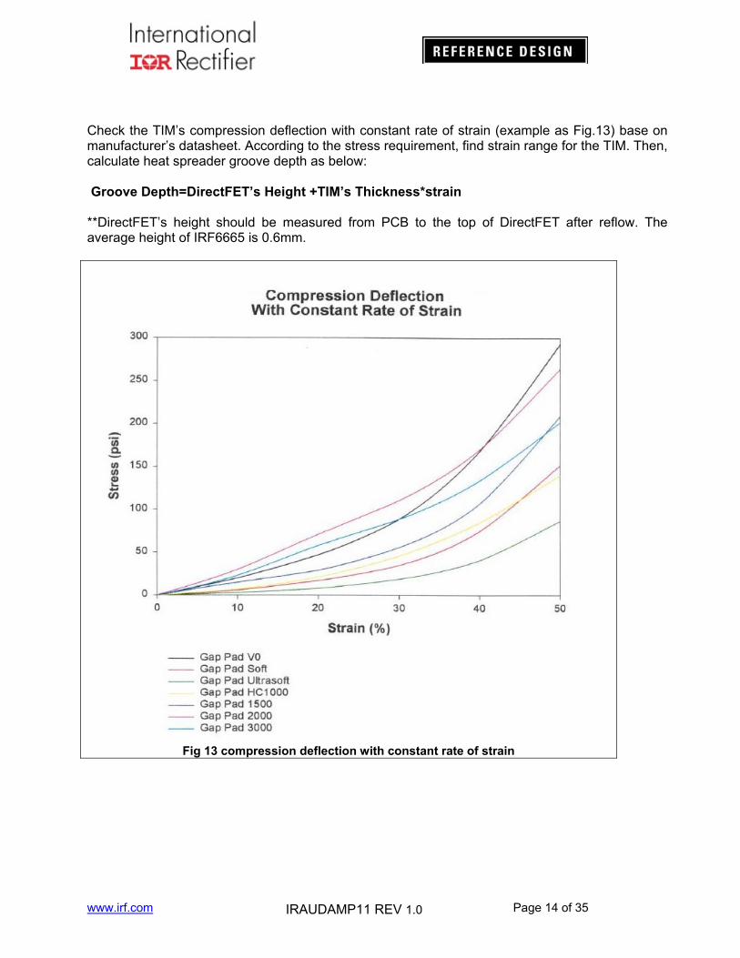
Check the TIM’s compression deflection with constant rate of strain (example as Fig.13) base on manufacturer’s datasheet. According to the stress requirement, find strain range for the TIM. Then, calculate heat spreader groove depth as below: Groove Depth=DirectFET’s Height +TIM’s Thickness*strain **DirectFET’s height should be measured from PCB to the top of DirectFET after reflow. The average height of IRF6665 is 0.6mm.
Fig 13 compression deflection with constant rate of strain

www.irf.com Page 15 of 35 IRAUDAMP11 REV 1.0
Power Supply Rejection Ratio (PSRR) The IRAUDAMP11 obtains good power supply rejection ratio of -68 dB at 1kHz shown in Fig 14. With this high PSRR, IRAUDAMP11 accepts any power supply topology when the supply voltages fit between the min and max range.
ColorSweep Trace Line Style Thick Data Axis Comment
1 1 Magenta Solid 2 Anlr.Ampl Left
-90
+0
-80
-70
-60
-50
-40
-30
-20
-10
dBV
20 40k50 100 200 500 1k 2k 5k 10k 20k
Hz
Fig 14 Power Supply Rejection Ratio (PSRR)
www.irf.com Page 16 of 35 IRAUDAMP11 REV 1.0
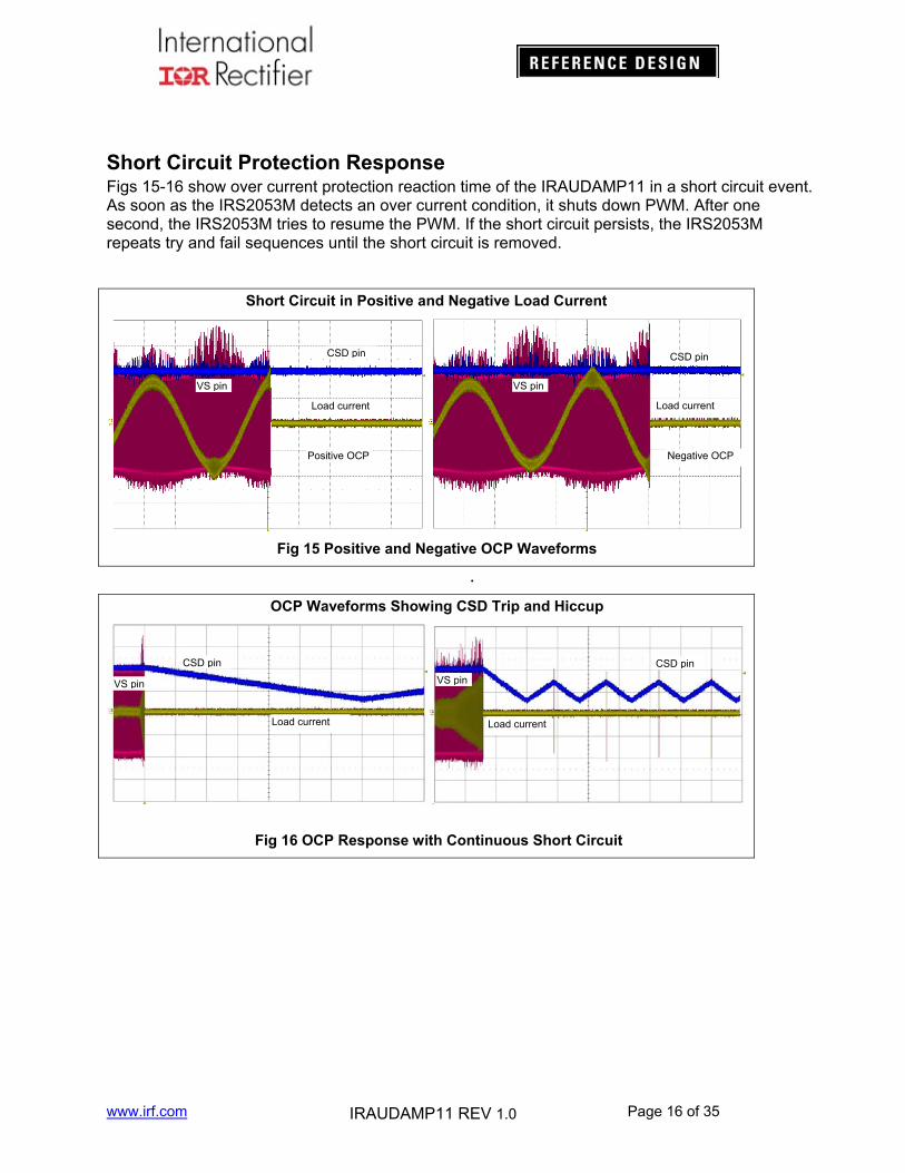
Short Circuit Protection Response Figs 15-16 show over current protection reaction time of the IRAUDAMP11 in a short circuit event. As soon as the IRS2053M detects an over current condition, it shuts down PWM. After one second, the IRS2053M tries to resume the PWM. If the short circuit persists, the IRS2053M repeats try and fail sequences until the short circuit is removed.
Short Circuit in Positive and Negative Load Current
Fig 15 Positive and Negative OCP Waveforms
.
OCP Waveforms Showing CSD Trip and Hiccup
Fig 16 OCP Response with Continuous Short Circuit
Load current
CSD pin
VS pin
Load current
CSD pin
VS pin
Load current
CSD pin
Load current
VS pin
CSD pin
VS pin
Load current
VS pin
Load current
VS pin
Positive OCP Negative OCP

www.irf.com Page 17 of 35 IRAUDAMP11 REV 1.0
IRAUDAMP11 Overview
The IRAUDAMP11 features a 3CH self-oscillating type PWM modulator for the smallest space, highest performance and robust design. This topology represents an analog version of a second-order sigma-delta modulation having a Class D switching stage inside the loop. The benefit of the sigma-delta modulation, in comparison to the carrier-signal based modulation, is that all the error in the audible frequency range is shifted to the inaudible upper-frequency range by nature of its operation. Also, sigma-delta modulation allows a designer to apply a sufficient amount of error correction. The IRAUDAMP11 self-oscillating topology consists of following essential functional blocks.
Front-end integrator PWM comparator Level shifters Gate drivers and MOSFETs Output LPF
Integrator Referring to Fig 17 below, the input operational amplifier of the IRS2053M forms a front-end second-order integrator with R3x, C2x, C3x, and R2x. The integrator that receives a rectangular feedback signal from the PWM output via R4x and audio input signal via R3x generates a quadratic carrier signal at the COMP pin. The analog input signal shifts the average value of the quadratic waveform such that the duty cycle varies according to the instantaneous voltage of the analog input signal. PWM Comparator The carrier signal at the COMP pin is converted to a PWM signal by an internal comparator that has a threshold at middle point between VAA and VSS. The comparator has no hysteresis in its input threshold. Level Shifters The internal input level-shifter transfers the PWM signal down to the low-side gate driver section. The gate driver section has another level-shifter that level shifts up the high-side gate signal to the high-side gate driver section.

www.irf.com Page 18 of 35 IRAUDAMP11 REV 1.0
Gate Drivers and DirectFETs The received PWM signal is sent to the dead-time generation block where a programmable amount of dead time is added into the PWM signal between the two gate output signals of LO and HO to prevent potential cross conduction across the output power DirectFETs. The high-side level-shifter shifts up the high-side gate drive signal out of the dead-time block. Each channel of the IRS2053M’s drives two DirectFETs, high- and low-sides, in the power stage providing the amplified PWM waveform. Output LPF The amplified PWM output is reconstructed back to an analog signal by the output LC LPF. Demodulation LC low-pass filter (LPF) formed by L1 and C13, filters out the Class D switching carrier signal leaving the audio output at the speaker load. A single stage output filter can be used with switching frequencies of 400 kHz and greater; a design with a lower switching frequency may require an additional stage of LPF.
Fig 17 Simplified Block Diagram of IRAUDAMP11 Class D Amplifier
www.irf.com Page 19 of 35 IRAUDAMP11 REV 1.0
Functional Descriptions
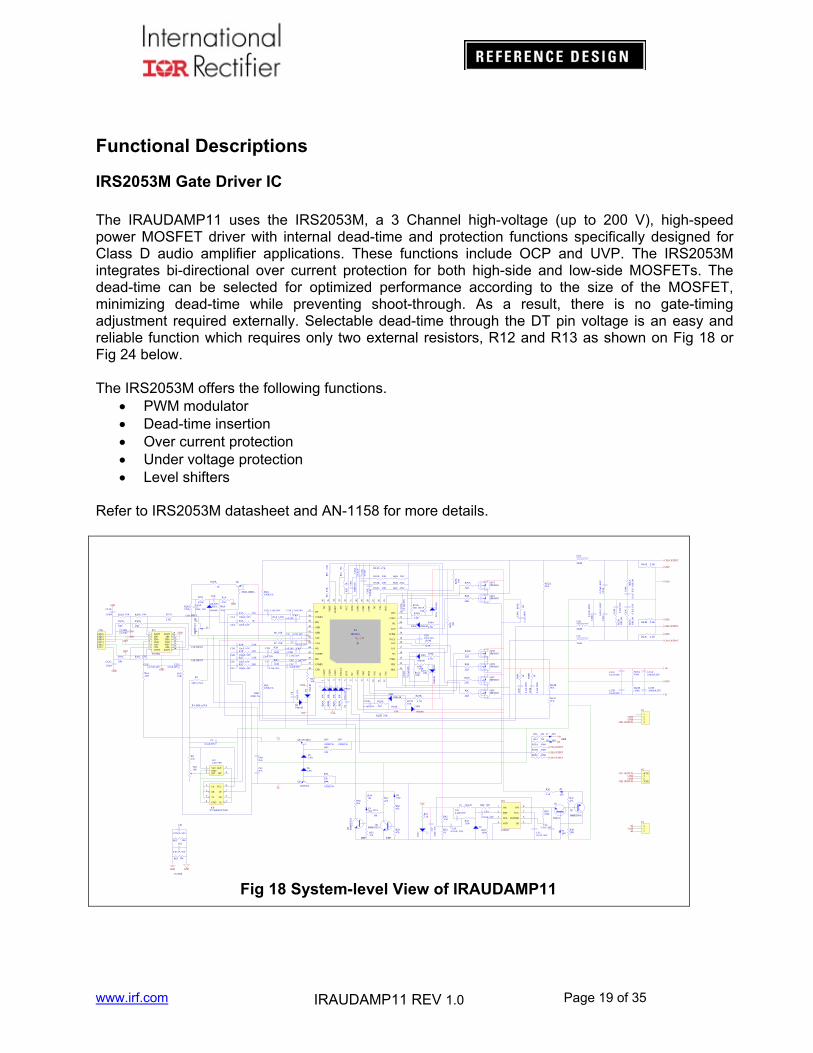
IRS2053M Gate Driver IC The IRAUDAMP11 uses the IRS2053M, a 3 Channel high-voltage (up to 200 V), high-speed power MOSFET driver with internal dead-time and protection functions specifically designed for Class D audio amplifier applications. These functions include OCP and UVP. The IRS2053M integrates bi-directional over current protection for both high-side and low-side MOSFETs. The dead-time can be selected for optimized performance according to the size of the MOSFET, minimizing dead-time while preventing shoot-through. As a result, there is no gate-timing adjustment required externally. Selectable dead-time through the DT pin voltage is an easy and reliable function which requires only two external resistors, R12 and R13 as shown on Fig 18 or Fig 24 below. The IRS2053M offers the following functions.
PWM modulator Dead-time insertion Over current protection Under voltage protection Level shifters
Refer to IRS2053M datasheet and AN-1158 for more details.
C4A1nF,50V
C2A 2.2nF,50V
R2A 120R
C3B
2.2nF,50V
C4B1nF,50V
C2C
2.2nF,50V
R7 10R
C6 4.7uF,10V
C74.7uF,10V
C2B
2.2nF,50V
R6 10R
R20A
22R
R9A
22R
R9B
22R
R9C
22R
R20C
22R
R20B
22R
R21
A10
R,1
W
C13
A0.
47uF
, 400
VC
13C
0.47
uF, 4
00V
C13
B0.47
uF, 4
00V
C14
A
0.1u
F, 6
3V
CH3 OUTPUT
CH2 OUTPUT
CH1 OUTPUT
R15B
10K R16B
3.9K
R17B10K
R15C10K
R16C3.9K
R17C10K
D1C
1N41
48
D1B
1N4148
D2B1N4148
R18B
4.7R
R14B
4.7R
C9B10uF,16V
R16A
3.9K
D1A
1N41
48R15A10K R17A
10K
R14A 4.7R
C9A
10uF
,16V
R13
1K
R12
NC
R11
8.2K
R10
2.2K
R4A100K 1%
R2B
120R
R3B 5.6K
R1B 22K
R2C
120RR1C 22K
R4B100K 1%
R4C100K 1%
C4C 1nF,50V
C3C2.2nF,50V
R3A 1K
R1A 22K
C1A 100pF, 50V
R3C 5.6K
C3A 2.2nF,50V
D2A 1N4148
R18A
4.7R
D2C
1N4148
R18C
4.7R
R21
C10
R,1
W
R21
B10
R,1
W
C14
C
0.1u
F, 6
3V
C14
B
0.1u
F, 6
3V
CL
IP1
3
CL
IP2
2
CL
IP3
1
CSD48
GND41
GND40
DS37
IN339
VAA43
DC
P5
NC
27
OT
P330
NC
36
COMP245
NC16
LO117
CSH3 23
VS3
26
VB
28
OT
P128
VC
C32
COMP147
NC22
VR
EF
35
OC
SET
34
CSH115
LO321
VB3 24
HO
325
COM220
LO2 18
NC
6C
OM
31
HO
29
VS2
10
FAU
LT
4
NC
11
VS1
12
HO113
VB114
OT
P229
DT
33
IN244
IN146
CSH
27
VCC219
COMP338
VSS42
-B0
IC1
IRS2053
C19
A
0.1u
F,10
0V
R19
A
1R
R19
C
1R
C19
B
0.1u
F,10
0V
R19
B
1R
R2210R
D3
1N41
48
R22
C10
K
R22B 10K
Q1AIRF6665
Q2AIRF6665
Q2CIRF6665
Q1BIRF6665
Q2BIRF6665
Q1CIRF6665
C1B 100pF, 50V
C1C 100pF, 50V
GND
GND
GND
GND
CSD
GND
GND
GND
D41N4148
C5A 10uF, 16V
C5B 10uF, 16V
C5C 10uF, 16V
R24A 2.2K
R24C 2.2K
R24B 2.2K
R322k
C1
0.1uF,50V
VR110K
C40N/A
C41N/A
C8
10uF
, 16V
VCC1 OUT 5
SET3GND2
DIT 4
IC2LTC1799
R43
330R,1W
R44
510R,1W
C17B1000uF,35V
C17A1000uF,35V
C17C0.1uF,50V
C17D0.1uF,50V
R23B100k
R23A100k
1A1
1B2
2Y3
GND4
2A5
2B6
1Y7
VCC8
IC8TC7W00FFCT-ND
L5 220uH
C322.2uF, 50V
C37
22uF
, 16V
C330.1uF, 50V
C34
0.01uF, 25V
C352.2nF,50V
C360.01uF, 50V
R39100k
R40100k
R423.3k
R321k
R41120k
D7
R315.1k
DS1
Q1
FX491
Q2
MMBT5401
R3810R
R3747k
Z124V
Z2
15V
R36
5.1k
SW1
BST2
RCL3
RTN4
VIN8
VCC 7
RON/SD 6
FB 5
IC9
LM5007Q3
MM
BT
5551
Q4MMBT5551
R5410k
R5547k
R53
10k
R5747k
R5047k
R5847k
Z339V
Z418V
OVP UVP
+B
GND
-B
R46
33k
CH3 INPUT
CH2 INPUT
CH1 INPUT
1234
P2
1234
P3
123
P1
+BGND
-B
CH2 OUTPUT
CH1 OUTPUT
GNDGND
CH3 OUTPUTGNDGND
-5v
+5v
VCC
C12A
220pF
VSS
VAA-B
R22
A10
K
C19
C
0.1u
F,10
0V
SD
R5647k
CH2
CH1
C12B220pF
C12C
220pF
Q8 ZX5T853
Q9
ZX5T953
R45
33kZ55.6V
Z65.6V
R4 0R0 or N/A
R1
0R0 or N/A
GND GND
C61
0.01uF, 50V
R61 10k
R62 10k
For EMI
C62
0.01uF, 50V
R12AN/A
R12BN/A
R12CN/A
R26
C10
K
DSCDSB
R26
B10
K
PROT
R10
410
K
CH3 OUTPUT
CH2 OUTPUT
CH1 OUTPUT
R25A 100K
R25B 100K
R25C 100K
RpA 95C
123456
CN1
CH1GNDCH2GND
CH3GND
S
G
DQ6
MM
BFJ
112
R28A
1K
R29A220K
D3A
1N4148
1OUT11IN-2 1IN+
3 VDD4 2IN+5 2IN-6 2OUT7
3OUT8
4IN- 13
4OUT 14
3IN-9
4IN+12
3IN+10
GND11
IC3
TLC084
R30A 10KR31A 10K
R31B
10K
R31C
10K
R47
330R,1W
GND
GND
GND
VAA
R51 10k
R52 10k
Z7 39V
Z8 39V
+B
-BOVP
C15A
10uF, 16V
L1A
22uH
L1B
22uH
L1C
22uH
C10
A0.
1uF,
50V
C10B
0.1uF,50V
C10
C
0.1u
F,50
V
Q5
DTA144EKA
C9
100u
F,4V
R27A
3.3K
R1410R
C104.7uF,10V
DSA
R26
A10
K
GND
RpB 95C
RpC 95C
R30C 15K
R1510R
C114.7uF,10V
R30B
15K
GND
C16
B0.
01uF
R32B 10R
C16
C0.
01uF
R32C 10R
C16
A0.
01uF
R32A 10R
R49 10R
GND
R5A
47K
R6A
47K
C6A
1uF,50V
R7A
470K
Fig 18 System-level View of IRAUDAMP11

www.irf.com Page 20 of 35 IRAUDAMP11 REV 1.0
Self-Oscillating Frequency Self-oscillating frequency is determined by the total delay time along the control loop of the system; the propagation delay of the IRS2053M, the DirectFETs switching speed, the time-constant of front-end integrator (R2, R3, R4, C2, C3 ). Variations in +B and –B supply voltages also affect the self-oscillating frequency. The self-oscillating frequency changes with the duty ratio. The frequency is highest at idling. It drops as duty cycle varies away from 50%.
Adjustments of Self-Oscillating Frequency Use R2 to set different self-oscillating frequencies. The PWM switching frequency in this type of self-oscillating switching scheme greatly impacts the audio performance, both in absolute frequency and frequency relative to the other channels. In absolute terms, at higher frequencies, distortion due to switching-time becomes significant, while at lower frequencies, the bandwidth of the amplifier suffers. In relative terms, interference between channels is most significant if the relative frequency difference is within the audible range. Normally, when adjusting the self-oscillating frequency of the different channels, it is suggested to either match the frequencies accurately, or have them separated by at least 25kHz. Under the normal operating condition with no audio input signal, the switching-frequency is set around 400kHz in the IRAUDAMP11.

www.irf.com Page 21 of 35 IRAUDAMP11 REV 1.0
Selectable Dead-time The dead-time of the IRS2053 is set based on the voltage applied to the DT pin. Fig 19 lists the suggested component value for each programmable dead-time between 45 and 105 ns. All the IRAUDAMP11 models use DT1 (45ns) dead-time.
Dead-time Mode R1 R2 DT/SD Voltage DT1 <10k Open Vcc DT2 5.6k 4.7k 0.46 x Vcc
DT3 8.2k 3.3k 0.29 x Vcc
DT4 Open <10k COM
Recommended Resistor Values for Dead Time Selection
Vcc 0.57xVcc 0.36xVcc 0.23xVcc
105nS
85nS
65nS
45nS
VDT
Dead- time
Vcc
COM
DT
>0.5mA
R1
R2
IRS2053M
Fig 19 Dead-time Settings vs. VDT Voltage

www.irf.com Page 22 of 35 IRAUDAMP11 REV 1.0
Protection System Overview The IRS2053M integrates over current protection (OCP) inside the IC. The rest of the protections, such as over-voltage protection (OVP), under-voltage protection (UVP), and over temperature protection (OTP), are detected externally to the IRS2053M (Fig 20). The external shutdown circuit will disable the output by pulling down CSD pins, (Fig 21). If the fault condition persists, the protection circuit stays in shutdown until the fault is removed.
HT 1OS5
VT 3GND 2
VCC4
IC6LM26CIM5-XHAR51
22k
D514.7V
R52
15k
Q5MMBT5551
R5922k
Q3
MM
BT
5551
Q4MMBT5551
R5410k
R5547k
R53
10k
R5747k
R5047k
R5847k
Z339V
Z418V
OVP UVP
SD
R5647k
R6015k
GND
OTP
-B Fig 20 DCP, OTP, UVP and OVP Protection Circuits
.
Fig 21 Simplified Functional Diagram of OCP
www.irf.com Page 23 of 35 IRAUDAMP11 REV 1.0
Over-Current Protection (OCP) Low-Side Current Sensing
The low-side current sensing feature protects the low side DirectFET from an overload condition from negative load current by measuring drain-to-source voltage across RDS(ON) during its on state. OCP shuts down the switching operation if the drain-to-source voltage exceeds a preset trip level.
The voltage setting on the OCSET pin programs the threshold for low-side over-current sensing. When the VS voltage becomes higher than the OCSET voltage during low-side conduction, the IRS2053 turns the outputs off and pulls CSD down to -VSS.
High-Side Current Sensing
The high-side current sensing protects the high side DirectFET from an overload condition from positive load current by measuring drain-to-source voltage across RDS(ON) during its on state. OCP shuts down the switching operation if the drain-to-source voltage exceeds a preset trip level. High-side over-current sensing monitors drain-to-source voltage of the high-side DirectFET during the on state through the CSH and VS pins. The CSH pin detects the drain voltage with reference to the VS pin, which is the source of the high-side DirectFET. In contrast to the low-side current sensing, the threshold of the CSH pin to trigger OC protection is internally fixed at 1.2V. An external resistive divider R15, R16 and R17 are used to program a threshold as shown in Fig 20. An external reverse blocking diode D1 is required to block high voltage feeding into the CSH pin during low-side conduction. By subtracting a forward voltage drop of 0.6V at D1, the minimum threshold which can be set for the high-side is 0.6V across the drain-to-source.
Over-Voltage Protection (OVP) OVP is provided externally to the IRS2053M. OVP shuts down the amplifier if the bus voltage between GND and -B exceeds 39V. The threshold is determined by a Zener diode Z3. OVP protects the board from harmful excessive supply voltages, such as due to bus pumping at very low frequency-continuous output in stereo mode.
Under-Voltage Protection (UVP) UVP is provided externally to the IRS2053M. UVP prevents unwanted audible noise output from unstable PWM operation during power up and down. UVP shuts down the amplifier if the bus voltage between GND and -B falls below a voltage set by Zener diode Z4.

www.irf.com Page 24 of 35 IRAUDAMP11 REV 1.0
Offset Null (DC Offset) Adjustment The IRAUDAMP11 requires no output-offset adjustment. DC offsets are tested to be less than ±20 mV.
Over-Temperature Protection (OTP) A Preset Thermostat IC, IC6 in Fig 19, is placed in close proximity to the heatsink which has 6 DirectFETs under it; and monitors heatsink temperature. If the heatsink temperature rises above 100 C, the OTP shuts down all 3 channels by pulling down the CSD pins of the IRS2053M. OTP recovers once the temperature has cooled down.
Click and POP Noise Reduction Thanks to the click and pop elimination function built into the IRS2053M, the IRAUDAMP11 does not require any additional components for this function.
Power Supply Requirements For convenience, the IRAUDAMP11 has all the necessary housekeeping power supplies onboard and only requires a pair of symmetric power supplies. Or use the IRAUDPS1 reference design which is a 12 volt systems Audio Power Supply for automotive applications designed to provide voltage rails (+B and –B) for Class D audio power amplifiers . House Keeping Power Supply The internally-generated housekeeping power supplies include ±5V for analog signal processing, and +12V supply (VCC) referred to the negative supply rail -B for DirectFET gate drive. The gate driver section of the IRS2053M uses VCC to drive gates of the DirectFETs. VCC is referenced to –B (negative power supply). D2, R18 and C10 form a bootstrap floating supply for the HO gate driver. Bus Pumping When the IRAUDAMP11 is running in stereo mode, the bus pumping effect takes place with low frequency, high output. Since the energy flowing in the Class D switching stage is bi-directional, there is a period where the Class D amplifier feeds energy back to the power supply. The majority of the energy flowing back to the supply is from the energy stored in the inductor in the output LPF.

www.irf.com Page 25 of 35 IRAUDAMP11 REV 1.0
Usually, the power supply has no way to absorb the energy coming back from the load. Consequently the bus voltage is pumped up, creating bus voltage fluctuations. Following conditions make bus pumping worse:
1. Lower output frequencies (bus-pumping duration is longer per half cycle) 2. Higher power output voltage and/or lower load impedance (more energy transfers between
supplies) 3. Smaller bus capacitance (the same energy will cause a larger voltage increase)
The OVP protects IRAUDAMP11 from failure in case of excessive bus pumping. One of the easiest counter measures of bus pumping is to drive both of the channels in a stereo configuration out-of-phase so that one channel consumes the energy flow from the other and does not return it to the power supply. Bus voltage detection monitors only +B supply, assuming the bus pumping on the supplies is symmetric in +B and -B supplies.
Blue: VS of CH3;Cyan: VS of CH2;Magenta: Voltage of +B;Green:Current of C13A Fig 22 Auto-phase sync clock’s BUS Pumping when idling

www.irf.com Page 26 of 35 IRAUDAMP11 REV 1.0
Load Impedance Each channel is optimized for a 4 Ω speaker load in half bridge.
Input Signal and Gain Setting A proper input signal is an analog signal ranging from 20Hz to 20kHz with up to 3 VRMS amplitude with a source impedance of no more than 600 Ω. Input signal with frequencies from 30kHz to 60kHz may cause LC resonance in the output LPF, causing a large reactive current flowing through the switching stage, especially with greater than 8 Ω load impedances, and the LC resonance can activate OCP. The IRAUDAMP11 has an RC network called a Zobel network (R21 and C14) to damp the resonance and prevent peaking frequency response with light loading impedance. (Fig 23)
Fig 23 Output Low Pass Filter and Zobel Network
Gain Setting The ratio of resistors R4A~C/R1A~C in Fig 24 sets voltage gain. The IRAUDAMP11 has no on board volume control. To change the voltage gain, change the input resistor term R1A~C. Changing R4A~C affects PWM control loop design and may result poor audio performance.

www.irf.com Page 27 of 35 IRAUDAMP11 REV 1.0
C4A1nF,50V
C2A 2.2nF,50V
R2A 120R
C3B
2.2nF,50V
C4B1nF,50V
C2C
2.2nF,50V
R7 10R
C6 4.7uF,10V
C74.7uF,10V
C2B
2.2nF,50V
R6 10R
R20A
22R
R9A
22R
R9B
22R
R9C
22R
R20C
22R
R20B
22R
R21
A10
R,1
W
C13
A0.
47uF
, 400
VC
13C
0.47
uF, 4
00V
C13
B0.47
uF, 4
00V
C14
A
0.1u
F, 6
3V
CH3 OUTPUT
CH2 OUTPUT
CH1 OUTPUT
R15B
10K R16B
3.9K
R17B10K
R15C10K
R16C3.9K
R17C10K
D1C
1N41
48
D1B
1N4148
D2B1N4148
R18B
4.7R
R14B
4.7R
C9B10uF,16V
R16A
3.9K
D1A
1N41
48R15A10K R17A
10K
R14A 4.7R
C9A
10uF
,16V
R13
1K
R12
NC
R11
8.2K
R10
2.2K
R4A100K 1%
R2B
120R
R3B 5.6K
R1B 22K
R2C
120RR1C 22K
R4B100K 1%
R4C100K 1%
C4C 1nF,50V
C3C2.2nF,50V
R3A 1K
R1A 22K
C1A 100pF, 50V
R3C 5.6K
C3A 2.2nF,50V
D2A 1N4148
R18A
4.7R
D2C
1N4148
R18C
4.7R
R21
C10
R,1
W
R21
B10
R,1
W
C14
C
0.1u
F, 6
3V
C14
B
0.1u
F, 6
3V
CL
IP1
3
CL
IP2
2
CL
IP3
1
CSD48
GND41
GND40
DS37
IN339
VAA43
DC
P5
NC
27
OT
P330
NC
36
COMP245
NC16
LO117
CSH323
VS3
26
VB
28
OT
P128
VC
C32
COMP147
NC22
VR
EF
35
OC
SET
34
CSH115
LO321
VB324
HO
325
COM220
LO2 18
NC
6C
OM
31
HO
29
VS2
10
FAU
LT
4
NC
11
VS1
12
HO113
VB114
OT
P229
DT
33
IN244
IN146
CSH
27
VCC219
COMP338
VSS42
-B0
IC1
IRS2053
C19
A
0.1u
F,10
0V
R19
A
1R
R19
C
1R
C19
B
0.1u
F,10
0V
R19
B
1R
R2210R
D3
1N41
48
R22
C10
K
R22B 10K
Q1AIRF6665
Q2AIRF6665
Q2CIRF6665
Q1BIRF6665
Q2BIRF6665
Q1CIRF6665
C1B 100pF, 50V
C1C 100pF, 50V
GND
GND
GND
GND
CSD
GND
GND
GND
D41N4148
C5A 10uF, 16V
C5B 10uF, 16V
C5C 10uF, 16V
R24A 2.2K
R24C 2.2K
R24B 2.2K
R322k
C1
0.1uF,50V
VR110K
C40N/A
C41N/A
C8
10uF
, 16V
VCC1
OUT5
SET3
GND2
DIT4
IC2LTC1799
R43
330R,1W
R44
510R,1W
C17B1000uF,35V
C17A1000uF,35V
C17C0.1uF,50V
C17D0.1uF,50V
R23B100k
R23A100k
1A1
1B2
2Y3
GND4
2A5
2B6
1Y7
VCC8
IC8TC7W00FFCT-ND
L5 220uH
C322.2uF, 50V
C37
22uF
, 16V
C330.1uF, 50V
C34
0.01uF, 25V
C352.2nF,50V
C360.01uF, 50V
R39100k
R40100k
R423.3k
R321k
R41120k
D7
R315.1k
DS1
Q1
FX491
Q2
MMBT5401
R3810R
R3747k
Z124V
Z2
15V
R36
5.1k
SW1
BST2
RCL3
RTN4
VIN8
VCC7
RON/SD 6
FB5
IC9
LM5007Q3
MM
BT
5551
Q4MMBT5551
R5410k
R5547k
R53
10k
R5747k
R5047k
R5847k
Z339V
Z418V
OVP UVP
+B
GND
-B
R46
33k
CH3 INPUT
CH2 INPUT
CH1 INPUT
1234
P2
1234
P3
123
P1
+BGND
-B
CH2 OUTPUT
CH1 OUTPUT
GNDGND
CH3 OUTPUTGNDGND
-5v
+5v
VCC
C12A
220pF
VSS
VAA-B
R22
A10
K
C19
C
0.1u
F,10
0V
SD
R5647k
CH2
CH1
C12B220pF
C12C
220pF
Q8 ZX5T853
Q9
ZX5T953
R45
33kZ55.6V
Z65.6V
R4 0R0 or N/A
R1
0R0 or N/A
GND GND
C61
0.01uF, 50V
R61 10k
R62 10k
For EMI
C62
0.01uF, 50V
R12AN/A
R12BN/A
R12CN/A
R26
C10
K
DSCDSB
R26
B10
K
PROT
R10
410
K
CH3 OUTPUT
CH2 OUTPUT
CH1 OUTPUT
R25A 100K
R25B 100K
R25C 100K
RpA 95C
123456
CN1
CH1GNDCH2GND
CH3GND
SG
DQ6
MM
BFJ
112
R28A
1K
R29A220K
D3A
1N4148
1OUT1
1IN-2
1IN+3 VDD4
2IN+5
2IN-6
2OUT7
3OUT8
4IN-13
4OUT14
3IN-9
4IN+12
3IN+10
GND11
IC3
TLC084
R30A 10KR31A 10K
R31B
10K
R31C
10K
R47
330R,1W
GND
GND
GND
VAA
R51 10k
R52 10k
Z7 39V
Z8 39V
+B
-BOVP
C15A
10uF, 16V
L1A
22uH
L1B
22uH
L1C
22uH
C10
A0.
1uF,
50V
C10B
0.1uF,50V
C10
C
0.1u
F,50
V
Q5
DTA144EKA
C9
100u
F,4V
R27A
3.3K
R1410R
C104.7uF,10V
DSA
R26
A10
K
GND
RpB 95C
RpC 95C
R30C 15K
R1510R
C114.7uF,10V
R30B
15K
GND
C16
B0.
01uF
R32B 10R
C16
C0.
01uF
R32C 10R
C16
A0.
01uF
R32A 10R
R49 10R
GND
R5A
47K
R6A
47K
C6A
1uF,50V
R7A
470K
Fig 24 IRAUDAMP11 Schematic
Schematic

www.irf.com Page 28 of 35 IRAUDAMP11 REV 1.0
IRAUDAMP11 Fabrication Materials
Table 1 IRAUDAMP11 Electrical Bill of Materials Quantity Value Description Designator Part Number Vender
1 0.1uF,50V CAP CER .1UF 50V 10% X7R
0603 C1 490-1519-1-ND Murata Electronics
North America
3 100pF, 50V CAP CERAMIC 100PF 50V NP0
0603 C1A, C1B, C1C 399-1061-1-ND Kemet
7 2.2nF,50V CAP CER 2200PF 50V 10%
X7R 0603
C2A, C2B, C2C, C3A, C3B, C3C, C35 490-1500-1-ND
Murata Electronics North America
3 1nF,50V CAP 1000PF 50V
CERAMICX7R 0603 C4A, C4B, C4C 399-1082-1-ND Kemet
3 10uF, 16V CAP 10UF 16V HA ELECT SMD C5A, C5B, C5C PCE4179CT-ND Panasonic - ECG
4 4.7uF,10V CAP CERM 4.7UF 10V Y5V
0805 C6, C7, C10, C11 478-1429-1-ND AVX Corporation
1 1uF,50V CAP CER 1UF 50V X7R 0805 C6A 490-4736-1-ND Murata Electronics
North America
2 10uF, 16V CAP CER 10UF 16V X7R 20%
1206 C8, C15A 445-1601-1-ND TDK Corporation
1 100uF,4V CAP 100UF 4V ELECT WX
SMD C9 493-2079-1-ND Nichicon
2 10uF,16V CAP CER 10UF 16V Y5V 0805 C9A, C9B 490-3347-1-ND Murata Electronics
North America
3 0.1uF,50V CAP .10UF 50V CERAMIC X7R
0805 C10A, C10B, C10C 311-1140-1-ND Yageo
3 220pF CAP CER 220PF 50V 10% X7R
0603 C12A, C12B, C12C 490-1483-1-ND Murata Electronics
North America
3 0.47uF, 400V CAP .47UF 400V METAL
POLYPRO C13A, C13B, C13C 495-1315-ND EPCOS Inc
3 0.1uF, 63V CAP FILM MKP .1UF 63VDC
2% C14A, C14B, C14C BC2054-ND Vishay/BC
Components
4 0.01uF, 25V CAP 10000PF 25V CERM X7R
0603 C16A, C16B,
C16C,C34 PCC1763CT-ND Panasonic - ECG
2 1000uF,35V CAP 1000UF 35V ELECT SMG
RAD C17A, C17B 565-1086-ND United Chemi-Con
2 0.1uF,50V CAP .10UF 50V CERAMIC X7R
1206 C17C, C17D 399-1249-1-ND Kemet
3 0.1uF,100V CAP CER .10UF 100V X7R
10% 0805 C19A, C19B, C19C 445-1418-1-ND TDK Corporation
1 2.2uF, 50V CAP CER 2.2UF 50V X7R 1206 C32 490-3367-1-ND Murata Electronics
North America
1 0.1uF, 50V CAP CER .1UF 50V 10% X7R
0805 C33 490-1666-1-ND Murata Electronics
North America
1 0.01uF, 50V CAP CER 10000PF 50V 20%
X7R 0603 C36 490-1511-1-ND Murata Electronics
North America
1 22uF, 16V CAP CER 22UF 16V X7R 1210 C37 445-3945-1-ND TDK Corporation
2 N/A C40, C41 N/A
2 0.01uF, 50V CAP 10000PF 50V CERAMIC
X7R 0603 C61, C62 399-1091-1-ND Kemet
1 Header 6 TERMINAL BLOCK 3.5MM
6POS PCB CN1 ED1518-ND On Shore Technology
Inc
9 1N4148 DIODE SWITCH 100V 400MW
SOD-123
D1A, D1B, D1C, D2A, D2B, D2C,
D3, D3A, D4 1N4148W-FDICT-ND Diodes Inc
1 DIODE1 DIODE SCHOTTKY 100V 1.5A
SMA D7 10MQ100NPBFCT-ND Vishay/Semiconductors
4 BLUE LED LED 468NM BLUE CLEAR 0603
SMD DS1, DSA, DSB,
DSC 160-1646-1-ND Lite-On Inc
1 IRS2053 3ch Audio Class D Controller IC1 IR2053MPBF International Rectifier
1 LTC1799 IC OSCILLATOR RES SET
TSOT23-5 IC2 LTC1799CS5#TRMPBFCT-
ND Linear Technology
1 TLC084 IC OPAMP GP 10MHZ QUAD
14SOIC IC3 296-7287-1-ND Texas Instruments

www.irf.com Page 29 of 35 IRAUDAMP11 REV 1.0
1 TC7W00FFCT-
ND IC GATE NAND DUAL 2INPUT
8-SOP IC8 TC7W00FFCT-ND Toshiba
1 LM5007 IC BUCK ADJ .5A 8LLP IC9 LM5007SDCT-ND National
Semiconductor
3 22uH Class D inductor, 22uH L1A, L1B, L1C 7G14A-220M-B Inductors,Inc.
1 220uH POWER INDUCTOR 220UH
0.49A SMD L5 308-1538-1-ND SUMIDA AMERICA COMPONENTS INC
1 Header 3 CONN TERM BLOCK PCB
5.0MM 3POS P1 281-1415-ND Weidmuller
2 SP OUT TERMINAL BLOCK 3.5MM
4POS PCB P2, P3 ED1516-ND On Shore Technology
Inc
1 RED LED LED RED CLEAR 0603 SMD PROT 160-1181-1-ND Lite-On Inc
1 FX491 TRANS HP NPN 60V 1000MA
SOT23-3 Q1 FMMT491CT-ND Diodes/Zetex
6 IRF6665 MOSFET N-CH 100V 4.2A
DIRECTFET
Q1A, Q1B, Q1C, Q2A,
Q2B, Q2C IRF6665 International Rectifier
1 MMBT5401 TRANS PNP 150V 350MW
SMD SOT23-3 Q2 MMBT5401-FDICT-ND Diodes Inc
2 MMBT5551 TRANS NPN 160V 350MW
SMD SOT23-3 Q3, Q4 MMBT5551-FDICT-ND Diodes Inc
1 DTA144EKA TRAN DIGITL PNP 50V 30MA
SOT-346 Q5 DTA144EKAT146CT-ND Rohm Semiconductor
1 MMBFJ112 IC SWITCH ANALOG N-CH
SOT-23 Q6 MMBFJ112CT-ND Fairchild
Semiconductor
1 ZX5T853 TRANSISTOR 4.5A 100V SOT-
89 Q8 ZX5T853ZCT-ND Diodes/Zetex
1 ZX5T953 TRANSISTOR PNP 3.5A 100V
SOT-89 Q9 ZX5T953ZCT-ND Diodes/Zetex
1 0R0 RES 0.0 OHM 1/10W 0603 SMD R1 P0.0GCT-ND Panasonic - ECG
4 22K RES 22K OHM 1/10W 5% 0603
SMD R1A, R1B, R1C, R3 RHM22KGCT-ND Rohm Semiconductor
3 120R RES 120 OHM 1/10W 5% 0603
SMD R2A, R2B, R2C RHM120GCT-ND Rohm Semiconductor
3 1K RES 1.0K OHM 1/10W 5% 0603
SMD R3A, R13, R32 RHM1.0KGCT-ND Rohm Semiconductor
2 5.6K RES 5.6K OHM 1/10W 5% 0603
SMD R3B, R3C RHM5.6KGCT-ND Rohm Semiconductor
3 100K 1% RES 100K OHM 1/8W 1% 0805
SMD R4A, R4B, R4C RHM100KCRCT-ND Rohm Semiconductor
8 47K RES 47K OHM 1/10W 5% 0603
SMD
R5A, R6A, R37, R50, R55, R56,
R57, R58 RHM47KGCT-ND Rohm Semiconductor
10 10R RES 10 OHM 1/10W 5% 0603
SMD
R6, R7, R14, R15, R22,
R32A, R32B, R32C, R38, R49 RHM10GCT-ND Rohm Semiconductor
1 470K RES 470K OHM 1/10W 5%
0603 SMD R7A RHM470KGCT-ND Rohm Semiconductor
6 22R RES 22 OHM 1/10W 5% 0603
SMD
R9A, R9B, R9C, R20A,
R20B, R20C RHM22GCT-ND Rohm Semiconductor
1 2.2K RES 2.2K OHM 1/10W 5% 0603
SMD R10 RHM2.2KGCT-ND Rohm Semiconductor
1 8.2K RES 8.2K OHM 1/10W 5% 0603
SMD R11 RHM8.2KGCT-ND Rohm Semiconductor
1 NC R12 N/A
3 N/A R12A, R12B, R12C N/A
5 4.7R RES 4.7 OHM 1/10W 5% 0603
SMD R14A, R14B, R18A,
R18B, R18C RHM4.7GCT-ND Rohm Semiconductor
25 10K RES 10K OHM 1/10W 5% 0603
SMD
R15A, R15B, R15C, R17A, R17B,
R17C,R22A, R22B, R22C, R28A, R29A, R30A,R31A, R31B, R31C, R51, R52, RHM10KGCT-ND Rohm Semiconductor
www.irf.com Page 30 of 35 IRAUDAMP11 REV 1.0
R53, R54,R61, R62, R104, R26A, R26B,
R26C
3 3.9K RES 3.9K OHM 1/10W 5% 0603
SMD R16A, R16B, R16C RHM3.9KGCT-ND Rohm Semiconductor
3 1R RES 1.0 OHM 1/8W 5% 0805
SMD R19A, R19B, R19C RHM1.0ARCT-ND Rohm Semiconductor
3 10R,1W RES 10 OHM 1W 1% 2512
SMD R21A, R21B, R21C PT10AECT-ND Panasonic - ECG
7 100k RES 100K OHM 1/10W 5%
0603 SMD
R23A, R23B, R25A, R25B, R25C, R39,
R40 RHM100KGCT-ND Rohm Semiconductor
3 2.2K RES 2.2K OHM 1/8W 5% 0805
SMD R24A, R24B, R24C RHM2.2KARCT-ND Rohm Semiconductor
2 3.3K RES 3.3K OHM 1/10W 5% 0603
SMD R27A, R42 RHM3.3KGCT-ND Rohm Semiconductor
2 15K RES 15K OHM 1/10W 5% 0603
SMD R30B, R30C RHM15KGCT-ND Rohm Semiconductor
1 5.1k RES 5.1K OHM 1/8W 5% 0805
SMD R31 RHM5.1KARCT-ND Rohm Semiconductor
1 5.1k RES 5.1K OHM 1/10W 5% 0603
SMD R36 RHM5.1KGCT-ND Rohm Semiconductor
1 120k RES 120K OHM 1/10W 5%
0603 SMD R41 RHM120KGCT-ND Rohm Semiconductor
2 330R,1W RES 330 OHM 1W 5% 2512
SMD R43, R47 PT330XCT-ND Panasonic - ECG
1 510R,1W RES 510 OHM 1W 5% 2512
SMD R44 PT510XCT-ND Panasonic - ECG
2 33k RES 33K OHM 1/10W 5% 0603
SMD R45, R46 RHM33KGCT-ND Rohm Semiconductor
3 95C THERMISTOR PTC 470 OHM
95C SMD RpA, RpB, RpC 490-2465-1-ND Murata Electronics
North America
1 10K TRIM POT ST-32TB 10 KOHMS VR1 ST32ETB103CT-ND Vishay/BC
Components
1 24V DIODE ZENER 24V 500MW
SOD-123 Z1 BZT52C24-FDICT-ND Diodes Inc
1 15V DIODE ZENER 15V 500MW
SOD-123 Z2 BZT52C15-FDICT-ND Diodes Inc
3 39V DIODE ZENER 39V 500MW
SOD-123 Z3, Z7, Z8 BZT52C39-FDICT-ND Diodes Inc
1 18V DIODE ZENER 18V 500MW
SOD-123 Z4 BZT52C18-FDICT-ND Diodes Inc
2 5.6V DIODE ZENER 5.6V 500MW
SOD-123 Z5, Z6 MMSZ5V6T1GOSCT-ND ON Semiconductor
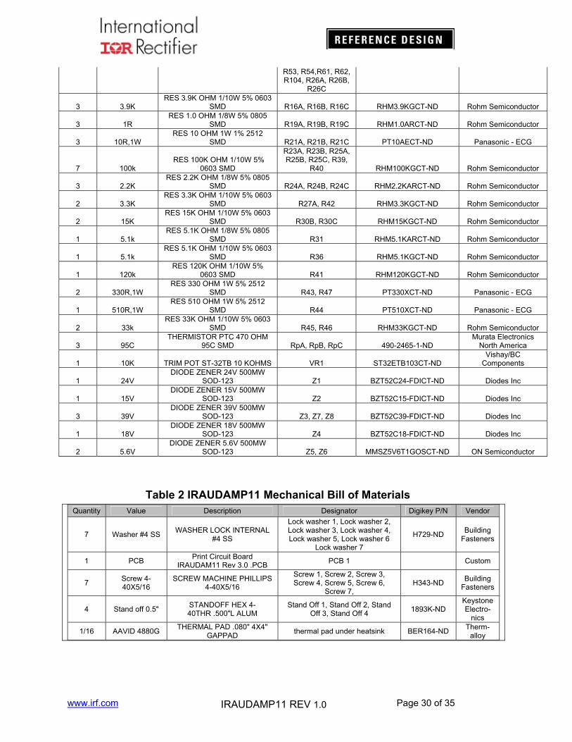
Table 2 IRAUDAMP11 Mechanical Bill of Materials Quantity Value Description Designator Digikey P/N Vendor
7 Washer #4 SS WASHER LOCK INTERNAL
#4 SS
Lock washer 1, Lock washer 2, Lock washer 3, Lock washer 4, Lock washer 5, Lock washer 6
Lock washer 7
H729-ND Building
Fasteners
1 PCB Print Circuit Board
IRAUDAM11 Rev 3.0 .PCB PCB 1 Custom
7 Screw 4-40X5/16
SCREW MACHINE PHILLIPS 4-40X5/16
Screw 1, Screw 2, Screw 3, Screw 4, Screw 5, Screw 6,
Screw 7, H343-ND
Building Fasteners
4 Stand off 0.5" STANDOFF HEX 4-40THR .500"L ALUM
Stand Off 1, Stand Off 2, Stand Off 3, Stand Off 4
1893K-ND Keystone Electro-
nics
1/16 AAVID 4880G THERMAL PAD .080" 4X4"
GAPPAD thermal pad under heatsink BER164-ND
Therm-alloy
www.irf.com Page 31 of 35 IRAUDAMP11 REV 1.0
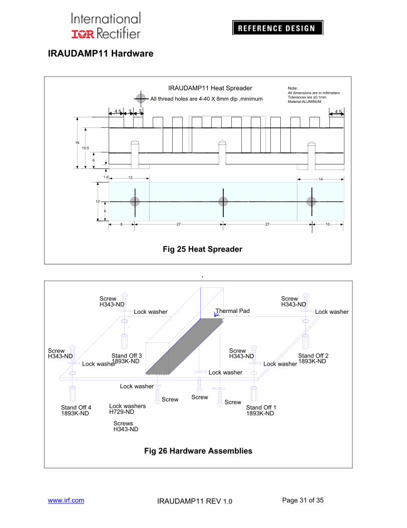
IRAUDAMP11 Hardware
4.5 4.53 3
108 27 27
12 141.6
6
10.5
16
6
12
IRAUDAMP11 Heat Spreader
All thread holes are 4-40 X 8mm dip ,minimum
Note:All dimensions are in millimetersTolerances are ±0.1mmMaterial:ALUMINUM
Fig 25 Heat Spreader
.
Fig 26 Hardware Assemblies
Screw
Screw H343-ND
Screws H343-ND
Stand Off 31893K-ND
ScrewStand Off 4 1893K-ND
Lock washers H729-ND
Lock washer
Lock washer
Stand Off 11893K-ND
Stand Off 21893K-ND
Lock washer
Screw H343-ND
Lock washer
Screw H343-ND
Lock washer
ScrewH343-ND
Lock washer
Screw
Thermal Pad Th l d

www.irf.com Page 32 of 35 IRAUDAMP11 REV 1.0
IRAUDAMP11 PCB Specifications PCB:
1. Two Layers SMT PCB with through holes 2. 1/16 thickness 3. 2/0 OZ Cu 4. FR4 material 5. 10 mil lines and spaces 6. Solder Mask to be Green enamel EMP110 DBG (CARAPACE) or Enthone Endplate
DSR-3241or equivalent. 7. Silk Screen to be white epoxy non conductive per IPC–RB 276 Standard. 8. All exposed copper must finished with TIN-LEAD Sn 60 or 63 for 100u inches thick. 9. Tolerance of PCB size shall be 0.010 –0.000 inches 10. Tolerance of all Holes is -.000 + 0.003” 11. PCB acceptance criteria as defined for class II PCB’S standards.
Gerber Files Apertures Description: All Gerber files stored in the attached CD-ROM were generated from Protel Altium Designer Altium Designer 6. Each file name extension means the following:
1. .gtl Top copper, top side 2. .gbl Bottom copper, bottom side 3. .gto Top silk screen 4. .gbo Bottom silk screen 5. .gts Top Solder Mask 6. .gbs Bottom Solder Mask 7. .gko Keep Out, 8. .gm1 Mechanical1 9. .gd1 Drill Drawing 10. .gg1 Drill locations 11. .txt CNC data 12. .apr Apertures data
Additional files for assembly that may not be related with Gerber files:
13. .pcb PCB file 14. .bom Bill of materials 15. .cpl Components locations 16. .sch Schematic 17. .csv Pick and Place Components 18. .net Net List 19. .bak Back up files 20. .lib PCB libraries

www.irf.com Page 33 of 35 IRAUDAMP11 REV 1.0
Fig 27 IRAUDAMP11 PCB Top Overlay (Top View)

www.irf.com Page 34 of 35 IRAUDAMP11 REV 1.0
Fig 28 IRAUDAMP11 PCB Bottom Layer (Top View)

www.irf.com Page 35 of 35 IRAUDAMP11 REV 1.0
Revision changes descriptions
Revision Changes description Date Rev 1.0 Released Oct, 08 2010
WORLD HEADQUARTERS: 233 Kansas St., El Segundo, California 90245 Tel: (310) 252-7105
Data and specifications subject to change without notice. 01/29/2009