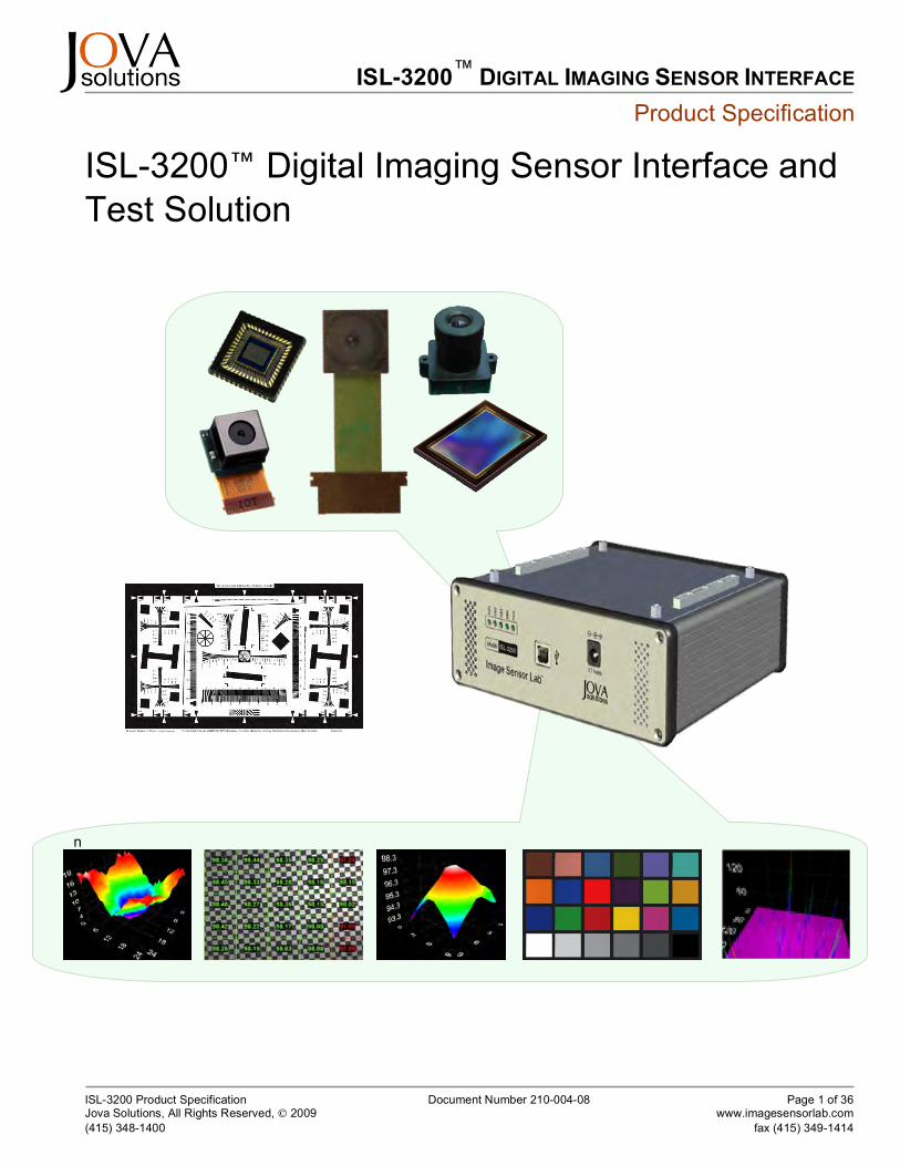
isl-3200 digital imaging sensor interface and test solution
TRANSCRIPT
ISL-3200™ DIGITAL IMAGING SENSOR INTERFACE Product Specification
ISL-3200 Product Specification Document Number 210-004-08 Page 1 of 36 Jova Solutions, All Rights Reserved, 2009 www.imagesensorlab.com (415) 348-1400 fax (415) 349-1414
ISL-3200™ Digital Imaging Sensor Interface and Test Solution
n

ISL-3200™ DIGITAL IMAGING SENSOR INTERFACE Product Specification
ISL-3200 Product Specification Document Number 210-004-08 Page 2 of 36
Table of Contents
1. INTRODUCTION .........................................................................................................................4 2. CONTACT INFORMATION .........................................................................................................4 3. PROPRIETARY INFORMATION.................................................................................................4 3.1 Software License ..........................................................................................................................................................4 3.2 Referenced Documents ...............................................................................................................................................4 4. HARDWARE FUNCTIONAL DESCRIPTION..............................................................................5 4.1 Overview ........................................................................................................................................................................5 4.2 Hardware Configuration Options...............................................................................................................................6 4.3 Physical Description ....................................................................................................................................................7 4.4 Test Interface.................................................................................................................................................................8
4.4.1 ISL-3200 vs. ISL-1600 Compatibility Considerations..........................................................................................10 4.5 Host Computer Interface ...........................................................................................................................................12
4.5.1 USB 2.0 HS Interface ............................................................................................................................................12 4.5.2 PCIe Interface ........................................................................................................................................................12
5. HARDWARE SPECIFICATIONS...............................................................................................13 5.1 Input Power Requirements .......................................................................................................................................13
5.1.1 Input Power Connections ......................................................................................................................................13 5.2 Output Power Specification......................................................................................................................................14
5.2.1 Output Power Overview ........................................................................................................................................14 5.2.2 PSIO, PSA, PSB, PSC, PSD (1.25V – 3.8V, 100 mA)........................................................................................15 5.2.3 PSE, PSF (0.6V – 1.8V, 600mA)..........................................................................................................................16 5.2.4 PSG, PSH (1.0V – 3.4V, 600mA) .........................................................................................................................17 5.2.5 PSU (0V – 10V, 500mA) .......................................................................................................................................18 5.2.6 PSX, PXY (1.224V – 3.3V, 150 mA) ....................................................................................................................19 5.2.7 Adaptor Power Output 1 (+3.3V) ..........................................................................................................................20 5.2.8 Additional Power Management Outputs ..............................................................................................................21
5.2.8.1 Adaptor 3.3V Output 2....................................................................................................................................21 5.2.8.2 PWM Open Drain Outputs 1 & 2 ...................................................................................................................21 5.2.8.3 LED PWM Open Drain Outputs 1 & 2 ...........................................................................................................22 5.2.8.4 RGB LED Open Drain Outputs 1 & 2 ............................................................................................................22 5.2.8.5 Bright White LED Driver Outputs 1 & 2 .........................................................................................................23
5.3 Sensor Communication.............................................................................................................................................24 5.3.1 I2C Bus Interface ...................................................................................................................................................24 5.3.2 SPI Bus Interface ...................................................................................................................................................25 5.3.3 UART Interface ......................................................................................................................................................25
5.4 Digital Signal Interface Specification......................................................................................................................26 5.4.1 Clocks .....................................................................................................................................................................29
5.4.1.1 Internal Clock Generation (OSCCLK and REFCLK) ....................................................................................29 5.4.1.2 Capture Clock “CAPCLK”...............................................................................................................................29
5.4.2 Synchronization Signals ........................................................................................................................................30 5.5 Static Digital Input and Output Control ..................................................................................................................30
Image Sensor Lab TM Digital Imaging Sensor Interface Product Specification
ISL-3200TM Product Specification Document Number 210-004-08 Page 3 of 36
5.6 Mechanical Specifications ........................................................................................................................................31 5.6.1 Top Down View......................................................................................................................................................31
5.7 Connector Specifications..........................................................................................................................................32 5.8 Environmental Specifications ..................................................................................................................................32 5.9 VOM Option .................................................................................................................................................................33
5.9.1 Measurement Bus..................................................................................................................................................33 5.9.1.1 2-Wire x 80 Analog Switch Matrix..................................................................................................................33
5.9.2 Sources and Loads................................................................................................................................................34 5.9.2.1 Programmable Pull-Up Resistor Voltage Source -- VDACApu ...................................................................34 5.9.2.2 Programmable Pull-Up Resistor -- 10KPU ...................................................................................................34 5.9.2.3 Programmable Voltage Source with Current Measurement -- VDACB ......................................................35 5.9.2.4 Programmable Current Sources – IDACA & IDACB....................................................................................35 5.9.2.5 Programmable Resistive Loads -- 10Kohm and 1Mohm.............................................................................35
5.9.3 Measurements .......................................................................................................................................................36 5.9.3.1 Voltage Measurements -- 12-bit and 24-bit VADC.......................................................................................36

ISL-3200™ DIGITAL IMAGING SENSOR INTERFACE Product Specification
ISL-3200 Product Specification Document Number 210-004-08 Page 4 of 36
1. INTRODUCTION The ISL-3200™ is a cost-effective combination of sensor interface, test electronics, and application software that provides complete communications, image capture, and characterization testing, of a wide variety of image sensors. The ISL software application offers scripting and plug-in functionality, allowing enhanced graphical user interfaces to specific image sensor models as well as customized image processing analysis and characterization testing routines. The ISL software application is pre-configured with a library of testing and characterization routines, as well as many of the processing tools that are typically needed for thorough evaluation and testing of image sensors.
2. CONTACT INFORMATION The primary contact for information regarding sales, support and technical information is:
Jova Solutions 965 Mission Street Suite 600 San Francisco, CA 94103 415-348-1400 415-348-1414 fax [email protected] http://www.jovasolutions.com
3. PROPRIETARY INFORMATION
This document contains information deemed proprietary. Information contained herein may be protected under patents, copyright, or by other lawful means. Use or reproduction of this document is restricted under the terms of the license.
3.1 SOFTWARE LICENSE The product described within this document contains licensed software that is protected under copyright law. You may not reverse engineer, decompile, disassemble, modify, translate, make any attempt to copy or discover the source code of the software, or create derivate works from the software.
Software © 2009, WireWorks West Inc. dba Jova Solutions, All Rights Reserved
3.2 REFERENCED DOCUMENTS Here are the documents related to the ISL-3200, which you may find useful:
Description Doc. No Company/Author Rev. Date
ISL-3200 Product Specification 210-0004-08 Jova Solutions 07/14/2009
ISL-3200 Basic User Manual 210-0001-08 Jova Solutions 07/14/2009
ISL-3200 Advanced Analysis Guide 210-0002-08 Jova Solutions 07/14/2009
ISL-3200 Quick Start Guide 210-0008-02 Jova Solutions 07/14/2009
ISL-3200 Test and Automation Suite Guide 210-0003-05 Jova Solutions 07/14/2009

ISL-3200™ DIGITAL IMAGING SENSOR INTERFACE Product Specification
ISL-3200 Product Specification Document Number 210-004-08 Page 5 of 36
4. HARDWARE FUNCTIONAL DESCRIPTION
4.1 OVERVIEW The Image Sensor Lab ISL-3200 is an electronic image sensor interface with built-in test and measurement capabilities. The ISL-3200 is a mixed signal device and includes programmable power supplies and oscillator, a flexible sensor image data frame capture capability. I2C, SPI, and UART sensor communication channels are also supplied.
• USB 2.0 HS Interface (450Mbps) • Optional External PCIe (2.5 Gbps) • Programmable power supplies with voltage and
current measurement • Programmable master clock oscillator up to 136 MHz • 8 and 16 bit data capture into on-board memory • 32 Mbytes on-board memory for USB version, 128
Mbytes for PCIe version • Additional digital I/O • I2C, SPI, and UART sensor communications provided • Sensor signal voltage translation buffers with
programmable isolation • Built-in timer/counter • Optional embedded Volt-Ohm Meter with 2x80 switch matrix (Short/Open test capable) • Image Sensor Lab ISL-3200 Product Specification • Drivers and automation API available
Image Sensors are typically connected to the ISL-3200 by a custom adapter board, which is mounted to the top of the ISL-3200, using the two 180-pin high density connectors, as shown in the figure above.
The ISL-3200 is housed in a compact 160mm x 160mm x 53 mm enclosure that is connected to the host computer via a USB 2.0 HS cable (or optional External PCIe cable).
A block diagram showing the major components of the ISL-3200 is shown below The image sensor is connected to internal circuitry through voltage level translation buffers in order to accommodate image sensors operating with different signal levels. An FPGA is used for the frame capture logic as well as the built-in timer/counter measurements. A microcontroller is also used within the ISL-3200 to control and coordinate the various devices, including the power management circuitry. A variety of power supplies is included with voltage and current measurement capability. A high-resolution current measurement mode is available for measuring standby currents in the µA range.
ISL-3200TM
Cost-Effective Image Sensor Testing Isolation and
Level-Shifting Buffers
Image Sensor or Camera Module
Sensor Power Sync
Image Data Sensor I2C/SPI Additional I/O
Pixel Clock
Master Clock
USB 2.0 HS or PCI Express
FPGA
Power Management Subsystem
Microprocessor
Image Memory
160-pin high-density connectors
Customer-specific Adapter Board
ISL-3200™ DIGITAL IMAGING SENSOR INTERFACE Product Specification
ISL-3200 Product Specification Document Number 210-004-08 Page 6 of 36
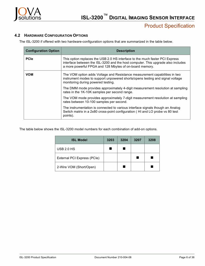
4.2 HARDWARE CONFIGURATION OPTIONS The ISL-3200 if offered with two hardware-configuration options that are summarized in the table below.
The table below shows the ISL-3200 model numbers for each combination of add-on options.
Configuration Option Description
PCIe This option replaces the USB 2.0 HS interface to the much faster PCI Express interface between the ISL-3200 and the host computer. This upgrade also includes a more powerful FPGA and 128 Mbytes of on-board memory.
VOM The VOM option adds Voltage and Resistance measurement capabilities in two instrument modes to support unpowered shorts/opens testing and signal voltage monitoring during powered testing.
The DMM mode provides approximately 4-digit measurement resolution at sampling rates in the 1K-10K samples per second range.
The VOM mode provides approximately 7-digit measurement resolution at sampling rates between 10-100 samples per second.
The instrumentation is connected to various interface signals though an Analog Switch matrix in a 2x80 cross-point configuration ( HI and LO probe vs 80 test points).
ISL Model 3203 3204 3207 3208
USB 2.0 HS
External PCI Express (PCIe)
2-Wire VOM (Short/Open)

Image Sensor Lab TM Digital Imaging Sensor Interface Product Specification
ISL-3200TM Product Specification Document Number 210-004-08 Page 7 of 36
4.3 PHYSICAL DESCRIPTION The ISL-3200 instrument is housed in a metal enclosure with connectors for power, communications, and image sensor connection. The overall size is 160mm wide by 160mm deep by 51mm high. Two 180-pin high-density connectors on the top of the ISL-3200 are used for sensor power and interface signals. The ISL-3200 is powered from an external +12VDC, 3 Amp minimum power source, via a 2.5mm center pin Power Plug (e.g., a 12V laptop style supply). The ISL-3200 is controlled via a USB 2.0 High Speed Interface or the optional PCIe High Speed Interface.

Image Sensor Lab TM Digital Imaging Sensor Interface Product Specification
ISL-3200TM Product Specification Document Number 210-004-08 Page 8 of 36
4.4 TEST INTERFACE The ISL-3200 Series Test Interface connections are detailed in the diagrams below.
J1 West J2 East Signal Pin Pin Signal Signal Pin Pin Signal GND 2 1 GND GND 2 1 GND
PSB_OUT 4 3 PSIO 4 3 PSA_OUT PSB_RTN 6 5 PSIO 6 5 PSA_RTN
8 7 ADPT_3V2_OUT ADPT_3V1_OUT 8 7 10 9 ADPT_3V2_GND ADPT_3V1_GND 10 9
PSD_OUT 12 11 PSF_OUT PSE_OUT 12 11 PSC_OUT PSD_RTN 14 13 PSF_RTN PSE_RTN 14 13 PSC_RTN
16 15 16 15 18 17 18 17
GND 20 19 GND GND 20 19 GND LED_PWM2_OUT 22 21 PSH_OUT PSG_OUT 22 21 LED_PWM1_OUT LED_PWM2_RTN 24 23 PSH_RTN PSG_RTN 24 23 LED_PWM1_RTN BRITE_LED2_OUT 26 25 26 25 BRITE_LED1_OUT BRITE_LED2_RTN 28 27 28 27 BRITE_LED1_RTN
30 29 30 29 RGB2_OUT 32 31 PWM2_OUT PWM1_OUT 32 31 RGB1_OUT
RGB2_RED_RTN 34 33 PWM2_RTN PWM1_RTN 34 33 RGB1_RED_RTN RGB2_GRN_RTN 36 35 PSY_OUT PSX OUT 36 35 RGB1_GRN_RTN RGB2_BLU_RTN 38 37 PSY_RTN PSX RTN 38 37 RGB1_BLU_RTN
GND 40 39 GND GND 40 39 GND
GND 42 41 GND GND 42 41 GND PSU_OUT 44 43 I2C_VREF SPI_SCK 44 43 PSU_RTN 46 45 I2C_SCL_RES SPI_SDO 46 45
PSU_OUT_Sense 48 47 I2C_SDA_RES SPI_SDI 48 47 PSU_RTN_Sense 50 49 I2C_SCL SPI_nSS 50 49
ABS_USER0 52 51 I2C_SDA SPI_nCS0 52 51 ABS_USER1 54 53 ADPT_I2C_SDA SPI_nCS1 54 53 ABS_USER2 56 55 ADPT_I2C_SCL SPI_nCS2 56 55 ABS_USER3 58 57 ADPT_I2C_VREF SPI_nCS3 58 57
GND 60 59 GND GND 60 59 GND ABS_PSU_OUT 62 61 REFCLK 62 61 ABS_PSU_RTN 64 63 PIXCLK ADPT_SPI_nCS0 64 63
66 65 PSIO ADPT_SPI_nCS1 66 65 68 67 ADPT_SPI_nCS2 68 67 70 69 ADPT_SPI_nCS3 70 69 72 71 UART_TX ADPT_SPI_nCS4 72 71 ADPT_SPI_nSS 74 73 UART_RX ADPT_SPI_nCS5 74 73 ADPT_SPI_SDI 76 75 UART_RTS ADPT_SPI_nCS6 76 75 ADPT_SPI_SCK 78 77 UART_CTS ADPT_SPI_nCS7 78 77 ADPT_SPI_SDO
GND 80 79 GND GND 80 79 GND
Continued Pins 81 through 160 Next Page Continued Pins 81 through 160
Next Page Notes: Gray – Reserved for Future Use. Do Not Connect to these pins. Yellow – Analog boundary scan test point.
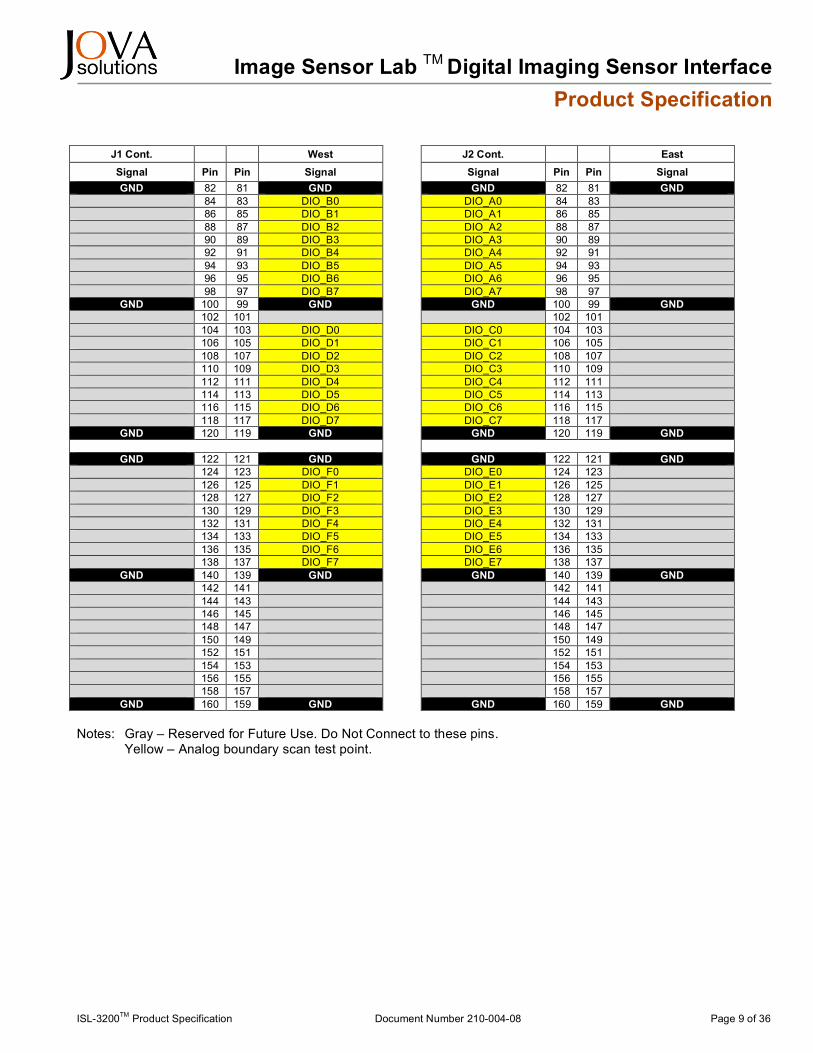
Image Sensor Lab TM Digital Imaging Sensor Interface Product Specification
ISL-3200TM Product Specification Document Number 210-004-08 Page 9 of 36
J1 Cont. West J2 Cont. East Signal Pin Pin Signal Signal Pin Pin Signal GND 82 81 GND GND 82 81 GND
84 83 DIO_B0 DIO_A0 84 83 86 85 DIO_B1 DIO_A1 86 85 88 87 DIO_B2 DIO_A2 88 87 90 89 DIO_B3 DIO_A3 90 89 92 91 DIO_B4 DIO_A4 92 91 94 93 DIO_B5 DIO_A5 94 93 96 95 DIO_B6 DIO_A6 96 95 98 97 DIO_B7 DIO_A7 98 97
GND 100 99 GND GND 100 99 GND 102 101 102 101 104 103 DIO_D0 DIO_C0 104 103 106 105 DIO_D1 DIO_C1 106 105 108 107 DIO_D2 DIO_C2 108 107 110 109 DIO_D3 DIO_C3 110 109 112 111 DIO_D4 DIO_C4 112 111 114 113 DIO_D5 DIO_C5 114 113 116 115 DIO_D6 DIO_C6 116 115 118 117 DIO_D7 DIO_C7 118 117
GND 120 119 GND GND 120 119 GND
GND 122 121 GND GND 122 121 GND 124 123 DIO_F0 DIO_E0 124 123 126 125 DIO_F1 DIO_E1 126 125 128 127 DIO_F2 DIO_E2 128 127 130 129 DIO_F3 DIO_E3 130 129 132 131 DIO_F4 DIO_E4 132 131 134 133 DIO_F5 DIO_E5 134 133 136 135 DIO_F6 DIO_E6 136 135 138 137 DIO_F7 DIO_E7 138 137
GND 140 139 GND GND 140 139 GND 142 141 142 141 144 143 144 143 146 145 146 145 148 147 148 147 150 149 150 149 152 151 152 151 154 153 154 153 156 155 156 155 158 157 158 157
GND 160 159 GND GND 160 159 GND Notes: Gray – Reserved for Future Use. Do Not Connect to these pins. Yellow – Analog boundary scan test point.

Image Sensor Lab TM Digital Imaging Sensor Interface Product Specification
ISL-3200TM Product Specification Document Number 210-004-08 Page 10 of 36
4.4.1 ISL-3200 vs. ISL-1600 Compatibility Considerations ISL-3200 power supplies PSA through PSD are similar in effective operating voltage range to an ISL-1600-PS01, however have half the maximum current.
In the ISL-1600, PSE, a PS01 type supply provides its output power to internal buffer circuitry as well, as being available for external use. In the ISL-3200, a separate PSIO supply provides power to internal buffers and is available as a voltage reference at the test interface. Other supplies that meet or exceed the PS01 type supply performance for most applications are available for use to provide PSE power.
The ISL-1600-PS03 type supply has been incorporated and is available as PSU.
To minimize ISL-1600 user efforts to transition to an ISL-3200 Series unit, an FPGA logic file is provided for use containing the ISL-1600 Capture Logic. The use of certain ISL-3200 signals are either fixed or prohibited.
The ISL-3200 Series Test Interface for ISL-1600 Compatibility is detailed in the diagrams below.
J1 West J2 East Signal Pin Pin Signal Signal Pin Pin Signal GND 2 1 GND GND 2 1 GND
PSB_OUT 4 3 PSIO 4 3 PSA_OUT PSB_RTN 6 5 PSIO 6 5 PSA_RTN
8 7 ADPT_3V2_OUT ADPT_3V1_OUT 8 7 10 9 ADPT_3V2_GND ADPT_3V1_GND 10 9
PSD_OUT 12 11 PSF_OUT PSE_OUT 12 11 PSC_OUT PSD_RTN 14 13 PSF_RTN PSE_RTN 14 13 PSC_RTN
16 15 16 15 18 17 18 17
GND 20 19 GND GND 20 19 GND LED_PWM2_OUT 22 21 PSH_OUT PSG_OUT 22 21 LED_PWM1_OUT LED_PWM2_RTN 24 23 PSH_RTN PSG_RTN 24 23 LED_PWM1_RTN BRITE_LED2_OUT 26 25 26 25 BRITE_LED1_OUT BRITE_LED2_RTN 28 27 28 27 BRITE_LED1_RTN
30 29 30 29 RGB2_OUT 32 31 PWM2_OUT PWM1_OUT 32 31 RGB1_OUT
RGB2_RED_RTN 34 33 PWM2_RTN PWM1_RTN 34 33 RGB1_RED_RTN RGB2_GRN_RTN 36 35 PSY_OUT PSX OUT 36 35 RGB1_GRN_RTN RGB2_BLU_RTN 38 37 PSY_RTN PSX RTN 38 37 RGB1_BLU_RTN
GND 40 39 GND GND 40 39 GND
GND 42 41 GND GND 42 41 GND PSU_OUT 44 43 I2C_VREF SPI_SCK 44 43 PSU_RTN 46 45 I2C_SCL_RES SPI_SDO 46 45
PSU_OUT_Sense 48 47 I2C_SDA_RES SPI_SDI 48 47 PSU_RTN_Sense 50 49 I2C_SCL SPI_nSS 50 49
ABS_USER0 52 51 I2C_SDA SPI_nCS0 52 51 ABS_USER1 54 53 ADPT_I2C_SDA SPI_nCS1 54 53 ABS_USER2 56 55 ADPT_I2C_SCL SPI_nCS2 56 55 ABS_USER3 58 57 ADPT_I2C_VREF SPI_nCS3 58 57
GND 60 59 GND GND 60 59 GND ABS_PSU_OUT 62 61 REFCLK 62 61 ABS_PSU_RTN 64 63 PIXCLK ADPT_SPI_nCS0 64 63
66 65 PSIO ADPT_SPI_nCS1 66 65 68 67 ADPT_SPI_nCS2 68 67 70 69 ADPT_SPI_nCS3 70 69 72 71 UART_TX ADPT_SPI_nCS4 72 71 ADPT_SPI_nSS 74 73 UART_RX ADPT_SPI_nCS5 74 73 ADPT_SPI_SDI 76 75 UART_RTS ADPT_SPI_nCS6 76 75 ADPT_SPI_SCK 78 77 UART_CTS ADPT_SPI_nCS7 78 77 ADPT_SPI_SDO
GND 80 79 GND GND 80 79 GND
Continued Pins 81 through 160 Next Page Continued Pins 81 through 160
Next Page
Notes: Gray – Reserved for Future Use. Do Not Connect to these pins. Yellow – Analog boundary scan test point.
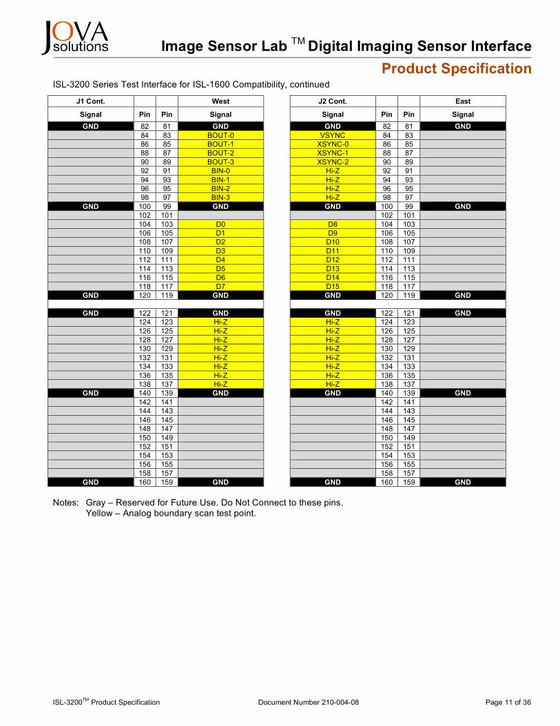
Image Sensor Lab TM Digital Imaging Sensor Interface Product Specification
ISL-3200TM Product Specification Document Number 210-004-08 Page 11 of 36
ISL-3200 Series Test Interface for ISL-1600 Compatibility, continued
J1 Cont. West J2 Cont. East
Signal Pin Pin Signal Signal Pin Pin Signal GND 82 81 GND GND 82 81 GND
84 83 BOUT-0 VSYNC 84 83 86 85 BOUT-1 XSYNC-0 86 85 88 87 BOUT-2 XSYNC-1 88 87 90 89 BOUT-3 XSYNC-2 90 89 92 91 BIN-0 Hi-Z 92 91 94 93 BIN-1 Hi-Z 94 93 96 95 BIN-2 Hi-Z 96 95 98 97 BIN-3 Hi-Z 98 97
GND 100 99 GND GND 100 99 GND 102 101 102 101 104 103 D0 D8 104 103 106 105 D1 D9 106 105 108 107 D2 D10 108 107 110 109 D3 D11 110 109 112 111 D4 D12 112 111 114 113 D5 D13 114 113 116 115 D6 D14 116 115 118 117 D7 D15 118 117
GND 120 119 GND GND 120 119 GND
GND 122 121 GND GND 122 121 GND 124 123 Hi-Z Hi-Z 124 123 126 125 Hi-Z Hi-Z 126 125 128 127 Hi-Z Hi-Z 128 127 130 129 Hi-Z Hi-Z 130 129 132 131 Hi-Z Hi-Z 132 131 134 133 Hi-Z Hi-Z 134 133 136 135 Hi-Z Hi-Z 136 135 138 137 Hi-Z Hi-Z 138 137
GND 140 139 GND GND 140 139 GND 142 141 142 141 144 143 144 143 146 145 146 145 148 147 148 147 150 149 150 149 152 151 152 151 154 153 154 153 156 155 156 155 158 157 158 157
GND 160 159 GND GND 160 159 GND Notes: Gray – Reserved for Future Use. Do Not Connect to these pins. Yellow – Analog boundary scan test point.

Image Sensor Lab TM Digital Imaging Sensor Interface Product Specification
ISL-3200TM Product Specification Document Number 210-004-08 Page 12 of 36
4.5 HOST COMPUTER INTERFACE The ISL-3200 default hardware configuration includes a USB 2.0 HS interface and is described below in paragraph 4.5.1. An optional External PCI Express interface is also available and comes as a replacement to the USB interface (i.e., one or the other, but not both).
4.5.1 USB 2.0 HS Interface
The USB is compliant with the USB.org specification revision 2.0 High-Speed requirements.
The ISL-3200 is a USB ‘Self-Powered’ device - it does not draw any power from the USB +5V line.
The USB ground signal line is tied to ISL-3200 common ground, external power adaptor DC return, and enclosure.
4.5.2 PCIe Interface
This option replaces the USB interface with a much faster PCIe interface, and provides a larger more powerful FPGA and 128MByte RAM for the image data buffer. The PCIe interface uses a standard Molex 74150-0001 connector, which can be connected to the External PCIe connectors that are provided on most laptop computers. An inexpensive simple PCIe plug-in card is also available for desktop and workstation computers.
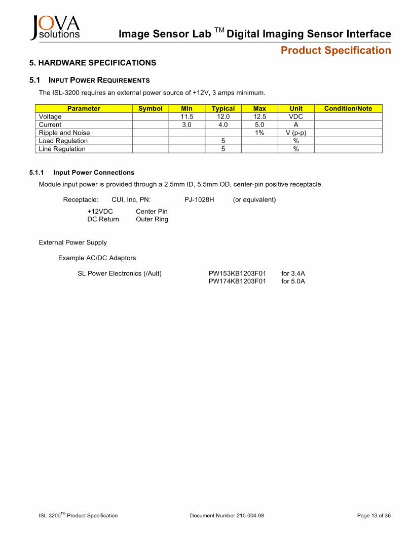
Image Sensor Lab TM Digital Imaging Sensor Interface Product Specification
ISL-3200TM Product Specification Document Number 210-004-08 Page 13 of 36
5. HARDWARE SPECIFICATIONS
5.1 INPUT POWER REQUIREMENTS The ISL-3200 requires an external power source of +12V, 3 amps minimum.
Parameter Symbol Min Typical Max Unit Condition/Note Voltage 11.5 12.0 12.5 VDC Current 3.0 4.0 5.0 A Ripple and Noise 1% V (p-p) Load Regulation 5 % Line Regulation 5 %
5.1.1 Input Power Connections
Module input power is provided through a 2.5mm ID, 5.5mm OD, center-pin positive receptacle.
Receptacle: CUI, Inc, PN: PJ-1028H (or equivalent)
+12VDC Center Pin DC Return Outer Ring
External Power Supply
Example AC/DC Adaptors
SL Power Electronics (/Ault) PW153KB1203F01 for 3.4A PW174KB1203F01 for 5.0A
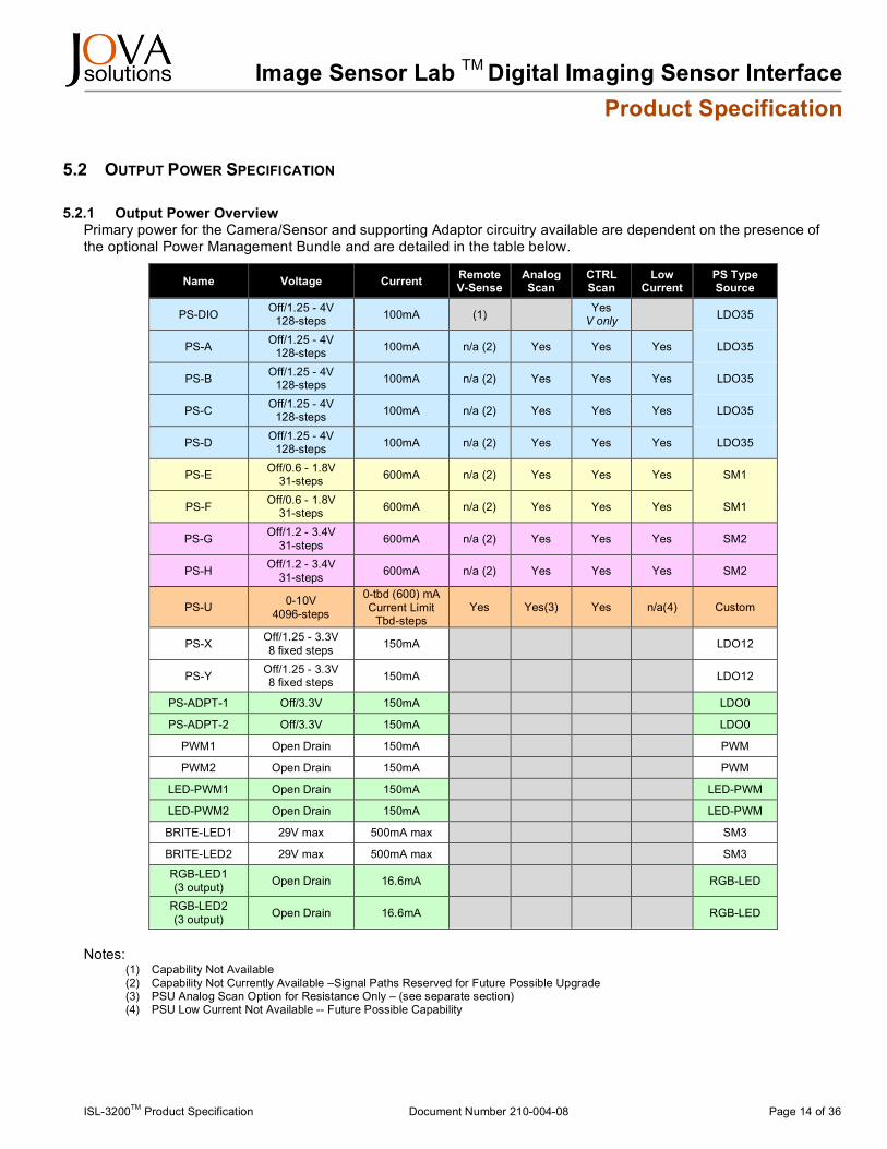
Image Sensor Lab TM Digital Imaging Sensor Interface Product Specification
ISL-3200TM Product Specification Document Number 210-004-08 Page 14 of 36
5.2 OUTPUT POWER SPECIFICATION
5.2.1 Output Power Overview Primary power for the Camera/Sensor and supporting Adaptor circuitry available are dependent on the presence of the optional Power Management Bundle and are detailed in the table below.
Name Voltage Current Remote V-Sense
Analog Scan
CTRL Scan
Low Current
PS Type Source
PS-DIO Off/1.25 - 4V 128-steps 100mA (1) Yes
V only LDO35
PS-A Off/1.25 - 4V 128-steps 100mA n/a (2) Yes Yes Yes LDO35
PS-B Off/1.25 - 4V 128-steps 100mA n/a (2) Yes Yes Yes LDO35
PS-C Off/1.25 - 4V 128-steps 100mA n/a (2) Yes Yes Yes LDO35
PS-D Off/1.25 - 4V 128-steps 100mA n/a (2) Yes Yes Yes LDO35
PS-E Off/0.6 - 1.8V 31-steps 600mA n/a (2) Yes Yes Yes SM1
PS-F Off/0.6 - 1.8V 31-steps 600mA n/a (2) Yes Yes Yes SM1
PS-G Off/1.2 - 3.4V 31-steps 600mA n/a (2) Yes Yes Yes SM2
PS-H Off/1.2 - 3.4V 31-steps 600mA n/a (2) Yes Yes Yes SM2
PS-U 0-10V 4096-steps
0-tbd (600) mA Current Limit
Tbd-steps Yes Yes(3) Yes n/a(4) Custom
PS-X Off/1.25 - 3.3V 8 fixed steps 150mA LDO12
PS-Y Off/1.25 - 3.3V 8 fixed steps 150mA LDO12
PS-ADPT-1 Off/3.3V 150mA LDO0
PS-ADPT-2 Off/3.3V 150mA LDO0
PWM1 Open Drain 150mA PWM
PWM2 Open Drain 150mA PWM
LED-PWM1 Open Drain 150mA LED-PWM
LED-PWM2 Open Drain 150mA LED-PWM
BRITE-LED1 29V max 500mA max SM3
BRITE-LED2 29V max 500mA max SM3
RGB-LED1 (3 output) Open Drain 16.6mA RGB-LED
RGB-LED2 (3 output) Open Drain 16.6mA RGB-LED
Notes:
(1) Capability Not Available (2) Capability Not Currently Available –Signal Paths Reserved for Future Possible Upgrade (3) PSU Analog Scan Option for Resistance Only – (see separate section) (4) PSU Low Current Not Available -- Future Possible Capability

Image Sensor Lab TM Digital Imaging Sensor Interface Product Specification
ISL-3200TM Product Specification Document Number 210-004-08 Page 15 of 36
5.2.2 PSIO, PSA, PSB, PSC, PSD (1.25V – 3.8V, 100 mA)
• High-resolution low-frequency measurements of output voltage and current, and remote voltage sensing, are supported.
• Medium-resolution medium-frequency measurements of output voltage and current, and remote voltage sensing, are supported.
Note: For proper digital signal operation, both PSIO and PS wired for powering camera/sensor digital IO should be programmed to output the same voltage levels.
A mechanical relay, 50mOHMS max, is used for the output connect/disconnect (excluding PSIO).

Image Sensor Lab TM Digital Imaging Sensor Interface Product Specification
ISL-3200TM Product Specification Document Number 210-004-08 Page 16 of 36
5.2.3 PSE, PSF (0.6V – 1.8V, 600mA)
• High-resolution low-frequency measurements of output voltage and current, and remote voltage sense, are supported.
• Medium-resolution medium-frequency measurements of output voltage and current, and remote voltage sense, are supported.
A mechanical relay, 50mOHMS max, is used for the output connect/disconnect.
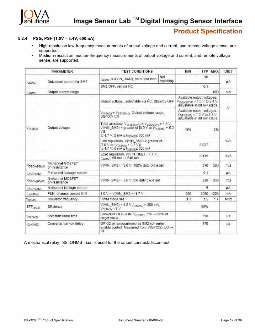
Image Sensor Lab TM Digital Imaging Sensor Interface Product Specification
ISL-3200TM Product Specification Document Number 210-004-08 Page 17 of 36
5.2.4 PSG, PSH (1.0V – 3.4V, 600mA)
• High-resolution low-frequency measurements of output voltage and current, and remote voltage sense, are supported.
• Medium-resolution medium-frequency measurements of output voltage and current, and remote voltage sense, are supported.
A mechanical relay, 50mOHMS max, is used for the output connect/disconnect.
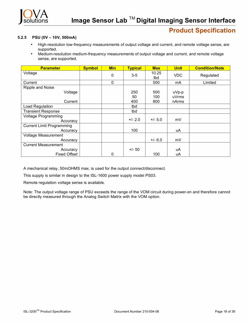
Image Sensor Lab TM Digital Imaging Sensor Interface Product Specification
ISL-3200TM Product Specification Document Number 210-004-08 Page 18 of 36
5.2.5 PSU (0V – 10V, 500mA)
• High-resolution low-frequency measurements of output voltage and current, and remote voltage sense, are supported.
• Medium-resolution medium-frequency measurements of output voltage and current, and remote voltage sense, are supported.
Parameter Symbol Min Typical Max Unit Condition/Note
Voltage 0 3-5 10.25 tbd VDC Regulated
Current 0 500 mA Limited Ripple and Noise
Voltage
Current
250 50
400
500 100 800
uVp-p uVrms nArms
Load Regulation tbd Transient Response tbd Voltage Programming
Accuracy +/- 2.0 +/- 5.0 mV
Current Limit Programming Accuracy
100 uA
Voltage Measurement Accuracy
+/- 6.0
mV
Current Measurement Accuracy
Fixed Offset
0
+/- 50
100
uA uA
A mechanical relay, 50mOHMS max, is used for the output connect/disconnect.
This supply is similar in design to the ISL-1600 power supply model PS03.
Remote regulation voltage sense is available. Note: The output voltage range of PSU exceeds the range of the VOM circuit during power-on and therefore cannot be directly measured through the Analog Switch Matrix with the VOM option.
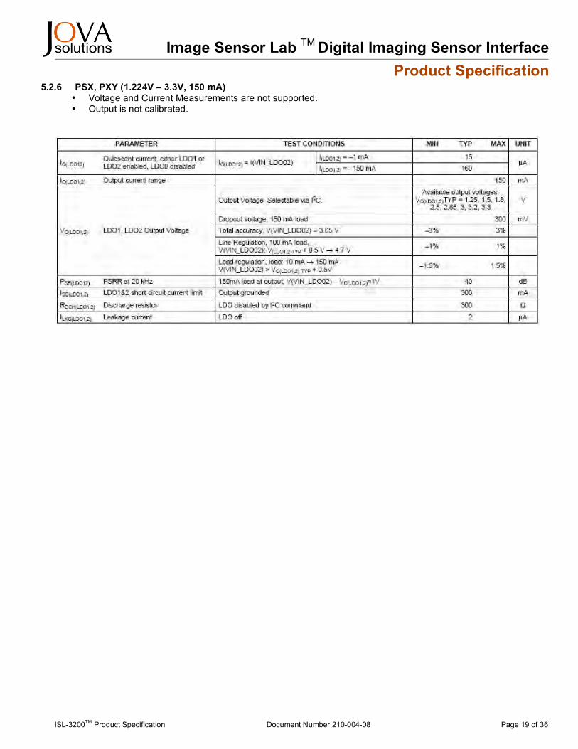
Image Sensor Lab TM Digital Imaging Sensor Interface Product Specification
ISL-3200TM Product Specification Document Number 210-004-08 Page 19 of 36
5.2.6 PSX, PXY (1.224V – 3.3V, 150 mA) • Voltage and Current Measurements are not supported. • Output is not calibrated.
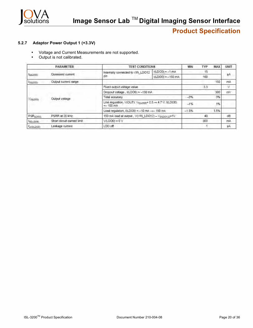
Image Sensor Lab TM Digital Imaging Sensor Interface Product Specification
ISL-3200TM Product Specification Document Number 210-004-08 Page 20 of 36
5.2.7 Adaptor Power Output 1 (+3.3V)
• Voltage and Current Measurements are not supported. • Output is not calibrated.

Image Sensor Lab TM Digital Imaging Sensor Interface Product Specification
ISL-3200TM Product Specification Document Number 210-004-08 Page 21 of 36
5.2.8 Additional Power Management Outputs
• Voltage and Current Measurements are not supported. • Outputs are not calibrated.
5.2.8.1 Adaptor 3.3V Output 2
5.2.8.2 PWM Open Drain Outputs 1 & 2

Image Sensor Lab TM Digital Imaging Sensor Interface Product Specification
ISL-3200TM Product Specification Document Number 210-004-08 Page 22 of 36
5.2.8.3 LED PWM Open Drain Outputs 1 & 2
5.2.8.4 RGB LED Open Drain Outputs 1 & 2

Image Sensor Lab TM Digital Imaging Sensor Interface Product Specification
ISL-3200TM Product Specification Document Number 210-004-08 Page 23 of 36
5.2.8.5 Bright White LED Driver Outputs 1 & 2
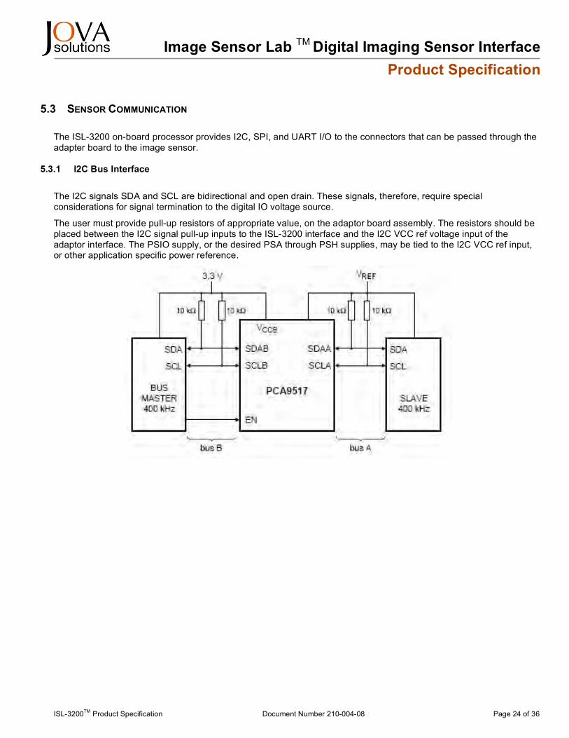
Image Sensor Lab TM Digital Imaging Sensor Interface Product Specification
ISL-3200TM Product Specification Document Number 210-004-08 Page 24 of 36
5.3 SENSOR COMMUNICATION The ISL-3200 on-board processor provides I2C, SPI, and UART I/O to the connectors that can be passed through the adapter board to the image sensor.
5.3.1 I2C Bus Interface
The I2C signals SDA and SCL are bidirectional and open drain. These signals, therefore, require special considerations for signal termination to the digital IO voltage source.
The user must provide pull-up resistors of appropriate value, on the adaptor board assembly. The resistors should be placed between the I2C signal pull-up inputs to the ISL-3200 interface and the I2C VCC ref voltage input of the adaptor interface. The PSIO supply, or the desired PSA through PSH supplies, may be tied to the I2C VCC ref input, or other application specific power reference.

Image Sensor Lab TM Digital Imaging Sensor Interface Product Specification
ISL-3200TM Product Specification Document Number 210-004-08 Page 25 of 36
5.3.2 SPI Bus Interface
The Serial Peripheral Interface (SPI) sub-system supports full-duplex synchronous serial communications. Primary features of the SPI sub-system are:
• Separate SPI signal pins for Camera/UUT and Adaptor use • Camera SPI signal levels are variable with programmed setting of PSIO. (see paragraph 5.4) • Adaptor SPI signal levels at 3.3v • Four (4) Camera Chip Select Signals (negative true) • Eight (8) Adaptor Chip Select Signals (negative true) • SCK Frequency range, 39.0625 KHz to 20 MHz
5.3.3 UART Interface The Universal Asynchronous Receiver Transmitter (UART) sub-system supports full-duplex serial communications, and can be configured to support hardware flow control via CTS and RTS signals. Primary features of the UART sub-system are:
• Full-Duplex 8 or 9-bit transmission through TX and RX signal pins. • Even, Odd or No Parity options (for 8-bit data). • One or Two Stop bits. • Hardware Flow Control option with CTS and RTS signal pins. • UART Baud Rate range, 19.0735 bps to 5 Mbps. • Parity, Framing Error Detection • 1K Byte Receive Buffer • 3.3V signal level standard, optional open drain with external pull up to up to 5V.
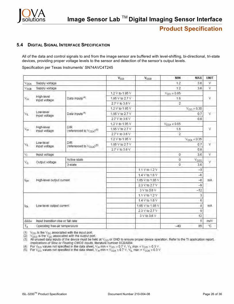
Image Sensor Lab TM Digital Imaging Sensor Interface Product Specification
ISL-3200TM Product Specification Document Number 210-004-08 Page 26 of 36
5.4 DIGITAL SIGNAL INTERFACE SPECIFICATION All of the data and control signals to and from the image sensor are buffered with level-shifting, bi-directional, tri-state devices, providing proper voltage levels to the sensor and detection of the sensor’s output levels.
Specification per Texas Instruments’ SN74AVC4T245

Image Sensor Lab TM Digital Imaging Sensor Interface Product Specification
ISL-3200TM Product Specification Document Number 210-004-08 Page 27 of 36
Image Sensor Lab TM Digital Imaging Sensor Interface Product Specification
ISL-3200TM Product Specification Document Number 210-004-08 Page 28 of 36
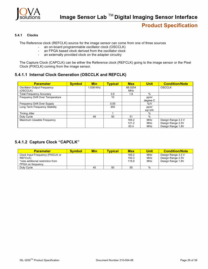
Image Sensor Lab TM Digital Imaging Sensor Interface Product Specification
ISL-3200TM Product Specification Document Number 210-004-08 Page 29 of 36
5.4.1 Clocks
The Reference clock (REFCLK) source for the image sensor can come from one of three sources
- an on-board programmable oscillator clock (OSCCLK) - an FPGA based clock derived from the oscillator clock - an externally provided clock on the adapter circuitry
The Capture Clock (CAPCLK) can be either the Reference clock (REFCLK) going to the image sensor or the Pixel Clock (PIXCLK) coming from the image sensor.
5.4.1.1 Internal Clock Generation (OSCCLK and REFCLK)
Parameter Symbol Min Typical Max Unit Condition/Note Oscillator Output Frequency (OSCCLK)
1.039 KHz 68.0254 MHz
OSCCLK
Total Frequency Accuracy 0.5 1.6 % Frequency Drift Over Temperature 10 ppm/
degree C
Frequency Drift Over Supply 0.05 %/V Long Term Frequency Stability 300 ppm/
sqr kHr
Timing Jitter 1 % Duty Cycle 49 50 51 % Maximum Useable Frequency 165.2
121.2 63.4
MHz MHz MHz
Design Range 3.3 V Design Range 2.5V Design Range 1.8V
5.4.1.2 Capture Clock “CAPCLK”
Parameter Symbol Min Typical Max Unit Condition/Note Clock Input Frequency (PIXCLK or REFCLK) *note additional restriction from FPGA on frequency
165.2 150.3 116.9
MHz MHz MHz
Design Range 3.3 V Design Range 2.5V Design Range 1.8V
Duty Cycle 45 50 55 %
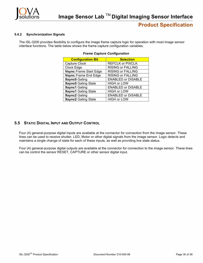
Image Sensor Lab TM Digital Imaging Sensor Interface Product Specification
ISL-3200TM Product Specification Document Number 210-004-08 Page 30 of 36
5.4.2 Synchronization Signals
The ISL-3200 provides flexibility to configure the image frame capture logic for operation with most image sensor interface functions. The table below shows the frame capture configuration variables.
Frame Capture Configuration
Configuration Bit Selection Capture Clock REFCLK or PIXCLK Clock Edge RISING or FALLING Vsync Frame Start Edge RISING or FALLING Vsync Frame End Edge RISING or FALLING Xsync0 Gating ENABLED or DISABLE Xsync0 Gating State HIGH or LOW Xsync1 Gating ENABLED or DISABLE Xsync1 Gating State HIGH or LOW Xsync2 Gating ENABLED or DISABLE Xsync2 Gating State HIGH or LOW
5.5 STATIC DIGITAL INPUT AND OUTPUT CONTROL Four (4) general-purpose digital inputs are available at the connector for connection from the image sensor. These lines can be used to receive shutter, LED, Motor or other digital signals from the image sensor. Logic detects and maintains a single change of state for each of these inputs, as well as providing live state status. Four (4) general-purpose digital outputs are available at the connector for connection to the image sensor. These lines can be control the sensor RESET, CAPTURE or other sensor digital input.

Image Sensor Lab TM Digital Imaging Sensor Interface Product Specification
ISL-3200TM Product Specification Document Number 210-004-08 Page 31 of 36
5.6 MECHANICAL SPECIFICATIONS 5.6.1 Top Down View
Parameter Symbol Min Typical Max Unit Condition/Note Size
Length Width
Height
160 160 51
mm mm mm
Excluding optional mounting brackets or feet.
Weight 32 Ounces
ISL-3200™ DIGITAL IMAGING SENSOR INTERFACE Product Specification
ISL-3200 Product Specification Document Number 210-004-08 Page 32 of 36
5.7 CONNECTOR SPECIFICATIONS Module input power is provided through a 2.5mm OD center pin receptacle.
Receptacle: Switchcraft PN: RAPC712 (or equivalent) Pin-1 +12VDC Center Pin Pin-2 DC Return Outer Ring
Input Power Mating Connector
Plug: Switchcraft PN: 760 CUI, Inc. PN: PP3-002B
The ISL-3200 test interface connector pins are detailed in (paragraph 4.4). The mating connector (used on the adapter boards) is a SAMTEC QSE-080-01-F-D-A.
5.8 ENVIRONMENTAL SPECIFICATIONS
Parameter Symbol Min Typical Max Unit Condition/Note Temperature 0 40 C Humidity tbd % Non-Condensing Altitude 10,000 ft Airflow
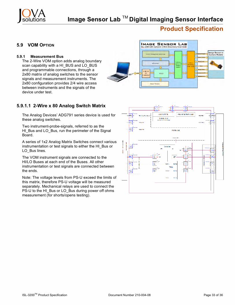
Image Sensor Lab TM Digital Imaging Sensor Interface Product Specification
ISL-3200TM Product Specification Document Number 210-004-08 Page 33 of 36
5.9 VOM OPTION
5.9.1 Measurement Bus The 2-Wire VOM option adds analog boundary scan capability with a HI_BUS and LO_BUS and programmable connections, through a 2x80 matrix of analog switches to the sensor signals and measurement instruments. The 2x80 configuration provides 2/4 wire access between instruments and the signals of the device under test.
5.9.1.1 2-Wire x 80 Analog Switch Matrix The Analog Devices’ ADG791 series device is used for these analog switches.
Two instrument-probe-signals, referred to as the HI_Bus and LO_Bus, run the perimeter of the Signal Board.
A series of 1x2 Analog Matrix Switches connect various instrumentation or test signals to either the HI_Bus or LO_Bus lines.
The VOM instrument signals are connected to the HI/LO Buses at each end of the Buses. All other instrumentation or test signals are connected between the ends.
Note: The voltage levels from PS-U exceed the limits of this matrix, therefore PS-U voltage will be measured separately. Mechanical relays are used to connect the PS-U to the HI_Bus or LO_Bus during power off ohms measurement (for shorts/opens testing).

Image Sensor Lab TM Digital Imaging Sensor Interface Product Specification
ISL-3200TM Product Specification Document Number 210-004-08 Page 34 of 36
5.9.2 Sources and Loads
5.9.2.1 Programmable Pull-Up Resistor Voltage Source -- VDACApu
Parameter Symbol Min Typical Max Unit Condition/Note VDACA
Range Increment
Short-Circuit Current
0
1.22 30
3.8
VDC mV mA
Pull-Up POR Default
Range Increment
Current
99.0625
5.06k
39.0625
10.06k
5
Ohms
mA
5.9.2.2 Programmable Pull-Up Resistor -- 10KPU
Parameter Symbol Min Typical Max Unit Condition/Note 10K Pull-Up
POR Default Range
Increment Current
99.0625
5.06k
39.0625
10.06k
5
Ohms
mA
Image Sensor Lab TM Digital Imaging Sensor Interface Product Specification
ISL-3200TM Product Specification Document Number 210-004-08 Page 35 of 36
5.9.2.3 Programmable Voltage Source with Current Measurement -- VDACB
Parameter Symbol Min Typical Max Unit Condition/Note VDACB
Range Increment
Short-Circuit Current
0
1.22 30
3.8
VDC mV mA
Current Sense Range
Resolution
1u
100n
30m
A
Minimum target goals
5.9.2.4 Programmable Current Sources – IDACA & IDACB
Parameter Symbol Min Typical Max Unit Condition/Note IDAC Range-1
Range Increment
Voltage
2.0833
2.0833
531.25
3.8
uA uA V
Open Circuit
IDAC Range-2 Range
Increment Voltage
.004167
4.167
1.0625
3.8
mA uA V
Open Circuit
IDAC Range-3 Range
Increment Voltage
.008333
8.333
2.125
3.8
mA uA V
Open Circuit
5.9.2.5 Programmable Resistive Loads -- 10Kohm and 1Mohm
Parameter Symbol Min Typical Max Unit Condition/Note 10K Load
POR Default Range
Increment Current
99.0625
5.06k
39.0625
10.06k
5
Ohms
mA
1M Load POR Default
Range Increment
Current
3.96625k
500.06k
3.90625K
1.0M
500
Ohms
uA
Image Sensor Lab TM Digital Imaging Sensor Interface Product Specification
ISL-3200TM Product Specification Document Number 210-004-08 Page 36 of 36
5.9.3 Measurements
5.9.3.1 Voltage Measurements -- 12-bit and 24-bit VADC
Parameter Symbol Min Typical Max Unit Condition/Note 12-Bit VADC
Range Resolution
Sample Time (1000 points)
Sample Time (100 points)
0
805
3.8
580 80
VDC uV
mSEC
[1]
24-Bit VADC Range
Resolution
Sample Rate
0
596
30
3.8
32
VDC nV
Pts/Sec
[2]
Notes: [1] Based on use of “DMM Measure HL_Bus Voltage.vi” with standard Sample & Hold and Conversion Period settings (as used during product calibration). Faster sample times can be achieved at the expense of less accuracy or increased sample point set noise. [2] Based on use of standard ADC sampling settings (as used during product calibration). Faster sampling rates can be achieved at the expense of less accuracy or increased sample point set noise. 24-Bit ADC reading are continuously performed in the background and placed into circular storage buffers. Calls to return the contents of the circular buffer can be performed in less than 20ms. Calls to return new samples in the foreground (that is acquiring new samples not placed in the circular buffer) are returned at the sample rate.