isl6446ademo1z user guide - intersil.com · isl6446ademo1z electronic input dc load electronic ......
TRANSCRIPT

USER’S MANUAL
AN1822Rev 1.00
May 7, 2015
ISL6446ADEMO1ZDual Channel Step Down Regulator Evaluation Board
IntroductionThe ISL6446A is a high performance Dual PWM + Single Linear Controller. This device integrates complete control, monitoring and protection functions for two synchronous buck PWM controllers and one low power linear controller. Each PWM channel is switched 180° out-of-phase for reduced input ripple current and lower EMI.
The PWM controller uses voltage mode control for simple output regulation. The output can be regulated from 0.8*VIN down to the 0.6V reference voltage. Switching frequency is programmable from 100kHz to 2.5MHz, providing either a cost optimized or compact power solution.
The ISL6446ADEMO1Z demo board is designed as an easy to use, dual output, non-isolated power module featuring synchronous buck function. It is well suited for any applications that require high performance, small space and low cost. The ISL6446ADEMO1Z output voltage is preset to 3.3V and 5V targeting ATX power supply applications. Each channel is designed for up to 20A of output current. Total power of the demo board is limited by thermal conditions.
Evaluation Board Features• 12V input voltage
• Preset +5V and +3.3V output
• 20A output current each channel
• Two-in-1 PWM controller with out-of-phase operation
• Voltage-mode PWM control
• Efficiency up to 94.9%
• Prebias start-up
• Undervoltage lockout
• Output overcurrent protection
• Over-temperature protection
• fsw set at 280kHz
• Simple dual layer board design
FIGURE 1. ISL6446ADEMO1Z REV B BOARD FIGURE 2. ISL6446ADEMO1Z REV B BOARD BACKSIDE
Evaluation Board Specifications
SYMBOL PARAMETERTEST
CONDITIONS MIN TYP MAX UNIT
VIN Input Range Over IO range 10.8 13.2 V
VOUT1 Output Range Over IO range 4.8 5 5.2 V
IOUT1 Output Current From no load to full load
0 20 A
VOUT2 Output Range Over IO range 3.1 3.3 3.5 V
IOUT2 Output Current From no load to full load
0 20 A
AN1822 Rev 1.00 Page 1 of 12May 7, 2015

ISL6446ADEMO1Z
Table of ContentsIntroduction . . . . . . . . . . . . . . . . . . . . . . . . . . . . . . . . . . . . . . . . . . . . . . . . . . . . . . . . . . . . . . . . . . . . . . . . . . . . . . . . . . . . . . . . . . . . . . . . 1
Evaluation Board Features. . . . . . . . . . . . . . . . . . . . . . . . . . . . . . . . . . . . . . . . . . . . . . . . . . . . . . . . . . . . . . . . . . . . . . . . . . . . . . . . . . . . 1Evaluation Board Specifications . . . . . . . . . . . . . . . . . . . . . . . . . . . . . . . . . . . . . . . . . . . . . . . . . . . . . . . . . . . . . . . . . . . . . . . . . . . . . . . . . . . . .1
Terminal Functions . . . . . . . . . . . . . . . . . . . . . . . . . . . . . . . . . . . . . . . . . . . . . . . . . . . . . . . . . . . . . . . . . . . . . . . . . . . . . . . . . . . . . . . . . . 3
Undervoltage Lockout Circuit . . . . . . . . . . . . . . . . . . . . . . . . . . . . . . . . . . . . . . . . . . . . . . . . . . . . . . . . . . . . . . . . . . . . . . . . . . . . . . . . . 3
ISL6446ADEMO1Z Schematic . . . . . . . . . . . . . . . . . . . . . . . . . . . . . . . . . . . . . . . . . . . . . . . . . . . . . . . . . . . . . . . . . . . . . . . . . . . . . . . . . 5
PCB Layout . . . . . . . . . . . . . . . . . . . . . . . . . . . . . . . . . . . . . . . . . . . . . . . . . . . . . . . . . . . . . . . . . . . . . . . . . . . . . . . . . . . . . . . . . . . . . . . . . 6
ISL6446ADEMO1Z Bill of Materials. . . . . . . . . . . . . . . . . . . . . . . . . . . . . . . . . . . . . . . . . . . . . . . . . . . . . . . . . . . . . . . . . . . . . . . . . . . . . 7
ISL6446ADEMO1Z Test Report. . . . . . . . . . . . . . . . . . . . . . . . . . . . . . . . . . . . . . . . . . . . . . . . . . . . . . . . . . . . . . . . . . . . . . . . . . . . . . . . . 8
Efficiency Curves . . . . . . . . . . . . . . . . . . . . . . . . . . . . . . . . . . . . . . . . . . . . . . . . . . . . . . . . . . . . . . . . . . . . . . . . . . . . . . . . . . . . . . . . . . . . 9
Steady State Operation . . . . . . . . . . . . . . . . . . . . . . . . . . . . . . . . . . . . . . . . . . . . . . . . . . . . . . . . . . . . . . . . . . . . . . . . . . . . . . . . . . . . . . 9
Protection . . . . . . . . . . . . . . . . . . . . . . . . . . . . . . . . . . . . . . . . . . . . . . . . . . . . . . . . . . . . . . . . . . . . . . . . . . . . . . . . . . . . . . . . . . . . . . . . . 11
AN1822 Rev 1.00 Page 2 of 12May 7, 2015

ISL6446ADEMO1Z
Equipment Used for Validation• 12V/200W input power source
• Dual channel electronic load
Terminal Functions
Getting StartedUsing short twisted pair leads for any power connections and with all loads and power supplies off, refer to Figure 4 for the proper measurement and equipment setup. The Power Supply (PS) should not be connected to the circuit until told to do so in the following procedure.
When measuring the input or output voltage ripple, care must be taken to avoid a long ground lead on the oscilloscope probe. Measure the input or output voltage ripple by touching the probe tip directly across VOUT and GND terminals.
1. Keep the power supply and electronic load power off.
2. Connect the power supply; electronic load; voltage and current meters. Figure 4 shows while keeping the power supply and load shut down.
3. Turn on the power supply and set the input voltage to 12V. Monitor input current. If input current exceeds 100mA, turn off power supply and look for shorts.
4. Confirm VOUT1 = 3.3V, VOUT2 = 5V
5. Slowly increase the load on VOUT to 15A. Verify VOUT1 = 3.3V, VOUT2 = 5V
The board is now ready for operation.
Undervoltage Lockout CircuitThe ISL6446ADEMO1Z demo board includes as part of its circuitry a UVLO (Undervoltage Lockout) circuit that prevents it from starting up with VIN voltages less than about 7.8V. If you want to reduce the UVLO voltage, (resistor R12 in the schematic of the board) it needs to be reduced in value.
TABLE 1. TERMINAL FUNCTIONS
TERMINAL NAME DESCRIPTION
VIN The positive input voltage node to the module, which is referenced to common GND.
GND This is the common ground connection for the VIN and VOUT power connection.
5V The regulated positive 5V power output with respect to the GND node.
3.3V The regulated positive 3.3V power output with respect to the GND node.
FIGURE 3. TYPICAL APPLICATION DIAGRAM
VIN 3.3V
5VGND
ISL6446ADEMO1Z ELECTRONIC
INPUT DC
LOAD
ELECTRONICLOAD
POWER
FIGURE 4. CONNECTION DIAGRAM
VIN3.3V
5V
GND
ISL6446ADEMO1ZLOAD
LOAD
POWERSUPPLY
+
-
++
+
++
--
-
--
-
VV V
A+
A
A
AN1822 Rev 1.00 Page 3 of 12May 7, 2015
ISL6446ADEMO1Z
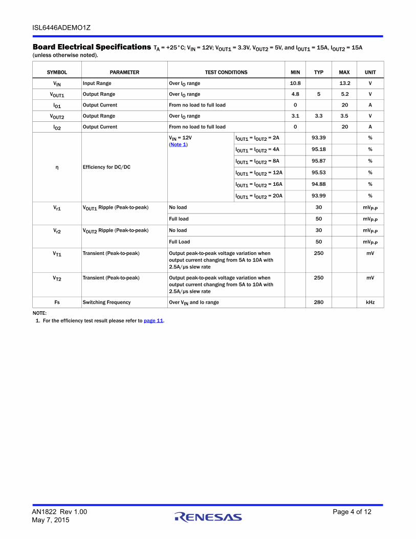
Board Electrical Specifications TA = +25°C; VIN = 12V; VOUT1 = 3.3V, VOUT2 = 5V, and IOUT1 = 15A, IOUT2 = 15A(unless otherwise noted).
SYMBOL PARAMETER TEST CONDITIONS MIN TYP MAX UNIT
VIN Input Range Over IO range 10.8 13.2 V
VOUT1 Output Range Over IO range 4.8 5 5.2 V
IO1 Output Current From no load to full load 0 20 A
VOUT2 Output Range Over IO range 3.1 3.3 3.5 V
IO2 Output Current From no load to full load 0 20 A
η Efficiency for DC/DC
VIN = 12V(Note 1)
IOUT1 = IOUT2 = 2A 93.39 %
IOUT1 = IOUT2 = 4A 95.18 %
IOUT1 = IOUT2 = 8A 95.87 %
IOUT1 = IOUT2 = 12A 95.53 %
IOUT1 = IOUT2 = 16A 94.88 %
IOUT1 = IOUT2 = 20A 93.99 %
Vr1 VOUT1 Ripple (Peak-to-peak) No load 30 mVP-P
Full load 50 mVP-P
Vr2 VOUT2 Ripple (Peak-to-peak) No load 30 mVP-P
Full Load 50 mVP-P
VT1 Transient (Peak-to-peak) Output peak-to-peak voltage variation when output current changing from 5A to 10A with 2.5A/µs slew rate
250 mV
VT2 Transient (Peak-to-peak) Output peak-to-peak voltage variation when output current changing from 5A to 10A with 2.5A/µs slew rate
250 mV
Fs Switching Frequency Over VIN and Io range 280 kHz
NOTE:1. For the efficiency test result please refer to page 11.
AN1822 Rev 1.00 Page 4 of 12May 7, 2015

AN
18
22R
ev 1.0
0P
age 5 of 1
2M
ay 7, 201
5
ISL6
446
AD
EM
O1Z
5VS 5V
3V3S 3V3
Title
Size Document Number<Doc>
<Title>
B
Title
Size Document Number<Doc>
<Title>
B
Title
Size Document Number<Doc>
<Title>
B
2
C30820UF
C2647UF
L4
0.2UH
L3
0.2UH
C4110UF
C24270UF
C2547UF
C2747UF
C23270UF
C4010UF
C1922UF
C2847UF
C29820UF
C2222UF
1
ISL6446ADEMO1Z Schematic
VIN
5V
FB2
SS2
VIN
3V3
FB2
3V3
VIN
5V
VIN SS1 SS2
VIN
PH1
PH2
PH1
VIN
PH2
VIN
L
2UH
C17 4.7UF
Q8
C14 0.01UF
C4220PF
C5 DNP
C2122UF
Q11
R615K
Q12
R1820
C431UF
C13 0.01UF
R568K
R210K
Q6
C16 1UF
R12100K
R110K
R9 1.3K
C8 0.47UF
R11 56K
R1451K
R415K
C31000PF
C9 1000PF
C421UF
C12 1000PF
R1920
Q9
C18 0.1UF
R8 10KQ7
Q42N7002
C2022UF
Q12N7002
C10 0.47UF
Q5
R16 0
C11 1000PF
C15 0.1UF
L
2UH
Q2NPN
Q32N7002
J1
CON10
123456789
10
C7 1000PF
R7 10K
C11000PF
R170
R139.1K
R3110K
C6 DNP
U1
ISL6446A
OCSET11
SS1/EN12
COMP13
FB14
RT5
SGND6
LCDR7
LCFB8
FB29
COMP210
SS2/EN211
OCSET212
PGOOD13
BOOT214
UGATE215
PHASE216
LGATE217
PGND18
VCC19
LGATE120
PHASE121
UGATE122
BOOT123
VIN24
R10 1.3K
R1520K
C2220PF
Q10
FIGURE 5. ISL6446ADEMO1Z SCHEMATIC

ISL6446ADEMO1Z
PCB Layout
FIGURE 6. SILK SCREEN TOP FIGURE 7. SILK SCREEN BOTTOM
FIGURE 8. PCB TOP FIGURE 9. PCB BOTTOM
AN1822 Rev 1.00 Page 6 of 12May 7, 2015

ISL6446ADEMO1Z
ISL6446ADEMO1Z Bill of Materials
MANUFACTURER PART QTYUNIT
SREFERENCE DESIGNATOR DESCRIPTION MANUFACTURER
ISL6446ADEMO1ZREVBPCB 1 ea. PWB-PCB, ISL6446ADEMO1Z, REVB, ROHS IMAGINEERING INC
06035C102KAT2A 6 ea. C1, C3, C7, C9, C11, C12
CAP, SMD, 0603, 1000pF, 50V, 10%, X7R, ROHS AVX
GRM39X7R103K050 2 ea. C13, C14 CAP, SMD, 0603, 0.01µF, 50V, 10%, X7R, ROHS MURATA
GRM39X7R104K025AD 2 ea. C15, C18 CAP, SMD, 0603, 0.1µF, 25V, 10%, X7R, ROHS MURATA
GRM188R61C105KA12D 3 ea. C16, C42, C43 CAP, SMD, 0603, 1µF, 16V, 10%, X5R, ROHS MURATA
GRM188R71H221KA01D 2 ea. C2, C4 CAP, SMD, 0603, 220pF, 50V, 10%, X7R, ROHS MURATA
C1608X7R1C474K 2 ea. C8, C10 CAP, SMD, 0603, 0.47µF, 16V, 10%, X7R, ROHS TDK
ECJ-2FB1C475K 1 ea. C17 CAP, SMD, 0805, 4.7µF, 16V, 10%, X5R, ROHS PANASONIC
C1206X7R100-106KNE 2 ea. C40, C41 CAP, SMD, 1206, 10µF, 10V, 10%, X7R, ROHS VENKEL
GRM32ER71C226KE18L 4 ea. C19, C20, C21, C22
CAP, SMD, 1210, 22µF,16V, 10%, X7R, ROHS MURATA
ECJ-4YB0J476M 4 ea. C25, C26, C27, C28
CAP, SMD, 1210, 47µF, 6.3V, 20%, X5R, ROHS PANASONIC
PA2509.201NL 2 ea. L3, L4 COIL-PWR INDUCTOR, SMD, 7X8.5, 0.2µH, 12%, 32A, 0.35mΩ, ROHS PULSE
RL80J821MDN1KX 2 ea. C29, C30 CAP, TH, RADIAL, 820µF, 6.3V, 20%, ALUM.POLYMER, 3.5mmLS, ROHS NICHICON
RL81C271MDN1KX 2 ea. C23, C24 CAP, TH, RADIAL, 270µF, 16V, 20%, ALUM.POLYMER, 3.5mmLS, ROHS NICHICON
SER2011-202MLB 2 ea. L1, L2 COIL-PWR INDUCTOR, SMD, 18.7X19.1, 2.0µH, 20%, 37A, 1.2mΩ, ROHS COILCRAFT
1-640385-0 1 ea. J1 CONN-HEADER, TH, 1X10, NYLON, R/A, 0.156mmPITCH, ROHS TE CONNECTIVITY
ISL6446AIAZ 1 ea. U1 IC-DUAL PWM/LINEAR CONTROLLER, 24P, QSOP, ROHS INTERSIL
2N7002-7-F 3 ea. Q1, Q3, Q4 TRANSISTOR, N-CHANNEL, 3LD, SOT-23, 60V, 115mA, ROHS DIODES, INC.
BSC010NE2LS 4 ea. Q7, Q8, Q11, Q12
TRANSIST-MOS, N-CHANNEL, 8P, PG-TDSON-8, 25V, 100A, ROHS INFINEON TECHNOLOGY
MMBT3904 1 ea. Q2 TRANSISTOR-NPN, SMD, SOT-23, 40V, 200mA, 350mW, ROHS FAIRCHILD
ERJ-3EKF20R0V 2 ea. R18, R19 RES, SMD, 0603, 20Ω, 1/10W, 1%, TF, ROHS PANASONIC
CR0603-10W-000T 2 ea. R16, R17 RES, SMD, 0603, 0Ω, 1/10W, TF, ROHS VENKEL
RK73H1JT1002F 4 ea. R1, R2, R7, R8 RES, SMD, 0603, 10k, 1/10W, 1%, TF, ROHS KOA
CR0603-10W-1003FT 1 ea. R12 RES, SMD, 0603, 100k, 1/10W, 1%, TF, ROHS VENKEL
ERJ-3EKF1103V 1 ea. R3 RES, SMD, 0603, 110k, 1/10W, 1%, TF, ROHS PANASONIC
CRCW06031K30FKTA 2 ea. R9, R10 RES, SMD, 0603, 1.3k, 1/10W, 1%, TF, ROHS VISHAY/DALE
ERJ-3EKF1502V 2 ea. R4, R6 RES, SMD, 0603, 15k, 1/10W, 1%, TF, ROHS PANASONIC
CR0603-10W-2002FT 1 ea. R15 RES, SMD, 0603, 20k, 1/10W, 1%, TF, ROHS VENKEL
RC0603FR-0751KL 1 ea. R14 RES, SMD, 0603, 51k, 1/10W, 1%, TF, ROHS YAGEO
ERJ-3EKF5602V 1 ea. R11 RES, SMD, 0603, 56k, 1/10W, 1%, TF, ROHS PANASONIC
RC0603FR-0768KL 1 ea. R5 RES, SMD, 0603, 68k, 1/10W, 1%, TF, ROHS YAGEO
CR0603-10W-9101FT 1 ea. R13 RES, SMD, 0603, 9.1k, 1/10W, 1%, TF, ROHS VENKEL
SJ-5003SPBL 4 ea. Bottom four corners
BUMPONS, 0.44inW x 0.20inH, DOMETOP, BLACK 3M
AN1822 Rev 1.00 Page 7 of 12May 7, 2015

ISL6446ADEMO1Z
ISL6446ADEMO1Z Test Report
FIGURE 10. START-UP FIGURE 11. START-UP
FIGURE 12. SHUTDOWN FIGURE 13. SHUTDOWN (UVLO VOLTAGE 7.4V)
5V
3.3V
VIN
VIN = 12V, NO LOAD START-UP
5V
3.3V
VIN
VIN = 12V, FULL LOAD START-UP
5V
3.3V
VIN
VIN = 12V, NO LOAD SHUTDOWN
5V
3.3V
VIN
VIN = 12V, FULL LOAD SHUTDOWN
AN1822 Rev 1.00 Page 8 of 12May 7, 2015

ISL6446ADEMO1Z
Efficiency Curves Input = 12VDC, Output = 5V/20A, 3.3V/20A.
FIGURE 14. EFFICIENCY vs OUTPUT POWER FIGURE 15. POWER LOSS vs OUTPUT POWER
FIGURE 16. OUTPUT LOAD REGULATION 5V FIGURE 17. OUTPUT LOAD REGULATION 3.3V
90
91
92
93
94
95
96
97
0 20 40 60 80 100 120 140 160 180
LOAD POWER (W)
EF
FIC
IEN
CY
(%
)
FULL LOAD 5V/20A, 3.3V/20A
0
1
2
3
4
5
6
7
8
9
10
11
12
0 20 40 60 80 100 120 140 160 180
LOAD POWER (W)
PO
WE
R L
OS
S (
W)
FULL LOAD 5V/20A, 3.3V/20A
4.96
4.97
4.98
4.99
5.00
5.01
5.02
5.03
5.04
0 2 4 6 8 10 12 14 16 18 20 22 OUTPUT CURRENT (A)
OU
TP
UT
VO
LT
AG
E (
V)
3.30
3.31
3.32
3.33
3.34
3.35
3.36
0 2 4 6 8 10 12 14 16 18 20 22 OUTPUT CURRENT (A)
OU
TP
UT
VO
LT
AG
E (
V)
Steady State Operation 1st stage LC (2µH + 2*47µF) + 2nd stage LC Output Filters (200nH + 820µF).
FIGURE 18. GATE DRIVER AND SWITCHING TRANSIENT FIGURE 19. GATE DRIVER AND SWITCHING TRANSIENT
PHASE
LGATE
NO LOAD, HIGH-SIDE MOS TURNS OFFLOW-SIDE MOS TURNS ONTHERE IS ENOUGH DEAD TIME
20A LOAD, HIGH-SIDE MOS TURNS OFFLOW-SIDE MOS TURNS ON
PHASE
LGATE
AN1822 Rev 1.00 Page 9 of 12May 7, 2015

ISL6446ADEMO1Z
FIGURE 20. GATE DRIVER AND SWITCHING TRANSIENT FIGURE 21. GATE DRIVER AND SWITCHING TRANSIENT
FIGURE 22. 5V NO LOAD OUTPUT RIPPLE 10mV FIGURE 23. 3.3V NO LOAD OUTPUT RIPPLE 13mV
FIGURE 24. 5V FULL LOAD OUTPUT RIPPLE 25mV FIGURE 25. 3.3V FULL LOAD OUTPUT RIPPLE 29mV
Steady State Operation 1st stage LC (2µH + 2*47µF) + 2nd stage LC Output Filters (200nH + 820µF). (Continued)
PHASE
NO LOAD, LOW-SIDE MOS TURNS OFFHIGH-SIDE MOS TURNS ONTHERE IS ENOUGH DEAD TIME
LGATE
PHASE
FULL LOAD, LOW-SIDE MOS TURNS OFFHIGH-SIDE MOS TURNS ONTHERE IS ENOUGH DEAD TIME
LGATE
PHASEPHASE
5V AC-COUPLED
VIN = 12V, NO LOAD OUTPUT RIPPLE
PHASE
NO LOAD, LOW SIDE MOS TURNS OFFHIGH SIDE MOS TURNS ONTHERE IS ENOUGH DEAD TIME
LGATE
PHASE
PHASE
VIN = 12V, NO LOAD OUTPUT RIPPLE
3.3V AC-COUPLED
PHASE
NO LOAD, LOW SIDE MOS TURNS OFFHIGH SIDE MOS TURNS ONTHERE IS ENOUGH DEAD TIME
LGATE
PHASE
PHASE
VIN = 12V, FULL LOAD OUTPUT RIPPLE
5V AC-COUPLED
PHASE
NO LOAD, LOW SIDE MOS TURNS OFFHIGH SIDE MOS TURNS ONTHERE IS ENOUGH DEAD TIME
LGATE
PHASE
PHASE
VIN = 12V, FULL LOAD OUTPUT RIPPLE
3.3V AC-COUPLED
AN1822 Rev 1.00 Page 10 of 12May 7, 2015

ISL6446ADEMO1Z
Output Transient Responses
FIGURE 26. 5A~10A, 2.5A/µs, PEAK-TO-PEAK RIPPLE 226mV FIGURE 27. 10A~15A, 2.5A/µs, PEAK-TO-PEAK RIPPLE 227mV
FIGURE 28. 5A~10A, 2.5A/µs, PEAK-TO-PEAK RIPPLE 200mV FIGURE 29. 10A~15A, 2.5A/µs, PEAK-TO-PEAK RIPPLE 205mV
5V OUTPUT50m/DIVAC-COUPLED 5VAC
20A LOAD, HIGH SIDE MOS TURNS OFFLOW SIDE MOS TURNS ON
5VAC
5V OUTPUT50mV/DIVAC-COUPLED
PHASE
NO LOAD, LOW SIDE MOS TURNS OFFHIGH SIDE MOS TURNS ONTHERE IS ENOUGH DEAD TIME
LGATE
3V OUTPUT50mV/DIVAC-COUPLED
PHASE
FULL LOAD, LOW SIDE MOS TURNS OFFHIGH SIDE MOS TURNS ONTHERE IS ENOUGH DEAD TIME
LGATE
3V OUTPUT50mV/DIVAC-COUPLED
Protection
FIGURE 30. OVERCURRENT PROTECTION FIGURE 31. OVERCURRENT PROTECTION
PHASE
IO
5V OCP PROTECTION
PHASE
IO
3.3V OCP PROTECTION
AN1822 Rev 1.00 Page 11 of 12May 7, 2015

http://www.renesas.comRefer to "http://www.renesas.com/" for the latest and detailed information.
Renesas Electronics America Inc.1001 Murphy Ranch Road, Milpitas, CA 95035, U.S.A.Tel: +1-408-432-8888, Fax: +1-408-434-5351Renesas Electronics Canada Limited9251 Yonge Street, Suite 8309 Richmond Hill, Ontario Canada L4C 9T3Tel: +1-905-237-2004Renesas Electronics Europe LimitedDukes Meadow, Millboard Road, Bourne End, Buckinghamshire, SL8 5FH, U.KTel: +44-1628-651-700, Fax: +44-1628-651-804Renesas Electronics Europe GmbHArcadiastrasse 10, 40472 Düsseldorf, Germany Tel: +49-211-6503-0, Fax: +49-211-6503-1327Renesas Electronics (China) Co., Ltd.Room 1709 Quantum Plaza, No.27 ZhichunLu, Haidian District, Beijing, 100191 P. R. ChinaTel: +86-10-8235-1155, Fax: +86-10-8235-7679Renesas Electronics (Shanghai) Co., Ltd.Unit 301, Tower A, Central Towers, 555 Langao Road, Putuo District, Shanghai, 200333 P. R. China Tel: +86-21-2226-0888, Fax: +86-21-2226-0999Renesas Electronics Hong Kong LimitedUnit 1601-1611, 16/F., Tower 2, Grand Century Place, 193 Prince Edward Road West, Mongkok, Kowloon, Hong KongTel: +852-2265-6688, Fax: +852 2886-9022Renesas Electronics Taiwan Co., Ltd.13F, No. 363, Fu Shing North Road, Taipei 10543, TaiwanTel: +886-2-8175-9600, Fax: +886 2-8175-9670Renesas Electronics Singapore Pte. Ltd.80 Bendemeer Road, Unit #06-02 Hyflux Innovation Centre, Singapore 339949Tel: +65-6213-0200, Fax: +65-6213-0300Renesas Electronics Malaysia Sdn.Bhd.Unit 1207, Block B, Menara Amcorp, Amcorp Trade Centre, No. 18, Jln Persiaran Barat, 46050 Petaling Jaya, Selangor Darul Ehsan, MalaysiaTel: +60-3-7955-9390, Fax: +60-3-7955-9510Renesas Electronics India Pvt. Ltd.No.777C, 100 Feet Road, HAL 2nd Stage, Indiranagar, Bangalore 560 038, IndiaTel: +91-80-67208700, Fax: +91-80-67208777Renesas Electronics Korea Co., Ltd.17F, KAMCO Yangjae Tower, 262, Gangnam-daero, Gangnam-gu, Seoul, 06265 KoreaTel: +82-2-558-3737, Fax: +82-2-558-5338
SALES OFFICES
© 2018 Renesas Electronics Corporation. All rights reserved.Colophon 7.0
(Rev.4.0-1 November 2017)
Notice
1. Descriptions of circuits, software and other related information in this document are provided only to illustrate the operation of semiconductor products and application examples. You are fully responsible for
the incorporation or any other use of the circuits, software, and information in the design of your product or system. Renesas Electronics disclaims any and all liability for any losses and damages incurred by
you or third parties arising from the use of these circuits, software, or information.
2. Renesas Electronics hereby expressly disclaims any warranties against and liability for infringement or any other claims involving patents, copyrights, or other intellectual property rights of third parties, by or
arising from the use of Renesas Electronics products or technical information described in this document, including but not limited to, the product data, drawings, charts, programs, algorithms, and application
examples.
3. No license, express, implied or otherwise, is granted hereby under any patents, copyrights or other intellectual property rights of Renesas Electronics or others.
4. You shall not alter, modify, copy, or reverse engineer any Renesas Electronics product, whether in whole or in part. Renesas Electronics disclaims any and all liability for any losses or damages incurred by
you or third parties arising from such alteration, modification, copying or reverse engineering.
5. Renesas Electronics products are classified according to the following two quality grades: “Standard” and “High Quality”. The intended applications for each Renesas Electronics product depends on the
product’s quality grade, as indicated below.
"Standard": Computers; office equipment; communications equipment; test and measurement equipment; audio and visual equipment; home electronic appliances; machine tools; personal electronic
equipment; industrial robots; etc.
"High Quality": Transportation equipment (automobiles, trains, ships, etc.); traffic control (traffic lights); large-scale communication equipment; key financial terminal systems; safety control equipment; etc.
Unless expressly designated as a high reliability product or a product for harsh environments in a Renesas Electronics data sheet or other Renesas Electronics document, Renesas Electronics products are
not intended or authorized for use in products or systems that may pose a direct threat to human life or bodily injury (artificial life support devices or systems; surgical implantations; etc.), or may cause
serious property damage (space system; undersea repeaters; nuclear power control systems; aircraft control systems; key plant systems; military equipment; etc.). Renesas Electronics disclaims any and all
liability for any damages or losses incurred by you or any third parties arising from the use of any Renesas Electronics product that is inconsistent with any Renesas Electronics data sheet, user’s manual or
other Renesas Electronics document.
6. When using Renesas Electronics products, refer to the latest product information (data sheets, user’s manuals, application notes, “General Notes for Handling and Using Semiconductor Devices” in the
reliability handbook, etc.), and ensure that usage conditions are within the ranges specified by Renesas Electronics with respect to maximum ratings, operating power supply voltage range, heat dissipation
characteristics, installation, etc. Renesas Electronics disclaims any and all liability for any malfunctions, failure or accident arising out of the use of Renesas Electronics products outside of such specified
ranges.
7. Although Renesas Electronics endeavors to improve the quality and reliability of Renesas Electronics products, semiconductor products have specific characteristics, such as the occurrence of failure at a
certain rate and malfunctions under certain use conditions. Unless designated as a high reliability product or a product for harsh environments in a Renesas Electronics data sheet or other Renesas
Electronics document, Renesas Electronics products are not subject to radiation resistance design. You are responsible for implementing safety measures to guard against the possibility of bodily injury, injury
or damage caused by fire, and/or danger to the public in the event of a failure or malfunction of Renesas Electronics products, such as safety design for hardware and software, including but not limited to
redundancy, fire control and malfunction prevention, appropriate treatment for aging degradation or any other appropriate measures. Because the evaluation of microcomputer software alone is very difficult
and impractical, you are responsible for evaluating the safety of the final products or systems manufactured by you.
8. Please contact a Renesas Electronics sales office for details as to environmental matters such as the environmental compatibility of each Renesas Electronics product. You are responsible for carefully and
sufficiently investigating applicable laws and regulations that regulate the inclusion or use of controlled substances, including without limitation, the EU RoHS Directive, and using Renesas Electronics
products in compliance with all these applicable laws and regulations. Renesas Electronics disclaims any and all liability for damages or losses occurring as a result of your noncompliance with applicable
laws and regulations.
9. Renesas Electronics products and technologies shall not be used for or incorporated into any products or systems whose manufacture, use, or sale is prohibited under any applicable domestic or foreign laws
or regulations. You shall comply with any applicable export control laws and regulations promulgated and administered by the governments of any countries asserting jurisdiction over the parties or
transactions.
10. It is the responsibility of the buyer or distributor of Renesas Electronics products, or any other party who distributes, disposes of, or otherwise sells or transfers the product to a third party, to notify such third
party in advance of the contents and conditions set forth in this document.
11. This document shall not be reprinted, reproduced or duplicated in any form, in whole or in part, without prior written consent of Renesas Electronics.
12. Please contact a Renesas Electronics sales office if you have any questions regarding the information contained in this document or Renesas Electronics products.
(Note 1) “Renesas Electronics” as used in this document means Renesas Electronics Corporation and also includes its directly or indirectly controlled subsidiaries.
(Note 2) “Renesas Electronics product(s)” means any product developed or manufactured by or for Renesas Electronics.