iso5852s high-cmti 2.5-a and 5-a reinforced isolated ... description the iso5852s device is a...
TRANSCRIPT

GND1 VEE2
RST
RDY
FLT
IN+
IN±
VCC1 VCC2
DESAT
GND2
OUTH
OUTL
CLAMP
VCC1
VCC1
UVLO1
Mute
DecoderQ S
RQ
VCC1
VCC1
Gate Drive
and
Encoder Logic
UVLO2
2 V
9 V
500 µA
STO
VCC2
Ready
Fault
Copyright © 2016, Texas Instruments Incorporated
Product
Folder
Order
Now
Technical
Documents
Tools &
Software
Support &Community
An IMPORTANT NOTICE at the end of this data sheet addresses availability, warranty, changes, use in safety-critical applications,intellectual property matters and other important disclaimers. PRODUCTION DATA.
ISO5852SSLLSEQ0B –AUGUST 2015–REVISED JANUARY 2017
ISO5852S High-CMTI 2.5-A and 5-A Reinforced Isolated IGBT, MOSFET Gate DriverWith Split Outputs and Active Protection Features
1
1 Features1• 100-kV/μs Minimum Common-Mode Transient
Immunity (CMTI) at VCM = 1500 V• Split Outputs to Provide 2.5-A Peak Source and
5-A Peak Sink Currents• Short Propagation Delay: 76 ns (Typ),
110 ns (Max)• 2-A Active Miller Clamp• Output Short-Circuit Clamp• Soft Turn-Off (STO) during Short Circuit• Fault Alarm upon Desaturation Detection is
Signaled on FLT and Reset Through RST• Input and Output Undervoltage Lockout (UVLO)
with Ready (RDY) Pin Indication• Active Output Pulldown and Default Low Outputs
with Low Supply or Floating Inputs• 2.25-V to 5.5-V Input Supply Voltage• 15-V to 30-V Output Driver Supply Voltage• CMOS Compatible Inputs• Rejects Input Pulses and Noise Transients
Shorter Than 20 ns• Operating Temperature: –40°C to +125°C
Ambient• Isolation Surge Withstand Voltage 12800-VPK
• Safety-Related Certifications:– 8000-VPK VIOTM and 2121-VPK VIORM
Reinforced Isolation per DIN V VDE V 0884-10(VDE V 0884-10):2006-12
– 5700-VRMS Isolation for 1 Minute per UL 1577– CSA Component Acceptance Notice 5A, IEC
60950–1 and IEC 60601–1 End EquipmentStandards
– TUV Certification per EN 61010-1 and EN60950-1
– GB4943.1-2011 CQC Certification
2 Applications• Isolated IGBT and MOSFET Drives in:
– Industrial Motor Control Drives– Industrial Power Supplies– Solar Inverters– HEV and EV Power Modules– Induction Heating
3 DescriptionThe ISO5852S device is a 5.7-kVRMS, reinforcedisolated gate driver for IGBTs and MOSFETs withsplit outputs, OUTH and OUTL, providing 2.5-Asource and 5-A sink current. The input side operatesfrom a single 2.25-V to 5.5-V supply. The output sideallows for a supply range from minimum 15 V tomaximum 30 V. Two complementary CMOS inputscontrol the output state of the gate driver. The shortpropagation time of 76 ns provides accurate controlof the output stage.
An internal desaturation (DESAT) fault detectionrecognizes when the IGBT is in an overcurrentcondition. Upon a DESAT detect, a mute logicimmediately blocks the output of the isolator andinitiates a soft-turnoff procedure which disables theOUTH pin and pulls the OUTL pin to low over a timespan of 2 μs. When the OUTL pin reaches 2 V withrespect to the most-negative supply potential, VEE2,the gate-driver output is pulled hard to the VEE2potential, turning the IGBT immediately off.
Device Information(1)
PART NUMBER PACKAGE BODY SIZE (NOM)ISO5852S SOIC (16) 10.30 mm × 7.50 mm
(1) For all available packages, see the orderable addendum atthe end of the data sheet.
Functional Block Diagram

2
ISO5852SSLLSEQ0B –AUGUST 2015–REVISED JANUARY 2017 www.ti.com
Product Folder Links: ISO5852S
Submit Documentation Feedback Copyright © 2015–2017, Texas Instruments Incorporated
Table of Contents1 Features .................................................................. 12 Applications ........................................................... 13 Description ............................................................. 14 Revision History..................................................... 25 Description (continued)......................................... 46 Pin Configuration and Function ........................... 47 Specifications......................................................... 5
7.1 Absolute Maximum Ratings ...................................... 57.2 ESD Ratings.............................................................. 57.3 Recommended Operating Conditions....................... 57.4 Thermal Information .................................................. 67.5 Power Ratings........................................................... 67.6 Insulation Specifications............................................ 77.7 Safety-Related Certifications..................................... 87.8 Safety Limiting Values .............................................. 87.9 Electrical Characteristics........................................... 97.10 Switching Characteristics ...................................... 107.11 Insulation Characteristics Curves ......................... 117.12 Typical Characteristics .......................................... 12
8 Parameter Measurement Information ................ 199 Detailed Description ............................................ 21
9.1 Overview ................................................................. 219.2 Functional Block Diagram ....................................... 219.3 Feature Description................................................. 229.4 Device Functional Modes........................................ 23
10 Application and Implementation........................ 2410.1 Application Information.......................................... 2410.2 Typical Applications .............................................. 24
11 Power Supply Recommendations ..................... 3212 Layout................................................................... 32
12.1 Layout Guidelines ................................................. 3212.2 PCB Material ......................................................... 3212.3 Layout Example .................................................... 32
13 Device and Documentation Support ................. 3313.1 Documentation Support ........................................ 3313.2 Receiving Notification of Documentation Updates 3313.3 Community Resources.......................................... 3313.4 Trademarks ........................................................... 3313.5 Electrostatic Discharge Caution............................ 3313.6 Glossary ................................................................ 33
14 Mechanical, Packaging, and OrderableInformation ........................................................... 33
4 Revision HistoryNOTE: Page numbers for previous revisions may differ from page numbers in the current version.
Changes from Revision A (September 2015) to Revision B Page
• Changed the title of the data sheet from Active Safety Features to Active Protection Features ........................................... 1• Changed Feature From: Surge Immunity 12800-VPK (according to IEC 61000-4-5) To: Isolation Surge Withstand
Voltage 12800-VPK.................................................................................................................................................................. 1• Changed the minimum external tracking (creepage) parameter to the external creepage parameter .................................. 7• Changed the input-to-output test voltage parameter to the apparent charge parameter....................................................... 7• Added the climatic category to the Insulation Specifications table......................................................................................... 7• Changed the CSA status from planned to certified ................................................................................................................ 8• Added text ", but connecting CLAMP output of the gate driver to the IGBT gate is also not an issue." to Supply and
Active Miller Clamp ............................................................................................................................................................... 22• Changed the second paragraph of the Typical Applications ................................................................................................ 24• Added text "and RST input signal" to the Design Requirements ......................................................................................... 25• Changed the Electrostatic Discharge Caution...................................................................................................................... 33
Changes from Original (July 2015) to Revision A Page
• Moved Features: "100-kV/μs Minimum Common-Mode Transient Immunity.." to the top of the list ..................................... 1• Changed from a 1-page Product Preview to the full datasheet. ........................................................................................... 1• Changed text "single 3-V To: 5.5-V supply" to "single 2.25-V to 5.5-V supply" in the Description ........................................ 1• Changed text "IGBT is in an overload condition" To: "IGBT is in an overcurrent condition" in the Description..................... 1• Changed text "and reduces the voltage at OUTL over a minimum time span of 2 μs" To: "and pulls OUTL to low
over a time span of 2 μs" in the Description........................................................................................................................... 1• Changed the Functional Block Diagram, added STO on pin OUTL....................................................................................... 1• Changed paragraph 3 of the Description ............................................................................................................................... 4

3
ISO5852Swww.ti.com SLLSEQ0B –AUGUST 2015–REVISED JANUARY 2017
Product Folder Links: ISO5852S
Submit Documentation FeedbackCopyright © 2015–2017, Texas Instruments Incorporated
• Changed the minimum air gap (clearance) parameter to the external clearance parameter................................................. 7
1VEE2 16 GND1
2DESAT 15 VCC1
3GND2 14 RST
4OUTH 13 FLT
5 VCC2 12 RDY
6OUTL 11 IN±
7CLAMP 10 IN+
8VEE2 9 GND1
Not to scale
4
ISO5852SSLLSEQ0B –AUGUST 2015–REVISED JANUARY 2017 www.ti.com
Product Folder Links: ISO5852S
Submit Documentation Feedback Copyright © 2015–2017, Texas Instruments Incorporated
5 Description (continued)When desaturation is active, a fault signal is sent across the isolation barrier, pulling the FLT output at the inputside low and blocking the isolator input. Mute logic is activated through the soft-turnoff period. The FLT outputcondition is latched and can be reset only after the RDY pin goes high, through a low-active pulse at the RSTinput.
When the IGBT is turned off during normal operation with a bipolar output supply, the output is hard clamp toVEE2. If the output supply is unipolar, an active Miller clamp can be used, allowing Miller current to sink across alow-impedance path which prevents the IGBT from dynamic turnon during high-voltage transient conditions.
The readiness for the gate driver to be operated is under the control of two undervoltage-lockout circuitsmonitoring the input-side and output-side supplies. If either side has insufficient supply, the RDY output goes low,otherwise this output is high.
The ISO5852S device is available in a 16-pin SOIC package. Device operation is specified over a temperaturerange from –40°C to +125°C ambient.
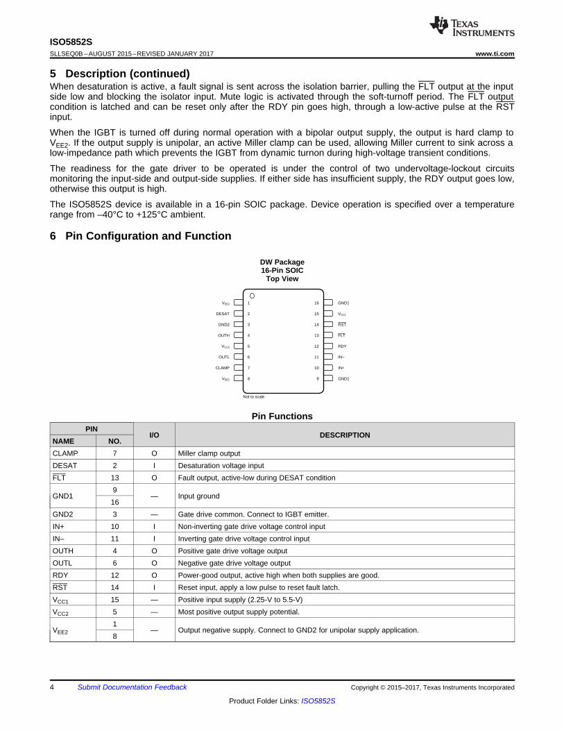
6 Pin Configuration and Function
DW Package16-Pin SOIC
Top View
Pin FunctionsPIN
I/O DESCRIPTIONNAME NO.CLAMP 7 O Miller clamp outputDESAT 2 I Desaturation voltage inputFLT 13 O Fault output, active-low during DESAT condition
GND19
— Input ground16
GND2 3 — Gate drive common. Connect to IGBT emitter.IN+ 10 I Non-inverting gate drive voltage control inputIN– 11 I Inverting gate drive voltage control inputOUTH 4 O Positive gate drive voltage outputOUTL 6 O Negative gate drive voltage outputRDY 12 O Power-good output, active high when both supplies are good.RST 14 I Reset input, apply a low pulse to reset fault latch.VCC1 15 — Positive input supply (2.25-V to 5.5-V)VCC2 5 — Most positive output supply potential.
VEE21
— Output negative supply. Connect to GND2 for unipolar supply application.8

5
ISO5852Swww.ti.com SLLSEQ0B –AUGUST 2015–REVISED JANUARY 2017
Product Folder Links: ISO5852S
Submit Documentation FeedbackCopyright © 2015–2017, Texas Instruments Incorporated
(1) Stresses beyond those listed under Absolute Maximum Ratings may cause permanent damage to the device. These are stress ratingsonly, which do not imply functional operation of the device at these or any other conditions beyond those indicated under RecommendedOperating Conditions. Exposure to absolute-maximum-rated conditions for extended periods may affect device reliability.
7 Specifications
7.1 Absolute Maximum RatingsOver operating free-air temperature range (unless otherwise noted) (1)
MIN MAX UNITVCC1 Supply-voltage input side GND1 – 0.3 6 VVCC2 Positive supply-voltage output side (VCC2 – GND2) –0.3 35 VVEE2 Negative supply-voltage output side (VEE2 – GND2) –17.5 0.3 VV(SUP2) Total-supply output voltage (VCC2 – VEE2) –0.3 35 VV(OUTH) Positive gate-driver output voltage VEE2 – 0.3 VCC2 + 0.3 VV(OUTL) Negative gate-driver output voltage VEE2 – 0.3 VCC2 + 0.3 V
I(OUTH) Gate-driver high output current Maximum pulse width = 10 μs, Maximumduty cycle = 0.2%) 2.7 A
I(OUTL) Gate-driver low output current Maximum pulse width = 10 μs, Maximumduty cycle = 0.2%) 5.5 A
V(LIP) Voltage at IN+, IN–,FLT, RDY, RST GND1 – 0.3 VCC1 + 0.3 VI(LOP) Output current of FLT, RDY 10 mAV(DESAT) Voltage at DESAT GND2 – 0.3 VCC2 + 0.3 VV(CLAMP) Clamp voltage VEE2 – 0.3 VCC2 + 0.3 VTJ Junction temperature –40 150 °CTSTG Storage temperature –65 150 °C
(1) JEDEC document JEP155 states that 500-V HBM allows safe manufacturing with a standard ESD control process.(2) JEDEC document JEP157 states that 250-V CDM allows safe manufacturing with a standard ESD control process.
7.2 ESD RatingsVALUE UNIT
V(ESD)Electrostaticdischarge
Human body model (HBM), per ANSI/ESDA/JEDEC JS-001 (1) ±4000V
Charged-device model (CDM), per JEDEC specification JESD22-C101 (2) ±1500
7.3 Recommended Operating Conditionsover operating free-air temperature range (unless otherwise noted)
MIN NOM MAX UNITVCC1 Supply-voltage input side 2.25 5.5 VVCC2 Positive supply-voltage output side (VCC2 – GND2) 15 30 VV(EE2) Negative supply-voltage output side (VEE2 – GND2) –15 0 VV(SUP2) Total supply-voltage output side (VCC2 – VEE2) 15 30 VV(IH) High-level input voltage (IN+, IN–, RST) 0.7 × VCC1 VCC1 VV(IL) Low-level input voltage (IN+, IN–, RST) 0 0.3 × VCC1 VtUI Pulse width at IN+, IN– for full output (CLOAD = 1 nF) 40 nstRST Pulse width at RST for resetting fault latch 800 nsTA Ambient temperature –40 125 °C
6
ISO5852SSLLSEQ0B –AUGUST 2015–REVISED JANUARY 2017 www.ti.com
Product Folder Links: ISO5852S
Submit Documentation Feedback Copyright © 2015–2017, Texas Instruments Incorporated
(1) For more information about traditional and new thermal metrics, see the Semiconductor and IC Package Thermal Metrics applicationreport.
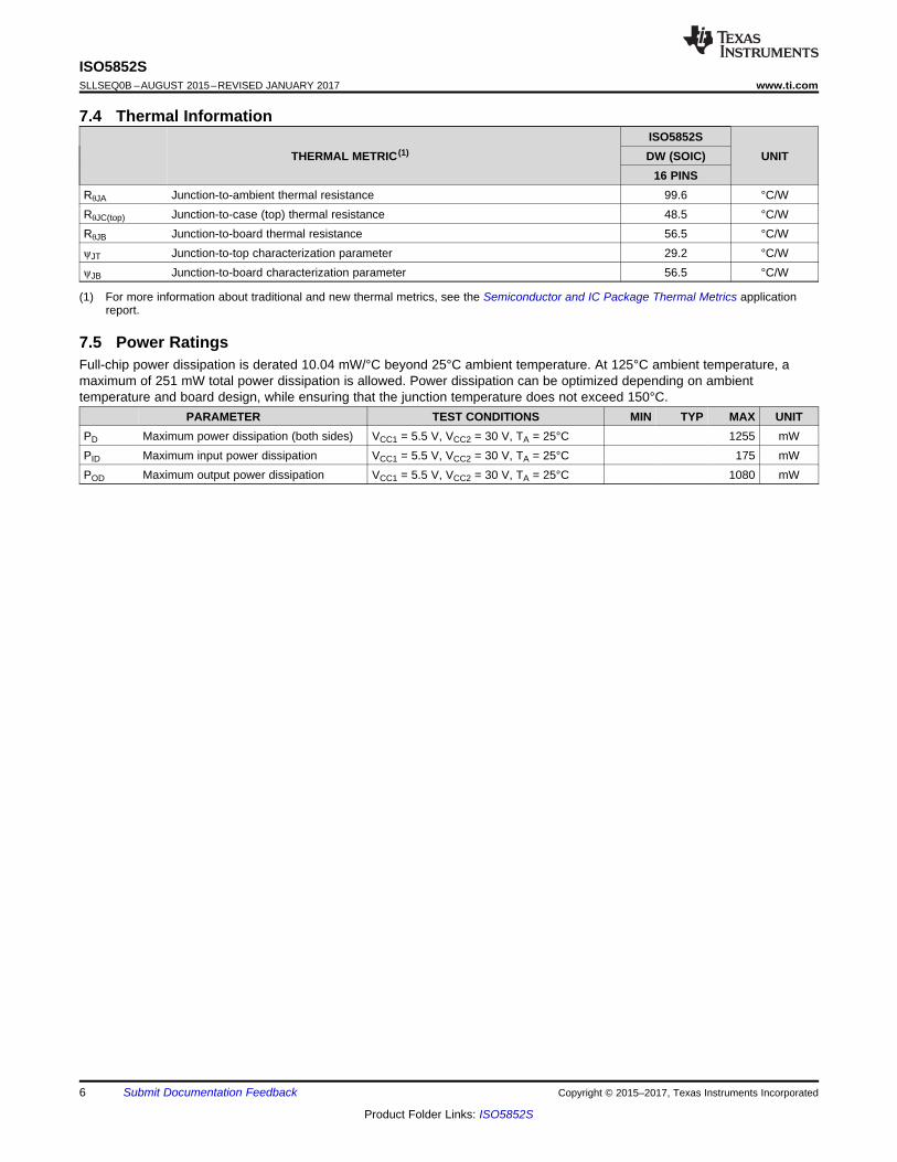
7.4 Thermal Information
THERMAL METRIC (1)ISO5852S
UNITDW (SOIC)16 PINS
RθJA Junction-to-ambient thermal resistance 99.6 °C/WRθJC(top) Junction-to-case (top) thermal resistance 48.5 °C/WRθJB Junction-to-board thermal resistance 56.5 °C/WψJT Junction-to-top characterization parameter 29.2 °C/WψJB Junction-to-board characterization parameter 56.5 °C/W
7.5 Power RatingsFull-chip power dissipation is derated 10.04 mW/°C beyond 25°C ambient temperature. At 125°C ambient temperature, amaximum of 251 mW total power dissipation is allowed. Power dissipation can be optimized depending on ambienttemperature and board design, while ensuring that the junction temperature does not exceed 150°C.
PARAMETER TEST CONDITIONS MIN TYP MAX UNITPD Maximum power dissipation (both sides) VCC1 = 5.5 V, VCC2 = 30 V, TA = 25°C 1255 mWPID Maximum input power dissipation VCC1 = 5.5 V, VCC2 = 30 V, TA = 25°C 175 mWPOD Maximum output power dissipation VCC1 = 5.5 V, VCC2 = 30 V, TA = 25°C 1080 mW

7
ISO5852Swww.ti.com SLLSEQ0B –AUGUST 2015–REVISED JANUARY 2017
Product Folder Links: ISO5852S
Submit Documentation FeedbackCopyright © 2015–2017, Texas Instruments Incorporated
(1) Creepage and clearance requirements should be applied according to the specific equipment isolation standards of an application. Careshould be taken to maintain the creepage and clearance distance of a board design to ensure that the mounting pads of the isolator onthe printed-circuit board do not reduce this distance. Creepage and clearance on a printed-circuit board become equal in certain cases.Techniques such as inserting grooves and/or ribs on a printed circuit board are used to help increase these specifications.
(2) This coupler is suitable for safe electrical insulation only within the maximum operating ratings. Compliance with the safety ratings shallbe ensured by means of suitable protective circuits.
(3) Testing is carried out in air or oil to determine the intrinsic surge immunity of the isolation barrier.(4) Apparent charge is electrical discharge caused by a partial discharge (pd).(5) All pins on each side of the barrier tied together creating a two-terminal device
7.6 Insulation SpecificationsPARAMETER TEST CONDITIONS VALUE UNIT
GENERALCLR External clearance (1) Shortest terminal-to-terminal distance through air 8 mm
CPG External creepage (1) Shortest terminal-to-terminal distance across thepackage surface 8 mm
DTI Distance through the insulation Minimum internal gap (internal clearance) 21 µm
CTI Comparative tracking index DIN EN 60112 (VDE 0303-11); IEC 60112;UL 746A >600 V
Material group According to IEC 60664-1 I
Overvoltage CategoryRated mains voltage ≤ 600 VRMS I-IVRated mains voltage ≤ 1000 VRMS I-III
DIN V VDE V 0884-10 (VDE V 0884-10):2006-12 (2)
VIORM Maximum repetitive peak isolation voltage AC voltage (bipolar) 2121 VPK
VIOWM Maximum isolation working voltageAC voltage (sine wave) Time dependent dielectricbreakdown (TDDB) test, see Figure 1 1500 VRMS
DC voltage 2121 VDC
VIOTM Maximum transient isolation voltage VTEST = VIOTM; t = 60 s (qualification); t = 1 s (100%production) 8000
VPKVIOSM Maximum surge isolation voltage (3) Test method per IEC 60065, 1.2/50 µs waveform,
VTEST = 1.6 × VIOSM = 12800 VPK (qualification) 8000
qpd Apparent charge (4)
Method a: After I/O safety test subgroup 2/3,Vini = VIOTM, tini = 60 s;Vpd(m) = 1.2 × VIORM = 2545 VPK ,tm = 10 s
≤5
pC
Method a: After environmental tests subgroup 1,Vini = VIOTM, tini = 60 s;Vpd(m) = 1.6 × VIORM = 3394 VPK ,tm = 10 s
≤5
Method b1: At routine test (100% production) andpreconditioning (type test)Vini = VIOTM, tini = 60 s;Vpd(m) = 1.875× VIORM = 3977 VPK ,tm = 10 s
≤5
CIO Barrier capacitance, input to output (5) VIO = 0.4 sin (2πft), f = 1 MHz ~1 pF
RIO Isolation resistance, input to output (5)
VIO = 500 V, TA = 25°C > 1012
ΩVIO = 500 V, 100°C ≤ TA ≤ 125°C > 1011
VIO = 500 V at TS = 150°C > 109
Pollution degree 2Climatic category 40/125/21
UL 1577
VISO Withstand isolation voltageVTEST = VISO = 5700 VRMS, t = 60 s (qualification);VTEST = 1.2 × VISO = 6840 VRMS, t = 1 s (100%production)
5700 VRMS

8
ISO5852SSLLSEQ0B –AUGUST 2015–REVISED JANUARY 2017 www.ti.com
Product Folder Links: ISO5852S
Submit Documentation Feedback Copyright © 2015–2017, Texas Instruments Incorporated
7.7 Safety-Related CertificationsVDE CSA UL CQC TUV
Certified according toDIN V VDE V 0884-10(VDE V 0884-10):2006-12 and DIN EN 61010-1(VDE 0411-1):2011-07
Certified according toCSA ComponentAcceptance Notice 5A,IEC 60950-1, and IEC60601-1
Recognized under UL1577 ComponentRecognition Program
Certified according toGB4943.1-2011
Certified according toEN 61010-1:2010 (3rd Ed) andEN 60950-1:2006/A11:2009/A1:2010/A12:2011/A2:2013
Reinforced InsulationMaximum Transientisolation voltage, 8000VPK;Maximum surge isolationvoltage, 8000 VPK,Maximum repetitive peakisolation voltage, 2121VPK
Isolation Rating of 5700VRMS;Reinforced insulationper CSA 60950-1-07+A1+A2 and IEC60950-1 (2nd Ed.), 800VRMS max workingvoltage (pollutiondegree 2, materialgroup I) ;2 MOPP (Means ofPatient Protection) perCSA 60601-1:14 andIEC 60601-1 Ed. 3.1,250 VRMS (354 VPK)max working voltage
Single Protection, 5700VRMS
Reinforced Insulation,Altitude ≤ 5000m, Tropicalclimate, 400 VRMSmaximum working voltage
5700 VRMS Reinforcedinsulation perEN 61010-1:2010 (3rd Ed) up toworking voltage of 600 VRMS5700 VRMS Reinforcedinsulation perEN 60950-1:2006/A11:2009/A1:2010/A12:2011/A2:2013 up toworking voltage of 800 VRMS
Certification completedCertificate number:40040142
Certification completedMaster contractnumber: 220991
Certification completedFile number: E181974
Certification completedCertificate number:CQC16001141761
Certification completedClient ID number: 77311
(1) Input, output, or the sum of input and output power should not exceed this value
7.8 Safety Limiting ValuesSafety limiting intends to minimize potential damage to the isolation barrier upon failure of input or output circuitry. A failure ofthe I/O can allow low resistance to ground or the supply and, without current limiting, dissipate sufficient power to overheatthe die and damage the isolation barrier, potentially leading to secondary system failures.
PARAMETER TEST CONDITIONS MIN TYP MAX UNIT
ISSafety input, output, or supplycurrent
RθJA = 99.6°C/W, VI = 2.75 V, TJ = 150°C, TA = 25°C,see Figure 2 456
mA
RθJA = 99.6°C/W, VI = 3.6 V, TJ = 150°C, TA = 25°C,see Figure 2 346
RθJA = 99.6°C/W, VI = 5.5 V, TJ = 150°C, TA = 25°C,see Figure 2 228
RθJA = 99.6°C/W, VI = 15 V, TJ = 150°C, TA = 25°C,see Figure 2 84
RθJA = 99.6°C/W, VI = 30 V, TJ = 150°C, TA = 25°C,see Figure 2 42
PSSafety input, output, or totalpower RθJA = 99.6°C/W, TJ = 150°C, TA = 25°C, see Figure 3 255 (1) mW
TSMaximum ambient safetytemperature 150 °C
The safety-limiting constraint is the maximum junction temperature specified in the data sheet. The powerdissipation and junction-to-air thermal impedance of the device installed in the application hardware determinesthe junction temperature. The assumed junction-to-air thermal resistance in the Thermal Information table is thatof a device installed on a high-K test board for leaded surface-mount packages. The power is the recommendedmaximum input voltage times the current. The junction temperature is then the ambient temperature plus thepower times the junction-to-air thermal resistance.

9
ISO5852Swww.ti.com SLLSEQ0B –AUGUST 2015–REVISED JANUARY 2017
Product Folder Links: ISO5852S
Submit Documentation FeedbackCopyright © 2015–2017, Texas Instruments Incorporated
(1) IIH for IN–, RST pin is zero as they are pulled high internally(2) IIL for IN+ is zero, as it is pulled low internally
7.9 Electrical CharacteristicsOver recommended operating conditions unless otherwise noted. All typical values are at TA = 25°C, VCC1 = 5 V, VCC2 –GND2 = 15 V, GND2 – VEE2 = 8 V
PARAMETER TEST CONDITIONS MIN TYP MAX UNIT
VOLTAGE SUPPLY
VIT+(UVLO1)Positive-going UVLO1 threshold-voltageinput side (VCC1 – GND1) 2.25 V
VIT-(UVLO1)Negative-going UVLO1 threshold-voltageinput side (VCC1 – GND1) 1.7 V
VHYS(UVLO1)UVLO1 Hysteresis voltage (VIT+ – VIT–)input side 0.2 V
VIT+(UVLO2)Positive-going UVLO2 threshold-voltageoutput side (VCC2 – GND2) 12 13 V
VIT–(UVLO2)Negative-going UVLO2 threshold-voltageoutput side (VCC2 – GND2) 9.5 11 V
VHYS(UVLO2)UVLO2 hysteresis voltage (VIT+ – VIT–)output side 1 V
IQ1 Input-supply quiescent current 2.8 4.5 mA
IQ2 Output-supply quiescent current 3.6 6 mA
LOGIC I/O
VIT+(IN,RST)Positive-going input-threshold voltage (IN+,IN–, RST) 0.7 × VCC1 V
VIT–(IN,RST)Negative-going input-threshold voltage(IN+, IN–, RST) 0.3 × VCC1 V
VHYS(IN,RST) Input hysteresis voltage (IN+, IN–, RST) 0.15 × VCC1 V
IIH High-level input leakage at (IN+) (1) IN+ = VCC1 100 µA
IIL Low-level input leakage at (IN–, RST) (2) IN– = GND1, RST = GND1 -100 µA
IPU Pullup current of FLT, RDY V(RDY) = GND1, V(FLT) = GND1 100 µA
V(OL) Low-level output voltage at FLT, RDY I(FLT) = 5 mA 0.2 V
GATE DRIVER STAGE
V(OUTPD) Active output pulldown voltage I(OUTH/L) = 200 mA, VCC2 = open 2 V
VOUTH High-level output voltage I(OUTH) = –20 mA VCC2 – 0.5 VCC2 – 0.24 V
VOUTL Low-level output voltage I(OUTL) = 20 mA VEE2 + 13 VEE2 + 50 mV
I(OUTH) High-level output peak current IN+ = high, IN– = low,V(OUTH) = VCC2 - 15 V 1.5 2.5 A
I(OUTL) Low-level output peak current IN+ = low, IN– = high,V(OUTL) = VEE2 + 15 V 3.4 5 A
I(OLF)Low-level output current during faultcondition 130 mA
ACTIVE MILLER CLAMP
V(CLP) Low-level clamp voltage I(CLP) = 20 mA VEE2 + 0.015 VEE2 + 0.08 V
I(CLP) Low-level clamp current V(CLAMP) = VEE2 + 2.5 V 1.6 2.5 3.3 A
V(CLTH) Clamp threshold voltage 1.6 2.1 2.5 V
SHORT CIRCUIT CLAMPING
V(CLP-OUTH)Clamping voltage(VOUTH – VCC2)
IN+ = high, IN– = low, tCLP = 10 µs,I(OUTH) = 500 mA 1.1 1.3 V
V(CLP-OUTL)Clamping voltage(VOUTL – VCC2)
IN+ = high, IN– = low, tCLP = 10 µs,I(OUTL) = 500 mA 1.3 1.5 V
V(CLP-CLP)Clamping voltage(VCLP – VCC2)
IN+ = high, IN– = low, tCLP = 10 µs,I(CLP) = 500 mA 1.3 V
V(CLP-CLAMP) Clamping voltage at CLAMP IN+ = High, IN– = Low,I(CLP) = 20 mA 0.7 1.1 V
V(CLP-OUTL)Clamping voltage at OUTL(VCLP – VCC2)
IN+ = High, IN– = Low,I(OUTL) = 20 mA 0.7 1.1 V
DESAT PROTECTION
I(CHG) Blanking-capacitor charge current V(DESAT) – GND2 = 2 V 0.42 0.5 0.58 mA
I(DCHG) Blanking-capacitor discharge current V(DESAT) – GND2 = 6 V 9 14 mA

10
ISO5852SSLLSEQ0B –AUGUST 2015–REVISED JANUARY 2017 www.ti.com
Product Folder Links: ISO5852S
Submit Documentation Feedback Copyright © 2015–2017, Texas Instruments Incorporated
Electrical Characteristics (continued)Over recommended operating conditions unless otherwise noted. All typical values are at TA = 25°C, VCC1 = 5 V, VCC2 –GND2 = 15 V, GND2 – VEE2 = 8 V
PARAMETER TEST CONDITIONS MIN TYP MAX UNIT
V(DSTH)DESAT threshold voltage with respect toGND2 8.3 9 9.5 V
V(DSL)DESAT voltage with respect to GND2,when OUTH or OUTL is driven low 0.4 1 V
(1) Measured at same supply voltage and temperature condition(2) Measured from input pin to ground.
7.10 Switching CharacteristicsOver recommended operating conditions unless otherwise noted. All typical values are at TA = 25°C, VCC1 = 5 V, VCC2 –GND2 = 15 V, GND2 – VEE2 = 8 V
PARAMETER TEST CONDITIONS MIN TYP MAX UNITtr Output-signal rise time at OUTH CLOAD = 1 nF
See Figure 44, Figure 45,and Figure 46
12 18 35 nstf Output-signal fall time at OUTL CLOAD = 1 nF 12 20 37 nstPLH, tPHL Propagation Delay CLOAD = 1 nF 76 110 nstsk-p Pulse skew |tPHL – tPLH| CLOAD = 1 nF 20 nstsk-pp Part-to-part skew CLOAD = 1 nF 30 (1) nstGF (IN,/RST) Glitch filter on IN+, IN–, RST CLOAD = 1 nF 20 30 40 nstDS (90%) DESAT sense to 90% VOUTH/L delay CLOAD = 10 nF 553 760 nstDS (10%) DESAT sense to 10% VOUTH/L delay CLOAD = 10 nF 2 3.5 μstDS (GF) DESAT-glitch filter delay CLOAD = 1 nF 330 nstDS (FLT) DESAT sense to FLT-low delay See Figure 46 1.4 μstLEB Leading-edge blanking time See Figure 44 and Figure 45 310 400 480 nstGF(RSTFLT) Glitch filter on RST for resetting FLT 300 800 ns
CI Input capacitance (2) VI = VCC1 / 2 + 0.4 × sin (2πft), f = 1 MHz,VCC1 = 5 V 2 pF
CMTI Common-mode transient immunity VCM = 1500 V, see Figure 47 100 120 kV/μs

Ambient Temperature (qC)
Saf
ety
Lim
iting
Pow
er (
mW
)
0 50 100 150 2000
200
400
600
800
1000
1200
1400Power
Stress Voltage (VRMS)
Tim
e to
Fai
l (s)
500 1500 2500 3500 4500 5500 6500 7500 8500 95001.E+1
1.E+2
1.E+3
1.E+4
1.E+5
1.E+6
1.E+7
1.E+8
1.E+9
1.E+10
1.E+11 Safety Margin Zone: 1800 VRMS, 254 YearsOperating Zone: 1500 VRMS, 135 Years
20%
87.5% TDDB Line (<1 PPM Fail Rate)
Ambient Temperature (qC)
Saf
ety
Lim
iting
Cur
rent
(m
A)
0 50 100 150 2000
50
100
150
200
250
300
350
400
450
500VCC1 = 2.75 VVCC1 = 3.6 VVCC1 = 5.5 VVCC2 = 15 VVCC2 = 30 V
11
ISO5852Swww.ti.com SLLSEQ0B –AUGUST 2015–REVISED JANUARY 2017
Product Folder Links: ISO5852S
Submit Documentation FeedbackCopyright © 2015–2017, Texas Instruments Incorporated
7.11 Insulation Characteristics Curves
TA up to 150°C Stress-voltage frequency = 60 Hz
Figure 1. Reinforced Isolation Capacitor Lifetime Projection Figure 2. Thermal Derating Curve for Limiting Current perVDE
Figure 3. Thermal Derating Curve for Limiting Power per VDE

Ambient Temperature (qC)
VD
ST
H -
DE
SA
T T
hres
hold
Vol
tage
(V
)
-40 -25 -10 5 20 35 50 65 80 95 110 1258.5
8.6
8.7
8.8
8.9
9
9.1
9.2
D005
15 V Unipolar30 V Unipolar
Ambient Temperature (qC)
I OL
- O
utpu
t Driv
e C
urre
nt (
A)
-40 -25 -10 5 20 35 50 65 80 95 110 1250
1
2
3
4
5
6
7
D002
VOUT - VEE2 = 2.5 VVOUT - VEE2 = 5 VVOUT - VEE2 = 10 V
VOUT - VEE2 = 15 VVOUT - VEE2 = 20 V
VOUTH/L - VEE2 Voltage (V)
I OL
- O
utpu
t Driv
e C
urre
nt (
A)
0 5 10 15 20 25 300
1
2
3
4
5
6
7
D004
TA = -40qCTA = 25qCTA = 125qC
Ambient Temperature (qC)
I OH -
Out
put D
rive
Cur
rent
(A
)
-40 -25 -10 5 20 35 50 65 80 95 110 125-4
-3.5
-3
-2.5
-2
-1.5
-1
-0.5
0
D001
VCC2 - VOUT = 2.5 VVCC2 - VOUT = 5 VVCC2 - VOUT = 10 V
VCC2 - VOUT = 15 VVCC2 - VOUT = 20 V
VCC2 - VOUTH/L Voltage (V)
I OH -
Out
put D
rive
Cur
rent
(A
)
0 5 10 15 20 25 30-4
-3.5
-3
-2.5
-2
-1.5
-1
-0.5
0
D003
TA = -40qCTA = 25qCTA = 125qC
12
ISO5852SSLLSEQ0B –AUGUST 2015–REVISED JANUARY 2017 www.ti.com
Product Folder Links: ISO5852S
Submit Documentation Feedback Copyright © 2015–2017, Texas Instruments Incorporated
7.12 Typical Characteristics
Figure 4. Output High Drive Current vs Temperature Figure 5. Output High Drive Current vs Output Voltage
Figure 6. Output Low Drive Current vs Temperature Figure 7. Output Low Drive Current vs Output Voltage
Unipolar: VCC2 – VEE2 = VCC2 – GND2
Figure 8. DESAT Threshold Voltage vs Temperature

2 s / Divm
CH
3:3
V/D
iv
500 ns / Div
CH
3:3
V/D
iv
2 s / Divm
CH
3:3 V
/Div
50 ns / Div
CH
3:3
V/D
iv
50 ns / Div
CH
3:3
V/D
iv
500 ns / Div
CH
3:3 V
/Div
13
ISO5852Swww.ti.com SLLSEQ0B –AUGUST 2015–REVISED JANUARY 2017
Product Folder Links: ISO5852S
Submit Documentation FeedbackCopyright © 2015–2017, Texas Instruments Incorporated
Typical Characteristics (continued)
CL = 1 nF RGH = 0 Ω RGL = 0 ΩVCC2 – VEE2 = VCC2 – GND2 = 20 V
Figure 9. Output Transient Waveform
CL = 10 nF RGH = 0 Ω RGL = 0 ΩVCC2 – VEE2 = VCC2 – GND2 = 20 V
Figure 10. Output Transient Waveform
CL = 100 nF RGH = 0 Ω RGL = 0 ΩVCC2 – VEE2 = VCC2 – GND2 = 20 V
Figure 11. Output Transient Waveform
CL = 1 nF RGH = 10 Ω RGL = 5 ΩVCC2 – VEE2 = VCC2 – GND2 = 20 V
Figure 12. Output Transient Waveform
CL = 10 nF RGH = 10 Ω RGL = 5 ΩVCC2 – VEE2 = VCC2 – GND2 = 20 V
Figure 13. Output Transient Waveform
CL = 100 nF RGH = 10 Ω RGL = 5 ΩVCC2 – VEE2 = VCC2 – GND2 = 20 V
Figure 14. Output Transient Waveform

Ambient Temperature (qC)
I CC
1 -
Sup
ply
Cur
rent
(m
A)
-40 -25 -10 5 20 35 50 65 80 95 110 1252
2.2
2.4
2.6
2.8
3
3.2
3.4
D006
VCC1 = 3 VVCC1 = 3.3 VVCC1 = 5 VVCC1 = 5.5 V
Ambient Temperature (qC)
I CC
1 -
Sup
ply
Cur
rent
(m
A)
-40 -25 -10 5 20 35 50 65 80 95 110 1251
1.1
1.2
1.3
1.4
1.5
1.6
1.7
1.8
1.9
2
D007
VCC1 = 3 VVCC1 = 3.3 VVCC1 = 5 VVCC1 = 5.5 V
1 s / Divm
CH
1:15 V
/Div
CH
3:5 V
/Div
CH
2:10 V
/Div
CH
4:5 V
/Div
OUT
DESAT
/FLT
RDY
2 s / Divm
CH
1:15 V
/Div
CH
3:5 V
/Div
CH
2:10 V
/Div
CH
4:5 V
/Div
OUT
DESAT
/FLT
RDY
1 µs/Div
CH
1:7.5
V/D
ivC
H 3
:5 V
/Div
CH
2:10 V
/Div
CH
4:5 V
/Div
OUT
DESAT
FLT
RDY
2 s / Divm
CH
1:7.5
V/D
ivC
H 3
:5 V
/Div
CH
2:10 V
/Div
CH
4:5 V
/Div
OUT
DESAT
/FLT
RDY
14
ISO5852SSLLSEQ0B –AUGUST 2015–REVISED JANUARY 2017 www.ti.com
Product Folder Links: ISO5852S
Submit Documentation Feedback Copyright © 2015–2017, Texas Instruments Incorporated
Typical Characteristics (continued)
CL = 10 nF RGH = 0 Ω RGL = 0 ΩVCC2 – VEE2 = VCC2 – GND2 = 15 V DESAT = 220 pF
Figure 15. Output Transient Waveform DESAT, RDY, andFLT
CL = 10 nF RGH = 0 Ω RGL = 0 ΩVCC2 – VEE2 = VCC2 – GND2 = 15 V DESAT = 220 pF
Figure 16. Output Transient Waveform DESAT, RDY, andFLT
CL = 10 nF RGH = 0 Ω RGL = 0 ΩVCC2 – VEE2 = VCC2 – GND2 = 30 V DESAT = 220 pF
Figure 17. Output Transient Waveform DESAT, RDY, andFLT
CL = 10 nF RGH = 0 Ω RGL = 0 ΩVCC2 – VEE2 = VCC2 – GND2 = 30 V DESAT = 220 pF
Figure 18. Output Transient Waveform DESAT, RDY, andFLT
IN+ = High IN– = Low
Figure 19. ICC1 Supply Current vs Temperature
IN+ = Low IN– = Low
Figure 20. ICC1 Supply Current vs Temperature

Ambient Temperature (qC)
Pro
paga
tion
Del
ay (
ns)
-40 -25 -10 5 20 35 50 65 80 95 110 1250
10
20
30
40
50
60
70
80
90
100
D012
tpLH at VCC2 = 15 VtpHL at VCC2 = 15 VtpLH at VCC2 = 30 VtpHL at VCC2 = 30 V
Ambient Temperature (qC)
Pro
paga
tion
Del
ay (
ns)
-40 -25 -10 5 20 35 50 65 80 95 110 1250
10
20
30
40
50
60
70
80
90
100
D013
tpLH at VCC1 = 3.3 VtpHL at VCC1 = 3.3 VtpLH at VCC1 = 5 VtpHL at VCC1 = 5 V
Input Frequency - (kHz)
I CC
2 -
Sup
ply
Cur
rent
(m
A)
0 50 100 150 200 250 3002
2.5
3
3.5
4
4.5
5
5.5
D009
VCC2 = 15 VVCC2 = 20 VVCC2 = 30 V
Load Capacitance (nF)
I CC
2 -
Sup
ply
Cur
rent
(m
A)
0 10 20 30 40 50 60 70 80 90 1000
10
20
30
40
50
60
70
D011
VCC2 = 15 VVCC2 = 30 V
Input Frequency - (kHz)
I CC
1 -
Sup
ply
Cur
rent
(m
A)
0 50 100 150 200 250 3000
0.5
1
1.5
2
2.5
3
D008
VCC1 = 3 VVCC1 = 5.5 V
Ambient Temperature (qC)
I CC
2 -
Sup
ply
Cur
rent
(m
A)
-40 -25 -10 5 20 35 50 65 80 95 110 1252
2.5
3
3.5
4
4.5
5
D010
VCC2 = 15 VVCC2 = 20 VVCC2 = 30 V
15
ISO5852Swww.ti.com SLLSEQ0B –AUGUST 2015–REVISED JANUARY 2017
Product Folder Links: ISO5852S
Submit Documentation FeedbackCopyright © 2015–2017, Texas Instruments Incorporated
Typical Characteristics (continued)
Figure 21. ICC1 Supply Current vs Input Frequency
Input frequency = 1 kHz
Figure 22. ICC2 Supply Current vs Temperature
No CL
Figure 23. ICC2 Supply Current vs Input Frequency
RGH = 10 Ω RGL = 5 Ω, 20 kHz
Figure 24. ICC2 Supply Current vs Load Capacitance
CL = 1 nF RGH = 0 Ω RGL = 0 ΩVCC1 = 5 V
Figure 25. Propagation Delay vs Temperature
CL = 1 nF RGH = 0 Ω RGL = 0 ΩVCC2 = 15 V
Figure 26. Propagation Delay vs Temperature

Load Capacitance (nF)
Tra
nsis
tion
Tim
e (n
s)
0 10 20 30 40 50 60 70 80 90 1000
200
400
600
800
1000
1200
1400
1600
1800
2000
D018
VCC2 = 15 VVCC2 = 30 V
Ambient Temperature (qC)
t LE
B -
Lea
ding
Edg
e B
lank
ing
Tim
e (n
s)
-40 -25 -10 5 20 35 50 65 80 95 110 125300
320
340
360
380
400
420
440
460
480
500
D019
VCC2 = 15 VVCC2 = 30 V
Load Capacitance (nF)
Tra
nsis
tion
Tim
e (n
s)
0 10 20 30 40 50 60 70 80 90 1000
100
200
300
400
500
600
D016
VCC2 = 15 VVCC2 = 30 V
Load Capacitance (nF)
Tra
nsis
tion
Tim
e (n
s)
0 10 20 30 40 50 60 70 80 90 1000
1000
2000
3000
4000
5000
6000
D017
VCC2 = 15 VVCC2 = 30 V
Ambient Temperature (qC)
Pro
paga
tion
Del
ay (
ns)
0 10 20 30 40 50 60 70 80 90 1000
200
400
600
800
1000
1200
D014
tpLH at VCC2 = 15 VtpLH at VCC2 = 30 VtpHL at VCC2 = 15 VtpHL at VCC2 = 30 V
Load Capacitance (nF)
Tra
nsis
tion
Tim
e (n
s)
0 10 20 30 40 50 60 70 80 90 1000
100
200
300
400
500
600
700
800
900
1000
D015
VCC2 = 15 VVCC2 = 30 V
16
ISO5852SSLLSEQ0B –AUGUST 2015–REVISED JANUARY 2017 www.ti.com
Product Folder Links: ISO5852S
Submit Documentation Feedback Copyright © 2015–2017, Texas Instruments Incorporated
Typical Characteristics (continued)
RGH = 10 Ω RGL = 5 Ω VCC1 = 5 V
Figure 27. Propagation Delay vs Load Capacitance
RGH = 0 Ω RGL = 0 Ω VCC1 = 5 V
Figure 28. tr Rise Time vs Load Capacitance
RGH = 0 Ω RGL = 0 Ω VCC1 = 5 V
Figure 29. tf Fall Time v. Load Capacitance
RGH = 10 Ω RGL = 5 Ω VCC1 = 5 V
Figure 30. tr Rise Time vs Load Capacitance
RGH = 10 Ω RGL = 5 Ω VCC1 = 5 V
Figure 31. tf Fall Time vs Load Capacitance Figure 32. Leading Edge Blanking Time With Temperature

Ambient Temperature (qC)
Res
et T
o F
ault
Del
ay (
ns)
-40 -25 -10 5 20 35 50 65 80 95 110 1250
20
40
60
80
100
120
D023
VCC1 = 3 VVCC1 = 3.3 VVCC1 = 5 VVCC1 = 5.5 V
Ambient Temperature (qC)
I CLP
- C
lam
p Lo
w-L
evel
Cur
rent
(A
)
-40 -25 -10 5 20 35 50 65 80 95 110 1250
0.5
1
1.5
2
2.5
3
3.5
4
4.5
5
D025
V(CLAMP) = 2 VV(CLAMP) = 4 VV(CLAMP) = 6 V
Ambient Temperature (qC)
t DE
SA
T(/
FLT
) -
DE
SA
T S
ense
to /F
LT L
ow D
elay
(P
s)
-40 -25 -10 5 20 35 50 65 80 95 110 1251.05
1.10
1.15
1.20
1.25
D022
VCC2 = 15 VVCC2 = 30 V
Ambient Temperature (qC)
/FLT
and
RD
Y L
ow to
RD
Y H
igh
Del
ay (P
s)
-40 -25 -10 5 20 35 50 65 80 95 110 1253.4
3.6
3.8
4
4.2
4.4
4.6
4.8
5
D024
VCC1 = 5 V, VCC2 = 15 V
Ambient Temperature (qC)
t DE
SA
T(1
0%) -
DE
SA
T S
ense
to 1
0% V
OU
T D
elay
(P
s)
-40 -25 -10 5 20 35 50 65 80 95 110 1251
1.5
2
2.5
3
3.5
4
D020
VCC2 = 15 VVCC2 = 30 V
Ambient Temperature (qC)
t DE
SA
T(9
0%) -
DE
SA
T S
ense
to 9
0% V
OU
T D
elay
(P
s)
-40 -25 -10 5 20 35 50 65 80 95 110 125450
470
490
510
530
550
570
590
610
D021
VCC2 = 15 VVCC2 = 30 V
17
ISO5852Swww.ti.com SLLSEQ0B –AUGUST 2015–REVISED JANUARY 2017
Product Folder Links: ISO5852S
Submit Documentation FeedbackCopyright © 2015–2017, Texas Instruments Incorporated
Typical Characteristics (continued)
CL = 10 nF RGH = 0 Ω RGL = 0 Ω
Figure 33. DESAT Sense to VOUT 10% Delay vs Temperature
CL = 10 nF RGH = 0 Ω RGL = 0 Ω
Figure 34. DESAT Sense to VOUT 90% Delay vs Temperature
Figure 35. DESAT Sense to Fault Low Delay vs TemperatureFigure 36. Fault and RDY Low to RDY High Delay vs
Temperature
Figure 37. Reset to Fault Delay Across Temperature Figure 38. Miller Clamp Current vs Temperature

Ambient Temperature (qC)
I CH
G -
Bla
nkin
g C
apac
itor
Cha
rgin
g C
urre
nt -
(P
A)
-40 -25 -10 5 20 35 50 65 80 95 110 125-600
-580
-560
-540
-520
-500
-480
-460
-440
-420
-400
D030
VDESAT = 6 V
Ambient Temperature (Cq)
VO
UT
H_C
LAM
P S
hort
Circ
uit C
lam
p V
olta
ge o
n O
UT
Acr
oss
Tem
pera
ture
-40 -20 0 20 40 60 80 100 120 1400.0
200.0
400.0
600.0
800.0
1000.0
1200.0
1400.0
D027
20mA at VCC2 = 15V20mA at VCC2 = 30V250mA at VCC2 = 15V
250mA at VCC2 = 30V500mA at VCC2 = 15V500mA at VCC2 = 30V
Ambient Temperature (Cq)
VO
UT
L_C
LAM
P S
hort
Circ
uit C
lam
p V
olta
ge o
n O
UT
Acr
oss
Tem
pera
ture
-40 -20 0 20 40 60 80 100 120 1400
200
400
600
800
1000
1200
1400
D028
20mA at VCC2 = 15V20mA at VCC2 = 30V250mA at VCC2 = 15V
250mA at VCC2 = 30V500mA at VCC2 = 15V500mA at VCC2 = 30V
Ambient Temperature (qC)
Act
ive
Pul
l Dow
n V
olta
ge (
V)
-40 -25 -10 5 20 35 50 65 80 95 110 1250
0.2
0.4
0.6
0.8
1
1.2
1.4
1.6
1.8
2
D026
I(OUTH/L) = 100 mAI(OUTH/L) = 200 mA
Ambient Temperature (Cq)
VC
LP_C
LAM
P S
hort
Circ
uit C
lam
p V
olta
ge o
n C
lam
p A
cros
s T
empe
ratu
re
-40 -20 0 20 40 60 80 100 120 1400
200
400
600
800
1000
1200
1400
D029
20mA at VCC2 = 15V20mA at VCC2 = 30V250mA at VCC2 = 15V
250mA at VCC2 = 30V500mA at VCC2 = 15V500mA at VCC2 = 30V
18
ISO5852SSLLSEQ0B –AUGUST 2015–REVISED JANUARY 2017 www.ti.com
Product Folder Links: ISO5852S
Submit Documentation Feedback Copyright © 2015–2017, Texas Instruments Incorporated
Typical Characteristics (continued)
Figure 39. Active Pulldown Voltage vs Temperature Figure 40. VCLP_CLAMP - Short-Circuit Clamp Voltage onClamp Across Temperature
Figure 41. VOUTH_CLAMP - Short-Circuit Clamp Voltage onOUTH Across Temperature
Figure 42. VOUTL_CLAMP - Short-Circuit Clamp Voltage onOUTL Across Temperature
VCC2 = 15 V DESAT = 6 V
Figure 43. Blanking Capacitor Charging Current vs Temperature
IN±
50 % 50 %
tftr
tPLH tPHL
90%
50%
10%OUTH/L
VCC1IN+
IN+50 % 50 %
tftr
tPLH tPHL
90%
50%
10%OUTH/L
0 VIN±
19
ISO5852Swww.ti.com SLLSEQ0B –AUGUST 2015–REVISED JANUARY 2017
Product Folder Links: ISO5852S
Submit Documentation FeedbackCopyright © 2015–2017, Texas Instruments Incorporated
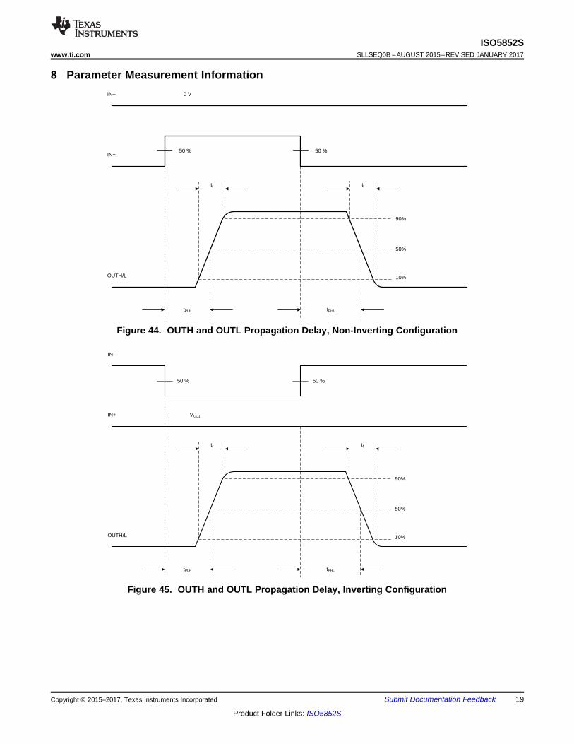
8 Parameter Measurement Information
Figure 44. OUTH and OUTL Propagation Delay, Non-Inverting Configuration
Figure 45. OUTH and OUTL Propagation Delay, Inverting Configuration

OUTL
DESAT
GND2
OUTH
15V1µF
VEE2
CLAMP
3
1, 8
5
4
6
2
7
15
9 , 16
11
10
12
13
14
IN -
IN+
RDY
VCC1
0.1µF
GND1
1nF
Iso
lati
on
Ba
rrie
r
+
-
Pass ± Fail Criterion :OUT must remain stable
CL
S1
+
-
VCM+ -
FLT
RST
VCC2
2.25 V- 5.5 V
Copyright © 2016, Texas Instruments Incorporated
tMute
tRST
RST-rising edge turns FLT high
tDS(FLT)
tLEB
VDSTH
tDS(10%)
10%
90%
tDS(90%)
Inputs blocked
Inputs released
IN+(IN± = GND1)
VOUTH/L
DESAT
FLT
RST
RDY
The inputs are muted for 5 µs by internal circuit after DESAT is detected. RDY is also low until the mute time.
FLT can be reset, only if RDY goes high.
20
ISO5852SSLLSEQ0B –AUGUST 2015–REVISED JANUARY 2017 www.ti.com
Product Folder Links: ISO5852S
Submit Documentation Feedback Copyright © 2015–2017, Texas Instruments Incorporated
Parameter Measurement Information (continued)
Figure 46. DESAT, OUTH/L, FLT, RST Delay
Figure 47. Common-Mode Transient Immunity Test Circuit

GND1 VEE2
RST
RDY
FLT
IN+
IN±
VCC1 VCC2
DESAT
GND2
OUTH
OUTL
CLAMP
VCC1
VCC1
UVLO1
Mute
DecoderQ S
RQ
VCC1
VCC1
Gate Drive
and
Encoder Logic
UVLO2
2 V
9 V
500 µA
STO
VCC2
Ready
Fault
Copyright © 2016, Texas Instruments Incorporated
21
ISO5852Swww.ti.com SLLSEQ0B –AUGUST 2015–REVISED JANUARY 2017
Product Folder Links: ISO5852S
Submit Documentation FeedbackCopyright © 2015–2017, Texas Instruments Incorporated
9 Detailed Description
9.1 OverviewThe ISO5852S is an isolated gate driver for IGBTs and MOSFETs. Input CMOS logic and output power stageare separated by a Silicon dioxide (SiO2) capacitive isolation.
The IO circuitry on the input side interfaces with a micro controller and consists of gate drive control and RESET(RST) inputs, READY (RDY) and FAULT (FLT) alarm outputs. The power stage consists of power transistors tosupply 2.5-A pullup and 5-A pulldown currents to drive the capacitive load of the external power transistors, aswell as DESAT detection circuitry to monitor IGBT collector-emitter overvoltage under short circuit events. Thecapacitive isolation core consists of transmit circuitry to couple signals across the capacitive isolation barrier, andreceive circuitry to convert the resulting low-swing signals into CMOS levels. The ISO5852S also contains undervoltage lockout circuitry to prevent insufficient gate drive to the external IGBT, and active output pulldown featurewhich ensures that the gate-driver output is held low, if the output supply voltage is absent. The ISO5852S alsohas an active Miller clamp function which can be used to prevent parasitic turn-on of the external powertransistor, due to Miller effect, for unipolar supply operation.
9.2 Functional Block Diagram
22
ISO5852SSLLSEQ0B –AUGUST 2015–REVISED JANUARY 2017 www.ti.com
Product Folder Links: ISO5852S
Submit Documentation Feedback Copyright © 2015–2017, Texas Instruments Incorporated
9.3 Feature Description
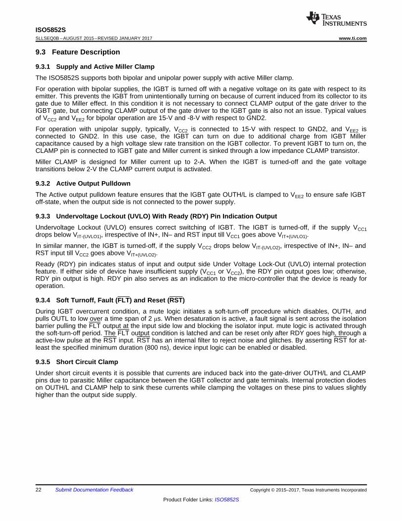
9.3.1 Supply and Active Miller ClampThe ISO5852S supports both bipolar and unipolar power supply with active Miller clamp.
For operation with bipolar supplies, the IGBT is turned off with a negative voltage on its gate with respect to itsemitter. This prevents the IGBT from unintentionally turning on because of current induced from its collector to itsgate due to Miller effect. In this condition it is not necessary to connect CLAMP output of the gate driver to theIGBT gate, but connecting CLAMP output of the gate driver to the IGBT gate is also not an issue. Typical valuesof VCC2 and VEE2 for bipolar operation are 15-V and -8-V with respect to GND2.
For operation with unipolar supply, typically, VCC2 is connected to 15-V with respect to GND2, and VEE2 isconnected to GND2. In this use case, the IGBT can turn on due to additional charge from IGBT Millercapacitance caused by a high voltage slew rate transition on the IGBT collector. To prevent IGBT to turn on, theCLAMP pin is connected to IGBT gate and Miller current is sinked through a low impedance CLAMP transistor.
Miller CLAMP is designed for Miller current up to 2-A. When the IGBT is turned-off and the gate voltagetransitions below 2-V the CLAMP current output is activated.
9.3.2 Active Output PulldownThe Active output pulldown feature ensures that the IGBT gate OUTH/L is clamped to VEE2 to ensure safe IGBToff-state, when the output side is not connected to the power supply.
9.3.3 Undervoltage Lockout (UVLO) With Ready (RDY) Pin Indication OutputUndervoltage Lockout (UVLO) ensures correct switching of IGBT. The IGBT is turned-off, if the supply VCC1drops below VIT-(UVLO1), irrespective of IN+, IN– and RST input till VCC1 goes above VIT+(UVLO1).
In similar manner, the IGBT is turned-off, if the supply VCC2 drops below VIT-(UVLO2), irrespective of IN+, IN– andRST input till VCC2 goes above VIT+(UVLO2).
Ready (RDY) pin indicates status of input and output side Under Voltage Lock-Out (UVLO) internal protectionfeature. If either side of device have insufficient supply (VCC1 or VCC2), the RDY pin output goes low; otherwise,RDY pin output is high. RDY pin also serves as an indication to the micro-controller that the device is ready foroperation.
9.3.4 Soft Turnoff, Fault (FLT) and Reset (RST)During IGBT overcurrent condition, a mute logic initiates a soft-turn-off procedure which disables, OUTH, andpulls OUTL to low over a time span of 2 μs. When desaturation is active, a fault signal is sent across the isolationbarrier pulling the FLT output at the input side low and blocking the isolator input. mute logic is activated throughthe soft-turn-off period. The FLT output condition is latched and can be reset only after RDY goes high, through aactive-low pulse at the RST input. RST has an internal filter to reject noise and glitches. By asserting RST for at-least the specified minimum duration (800 ns), device input logic can be enabled or disabled.
9.3.5 Short Circuit ClampUnder short circuit events it is possible that currents are induced back into the gate-driver OUTH/L and CLAMPpins due to parasitic Miller capacitance between the IGBT collector and gate terminals. Internal protection diodeson OUTH/L and CLAMP help to sink these currents while clamping the voltages on these pins to values slightlyhigher than the output side supply.

23
ISO5852Swww.ti.com SLLSEQ0B –AUGUST 2015–REVISED JANUARY 2017
Product Folder Links: ISO5852S
Submit Documentation FeedbackCopyright © 2015–2017, Texas Instruments Incorporated
(1) PU: Power Up (VCC1 ≥ 2.25 V, VCC2 ≥ 13 V), PD: Power Down (VCC1 ≤ 1.7 V, VCC2 ≤ 9.5 V), X: Irrelevant
9.4 Device Functional ModesIn ISO5852S OUTH/L to follow IN+ in normal functional mode, FLT pin must be in the high state. Table 1 lists thedevice functions.
Table 1. Function Table (1)
VCC1 VCC2 IN+ IN– RST RDY OUTH/L
PU PD X X X Low Low
PD PU X X X Low Low
PU PU X X Low High Low
PU Open X X X Low Low
PU PU Low X X High Low
PU PU X High X High Low
PU PU High Low High High High

24
ISO5852SSLLSEQ0B –AUGUST 2015–REVISED JANUARY 2017 www.ti.com
Product Folder Links: ISO5852S
Submit Documentation Feedback Copyright © 2015–2017, Texas Instruments Incorporated
10 Application and Implementation
NOTEInformation in the following applications sections is not part of the TI componentspecification, and TI does not warrant its accuracy or completeness. TI’s customers areresponsible for determining suitability of components for their purposes. Customers shouldvalidate and test their design implementation to confirm system functionality.
10.1 Application InformationThe ISO5852S device is an isolated gate driver for power semiconductor devices such as IGBTs and MOSFETs.It is intended for use in applications such as motor control, industrial inverters and switched mode powersupplies. In these applications, sophisticated PWM control signals are required to turn the power devices on andoff, which at the system level eventually may determine, for example, the speed, position, and torque of themotor or the output voltage, frequency and phase of the inverter. These control signals are usually the outputs ofa microcontroller, and are at low voltage levels such as 2.5 V, 3.3 V or 5 V. The gate controls required by theMOSFETs and IGBTs, however, are in the range of 30-V (using unipolar output supply) to 15-V (using bipolaroutput supply), and require high-current capability to drive the large capacitive loads offered by those powertransistors. The gate drive must also be applied with reference to the emitter of the IGBT (source for MOSFET),and by construction, the emitter node in a gate-drive system may swing between 0 to the DC-bus voltage, whichcan be several 100s of volts in magnitude.
The ISO5852S device is therefore used to level shift the incoming 2.5-V, 3.3-V, and 5-V control signals from themicrocontroller to the 30-V (using unipolar output supply) to 15-V (using bipolar output supply) drive required bythe power transistors while ensuring high-voltage isolation between the driver side and the microcontroller side.
10.2 Typical ApplicationsFigure 48 shows the typical application of a three-phase inverter using six ISO5852S isolated gate drivers.Three-phase inverters are used for variable-frequency drives to control the operating speed and torque of ACmotors and for high-power applications such as high-voltage DC (HVDC) power transmission.
The basic three-phase inverter consists of six power switches, and each switch is driven by one SO5852S. Theswitches are driven on and off at high switching frequency with specific patterns that to converter dc bus voltageto three-phase AC voltages.

µCM
ISO 5852S
ISO 5852S
ISO 5852S
ISO 5852S
ISO 5852S
ISO 5852S
3-Phase Input
PWM
123456
FAULT
25
ISO5852Swww.ti.com SLLSEQ0B –AUGUST 2015–REVISED JANUARY 2017
Product Folder Links: ISO5852S
Submit Documentation FeedbackCopyright © 2015–2017, Texas Instruments Incorporated
Typical Applications (continued)
Figure 48. Typical Motor-Drive Application
10.2.1 Design RequirementsUnlike optocoupler-based gate drivers which required external current drivers and biasing circuitry to provide theinput control signals, the input control to the device is CMOS and can be directly driven by the microcontroller.Other design requirements include decoupling capacitors on the input and output supplies, a pullup resistor onthe common-drain FLT output signal and RST input signal, and a high-voltage protection diode between theIGBT collector and the DESAT input. Further details are explained in the subsequent sections. Table 2 lists theallowed range for input and output supply voltage, and the typical current output available from the gate-driver.
Table 2. Design ParametersPARAMETER VALUE
Input supply voltage 2.25 V to 5.5 VUnipolar output-supply voltage (VCC2 – GND2 = VCC2 – VEE2) 15 V to 30 V
Bipolar output-supply voltage (VCC2 – VEE2) 15 V to 30 VBipolar output-supply voltage (GND2 – VEE2) 0 V to 15 V
Output current 2.5 A
10.2.2 Detailed Design Procedure
10.2.2.1 Recommended ISO5852S Application CircuitThe ISO5852S device has both, inverting and noninverting gate-control inputs, an active-low reset input, and anopen-drain fault output suitable for wired-OR applications. The recommended application circuit in Figure 49shows a typical gate-driver implementation with unipolar output supply. Figure 50 shows a typical gate-driverimplementation with bipolar output supply using the ISO5852S device.

ISO5852S15
916
11
10
12
13
14
IN±
IN+
RDY
RST
VCC1
GND1
2.25 to 5 V
FLT
10
+
± 0.1 µF
10 k 10 k
µC
Copyright © 2016, Texas Instruments Incorporated
DESAT
GND2
VCC2
OUTH
15 V
ISO5852S
DDST
VEE2
CLAMP
OUTL
3
18
5
4
6
2
7
15
916
11
10
12
13
14
IN±
IN+
RDY
RST
VCC1
GND1
2.25 to 5 V
FLT
10
+
± 0.1 µF
10 k 10 k
+
±
+
±0.1 µF
1 k
220 pF
RGL
RGH
Copyright © 2016, Texas Instruments Incorporated
DESAT
GND2
VCC2
OUTH
15 V
ISO5852S
DDST
VEE2
CLAMP
OUTL
3
18
5
4
6
2
7
15 V
15
916
11
10
12
13
14
IN±
IN+
RDY
RST
VCC1
GND1
2.25 to 5 V
FLT
10
+
± 0.1 µF
10 k 10 k
+
±
+
±
+
±0.1 µF
0.1 µF
1 k
220 pF
RGL
RGH
Copyright © 2016, Texas Instruments Incorporated
26
ISO5852SSLLSEQ0B –AUGUST 2015–REVISED JANUARY 2017 www.ti.com
Product Folder Links: ISO5852S
Submit Documentation Feedback Copyright © 2015–2017, Texas Instruments Incorporated
A 0.1-μF bypass capacitor, recommended at the input supply pin VCC1, and 1-μF bypass capacitor,recommended at the VCC2 output supply pin, provide the large transient currents required during a switchingtransition to ensure reliable operation. The 220-pF blanking capacitor disables DESAT detection during the off-to-on transition of the power device. The DESAT diode (DDST) and the 1-kΩ series resistor on the DESAT pin areexternal protection components. The RG gate resistor limits the gate-charge current and indirectly controls therise and fall times of the IGBT collector voltage. The open-drain FLT output and RDY output have a passive10-kΩ pullup resistor. In this application, the IGBT gate driver is disabled when a fault is detected and does notresume switching until the microcontroller applies a reset signal.
Figure 49. Unipolar Output Supply Figure 50. Bipolar Output Supply
10.2.2.2 FLT and RDY Pin CircuitryA is 50-kΩ pullup resistor exists internally on FLT and RDY pins. The FLT and RDY pins are an open-drainoutput. A 10-kΩ pullup resistor can be used to make it faster rise and to provide logic high when FLT and RDY isinactive, as shown in Figure 51.
Fast common-mode transients can inject noise and glitches on FLT and RDY pins because of parasitic coupling.The injection of noise and glitches is dependent on board layout. If required, additional capacitance (100 pF to300 pF) can be included on the FLT and RDY pins.
Figure 51. FLT and RDY Pin Circuitry for High CMTI
ISO5852S15
916
11
10
12
13
14
IN±
IN+
RDY
RST
VCC1
GND1
2.25 to 5 V
FLT
10
+
± 0.1 µF
10 k 10 k
µC
ISO5852S15
916
11
10
12
13
14
IN±
IN+
RDY
RST
VCC1
GND1
2.25 to 5 V
FLT
10
+
± 0.1 µF
10 k 10 k
µC
Copyright © 2016, Texas Instruments Incorporated
27
ISO5852Swww.ti.com SLLSEQ0B –AUGUST 2015–REVISED JANUARY 2017
Product Folder Links: ISO5852S
Submit Documentation FeedbackCopyright © 2015–2017, Texas Instruments Incorporated
10.2.2.3 Driving the Control InputsThe amount of common-mode transient immunity (CMTI) can be curtailed by the capacitive coupling from thehigh-voltage output circuit to the low-voltage input side of the ISO5852S device. For maximum CMTIperformance, the digital control inputs, IN+ and IN–, must be actively driven by standard CMOS, push-pull drivecircuits. This type of low-impedance signal source provides active drive signals that prevent unwanted switchingof the ISO5852S output under extreme common-mode transient conditions. Passive drive circuits, such as open-drain configurations using pullup resistors, must be avoided. A 20-ns glitch filter exists that can filter a glitch up to20 ns on IN+ or IN–.
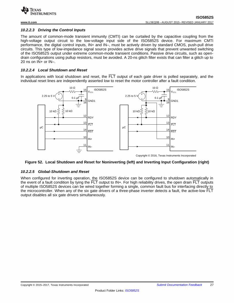
10.2.2.4 Local Shutdown and ResetIn applications with local shutdown and reset, the FLT output of each gate driver is polled separately, and theindividual reset lines are independently asserted low to reset the motor controller after a fault condition.
Figure 52. Local Shutdown and Reset for Noninverting (left) and Inverting Input Configuration (right)
10.2.2.5 Global-Shutdown and ResetWhen configured for inverting operation, the ISO5852S device can be configured to shutdown automatically inthe event of a fault condition by tying the FLT output to IN+. For high reliability drives, the open drain FLT outputsof multiple ISO5852S devices can be wired together forming a single, common fault bus for interfacing directly tothe microcontroller. When any of the six gate drivers of a three-phase inverter detects a fault, the active-low FLToutput disables all six gate drivers simultaneously.
ISO5852S15
916
11
10
12
13
14
IN±
IN+
RDY
RST
VCC1
GND1
2.25 to 5 V
FLT
10
+
± 0.1 µF
10 k 10 k
µC
ISO5852S15
916
11
10
12
13
14
IN±
IN+
RDY
RST
VCC1
GND1
2.25 to 5 V
FLT
10
+
± 0.1 µF
10 k 10 k
µC
Copyright © 2016, Texas Instruments Incorporated
ISO5852S15
916
11
10
12
13
14
IN±
IN+
RDY
RST
VCC1
GND1
2.25 to 5 V
FLT
10
+
± 0.1 µF
10 k 10 k
µC
To otherFLT pins
To otherRST pins
Copyright © 2016, Texas Instruments Incorporated
28
ISO5852SSLLSEQ0B –AUGUST 2015–REVISED JANUARY 2017 www.ti.com
Product Folder Links: ISO5852S
Submit Documentation Feedback Copyright © 2015–2017, Texas Instruments Incorporated
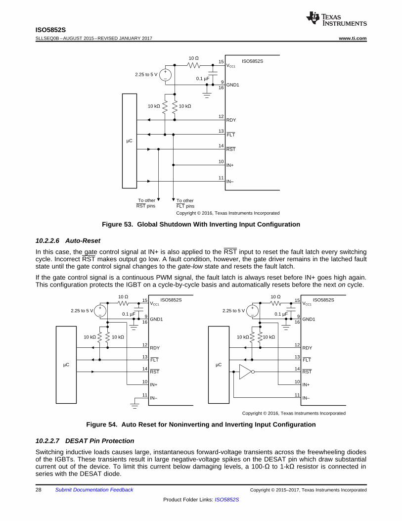
Figure 53. Global Shutdown With Inverting Input Configuration
10.2.2.6 Auto-ResetIn this case, the gate control signal at IN+ is also applied to the RST input to reset the fault latch every switchingcycle. Incorrect RST makes output go low. A fault condition, however, the gate driver remains in the latched faultstate until the gate control signal changes to the gate-low state and resets the fault latch.
If the gate control signal is a continuous PWM signal, the fault latch is always reset before IN+ goes high again.This configuration protects the IGBT on a cycle-by-cycle basis and automatically resets before the next on cycle.
Figure 54. Auto Reset for Noninverting and Inverting Input Configuration
10.2.2.7 DESAT Pin ProtectionSwitching inductive loads causes large, instantaneous forward-voltage transients across the freewheeling diodesof the IGBTs. These transients result in large negative-voltage spikes on the DESAT pin which draw substantialcurrent out of the device. To limit this current below damaging levels, a 100-Ω to 1-kΩ resistor is connected inseries with the DESAT diode.

DESAT
GND2
VCC2
OUTH
15 V
ISO5852S
DDST
VEE2
CLAMP
OUTL
3
18
5
4
6
2
7
15 V
+
±
+
±0.1 µF
1 µF
RS
220 pF
RGL
RGH
VFW
VFW-Inst
+
±
Copyright © 2016, Texas Instruments Incorporated
29
ISO5852Swww.ti.com SLLSEQ0B –AUGUST 2015–REVISED JANUARY 2017
Product Folder Links: ISO5852S
Submit Documentation FeedbackCopyright © 2015–2017, Texas Instruments Incorporated
Further protection is possible through an optional Schottky diode, whose low-forward voltage assures clamping ofthe DESAT input to GND2 potential at low-voltage levels.
Figure 55. DESAT Pin Protection With Series Resistor and Schottky Diode
10.2.2.8 DESAT Diode and DESAT ThresholdThe function of the DESAT diode is to conduct forward current, allowing sensing of the saturated collector-to-emitter voltage of the IGBT, V(DESAT), (when the IGBT is on), and to block high voltages (when the IGBT is off).During the short transition time when the IGBT is switching, a commonly high dVCE/dt voltage ramp rate occursacross the IGBT. This ramp rate results in a charging current I(CHARGE) = C(D-DESAT) × dVCE/dt, charging theblanking capacitor. C(D-DESAT) is the diode capacitance at DESAT.
To minimize this current and avoid false DESAT triggering, fast switching diodes with low capacitance arerecommended. As the diode capacitance builds a voltage divider with the blanking capacitor, large collectorvoltage transients appear at DESAT attenuated by the ratio of 1+ C(BLANK) / C(D-DESAT).
Because the sum of the DESAT diode forward-voltage and the IGBT collector-emitter voltage make up thevoltage at the DESAT-pin, VF + VCE = V(DESAT), the VCE level, which triggers a fault condition, can be modified byadding multiple DESAT diodes in series: VCE-FAULT(TH) = 9 V – n × VF (where n is the number of DESAT diodes).
When using two diodes instead of one, diodes with half the required maximum reverse-voltage rating can beselected.
10.2.2.9 Determining the Maximum Available, Dynamic Output Power, POD-max
The ISO5852S maximum-allowed total power consumption of PD = 251 mW consists of the total input power, PID,the total output power, POD, and the output power under load, POL:
PD = PID + POD + POL (1)
With:PID = VCC1-max × ICC1-max = 5.5 V × 4.5 mA = 24.75 mW (2)
and:POD = (VCC2 – VEE2) × ICC2-max = (15 V – [–8 V]) × 6 mA = 138 mW (3)
then:POL = PD – PID – POD = 251 mW – 24.75 mW – 138 mW = 88.25 mW (4)
In comparison to POL, the actual dynamic output power under worst case condition, POL-WC, depends on a varietyof parameters:

( )OL-WC
4 Ω 2.5 ΩP = 0.5 20 kHz 650 nC 15 V ( 8 V) + = 72.61 mW
4 Ω + 10 Ω 2.5 Ω + 10 Ω
æ ö´ ´ ´ - - ´ç ÷
è ø
OUTH/L
VCC2
15 V
ISO5852S
VEE2
8 V
+
±Ron-max
Roff-max +
±
RG
QG
Copyright © 2016, Texas Instruments Incorporated
( ) on-max off-maxOL-WC INP G CC2 EE2
on-max G off-max G
r rP = 0.5 f Q V V +
r + R r + R
æ ö´ ´ ´ - ´ ç ÷
è ø
30
ISO5852SSLLSEQ0B –AUGUST 2015–REVISED JANUARY 2017 www.ti.com
Product Folder Links: ISO5852S
Submit Documentation Feedback Copyright © 2015–2017, Texas Instruments Incorporated
where• fINP = signal frequency at the control input IN+• QG = power device gate charge• VCC2 = positive output supply with respect to GND2• VEE2 = negative output supply with respect to GND2• ron-max = worst case output resistance in the on-state: 4 Ω• roff-max = worst case output resistance in the off-state: 2.5 Ω• RG = gate resistor (5)
When RG is determined, Equation 5 is to be used to verify whether POL-WC < POL. Figure 56 shows a simplifiedoutput stage model for calculating POL-WC.
Figure 56. Simplified Output Model for Calculating POL-WC
10.2.2.10 ExampleThis examples considers an IGBT drive with the following parameters:• ION-PK = 2 A• QG = 650 nC• fINP = 20 kHz• VCC2 = 15 V• VEE2 = –8 V
Applying the value of the gate resistor RG = 10 Ω.
Then, calculating the worst-case output-power consumption as a function of RG, using Equation 5 ron-max = worstcase output resistance in the on-state: 4 Ω, roff-max = worst case output resistance in the off-state: 2.5 Ω, RG =gate resistor yields
(6)
Because POL-WC = 72.61 mW is less than the calculated maximum of POL = 88.25 mW, the resistor value of RG =10 Ω is suitable for this application.

5 µs/Div
CH
1:5
V/D
ivC
H 2
:1
0 V
/Div
5 µs/Div
CH
1:5
V/D
ivC
H 2
:1
0 V
/Div
DESAT
GND2
VCC2
OUTH
15 V
ISO5852S
DDST
VEE2
CLAMP
OUTL
3
18
5
4
6
2
7
15 V
+
±
+
±0.1 µF
1 µF
1 k
220 pF
10
10
RG
Copyright © 2016, Texas Instruments Incorporated
31
ISO5852Swww.ti.com SLLSEQ0B –AUGUST 2015–REVISED JANUARY 2017
Product Folder Links: ISO5852S
Submit Documentation FeedbackCopyright © 2015–2017, Texas Instruments Incorporated
10.2.2.11 Higher Output Current Using an External Current BufferTo increase the IGBT gate drive current, a non-inverting current buffer (such as the npn/pnp buffer shown inFigure 57) can be used. Inverting types are not compatible with the desaturation fault protection circuitry andmust be avoided. The MJD44H11/MJD45H11 pair is appropriate for currents up to 8 A, the D44VH10/ D45VH10pair for up to 15 A maximum.
Figure 57. Current Buffer for Increased Drive Current
10.2.3 Application Curves
CL = 1 nF RGH = 10 Ω RGL = 10 ΩVCC2 – GND2 = 15 V GND2 - VEE2 = 8 V(VCC2 – VEE2 = 23 V)
Figure 58. Normal Operation - Bipolar Supply
CL = 1 nF RGH = 10 Ω RGL = 10 ΩVCC2 – VEE2 = VCC2 – GND2 = 20 V
Figure 59. Normal Operation - Unipolar Supply

10 mils
10 mils
40 milsFR-4
0r ~ 4.5
Keep this
space free
from planes,
traces, pads,
and vias
Ground plane
Power plane
Low-speed traces
High-speed traces
32
ISO5852SSLLSEQ0B –AUGUST 2015–REVISED JANUARY 2017 www.ti.com
Product Folder Links: ISO5852S
Submit Documentation Feedback Copyright © 2015–2017, Texas Instruments Incorporated
11 Power Supply RecommendationsTo help ensure reliable operation at all data rates and supply voltages, a 0.1-μF bypass capacitor isrecommended at the VCC1 input supply pin and a 1-μF bypass capacitor is recommended at the VCC2outputsupply pin. The capacitors should be placed as close to the supply pins as possible. The recommendedplacement of the capacitors is 2 mm (maximum) from the input and output power supply pins (VCC1 and VCC2).
12 Layout
12.1 Layout Guidelinesminimum of four layers is required to accomplish a low EMI PCB design (see Figure 60). Layer stacking shouldbe in the following order (top-to-bottom): high-speed signal layer, ground plane, power plane and low-frequencysignal layer.• Routing the high-current or sensitive traces on the top layer avoids the use of vias (and the introduction of
their inductances) and allows for clean interconnects between the gate driver and the microcontroller andpower transistors. Gate driver control input, Gate driver output OUTH/L and DESAT should be routed in thetop layer.
• Placing a solid ground plane next to the sensitive signal layer provides an excellent low-inductance path forthe return current flow. On the driver side, use GND2 as the ground plane.
• Placing the power plane next to the ground plane creates additional high-frequency bypass capacitance ofapproximately 100 pF/inch2. On the gate-driver VEE2 and VCC2 can be used as power planes. They can sharethe same layer on the PCB as long as they are not connected together.
• Routing the slower speed control signals on the bottom layer allows for greater flexibility as these signal linksusually have margin to tolerate discontinuities such as vias.
For more detailed layout recommendations, including placement of capacitors, impact of vias, reference planes,routing, and other details, refer to the Digital Isolator Design Guide (SLLA284).
12.2 PCB MaterialFor digital circuit boards operating at less than 150 Mbps, (or rise and fall times greater than 1 ns), and tracelengths of up to 10 inches, use standard FR-4 UL94V-0 printed circuit board. This PCB is preferred over cheaperalternatives because of lower dielectric losses at high frequencies, less moisture absorption, greater strength andstiffness, and the self-extinguishing flammability-characteristics.
12.3 Layout Example
Figure 60. Recommended Layer Stack

33
ISO5852Swww.ti.com SLLSEQ0B –AUGUST 2015–REVISED JANUARY 2017
Product Folder Links: ISO5852S
Submit Documentation FeedbackCopyright © 2015–2017, Texas Instruments Incorporated
13 Device and Documentation Support
13.1 Documentation Support
13.1.1 Related DocumentationFor related documentation see the following:• Digital Isolator Design Guide• ISO5852S Evaluation Module (EVM) User’s Guide• Isolation Glossary
13.2 Receiving Notification of Documentation UpdatesTo receive notification of documentation updates, navigate to the device product folder on ti.com. In the upperright corner, click on Alert me to register and receive a weekly digest of any product information that haschanged. For change details, review the revision history included in any revised document.
13.3 Community ResourcesThe following links connect to TI community resources. Linked contents are provided "AS IS" by the respectivecontributors. They do not constitute TI specifications and do not necessarily reflect TI's views; see TI's Terms ofUse.
TI E2E™ Online Community TI's Engineer-to-Engineer (E2E) Community. Created to foster collaborationamong engineers. At e2e.ti.com, you can ask questions, share knowledge, explore ideas and helpsolve problems with fellow engineers.
Design Support TI's Design Support Quickly find helpful E2E forums along with design support tools andcontact information for technical support.
13.4 TrademarksE2E is a trademark of Texas Instruments.All other trademarks are the property of their respective owners.
13.5 Electrostatic Discharge CautionThis integrated circuit can be damaged by ESD. Texas Instruments recommends that all integrated circuits be handled withappropriate precautions. Failure to observe proper handling and installation procedures can cause damage.
ESD damage can range from subtle performance degradation to complete device failure. Precision integrated circuits may be moresusceptible to damage because very small parametric changes could cause the device not to meet its published specifications.
13.6 GlossarySLYZ022 — TI Glossary.
This glossary lists and explains terms, acronyms, and definitions.
14 Mechanical, Packaging, and Orderable InformationThe following pages include mechanical, packaging, and orderable information. This information is the mostcurrent data available for the designated devices. This data is subject to change without notice and revision ofthis document. For browser-based versions of this data sheet, refer to the left-hand navigation.

www.ti.com
PACKAGE OUTLINE
C
TYP10.639.97
2.65 MAX
14X 1.27
16X0.510.31
2X
8.89
TYP0.330.10
0 - 80.30.1
(1.4)
0.25
GAGE PLANE
1.270.40
A
NOTE 3
10.510.1
B
NOTE 4
7.67.4
4221009/B 07/2016
SOIC - 2.65 mm max heightDW0016BSOIC
NOTES:
1. All linear dimensions are in millimeters. Dimensions in parenthesis are for reference only. Dimensioning and tolerancingper ASME Y14.5M.
2. This drawing is subject to change without notice.3. This dimension does not include mold flash, protrusions, or gate burrs. Mold flash, protrusions, or gate burrs shall not
exceed 0.15 mm, per side.4. This dimension does not include interlead flash. Interlead flash shall not exceed 0.25 mm, per side.5. Reference JEDEC registration MS-013.
116
0.25 C A B
98
PIN 1 IDAREA
SEATING PLANE
0.1 C
SEE DETAIL A
TYPICALDETAIL A
SCALE 1.500
34
ISO5852SSLLSEQ0B –AUGUST 2015–REVISED JANUARY 2017 www.ti.com
Product Folder Links: ISO5852S
Submit Documentation Feedback Copyright © 2015–2017, Texas Instruments Incorporated

www.ti.com
EXAMPLE BOARD LAYOUT
(9.75)R0.05 TYP
0.07 MAXALL AROUND
0.07 MINALL AROUND
(9.3)
14X (1.27)
R0.05 TYP
16X (1.65)
16X (0.6)
14X (1.27)
16X (2)
16X (0.6)
4221009/B 07/2016
SYMM
SOIC - 2.65 mm max heightDW0016BSOIC
SYMM
SEEDETAILS
1
8 9
16
SYMM
HV / ISOLATION OPTION8.1 mm CLEARANCE/CREEPAGE
NOTES: (continued)
6. Publication IPC-7351 may have alternate designs.7. Solder mask tolerances between and around signal pads can vary based on board fabrication site.
METALSOLDER MASKOPENING
NON SOLDER MASKDEFINED
SOLDER MASK DETAILS
OPENINGSOLDER MASK METAL
SOLDER MASKDEFINED
SCALE:4XLAND PATTERN EXAMPLE
SYMM
1
8 9
16
IPC-7351 NOMINAL7.3 mm CLEARANCE/CREEPAGE
SEEDETAILS
35
ISO5852Swww.ti.com SLLSEQ0B –AUGUST 2015–REVISED JANUARY 2017
Product Folder Links: ISO5852S
Submit Documentation FeedbackCopyright © 2015–2017, Texas Instruments Incorporated

www.ti.com
EXAMPLE STENCIL DESIGN
R0.05 TYPR0.05 TYP
16X (1.65)
16X (0.6)
14X (1.27)
(9.75)
16X (2)
16X (0.6)
14X (1.27)
(9.3)
4221009/B 07/2016
SOIC - 2.65 mm max heightDW0016BSOIC
NOTES: (continued)
8. Laser cutting apertures with trapezoidal walls and rounded corners may offer better paste release. IPC-7525 may have alternatedesign recommendations.
9. Board assembly site may have different recommendations for stencil design.
SYMM
SYMM
1
8 9
16
HV / ISOLATION OPTION8.1 mm CLEARANCE/CREEPAGE
BASED ON 0.125 mm THICK STENCILSOLDER PASTE EXAMPLE
SCALE:4X
SYMM
SYMM
1
8 9
16
IPC-7351 NOMINAL7.3 mm CLEARANCE/CREEPAGE
36
ISO5852SSLLSEQ0B –AUGUST 2015–REVISED JANUARY 2017 www.ti.com
Product Folder Links: ISO5852S
Submit Documentation Feedback Copyright © 2015–2017, Texas Instruments Incorporated
PACKAGE OPTION ADDENDUM
www.ti.com 10-Jan-2017
Addendum-Page 1
PACKAGING INFORMATION
Orderable Device Status(1)
Package Type PackageDrawing
Pins PackageQty
Eco Plan(2)
Lead/Ball Finish(6)
MSL Peak Temp(3)
Op Temp (°C) Device Marking(4/5)
Samples
ISO5852SDW ACTIVE SOIC DW 16 40 Green (RoHS& no Sb/Br)
CU NIPDAU Level-2-260C-1 YEAR -40 to 125 ISO5852S
ISO5852SDWR ACTIVE SOIC DW 16 2000 Green (RoHS& no Sb/Br)
CU NIPDAU Level-2-260C-1 YEAR -40 to 125 ISO5852S
(1) The marketing status values are defined as follows:ACTIVE: Product device recommended for new designs.LIFEBUY: TI has announced that the device will be discontinued, and a lifetime-buy period is in effect.NRND: Not recommended for new designs. Device is in production to support existing customers, but TI does not recommend using this part in a new design.PREVIEW: Device has been announced but is not in production. Samples may or may not be available.OBSOLETE: TI has discontinued the production of the device.
(2) Eco Plan - The planned eco-friendly classification: Pb-Free (RoHS), Pb-Free (RoHS Exempt), or Green (RoHS & no Sb/Br) - please check http://www.ti.com/productcontent for the latest availabilityinformation and additional product content details.TBD: The Pb-Free/Green conversion plan has not been defined.Pb-Free (RoHS): TI's terms "Lead-Free" or "Pb-Free" mean semiconductor products that are compatible with the current RoHS requirements for all 6 substances, including the requirement thatlead not exceed 0.1% by weight in homogeneous materials. Where designed to be soldered at high temperatures, TI Pb-Free products are suitable for use in specified lead-free processes.Pb-Free (RoHS Exempt): This component has a RoHS exemption for either 1) lead-based flip-chip solder bumps used between the die and package, or 2) lead-based die adhesive used betweenthe die and leadframe. The component is otherwise considered Pb-Free (RoHS compatible) as defined above.Green (RoHS & no Sb/Br): TI defines "Green" to mean Pb-Free (RoHS compatible), and free of Bromine (Br) and Antimony (Sb) based flame retardants (Br or Sb do not exceed 0.1% by weightin homogeneous material)
(3) MSL, Peak Temp. - The Moisture Sensitivity Level rating according to the JEDEC industry standard classifications, and peak solder temperature.
(4) There may be additional marking, which relates to the logo, the lot trace code information, or the environmental category on the device.
(5) Multiple Device Markings will be inside parentheses. Only one Device Marking contained in parentheses and separated by a "~" will appear on a device. If a line is indented then it is a continuationof the previous line and the two combined represent the entire Device Marking for that device.
(6) Lead/Ball Finish - Orderable Devices may have multiple material finish options. Finish options are separated by a vertical ruled line. Lead/Ball Finish values may wrap to two lines if the finishvalue exceeds the maximum column width.
Important Information and Disclaimer:The information provided on this page represents TI's knowledge and belief as of the date that it is provided. TI bases its knowledge and belief on informationprovided by third parties, and makes no representation or warranty as to the accuracy of such information. Efforts are underway to better integrate information from third parties. TI has taken andcontinues to take reasonable steps to provide representative and accurate information but may not have conducted destructive testing or chemical analysis on incoming materials and chemicals.TI and TI suppliers consider certain information to be proprietary, and thus CAS numbers and other limited information may not be available for release.
PACKAGE OPTION ADDENDUM
www.ti.com 10-Jan-2017
Addendum-Page 2
In no event shall TI's liability arising out of such information exceed the total purchase price of the TI part(s) at issue in this document sold by TI to Customer on an annual basis.
OTHER QUALIFIED VERSIONS OF ISO5852S :
• Automotive: ISO5852S-Q1
• Enhanced Product: ISO5852S-EP
NOTE: Qualified Version Definitions:
• Automotive - Q100 devices qualified for high-reliability automotive applications targeting zero defects
• Enhanced Product - Supports Defense, Aerospace and Medical Applications

GENERIC PACKAGE VIEW
Images above are just a representation of the package family, actual package may vary.Refer to the product data sheet for package details.
DW 16 SOIC - 2.65 mm max heightSMALL OUTLINE INTEGRATED CIRCUIT
4040000-2/H

www.ti.com
PACKAGE OUTLINE
C
TYP10.639.97
2.65 MAX
14X 1.27
16X 0.510.31
2X8.89
TYP0.330.10
0 - 80.30.1
(1.4)
0.25GAGE PLANE
1.270.40
A
NOTE 3
10.510.1
BNOTE 4
7.67.4
4221009/B 07/2016
SOIC - 2.65 mm max heightDW0016BSOIC
NOTES: 1. All linear dimensions are in millimeters. Dimensions in parenthesis are for reference only. Dimensioning and tolerancing per ASME Y14.5M. 2. This drawing is subject to change without notice. 3. This dimension does not include mold flash, protrusions, or gate burrs. Mold flash, protrusions, or gate burrs shall not exceed 0.15 mm, per side. 4. This dimension does not include interlead flash. Interlead flash shall not exceed 0.25 mm, per side.5. Reference JEDEC registration MS-013.
1 16
0.25 C A B
98
PIN 1 IDAREA
SEATING PLANE
0.1 C
SEE DETAIL A
DETAIL ATYPICAL
SCALE 1.500

www.ti.com
EXAMPLE BOARD LAYOUT
(9.75)R0.05 TYP
0.07 MAXALL AROUND
0.07 MINALL AROUND
(9.3)
14X (1.27)
R0.05 TYP
16X (1.65)
16X (0.6)
14X (1.27)
16X (2)
16X (0.6)
4221009/B 07/2016
SOIC - 2.65 mm max heightDW0016BSOIC
SYMM
SYMM
SEEDETAILS
1
8 9
16
SYMM
HV / ISOLATION OPTION8.1 mm CLEARANCE/CREEPAGE
NOTES: (continued) 6. Publication IPC-7351 may have alternate designs. 7. Solder mask tolerances between and around signal pads can vary based on board fabrication site.
METAL SOLDER MASKOPENING
NON SOLDER MASKDEFINED
SOLDER MASK DETAILS
OPENINGSOLDER MASK METAL
SOLDER MASKDEFINED
LAND PATTERN EXAMPLESCALE:4X
SYMM
1
8 9
16
IPC-7351 NOMINAL7.3 mm CLEARANCE/CREEPAGE
SEEDETAILS
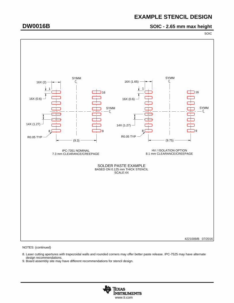
www.ti.com
EXAMPLE STENCIL DESIGN
R0.05 TYPR0.05 TYP
16X (1.65)
16X (0.6)
14X (1.27)
(9.75)
16X (2)
16X (0.6)
14X (1.27)
(9.3)
4221009/B 07/2016
SOIC - 2.65 mm max heightDW0016BSOIC
NOTES: (continued) 8. Laser cutting apertures with trapezoidal walls and rounded corners may offer better paste release. IPC-7525 may have alternate design recommendations. 9. Board assembly site may have different recommendations for stencil design.
SYMM
SYMM
1
8 9
16
HV / ISOLATION OPTION8.1 mm CLEARANCE/CREEPAGE
SOLDER PASTE EXAMPLEBASED ON 0.125 mm THICK STENCIL
SCALE:4X
SYMM
SYMM
1
8 9
16
IPC-7351 NOMINAL7.3 mm CLEARANCE/CREEPAGE

IMPORTANT NOTICE
Texas Instruments Incorporated (TI) reserves the right to make corrections, enhancements, improvements and other changes to itssemiconductor products and services per JESD46, latest issue, and to discontinue any product or service per JESD48, latest issue. Buyersshould obtain the latest relevant information before placing orders and should verify that such information is current and complete.TI’s published terms of sale for semiconductor products (http://www.ti.com/sc/docs/stdterms.htm) apply to the sale of packaged integratedcircuit products that TI has qualified and released to market. Additional terms may apply to the use or sale of other types of TI products andservices.Reproduction of significant portions of TI information in TI data sheets is permissible only if reproduction is without alteration and isaccompanied by all associated warranties, conditions, limitations, and notices. TI is not responsible or liable for such reproduceddocumentation. Information of third parties may be subject to additional restrictions. Resale of TI products or services with statementsdifferent from or beyond the parameters stated by TI for that product or service voids all express and any implied warranties for theassociated TI product or service and is an unfair and deceptive business practice. TI is not responsible or liable for any such statements.Buyers and others who are developing systems that incorporate TI products (collectively, “Designers”) understand and agree that Designersremain responsible for using their independent analysis, evaluation and judgment in designing their applications and that Designers havefull and exclusive responsibility to assure the safety of Designers' applications and compliance of their applications (and of all TI productsused in or for Designers’ applications) with all applicable regulations, laws and other applicable requirements. Designer represents that, withrespect to their applications, Designer has all the necessary expertise to create and implement safeguards that (1) anticipate dangerousconsequences of failures, (2) monitor failures and their consequences, and (3) lessen the likelihood of failures that might cause harm andtake appropriate actions. Designer agrees that prior to using or distributing any applications that include TI products, Designer willthoroughly test such applications and the functionality of such TI products as used in such applications.TI’s provision of technical, application or other design advice, quality characterization, reliability data or other services or information,including, but not limited to, reference designs and materials relating to evaluation modules, (collectively, “TI Resources”) are intended toassist designers who are developing applications that incorporate TI products; by downloading, accessing or using TI Resources in anyway, Designer (individually or, if Designer is acting on behalf of a company, Designer’s company) agrees to use any particular TI Resourcesolely for this purpose and subject to the terms of this Notice.TI’s provision of TI Resources does not expand or otherwise alter TI’s applicable published warranties or warranty disclaimers for TIproducts, and no additional obligations or liabilities arise from TI providing such TI Resources. TI reserves the right to make corrections,enhancements, improvements and other changes to its TI Resources. TI has not conducted any testing other than that specificallydescribed in the published documentation for a particular TI Resource.Designer is authorized to use, copy and modify any individual TI Resource only in connection with the development of applications thatinclude the TI product(s) identified in such TI Resource. NO OTHER LICENSE, EXPRESS OR IMPLIED, BY ESTOPPEL OR OTHERWISETO ANY OTHER TI INTELLECTUAL PROPERTY RIGHT, AND NO LICENSE TO ANY TECHNOLOGY OR INTELLECTUAL PROPERTYRIGHT OF TI OR ANY THIRD PARTY IS GRANTED HEREIN, including but not limited to any patent right, copyright, mask work right, orother intellectual property right relating to any combination, machine, or process in which TI products or services are used. Informationregarding or referencing third-party products or services does not constitute a license to use such products or services, or a warranty orendorsement thereof. Use of TI Resources may require a license from a third party under the patents or other intellectual property of thethird party, or a license from TI under the patents or other intellectual property of TI.TI RESOURCES ARE PROVIDED “AS IS” AND WITH ALL FAULTS. TI DISCLAIMS ALL OTHER WARRANTIES ORREPRESENTATIONS, EXPRESS OR IMPLIED, REGARDING RESOURCES OR USE THEREOF, INCLUDING BUT NOT LIMITED TOACCURACY OR COMPLETENESS, TITLE, ANY EPIDEMIC FAILURE WARRANTY AND ANY IMPLIED WARRANTIES OFMERCHANTABILITY, FITNESS FOR A PARTICULAR PURPOSE, AND NON-INFRINGEMENT OF ANY THIRD PARTY INTELLECTUALPROPERTY RIGHTS. TI SHALL NOT BE LIABLE FOR AND SHALL NOT DEFEND OR INDEMNIFY DESIGNER AGAINST ANY CLAIM,INCLUDING BUT NOT LIMITED TO ANY INFRINGEMENT CLAIM THAT RELATES TO OR IS BASED ON ANY COMBINATION OFPRODUCTS EVEN IF DESCRIBED IN TI RESOURCES OR OTHERWISE. IN NO EVENT SHALL TI BE LIABLE FOR ANY ACTUAL,DIRECT, SPECIAL, COLLATERAL, INDIRECT, PUNITIVE, INCIDENTAL, CONSEQUENTIAL OR EXEMPLARY DAMAGES INCONNECTION WITH OR ARISING OUT OF TI RESOURCES OR USE THEREOF, AND REGARDLESS OF WHETHER TI HAS BEENADVISED OF THE POSSIBILITY OF SUCH DAMAGES.Unless TI has explicitly designated an individual product as meeting the requirements of a particular industry standard (e.g., ISO/TS 16949and ISO 26262), TI is not responsible for any failure to meet such industry standard requirements.Where TI specifically promotes products as facilitating functional safety or as compliant with industry functional safety standards, suchproducts are intended to help enable customers to design and create their own applications that meet applicable functional safety standardsand requirements. Using products in an application does not by itself establish any safety features in the application. Designers mustensure compliance with safety-related requirements and standards applicable to their applications. Designer may not use any TI products inlife-critical medical equipment unless authorized officers of the parties have executed a special contract specifically governing such use.Life-critical medical equipment is medical equipment where failure of such equipment would cause serious bodily injury or death (e.g., lifesupport, pacemakers, defibrillators, heart pumps, neurostimulators, and implantables). Such equipment includes, without limitation, allmedical devices identified by the U.S. Food and Drug Administration as Class III devices and equivalent classifications outside the U.S.TI may expressly designate certain products as completing a particular qualification (e.g., Q100, Military Grade, or Enhanced Product).Designers agree that it has the necessary expertise to select the product with the appropriate qualification designation for their applicationsand that proper product selection is at Designers’ own risk. Designers are solely responsible for compliance with all legal and regulatoryrequirements in connection with such selection.Designer will fully indemnify TI and its representatives against any damages, costs, losses, and/or liabilities arising out of Designer’s non-compliance with the terms and provisions of this Notice.
Mailing Address: Texas Instruments, Post Office Box 655303, Dallas, Texas 75265Copyright © 2017, Texas Instruments Incorporated