igbt gate driver reference design for parallel igbts … gate driver (iso5852s)-8 v_top +15 v_top...
TRANSCRIPT

Isolated Gate Driver (ISO5852S)
-8 V_TOP
+15 V_TOP
DESAT
OUT
+5 V
PWM_TOP
GND PHASE
Isolated Gate Driver (ISO5852S)
-8 V_BOT
+15 V_BOT
DESAT
OUT
+5 V
GND VDC-
PHASE
VDC+
VDC-
1200 V/450 A IGBT MODULE 1
1200 V/450 A
IGBT MODULE 2
PWM_BOT25¶LQJDQG5HVHW
Logic
RESET_N
FAULT_N
READY
RESET_N
FAULT_N
READY
RESET_N
FAULT_N
READY
Copyright © 2016, Texas Instruments Incorporated
1TIDUC70A–December 2016–Revised January 2017Submit Documentation Feedback
Copyright © 2016–2017, Texas Instruments Incorporated
IGBT Gate Driver Reference Design for Parallel IGBTs With Short-CircuitProtection and External BJT Buffer
TI DesignsIGBT Gate Driver Reference Design for Parallel IGBTsWith Short-Circuit Protection and External BJT Buffer
OverviewParalleling IGBTs become necessary for powerconversion equipment with higher output powerratings, where a single IGBT cannot provide therequired load current. This TI Design implements areinforced isolated IGBT gate control module to driveparallel IGBTs in half-bridge configuration. ParallelingIGBTs introduces challenges at both the gate driver(insufficient drive strength) as well as at system levelin maintaining equal current distribution in both theIGBTs while ensuring faster turnon and turnoff. Thisreference design uses reinforced isolated IGBT gatedriver with integrated features like desaturationdetection and soft turnoff to protect the IGBT duringfault conditions. An increased gate drive current (15 A)is obtained through external BJT current booster stagewithout sacrificing the soft turnoff feature. Further, thisdesign demonstrates the mechanism of avoiding gatecurrent loops while operating IGBTs in parallel.
Resources
TIDA-00917 Design FolderISO5852S Product Folder
ASK Our E2E Experts
Features• Suited for Low-Voltage Drives up to 480-VAC
• Designed to Drive Parallel IGBT Modules of a1200-V Rating With Total Gate Charges up to 10µC Translating to Collector Currents of 500 A
• Sourceand Sink Current Ratings of up to 15 ApkWith External BJT Buffer Stage
• Bipolar Gate Drive Voltages• Split Output for Independent Turnon and Turnoff
Control• IGBT Short-Circuit Protection Using Built-in DESAT
and Adjustable Soft Turnoff Time• Built-in Common-Mode Choke and Emitter
Resistance for Limiting Emitter Loop Current• Generates Fault Output During IGBT Short-Circuit
Condition and Gate Driver Undervoltage Scenario• 8000-Vpk VIOTM and 2121-Vpk VIORM Reinforced
Isolation• Very High CMTI of 100 kV/µs
Applications• Variable Speed Drives• UPS• Traction Inverter• Wind and Solar Inverter
An IMPORTANT NOTICE at the end of this TI reference design addresses authorized use, intellectual property matters and otherimportant disclaimers and information.
M
DC BUS +VE
DC BUS -VE
IGBT MODULE
2
IGBT MODULE
1
IGBT MODULE
3
IGBT MODULE
4
IGBT MODULE
5
IGBT MODULE
6
GATE DRIVER MODULE
(TIDA-00917)
Copyright © 2016, Texas Instruments Incorporated
System Overview www.ti.com
2 TIDUC70A–December 2016–Revised January 2017Submit Documentation Feedback
Copyright © 2016–2017, Texas Instruments Incorporated
IGBT Gate Driver Reference Design for Parallel IGBTs With Short-CircuitProtection and External BJT Buffer
1 System Overview
1.1 System DescriptionInsulated gate bipolar transistors (IGBTs) are considerably used in three-phase inverters that havenumerous applications like variable-frequency drives that control the speed of AC motors, uninterruptiblepower supplies (UPS), solar inverters, and other similar inverter applications.
IGBTs have the advantages of high-input impedance as the gate is insulated, has a rapid response ability,good thermal stability, simple driving circuit, good ability to withstand high voltage, snubber-less operation,and controllability of switching behavior providing reliable short-circuit protection. The IGBT is a voltagecontrolled device, which gives it the ability to turn on and off very quickly.
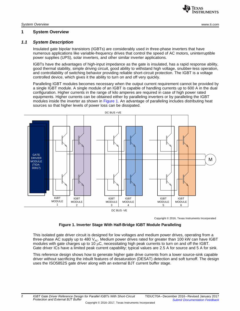
Paralleling IGBT modules becomes necessary when the output current requirement cannot be provided bya single IGBT module. A single module of an IGBT is capable of handling currents up to 600 A in the dualconfiguration. Higher currents in the range of kilo amperes are required in case of high power ratedequipments. Higher currents can be obtained either by paralleling inverters or by paralleling the IGBTmodules inside the inverter as shown in Figure 1. An advantage of paralleling includes distributing heatsources so that higher levels of power loss can be dissipated.
Figure 1. Inverter Stage With Half-Bridge IGBT Module Paralleling
This isolated gate driver circuit is designed for low voltages and medium power drives, operating from athree-phase AC supply up to 480 VAC. Medium power drives rated for greater than 100 kW can have IGBTmodules with gate charges up to 10 μC, necessitating high peak currents to turn on and off the IGBT.Gate driver ICs have a limited peak current capability; typical values are 2.5 A for source and 5 A for sink.
This reference design shows how to generate higher gate drive currents from a lower source-sink capabledriver without sacrificing the inbuilt features of desaturation (DESAT) detection and soft turnoff. The designuses the ISO5852S gate driver along with an external BJT current buffer stage.
www.ti.com System Overview
3TIDUC70A–December 2016–Revised January 2017Submit Documentation Feedback
Copyright © 2016–2017, Texas Instruments Incorporated
IGBT Gate Driver Reference Design for Parallel IGBTs With Short-CircuitProtection and External BJT Buffer
The reference design provides the following key benefits:• High gate source sink current capability due to use of external BJT current buffer stage• IGBT DESAT detection and soft turnoff• Adjustable soft turnoff feature• Optional auto-reset functionality• Reinforced isolation
1.2 Key System Specifications
Table 1. Key System Specifications
FEATURE PARAMETER SPECIFICATION
SystemIGBT module 1200 V, 450 ANumber of IGBT modules 2IGBT module configuration Half bridge
Gate drive
Primary side voltage 5 V ± 5 %Secondary side voltage 24 V ± 5 %Source current / IGBT 7.5 A (max)Sink current / IGBT 7.5 A (max)
Isolation
Creepage 8 mmCMTI 100 KV/µs at VCM= 1500 VIsolation 5700 VRMS per minuteWorking voltage 800 VDC (max)
Protection IGBT overcurrent, undervoltage lockout on both primary and secondary side of gate driver
Isolated Gate Driver (ISO5852S)
-8 V_TOP
+15 V_TOP
DESAT
OUT
+5 V
PWM_TOP
GND PHASE
Isolated Gate Driver (ISO5852S)
-8 V_BOT
+15 V_BOT
DESAT
OUT
+5 V
GND VDC-
PHASE
VDC+
VDC-
1200 V/450 A IGBT MODULE 1
1200 V/450 A
IGBT MODULE 2
PWM_BOT25¶LQJDQG5HVHW
Logic
RESET_N
FAULT_N
READY
RESET_N
FAULT_N
READY
RESET_N
FAULT_N
READY
Copyright © 2016, Texas Instruments Incorporated
System Overview www.ti.com
4 TIDUC70A–December 2016–Revised January 2017Submit Documentation Feedback
Copyright © 2016–2017, Texas Instruments Incorporated
IGBT Gate Driver Reference Design for Parallel IGBTs With Short-CircuitProtection and External BJT Buffer
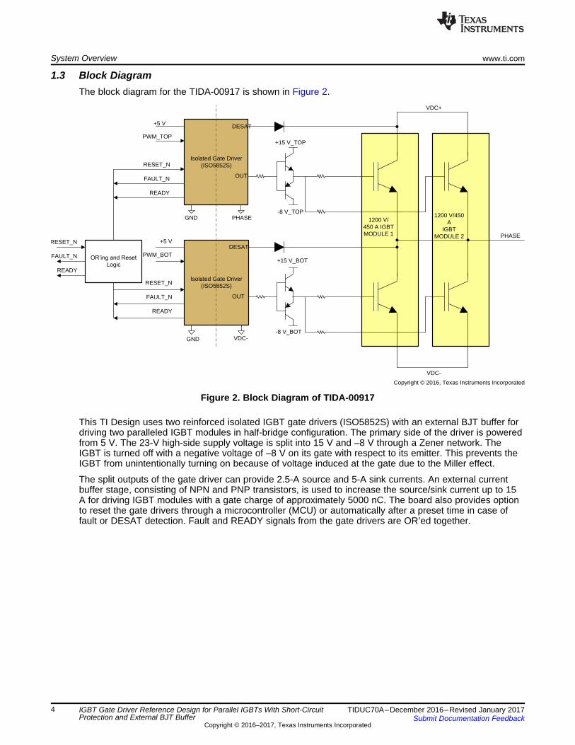
1.3 Block DiagramThe block diagram for the TIDA-00917 is shown in Figure 2.
Figure 2. Block Diagram of TIDA-00917
This TI Design uses two reinforced isolated IGBT gate drivers (ISO5852S) with an external BJT buffer fordriving two paralleled IGBT modules in half-bridge configuration. The primary side of the driver is poweredfrom 5 V. The 23-V high-side supply voltage is split into 15 V and –8 V through a Zener network. TheIGBT is turned off with a negative voltage of –8 V on its gate with respect to its emitter. This prevents theIGBT from unintentionally turning on because of voltage induced at the gate due to the Miller effect.
The split outputs of the gate driver can provide 2.5-A source and 5-A sink currents. An external currentbuffer stage, consisting of NPN and PNP transistors, is used to increase the source/sink current up to 15A for driving IGBT modules with a gate charge of approximately 5000 nC. The board also provides optionto reset the gate drivers through a microcontroller (MCU) or automatically after a preset time in case offault or DESAT detection. Fault and READY signals from the gate drivers are OR’ed together.

ISO5852S
Copyright © 2016, Texas Instruments Incorporated
www.ti.com System Overview
5TIDUC70A–December 2016–Revised January 2017Submit Documentation Feedback
Copyright © 2016–2017, Texas Instruments Incorporated
IGBT Gate Driver Reference Design for Parallel IGBTs With Short-CircuitProtection and External BJT Buffer
1.4 Highlighted ProductsThe TIDA-00917 reference design features the following device from Texas Instruments.
1.4.1 ISO5852SThe ISO5852S is a 5.7-kVRMS, reinforced isolated, IGBT gate driver with split outputs, OUTH and OUTL,providing 2.5-A source and 5-A sink currents. The primary side operates from a single 3-V or 5-V supply.
The output side allows for a supply range from minimum 15 V to maximum 30 V. An internal DESATdetection recognizes when the IGBT is in an overload condition. Upon a DESAT detect, a Mute logicimmediately blocks the output of the isolator and initiates a soft-turnoff procedure, which disables OUTHand reduces the voltage at OUTL over a minimum time span of 2 μs. When OUTL reaches 2 V withrespect to the most negative supply potential, VEE2, the output is hard-clamped to VEE2. During normaloperation with a bipolar output supply, the output is hard clamped to VEE2 when the IGBT is turned off.
Also when DESAT is active, a fault signal is sent across the isolation barrier, pulling FLT output at theinput side low and blocking the isolator input. The FLT output condition is latched and can be reset onlyafter RDY goes high, through a low active pulse at the RST input. This is taken care of by implementingan auto-reset circuit between the Reset and Ready pins.
Figure 3. ISO5852S Functional Block Diagram
For more information on this device, see the ISO5852S product folder at www.TI.com or click on the linkfor the product folder on the first page of this reference design under Resources.
R24
23 V 15 VI 15.66 mA
511
-= =
W
P15V_T
N8V_T
1
2
J2
22-23-2021
15V
D9BZX84J-B15,115
23V TOP
EMITTER_T
+15V, 100mA
-8V, 100mA
511R24
Copyright © 2016, Texas Instruments Incorporated
System Design Theory www.ti.com
6 TIDUC70A–December 2016–Revised January 2017Submit Documentation Feedback
Copyright © 2016–2017, Texas Instruments Incorporated
IGBT Gate Driver Reference Design for Parallel IGBTs With Short-CircuitProtection and External BJT Buffer
2 System Design Theory
2.1 Isolated IGBT Gate DriverThe isolated gate driver is required for driving the top switch of the half-bridge module as the gate voltagehas to be applied with respect to the switch node terminal. Isolation is also required to electrically separatethe low-voltage operator side from the high-voltage drive side to meet safety requirements. This sectiondescribes the design of an isolated gate driver with an external push-pull current buffer stage to increasethe drive capability of the gate driver.
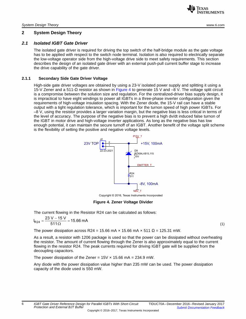
2.1.1 Secondary Side Gate Driver VoltageHigh-side gate driver voltages are obtained by using a 23-V isolated power supply and splitting it using a15-V Zener and a 511-Ω resistor as shown in Figure 4 to generate 15 V and –8 V. The voltage split circuitis a compromise between the solution size and regulation. For the centralized-driver bias supply design, itis impractical to have eight windings to power all IGBTs in a three-phase inverter configuration given therequirements of high-voltage insulation spacing. With the Zener diode, the 15-V rail can have a stableoutput with a tight regulation tolerance, which is important for the turnon speed of high power IGBTs. For–8 V, using the resistor provides a larger variation margin, but the negative bias is less critical in terms ofthe level of accuracy. The purpose of the negative bias is to prevent a high dv/dt induced false turnon ofthe IGBT in motor drive and high-voltage inverter applications. As long as the negative bias has lowenough potential, it can maintain the secure turnoff of an IGBT. Another benefit of the voltage split schemeis the flexibility of setting the positive and negative voltage levels.
Figure 4. Zener Voltage Divider
The current flowing in the Resistor R24 can be calculated as follows:
(1)
The power dissipation across R24 = 15.66 mA × 15.66 mA × 511 Ω = 125.31 mW.
As a result, a resistor with 1206 package is used so that the power can be dissipated without overheatingthe resistor. The amount of current flowing through the Zener is also approximately equal to the currentflowing in the resistor R24. The peak currents required for driving IGBT gate will be supplied from thedecoupling capacitors.
The power dissipation of the Zener = 15V × 15.66 mA = 234.9 mW.
Any diode with the power dissipation value higher than 235 mW can be used. The power dissipationcapacity of the diode used is 550 mW.
VEE21
DESAT
GND23
OUTH
VCC25
OUTL
CLAMP
VEE28
GND1
IN+
IN-
RDY
FAULT
RST
VCC115
GND1
U1
ISO5852SDWR
P5V
0.1µFC2
10.0
R1
DGND
P15V_T
N8V_T
P15V_T
EMITTER_T
0.1µFC11
0.1µFC13
1µFC12
1µFC14
4.7µFC1
Copyright © 2016, Texas Instruments Incorporated
www.ti.com System Design Theory
7TIDUC70A–December 2016–Revised January 2017Submit Documentation Feedback
Copyright © 2016–2017, Texas Instruments Incorporated
IGBT Gate Driver Reference Design for Parallel IGBTs With Short-CircuitProtection and External BJT Buffer
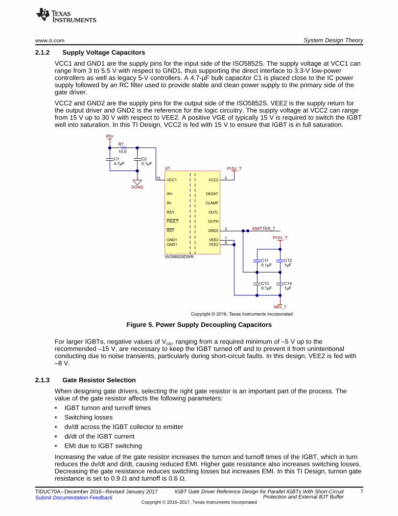
2.1.2 Supply Voltage CapacitorsVCC1 and GND1 are the supply pins for the input side of the ISO5852S. The supply voltage at VCC1 canrange from 3 to 5.5 V with respect to GND1, thus supporting the direct interface to 3.3-V low-powercontrollers as well as legacy 5-V controllers. A 4.7-µF bulk capacitor C1 is placed close to the IC powersupply followed by an RC filter used to provide stable and clean power supply to the primary side of thegate driver.
VCC2 and GND2 are the supply pins for the output side of the ISO5852S. VEE2 is the supply return forthe output driver and GND2 is the reference for the logic circuitry. The supply voltage at VCC2 can rangefrom 15 V up to 30 V with respect to VEE2. A positive VGE of typically 15 V is required to switch the IGBTwell into saturation. In this TI Design, VCC2 is fed with 15 V to ensure that IGBT is in full saturation.
Figure 5. Power Supply Decoupling Capacitors
For larger IGBTs, negative values of VGE, ranging from a required minimum of –5 V up to therecommended –15 V, are necessary to keep the IGBT turned off and to prevent it from unintentionalconducting due to noise transients, particularly during short-circuit faults. In this design, VEE2 is fed with–8 V.
2.1.3 Gate Resistor SelectionWhen designing gate drivers, selecting the right gate resistor is an important part of the process. Thevalue of the gate resistor affects the following parameters:• IGBT turnon and turnoff times• Switching losses• dv/dt across the IGBT collector to emitter• di/dt of the IGBT current• EMI due to IGBT switching
Increasing the value of the gate resistor increases the turnon and turnoff times of the IGBT, which in turnreduces the dv/dt and di/dt, causing reduced EMI. Higher gate resistance also increases switching losses.Decreasing the gate resistance reduces switching losses but increases EMI. In this TI Design, turnon gateresistance is set to 0.9 Ω and turnoff is 0.6 Ω.

total _ sink
Voltage across the IGBT gate 23 VI 9.01 A
Rtotal 2.55= = =
total _ source
Voltage across the IGBT gate 23 VI 8.07 A
Rtotal 2.85= = =
DC_POS
18V
D12SMAJ18CA 10.0k
R25
0.3R70.3R8
0.3R9
1 234
11uH
L1DESAT_T
EMITTER_T
GATE_T_OFFGATE_T_ON
0.01
R34
1
4
7
8
9
10
110.22µFC34
Copyright © 2016, Texas Instruments Incorporated
System Design Theory www.ti.com
8 TIDUC70A–December 2016–Revised January 2017Submit Documentation Feedback
Copyright © 2016–2017, Texas Instruments Incorporated
IGBT Gate Driver Reference Design for Parallel IGBTs With Short-CircuitProtection and External BJT Buffer
2.1.4 Source and Sink CurrentsThe source and sink currents play a major role in determining turnon and turnoff delays of the IGBT.Ideally, the maximum current that can be sourced and sinked into the IGBT can be found as follows:• DC resistance of the common-mode choke = 0.25 Ω• Internal gate resistance of IGBT (FF450R12ME4) = 1.7 Ω• Collector resistance in the ON path (R36) = 0.3 Ω• Rtotal(ON) = Collector resistance in the ON path + R7 + R9 + DC resistance of the common-mode choke
+ Internal gate resistance of IGBT = 0.3 Ω + 0.3 Ω + 0.3 Ω + 0.25 Ω + 1.7 Ω = 2.85 Ω
Figure 6. IGBT Gate Current Control Components
(2)
Similarly, the sink current can be found as follows:• Internal gate resistance of IGBT = 1.7 Ω• Rtotal(OFF) = R8 + R9 + DC resistance of the common-mode choke + Internal gate resistance of IGBT =
0.3 Ω + 0.3 Ω + 0.25 Ω + 1.7 Ω = 2.55 Ω
(3)
www.ti.com System Design Theory
9TIDUC70A–December 2016–Revised January 2017Submit Documentation Feedback
Copyright © 2016–2017, Texas Instruments Incorporated
IGBT Gate Driver Reference Design for Parallel IGBTs With Short-CircuitProtection and External BJT Buffer
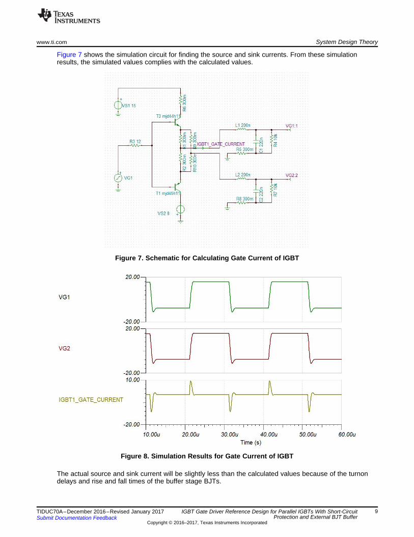
Figure 7 shows the simulation circuit for finding the source and sink currents. From these simulationresults, the simulated values complies with the calculated values.
Figure 7. Schematic for Calculating Gate Current of IGBT
Figure 8. Simulation Results for Gate Current of IGBT
The actual source and sink current will be slightly less than the calculated values because of the turnondelays and rise and fall times of the buffer stage BJTs.
CEDSAT _ transient
D _DSAT
VV
C161
C
=æ ö
+ç ÷ç ÷è ø
CEcharge D _DESAT
dVI C
dt= ´
blank DSTHblank
charge
C V 220 pF 9 Vt 3.96 s
I 0.5 mA
´ ´= = = m
DESAT2
VCC25
P15V_T
1.00k
R2
TP1
EMITTER_T
D4BAT54WS-7-F
12V
D3MMSZ5242BS-7-F220pF
C3
D1
STTH112A
D2
STTH112A
DESAT_T
Copyright © 2016, Texas Instruments Incorporated
System Design Theory www.ti.com
10 TIDUC70A–December 2016–Revised January 2017Submit Documentation Feedback
Copyright © 2016–2017, Texas Instruments Incorporated
IGBT Gate Driver Reference Design for Parallel IGBTs With Short-CircuitProtection and External BJT Buffer
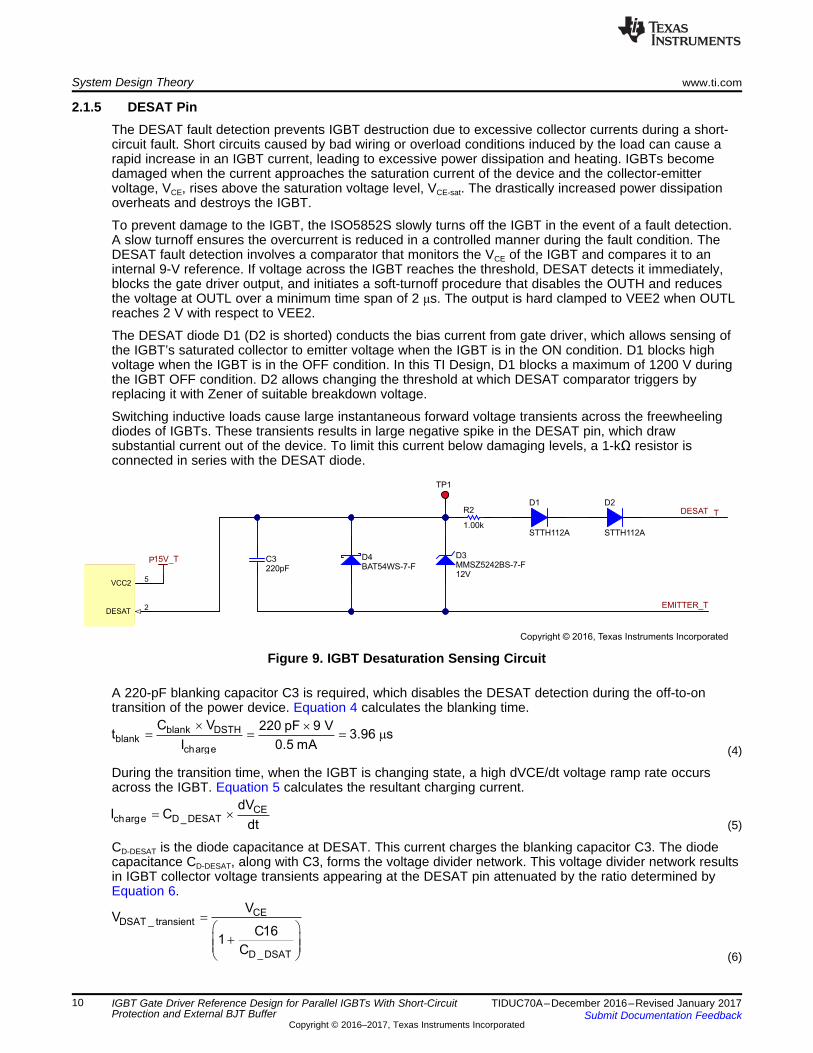
2.1.5 DESAT PinThe DESAT fault detection prevents IGBT destruction due to excessive collector currents during a short-circuit fault. Short circuits caused by bad wiring or overload conditions induced by the load can cause arapid increase in an IGBT current, leading to excessive power dissipation and heating. IGBTs becomedamaged when the current approaches the saturation current of the device and the collector-emittervoltage, VCE, rises above the saturation voltage level, VCE-sat. The drastically increased power dissipationoverheats and destroys the IGBT.
To prevent damage to the IGBT, the ISO5852S slowly turns off the IGBT in the event of a fault detection.A slow turnoff ensures the overcurrent is reduced in a controlled manner during the fault condition. TheDESAT fault detection involves a comparator that monitors the VCE of the IGBT and compares it to aninternal 9-V reference. If voltage across the IGBT reaches the threshold, DESAT detects it immediately,blocks the gate driver output, and initiates a soft-turnoff procedure that disables the OUTH and reducesthe voltage at OUTL over a minimum time span of 2 μs. The output is hard clamped to VEE2 when OUTLreaches 2 V with respect to VEE2.
The DESAT diode D1 (D2 is shorted) conducts the bias current from gate driver, which allows sensing ofthe IGBT’s saturated collector to emitter voltage when the IGBT is in the ON condition. D1 blocks highvoltage when the IGBT is in the OFF condition. In this TI Design, D1 blocks a maximum of 1200 V duringthe IGBT OFF condition. D2 allows changing the threshold at which DESAT comparator triggers byreplacing it with Zener of suitable breakdown voltage.
Switching inductive loads cause large instantaneous forward voltage transients across the freewheelingdiodes of IGBTs. These transients results in large negative spike in the DESAT pin, which drawsubstantial current out of the device. To limit this current below damaging levels, a 1-kΩ resistor isconnected in series with the DESAT diode.
Figure 9. IGBT Desaturation Sensing Circuit
A 220-pF blanking capacitor C3 is required, which disables the DESAT detection during the off-to-ontransition of the power device. Equation 4 calculates the blanking time.
(4)
During the transition time, when the IGBT is changing state, a high dVCE/dt voltage ramp rate occursacross the IGBT. Equation 5 calculates the resultant charging current.
(5)
CD-DESAT is the diode capacitance at DESAT. This current charges the blanking capacitor C3. The diodecapacitance CD-DESAT, along with C3, forms the voltage divider network. This voltage divider network resultsin IGBT collector voltage transients appearing at the DESAT pin attenuated by the ratio determined byEquation 6.
(6)

RST
1
2
3
J4
22-23-2031
RDY
20.0kR30 D10
MBR0520LT1G
P5V
DGND
P5V
20.0kR3
0.01µFC8
Copyright © 2016, Texas Instruments Incorporated
( ) ( )fCE _Fault THV 9 V 0.5 mA 1k 9 1.5 0.5 7 V= - - ´ W = - - =
www.ti.com System Design Theory
11TIDUC70A–December 2016–Revised January 2017Submit Documentation Feedback
Copyright © 2016–2017, Texas Instruments Incorporated
IGBT Gate Driver Reference Design for Parallel IGBTs With Short-CircuitProtection and External BJT Buffer
To avoid false DESAT triggering, fast recovery diodes with low capacitance are used. This design usesthe STTH112A. The STTH112A is a 1-A, 1200-VRRM diode with a reverse recovery time of 75 ns. Theblanking capacitor chosen must have a large value, as a small value will lead to high transient voltage onthe DESAT pin.
The voltage at the DESAT pin equals the sum of the forward voltage drop of D1 and the IGBT collector toemitter voltage. Equation 7 calculates the VCE level that triggers a fault condition.
(7)
2.1.6 Fault DetectionDuring IGBT overcurrent condition, a Mute logic initiates a soft-turnoff procedure that disables OUTH andpulls OUTL to low over a time span through internal constant current sink. When desaturation is active, afault signal is sent across the isolation barrier pulling the FLT output at the input side low and blocking theisolator input. The FLT output condition is latched and can be reset only after RDY goes high, through anactive low pulse at the RST input. The IGBT gate driver is disabled when a fault is detected and will notresume switching until the MCU applies a reset signal of 800 ns.
In this TI Design, an auto-reset circuit shown in Figure 10 has been provided externally. RST is pulledhigh at 5 V using a 20-kΩ resistor and a capacitor value of 0.01 µF. The RDY pin is logic high undernormal conditions and the external Schottky diode is reverse biased so the RST pin also remains high;however, when a fault is encountered, the Ready pin goes low and the Schottky conducts thus pullingdown the RST. By asserting RST low for at least the specified minimum duration (800 ns), the deviceinput logic can be enabled or disabled.
Figure 10. Auto-Reset Circuit
The time it takes for the RST to go high is dependent upon the time constant, which is given by T = RC =20 kΩ × 0.01 µF = 0.2 ms. When RST is pulled down, the circuit resets itself automatically.

12.0R5
12.0R6
0.015µFC39
12.0R10
To BJTOUTL
OUTH
-8 V
Copyright © 2016, Texas Instruments Incorporated
System Design Theory www.ti.com
12 TIDUC70A–December 2016–Revised January 2017Submit Documentation Feedback
Copyright © 2016–2017, Texas Instruments Incorporated
IGBT Gate Driver Reference Design for Parallel IGBTs With Short-CircuitProtection and External BJT Buffer
2.1.7 Adjustable Soft TurnoffIf a short circuit is applied to an IGBT that is already conducting, the dv/dt resulting from the rapiddesaturation of the IGBT would boost the gate voltage of the IGBT and results in higher peak short-circuitcurrent. The increased peak current increases the power dissipation and could cause IGBT failures. Theeffective way of protecting the IGBTs under overcurrent conditions is to use soft turnoff methods.Selectively slowing the IGBT turnoff under overcurrent conditions could reduce the transient voltage spikeapplied on the IGBT and improve the reliability of the system.
After overcurrent detection, the ISO5852S initiates a soft-turnoff procedure that disables OUTH and pullsOUTL to low over a time span of 2 μs. If the IGBT module is directly connected to the gate driver IC, thegate charge of the IGBT is slowly discharged through the internal current sink of the Isolator during turnoff.But in this TI Design, a current booster stage is present in between the driver and the IGBT. Therefore, inorder to provide a soft turnoff of the device, an additional circuit consisting of a resistor, R10, and acapacitor, C39, is connected at the OUTL arm. The capacitor C39 aids in the slow discharging of currentthrough the internal current sink. The soft-turnoff time can easily be adjusted by varying the values of R10and C39, as shown inFigure 11.
Figure 11. Adjustable Soft Turnoff Circuit
2.2 Current Sharing Between Parallel IGBT ModulesIn many high-power applications, the required current levels can only be achieved by connecting two ormore IGBT modules in parallel. When connected in parallel, it is important that the circuit design allows foran equal flow of current to each of the modules. If the current is not balanced among the IGBTs, a highercurrent may build up in just one device and destroy it. Differences on static and dynamic behavior ofparalleled IGBTs affect the current sharing each branch and also de-rate the effective output current.
2.2.1 Static VariationsThese variations are primarily due to the following sources:• VCE-SAT
• Transconductance
Because the two devices are connected in parallel, the conducting stage voltage across the devices is thesame. The static current (Iload = IC2 + IC1) splits as determined by the set of output characteristics, whichin turn are dependent on those two factors.
Selecting a proper IGBT with a positive temperature co-efficient as well as less parametric variation is thekey in overcoming the imbalance in current.

ge2 ge Rg2 Zpar2V V V V= - -
ge1 ge Rg1 Zpar1V V V V= - -
www.ti.com System Design Theory
13TIDUC70A–December 2016–Revised January 2017Submit Documentation Feedback
Copyright © 2016–2017, Texas Instruments Incorporated
IGBT Gate Driver Reference Design for Parallel IGBTs With Short-CircuitProtection and External BJT Buffer
2.2.2 Dynamic VariationsThe dynamic current imbalance is mainly due to the following parameters:• The distribution of device parameters, for example, the threshold voltage VGE(th) and the switching
characteristics of IGBT, especially the gate-emitter capacitance and miller capacitance.• The propagation delay through the gate drive circuit.• The parasitic inductance in the paralleled branches.
The turnon delay of the IGBT is dependent on the threshold Voltage VGE(th), the gate resistance and theequivalent input capacitance of the IGBT. So if the two devices are not turning on at the same time, thenthe one that is turning faster has to carry more current at that moment.
If one of the IGBT has lower value of VGE(th) or gate capacitance then it will turn on faster than the otherone. If the driver had one common gate resistance, then during the Miller region of the faster IGBT, thegate voltage of the slower device will not be able to rise and it will remain off. As a result, the collectorcurrent will not be shared between the two devices with majority passing only through the faster IGBTduring transition. To avoid this, two separate gate resistors have been provided in the gate drive path,which helps the gate voltage of the paralleled IGBTs increases independently. Providing a gate resistor foreach IGBT also reduces the possibility of oscillations between the paralleled devices.
The rate of rise of collector currents will dependent on the parasitic inductances on the emitter side of theIGBTs, which is another contributing factor for the mismatch in the dynamic current shared between thetwo devices. See Section 2.2.3 for more info.
In order to match the switching speeds of the paralleled devices as much as possible, proper layouttechniques are essential. To achieve this, the layout must be as symmetrical as possible to match theparasitic inductances as closely as possible. Minimizing the impedance and impedance mismatch is veryimportant. See Section 5.3 for more details.
2.2.3 Common Emitter InductanceSome stray inductance is present at the emitter of the IGBT modules. The value of stray inductance forthe two IGBTs could differ. Because the IGBTs are connected in parallel, the common ground voltage willremain the same for both the IGBTs but the auxiliary emitter voltages will differ. This voltage differencebetween the auxiliary emitter terminals of the two IGBTs results in current flow from one terminal to theother as shown in Figure 12. Depending on the direction of the circulating current the actual voltage at theIGBT gates will either increase or decrease resulting in unequal current sharing.
The voltage at the gate of the IGBTs is given by Equation 8 and Equation 9.
(8)
(9)
where:• Rg1 and Rg2 are the gate resistors• Zpar1 and Zpar2 are the parasitic track impedances

e2Ls2 s2
di 150 AV L 5 nH 0.75 V
dt s= ´ = ´ =
m
e1Ls1 s1
di 150 AV L 10 nH 1.5 V
dt s= ´ = ´ =
m
Q1 Q2Rg1 Rg2
Gate Driver
10 nHLs1
+
-5 nHLs2
+
-
GND
Choke 1 Choke 2
GND
Vge1 Vge2Vge
Q1 Q2Rg1 Rg2
Gate Driver
10 nHLs1
+
-5 nHLs2
+
-
GND
GND
Vge1 Vge2Vge
Re1 Re2
Zpar1 Zpar2
Copyright © 2016, Texas Instruments Incorporated
System Design Theory www.ti.com
14 TIDUC70A–December 2016–Revised January 2017Submit Documentation Feedback
Copyright © 2016–2017, Texas Instruments Incorporated
IGBT Gate Driver Reference Design for Parallel IGBTs With Short-CircuitProtection and External BJT Buffer
Figure 12. Effect of Parasitic Emitter Inductance
Assuming equal current sharing and equal di/dt during turnon in both the parallel connected IGBTs, theinduced voltage across the stray inductances can be calculated in Equation 10 and Equation 11.
(10)
(11)
where:• Ls1 is the stray inductance of the connection between the emitter of Q1 and the common ground• Ls2 is the stray inductance of the connection between the emitter of Q2 and the common ground• die1/dt is the rate of change of current through Q1 during turnon• die2/dt is the rate of change of current through Q2 during turnon
The drop of 0.75 V between the two auxiliary emitter terminals causes a circulating current Icir throughZpar1 and Zpar2. The gate voltage Vge1 decreases by Icir × Zpar1 and the gate voltage Vge2 increasesby Icir × Zpar2 causing both IGBT modules to turn on at slightly different instants resulting in unequalcurrent sharing.
www.ti.com System Design Theory
15TIDUC70A–December 2016–Revised January 2017Submit Documentation Feedback
Copyright © 2016–2017, Texas Instruments Incorporated
IGBT Gate Driver Reference Design for Parallel IGBTs With Short-CircuitProtection and External BJT Buffer
There are two ways in which the circulating current can be overcome:1. Addition of emitter gate resistor Re1. This helps in attenuating the circulating current.2. Use of common-mode choke in the gate path. The effect of common mode choke is explained in detail
in Section 2.2.4
2.2.4 Common-Mode ChokeA common-mode choke works as a simple wire against a differential mode current. The differential modecurrent flows in opposite directions through the choke windings and creates equal and opposite magneticfields, which cancel each other out. This results in the choke presenting zero impedance to the differentialmode signal. Thus, the differential signal passes through the choke unattenuated.
The common-mode choke works as inductor against a common-mode current. The common-modecurrent, flowing in the same direction through each of the choke windings, creates equal and in-phasemagnetic fields, which add together. The magnetic flux caused by the common-mode current isaccumulated and hence produces impedance. The choke presents a high impedance to the common-mode signal, which passes through the choke heavily attenuated.
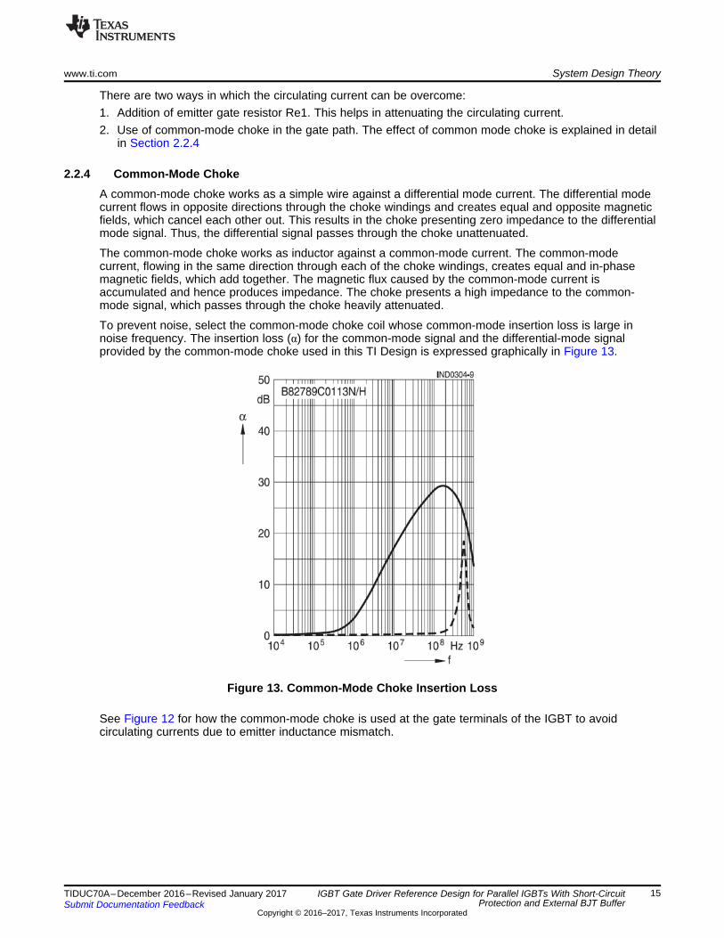
To prevent noise, select the common-mode choke coil whose common-mode insertion loss is large innoise frequency. The insertion loss (α) for the common-mode signal and the differential-mode signalprovided by the common-mode choke used in this TI Design is expressed graphically in Figure 13.
Figure 13. Common-Mode Choke Insertion Loss
See Figure 12 for how the common-mode choke is used at the gate terminals of the IGBT to avoidcirculating currents due to emitter inductance mismatch.

Connector J3 for supplying 23-V to the Bottom IGBT driver
Connector J1 containing 5 V supply pin, ground pin, PWM input for Top and Bottom side, and
fault indication pin
Connector J4 for Reset and Ready signal
indicationConnector J2 for
supplying 23 V to the top IGBT driver
Getting Started Hardware www.ti.com
16 TIDUC70A–December 2016–Revised January 2017Submit Documentation Feedback
Copyright © 2016–2017, Texas Instruments Incorporated
IGBT Gate Driver Reference Design for Parallel IGBTs With Short-CircuitProtection and External BJT Buffer
3 Getting Started Hardware
3.1 Board DescriptionFigure 14 shows the TIDA-00917 board mounted on IGBT modules. The board has to be powered up bysupplying the primary side voltage of 5 V and secondary side voltage of 23 V. The 5-V supply is providedusing the connector J1 and 23-V supply is provided by using the connector J2 and J3 for the top andbottom IGBT driver, respectively. After powering up the board, the status of the Ready pin can be checkedto ensure that there is no problem with the supply voltages. Connector J4 provides a pin to indicate theReady signal. Now the PWM signal can be applied to the connector J1 for the top and bottom IGBTs, andthe output can be observed in the form of a gate voltage of the IGBTs.
Figure 14. Board Description

www.ti.com Getting Started Hardware
17TIDUC70A–December 2016–Revised January 2017Submit Documentation Feedback
Copyright © 2016–2017, Texas Instruments Incorporated
IGBT Gate Driver Reference Design for Parallel IGBTs With Short-CircuitProtection and External BJT Buffer
3.2 Connector Description
Table 2. Connector Pin Description
CONNECTOR PIN NUMBER PIN NAME I/O DESCRIPTION
J1
1 P5V PWR Primary side supply voltage2 DGND PWR Ground pin3 PWM_IN_TOP I PWM signal for top IGBT gate driver4 PWM_IN_BOTTOM I PWM signal for bottom IGBT gate driver
5 FLT O Active low if any of the IGBT driver detectdesaturation of associated IGBT
6 DGND PWR Ground pin
J21 P15V_T PWR VCC2 for top IGBT gate driver2 P8V_T PWR VEE2 for top IGBT gate driver
J31 P15V_B PWR VCC2 for bottom IGBT gate driver2 P8V_B PWR VEE2 for bottom IGBT gate driver
J4
1 RDY O Power-good output, active high when bothsupplies are healthy
2 RST I Reset input, apply a low pulse to reset faultlatch
3 DGND PWR Ground pin
Gate to Emitter VoltageFall of VCC2 from 15 V to 0 VInput PWM
Testing and Results www.ti.com
18 TIDUC70A–December 2016–Revised January 2017Submit Documentation Feedback
Copyright © 2016–2017, Texas Instruments Incorporated
IGBT Gate Driver Reference Design for Parallel IGBTs With Short-CircuitProtection and External BJT Buffer
4 Testing and Results
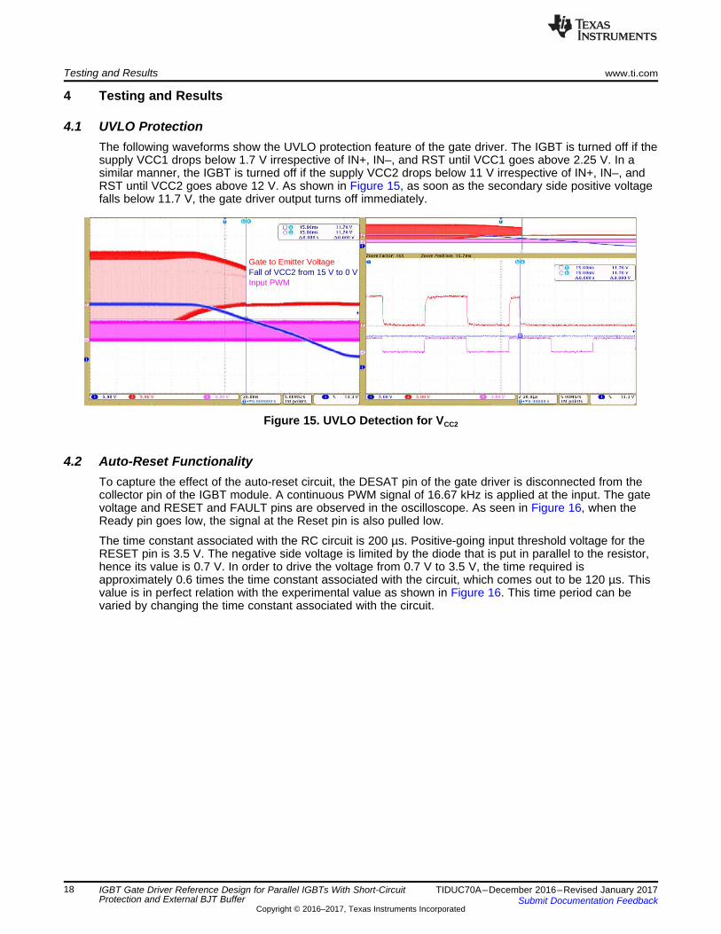
4.1 UVLO ProtectionThe following waveforms show the UVLO protection feature of the gate driver. The IGBT is turned off if thesupply VCC1 drops below 1.7 V irrespective of IN+, IN–, and RST until VCC1 goes above 2.25 V. In asimilar manner, the IGBT is turned off if the supply VCC2 drops below 11 V irrespective of IN+, IN–, andRST until VCC2 goes above 12 V. As shown in Figure 15, as soon as the secondary side positive voltagefalls below 11.7 V, the gate driver output turns off immediately.
Figure 15. UVLO Detection for VCC2
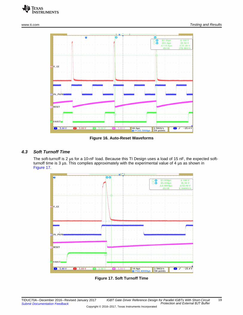
4.2 Auto-Reset FunctionalityTo capture the effect of the auto-reset circuit, the DESAT pin of the gate driver is disconnected from thecollector pin of the IGBT module. A continuous PWM signal of 16.67 kHz is applied at the input. The gatevoltage and RESET and FAULT pins are observed in the oscilloscope. As seen in Figure 16, when theReady pin goes low, the signal at the Reset pin is also pulled low.
The time constant associated with the RC circuit is 200 µs. Positive-going input threshold voltage for theRESET pin is 3.5 V. The negative side voltage is limited by the diode that is put in parallel to the resistor,hence its value is 0.7 V. In order to drive the voltage from 0.7 V to 3.5 V, the time required isapproximately 0.6 times the time constant associated with the circuit, which comes out to be 120 µs. Thisvalue is in perfect relation with the experimental value as shown in Figure 16. This time period can bevaried by changing the time constant associated with the circuit.
www.ti.com Testing and Results
19TIDUC70A–December 2016–Revised January 2017Submit Documentation Feedback
Copyright © 2016–2017, Texas Instruments Incorporated
IGBT Gate Driver Reference Design for Parallel IGBTs With Short-CircuitProtection and External BJT Buffer
Figure 16. Auto-Reset Waveforms
4.3 Soft Turnoff TimeThe soft-turnoff is 2 µs for a 10-nF load. Because this TI Design uses a load of 15 nF, the expected soft-turnoff time is 3 µs. This complies approximately with the experimental value of 4 µs as shown inFigure 17.
Figure 17. Soft Turnoff Time
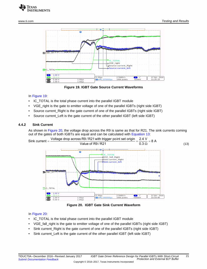
Voltage drop across R9 / R21 with trigger point set origin 2 VSource current 6.67 A
Value of R9 / R21 0.3= = =
W
Left-side IGBT gate
Right-side IGBT gate
Testing and Results www.ti.com
20 TIDUC70A–December 2016–Revised January 2017Submit Documentation Feedback
Copyright © 2016–2017, Texas Instruments Incorporated
IGBT Gate Driver Reference Design for Parallel IGBTs With Short-CircuitProtection and External BJT Buffer
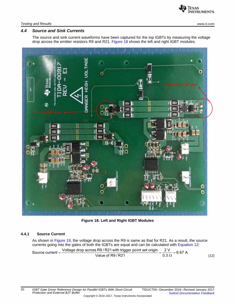
4.4 Source and Sink CurrentsThe source and sink current waveforms have been captured for the top IGBTs by measuring the voltagedrop across the emitter resistors R9 and R21. Figure 18 shows the left and right IGBT modules.
Figure 18. Left and Right IGBT Modules
4.4.1 Source CurrentAs shown in Figure 19, the voltage drop across the R9 is same as that for R21. As a result, the sourcecurrents going into the gates of both the IGBTs are equal and can be calculated with Equation 12:
(12)
Voltage drop across R9 / R21 with trigger point set origin 2.4 VSink current 8 A
Value of R9 / R21 0.3= = =
W
www.ti.com Testing and Results
21TIDUC70A–December 2016–Revised January 2017Submit Documentation Feedback
Copyright © 2016–2017, Texas Instruments Incorporated
IGBT Gate Driver Reference Design for Parallel IGBTs With Short-CircuitProtection and External BJT Buffer
Figure 19. IGBT Gate Source Current Waveforms
In Figure 19:• IC_TOTAL is the total phase current into the parallel IGBT module• VGE_right is the gate to emitter voltage of one of the parallel IGBTs (right side IGBT)• Source current_Right is the gate current of one of the parallel IGBTs (right side IGBT)• Source current_Left is the gate current of the other parallel IGBT (left side IGBT)
4.4.2 Sink CurrentAs shown in Figure 20, the voltage drop across the R9 is same as that for R21. The sink currents comingout of the gates of both IGBTs are equal and can be calculated with Equation 13:
(13)
Figure 20. IGBT Gate Sink Current Waveform
In Figure 20:• IC_TOTAL is the total phase current into the parallel IGBT module• VGE_fall_right is the gate to emitter voltage of one of the parallel IGBTs (right side IGBT)• Sink current_Right is the gate current of one of the parallel IGBTs (right side IGBT)• Sink current_Left is the gate current of the other parallel IGBT (left side IGBT)
5 V Supply
Function Generator
23 V Supply from TIDA-00702
Board
23 V Supply from TIDA-00702
Board
ISO
5852SIS
O5852S
Top IGBT Gate Driver
Bottom IGBT Gate
Driver
C
E
G
C
E
G
600 V Supply
C
E
G
C
E
G
4.7
Probing points for current measurement
Copyright © 2016, Texas Instruments Incorporated
Testing and Results www.ti.com
22 TIDUC70A–December 2016–Revised January 2017Submit Documentation Feedback
Copyright © 2016–2017, Texas Instruments Incorporated
IGBT Gate Driver Reference Design for Parallel IGBTs With Short-CircuitProtection and External BJT Buffer
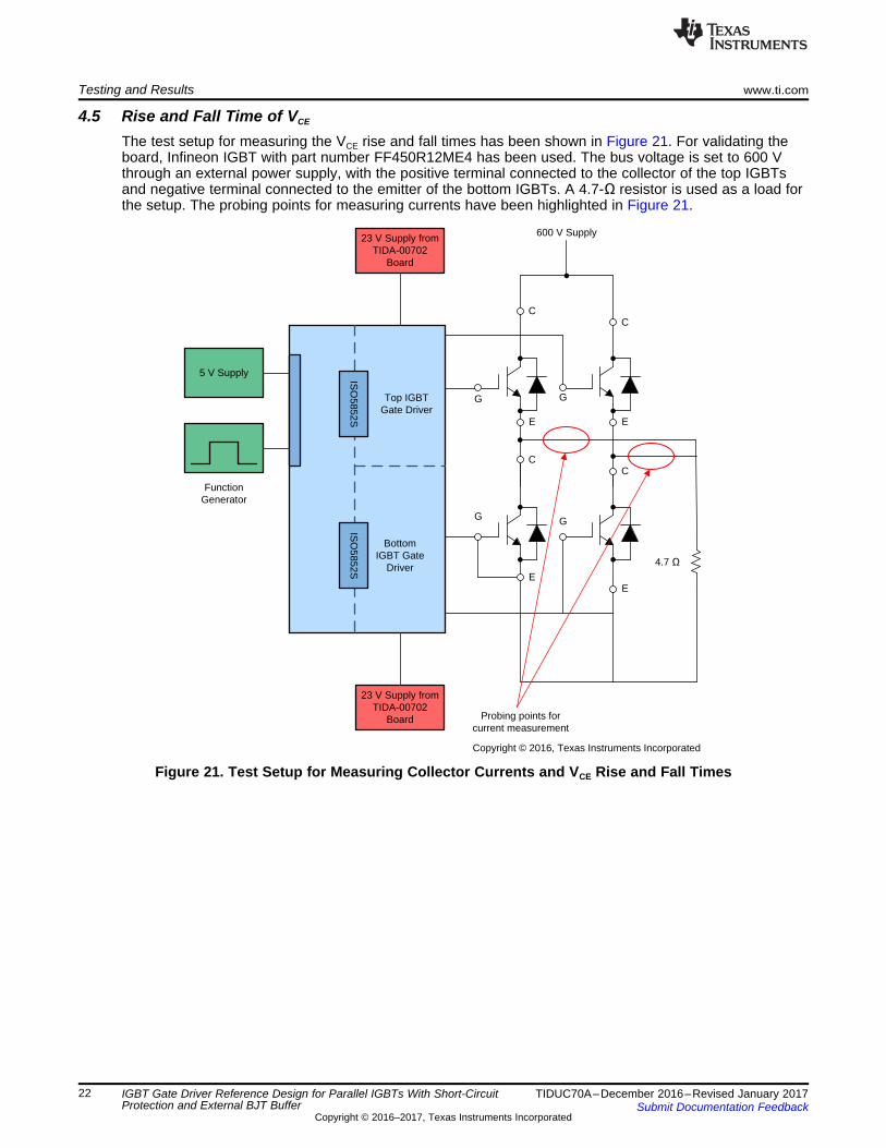
4.5 Rise and Fall Time of VCE
The test setup for measuring the VCE rise and fall times has been shown in Figure 21. For validating theboard, Infineon IGBT with part number FF450R12ME4 has been used. The bus voltage is set to 600 Vthrough an external power supply, with the positive terminal connected to the collector of the top IGBTsand negative terminal connected to the emitter of the bottom IGBTs. A 4.7-Ω resistor is used as a load forthe setup. The probing points for measuring currents have been highlighted in Figure 21.
Figure 21. Test Setup for Measuring Collector Currents and VCE Rise and Fall Times
V_CE
Ic
V_CE
Ic
www.ti.com Testing and Results
23TIDUC70A–December 2016–Revised January 2017Submit Documentation Feedback
Copyright © 2016–2017, Texas Instruments Incorporated
IGBT Gate Driver Reference Design for Parallel IGBTs With Short-CircuitProtection and External BJT Buffer
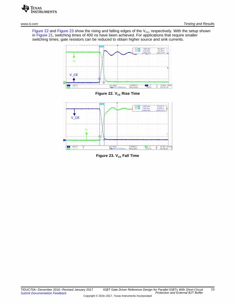
Figure 22 and Figure 23 show the rising and falling edges of the VCE, respectively. With the setup shownin Figure 21, switching times of 400 ns have been achieved. For applications that require smallerswitching times, gate resistors can be reduced to obtain higher source and sink currents.
Figure 22. VCE Rise Time
Figure 23. VCE Fall Time

Left IGBT Current
Right IGBT Vge
Left IGBT Vge
Right IGBT Current
Right IGBT Vge
Left IGBT Vge
Right IGBT Current
Left IGBT Current
Right IGBT Vge
Left IGBT VgeRight IGBT Current
Left IGBT Current
Testing and Results www.ti.com
24 TIDUC70A–December 2016–Revised January 2017Submit Documentation Feedback
Copyright © 2016–2017, Texas Instruments Incorporated
IGBT Gate Driver Reference Design for Parallel IGBTs With Short-CircuitProtection and External BJT Buffer
4.6 Current Sharing Between Right and Left IGBTsFigure 26 shows the current sharing between the top IGBTs when an input pulse of 100 µs is applied tothe primary side of the gate driver. As shown in Figure 24, there is a difference of 20 A between thedynamic current shared by the two devices. This difference is because of the turnon delay time of the twoIGBTs, VCE-SAT, and the parasitic inductances of the paralleled branches. As shown in Figure 25, the staticcurrent shared between the two devices becomes almost equal after a time period of 60 µs as shown inFigure 26.
Figure 24. Current Sharing During IGBT Turnon Figure 25. Current Sharing During IGBT Turnoff
Figure 26. Current Sharing During One PWM Pulse
blankcharge
charge
C V 220 pF 8.8 Vt 3.87 s
I 0.5 mA
´ ´= = = m
5-V supply
Function Generator
23-V supply from TIDA-00702
board
23-V supply from TIDA-00702
board
ISO
5852SIS
O5852S
Top IGBT Gate Driver
Bottom IGBT Gate
Driver
C
E
G
C
E
G
600-V supply
C
E
G
C
E
G
Probing points for current measurement
Copyright © 2016, Texas Instruments Incorporated
15 µH
www.ti.com Testing and Results
25TIDUC70A–December 2016–Revised January 2017Submit Documentation Feedback
Copyright © 2016–2017, Texas Instruments Incorporated
IGBT Gate Driver Reference Design for Parallel IGBTs With Short-CircuitProtection and External BJT Buffer
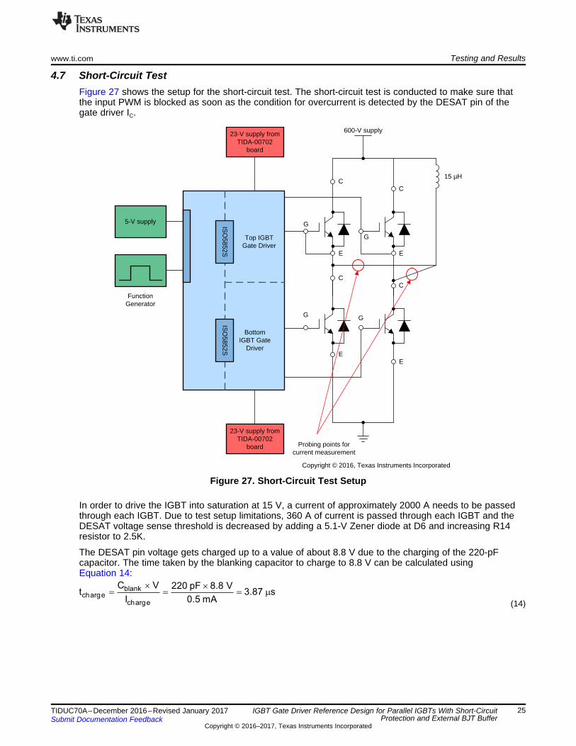
4.7 Short-Circuit TestFigure 27 shows the setup for the short-circuit test. The short-circuit test is conducted to make sure thatthe input PWM is blocked as soon as the condition for overcurrent is detected by the DESAT pin of thegate driver IC.
Figure 27. Short-Circuit Test Setup
In order to drive the IGBT into saturation at 15 V, a current of approximately 2000 A needs to be passedthrough each IGBT. Due to test setup limitations, 360 A of current is passed through each IGBT and theDESAT voltage sense threshold is decreased by adding a 5.1-V Zener diode at D6 and increasing R14resistor to 2.5K.
The DESAT pin voltage gets charged up to a value of about 8.8 V due to the charging of the 220-pFcapacitor. The time taken by the blanking capacitor to charge to 8.8 V can be calculated usingEquation 14:
(14)
DESAT
FAULT
IGBT Current
V_GE
DESAT
V_CE
IGBT Current
V_GE
Testing and Results www.ti.com
26 TIDUC70A–December 2016–Revised January 2017Submit Documentation Feedback
Copyright © 2016–2017, Texas Instruments Incorporated
IGBT Gate Driver Reference Design for Parallel IGBTs With Short-CircuitProtection and External BJT Buffer
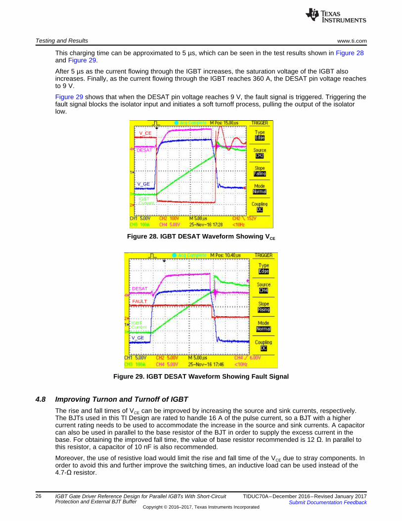
This charging time can be approximated to 5 µs, which can be seen in the test results shown in Figure 28and Figure 29.
After 5 µs as the current flowing through the IGBT increases, the saturation voltage of the IGBT alsoincreases. Finally, as the current flowing through the IGBT reaches 360 A, the DESAT pin voltage reachesto 9 V.
Figure 29 shows that when the DESAT pin voltage reaches 9 V, the fault signal is triggered. Triggering thefault signal blocks the isolator input and initiates a soft turnoff process, pulling the output of the isolatorlow.
Figure 28. IGBT DESAT Waveform Showing VCE
Figure 29. IGBT DESAT Waveform Showing Fault Signal
4.8 Improving Turnon and Turnoff of IGBTThe rise and fall times of VCE can be improved by increasing the source and sink currents, respectively.The BJTs used in this TI Design are rated to handle 16 A of the pulse current, so a BJT with a highercurrent rating needs to be used to accommodate the increase in the source and sink currents. A capacitorcan also be used in parallel to the base resistor of the BJT in order to supply the excess current in thebase. For obtaining the improved fall time, the value of base resistor recommended is 12 Ω. In parallel tothis resistor, a capacitor of 10 nF is also recommended.
Moreover, the use of resistive load would limit the rise and fall time of the VCE due to stray components. Inorder to avoid this and further improve the switching times, an inductive load can be used instead of the4.7-Ω resistor.
www.ti.com Design Files
27TIDUC70A–December 2016–Revised January 2017Submit Documentation Feedback
Copyright © 2016–2017, Texas Instruments Incorporated
IGBT Gate Driver Reference Design for Parallel IGBTs With Short-CircuitProtection and External BJT Buffer
5 Design Files
5.1 SchematicsTo download the schematics, see the design files at TIDA-00917.
5.2 Bill of MaterialsTo download the bill of materials (BOM), see the design files at TIDA-00917.
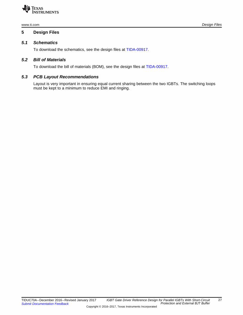
5.3 PCB Layout RecommendationsLayout is very important in ensuring equal current sharing between the two IGBTs. The switching loopsmust be kept to a minimum to reduce EMI and ringing.
Top IGBT gate of module 1
Top IGBT gate of module 2
IGBT gate turnoff track
BJT based push-pull buffer stage to
increase gate current
15-V and -8-V Decoupling capacitors
Gate turnon and turnoff return path
IGBT gate turnon track
Design Files www.ti.com
28 TIDUC70A–December 2016–Revised January 2017Submit Documentation Feedback
Copyright © 2016–2017, Texas Instruments Incorporated
IGBT Gate Driver Reference Design for Parallel IGBTs With Short-CircuitProtection and External BJT Buffer
Figure 30. Current Buffer Stage Interface to IGBT Gate
Figure 30 shows the location of the gates of the two IGBT modules connected in parallel. Also shown arethe IGBT turnon and turnoff gate current paths and the gate current return path. Both are driven from asingle push-pull buffer stage. The following guidelines ensure reliable operation:• Place the 15-V and –8-V decoupling capacitors close to the BJT buffer stage. This ensures the
smallest possible gate current drive loop area.• Connect the output of the push-pull buffer stage to the gate drive tracks in such a way that the distance
to each of the IGBT gates is equal as shown in Figure 31.

Place external gate decoupling capacitor and 10k resistor in parallel very close to the IGBT module gate.
Place on/off gate resistors and common-mode choke close to the IGBT gate
Connect the buffer at the center of the gate tracks so that the distance from buffer to each of the IGBT module gates is equal
www.ti.com Design Files
29TIDUC70A–December 2016–Revised January 2017Submit Documentation Feedback
Copyright © 2016–2017, Texas Instruments Incorporated
IGBT Gate Driver Reference Design for Parallel IGBTs With Short-CircuitProtection and External BJT Buffer
Figure 31. Connection of Buffer to Gate Track
• Make the gate on and off current tracks as wide as possible to minimize track impedance.• Place the external gate decoupling capacitor right next to the module gate.• Place the 10-kΩ resistor next to the decoupling cap. This resistor ensures that the IGBT is turned off in
case the gate drive is floating due to faulty conditions.• Place the common-mode choke and the gate current control resistors close to the module gate.• Maintain a minimum spacing of 8 mm between the primary and secondary sides to ensure reinforced
isolation as shown in Figure 32.
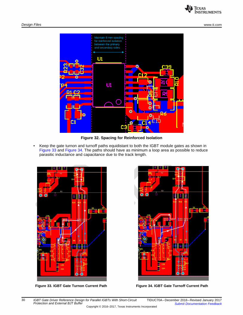
Maintain 8-mm spacing for reinforced isolation between the primary and secondary sides
Design Files www.ti.com
30 TIDUC70A–December 2016–Revised January 2017Submit Documentation Feedback
Copyright © 2016–2017, Texas Instruments Incorporated
IGBT Gate Driver Reference Design for Parallel IGBTs With Short-CircuitProtection and External BJT Buffer
Figure 32. Spacing for Reinforced Isolation
• Keep the gate turnon and turnoff paths equidistant to both the IGBT module gates as shown inFigure 33 and Figure 34. The paths should have as minimum a loop area as possible to reduceparasitic inductance and capacitance due to the track length.
Figure 33. IGBT Gate Turnon Current Path Figure 34. IGBT Gate Turnoff Current Path

www.ti.com Design Files
31TIDUC70A–December 2016–Revised January 2017Submit Documentation Feedback
Copyright © 2016–2017, Texas Instruments Incorporated
IGBT Gate Driver Reference Design for Parallel IGBTs With Short-CircuitProtection and External BJT Buffer
5.3.1 Layout PrintsTo download the layer plots, see the design files at TIDA-00917.
5.4 Altium ProjectTo download the Altium project files, see the design files at TIDA-00917.
5.5 Gerber FilesTo download the Gerber files, see the design files at TIDA-00917.
5.6 Assembly DrawingsTo download the assembly drawings, see the design files at TIDA-00917.
6 References
1. Texas Instruments, High-voltage reinforced isolation: Definitions and test methodologies, MarketingWhite Paper (SLYY063)
2. Texas Instruments, 60-W, 24-V, High-Efficiency Industrial Power Supply With Precision Voltage,Current, and Power Limit, TIDA-00702 Design Guide (TIDUB51)
6.1 TrademarksAll trademarks are the property of their respective owners.
7 Terminology
IGBT— Insulated gate bipolar transistor
PWM— Pulse width modulation
NTC— Negative temperature coefficient thermistor
8 About the AuthorsAISHWARYA BHATNAGAR is a systems engineer at Texas Instruments, where she is responsible fordeveloping reference design solutions for the Motor Drive segment within Industrial Systems. Aishwaryaearned her bachelor of technology in electronics and communication engineering from MNNIT, Allahabad.
PAWAN NAYAK is a systems engineer at Texas Instruments, where he is responsible for developingreference design solutions for the Motor Drive segment within Industrial Systems.
N. NAVANEETH KUMAR is a systems architect at Texas Instruments, where he is responsible fordeveloping subsystem solutions for motor controls within Industrial Systems. N. Navaneeth brings to thisrole his extensive experience in power electronics, EMC, analog, and mixed signal designs. He hassystem-level product design experience in drives, solar inverters, UPS, and protection relays. N.Navaneeth earned his bachelor of electronics and communication engineering from Bharathiar University,India and his master of science in electronic product development from Bolton University, UK.

Revision A History www.ti.com
32 TIDUC70A–December 2016–Revised January 2017Submit Documentation Feedback
Copyright © 2016–2017, Texas Instruments Incorporated
Revision History
Revision A HistoryNOTE: Page numbers for previous revisions may differ from page numbers in the current version.
Changes from Original (December 2016) to A Revision ................................................................................................ Page
• Changed language and images to fit current style guide ............................................................................ 1

IMPORTANT NOTICE FOR TI DESIGN INFORMATION AND RESOURCES
Texas Instruments Incorporated (‘TI”) technical, application or other design advice, services or information, including, but not limited to,reference designs and materials relating to evaluation modules, (collectively, “TI Resources”) are intended to assist designers who aredeveloping applications that incorporate TI products; by downloading, accessing or using any particular TI Resource in any way, you(individually or, if you are acting on behalf of a company, your company) agree to use it solely for this purpose and subject to the terms ofthis Notice.TI’s provision of TI Resources does not expand or otherwise alter TI’s applicable published warranties or warranty disclaimers for TIproducts, and no additional obligations or liabilities arise from TI providing such TI Resources. TI reserves the right to make corrections,enhancements, improvements and other changes to its TI Resources.You understand and agree that you remain responsible for using your independent analysis, evaluation and judgment in designing yourapplications and that you have full and exclusive responsibility to assure the safety of your applications and compliance of your applications(and of all TI products used in or for your applications) with all applicable regulations, laws and other applicable requirements. Yourepresent that, with respect to your applications, you have all the necessary expertise to create and implement safeguards that (1)anticipate dangerous consequences of failures, (2) monitor failures and their consequences, and (3) lessen the likelihood of failures thatmight cause harm and take appropriate actions. You agree that prior to using or distributing any applications that include TI products, youwill thoroughly test such applications and the functionality of such TI products as used in such applications. TI has not conducted anytesting other than that specifically described in the published documentation for a particular TI Resource.You are authorized to use, copy and modify any individual TI Resource only in connection with the development of applications that includethe TI product(s) identified in such TI Resource. NO OTHER LICENSE, EXPRESS OR IMPLIED, BY ESTOPPEL OR OTHERWISE TOANY OTHER TI INTELLECTUAL PROPERTY RIGHT, AND NO LICENSE TO ANY TECHNOLOGY OR INTELLECTUAL PROPERTYRIGHT OF TI OR ANY THIRD PARTY IS GRANTED HEREIN, including but not limited to any patent right, copyright, mask work right, orother intellectual property right relating to any combination, machine, or process in which TI products or services are used. Informationregarding or referencing third-party products or services does not constitute a license to use such products or services, or a warranty orendorsement thereof. Use of TI Resources may require a license from a third party under the patents or other intellectual property of thethird party, or a license from TI under the patents or other intellectual property of TI.TI RESOURCES ARE PROVIDED “AS IS” AND WITH ALL FAULTS. TI DISCLAIMS ALL OTHER WARRANTIES ORREPRESENTATIONS, EXPRESS OR IMPLIED, REGARDING TI RESOURCES OR USE THEREOF, INCLUDING BUT NOT LIMITED TOACCURACY OR COMPLETENESS, TITLE, ANY EPIDEMIC FAILURE WARRANTY AND ANY IMPLIED WARRANTIES OFMERCHANTABILITY, FITNESS FOR A PARTICULAR PURPOSE, AND NON-INFRINGEMENT OF ANY THIRD PARTY INTELLECTUALPROPERTY RIGHTS.TI SHALL NOT BE LIABLE FOR AND SHALL NOT DEFEND OR INDEMNIFY YOU AGAINST ANY CLAIM, INCLUDING BUT NOTLIMITED TO ANY INFRINGEMENT CLAIM THAT RELATES TO OR IS BASED ON ANY COMBINATION OF PRODUCTS EVEN IFDESCRIBED IN TI RESOURCES OR OTHERWISE. IN NO EVENT SHALL TI BE LIABLE FOR ANY ACTUAL, DIRECT, SPECIAL,COLLATERAL, INDIRECT, PUNITIVE, INCIDENTAL, CONSEQUENTIAL OR EXEMPLARY DAMAGES IN CONNECTION WITH ORARISING OUT OF TI RESOURCES OR USE THEREOF, AND REGARDLESS OF WHETHER TI HAS BEEN ADVISED OF THEPOSSIBILITY OF SUCH DAMAGES.You agree to fully indemnify TI and its representatives against any damages, costs, losses, and/or liabilities arising out of your non-compliance with the terms and provisions of this Notice.This Notice applies to TI Resources. Additional terms apply to the use and purchase of certain types of materials, TI products and services.These include; without limitation, TI’s standard terms for semiconductor products http://www.ti.com/sc/docs/stdterms.htm), evaluationmodules, and samples (http://www.ti.com/sc/docs/sampterms.htm).
Mailing Address: Texas Instruments, Post Office Box 655303, Dallas, Texas 75265Copyright © 2017, Texas Instruments Incorporated