keyboard encoder circuits - willegal.net · keyboard encoder circuits ... vss ,-0.75 -4.5 vss - 1.0...
TRANSCRIPT


Keyboard Encoder Circuits
MM5740 gO-key keyboard encoder
general description
The MM5740 MaS/LSI keyboard encoder is a complete keyboard interface system capable of encoding 90 single pole single throw switch closures into a usable 9-bit code. It is organized as a bit paired system and is capable of N key or two key rollover. The MM5740 is fabricated with silicon gate technology and provides for direct TTL!DTL compatibility on Data and Str'abe outputs without the use of any special interface components.
features
• TRI-STATE® data outputs directly compatible with rrUDTl or MOS logic
• Function inputs directly compatible with TTL! DTL logic
block and connection diagrams
For additional application information, see AN-128 and AN-139 at the end of this section.
• Only one TTL level clock required
• N key/two key rollover (mask programmable)
• 90 key-quad mode capability
• One 'character data storage
• Repeat function (selectable)
• Shift lock with indicator capability
• Key bounce masking by single external capacitor
• Level or pulse data strobe output
• Data strobe pu Ise width control
." aDU~~~ ~ .. Dual-I n·Line Package
40 ¥ -=-- a.o.u v" " JO "
1+------Ofo~~~~L
'''"'' l-r-~=---.--J~;;:~I OATA
:~::; o-----~
SHllr WN1RO'
TRt-STATE is a registered trademark of National Semiconductor Corp.
10-2
OUTPUT EIIABLE
" .. XB 16 B8
X7
l3 B5 J1 V·i ,
Xl 10
" " GAlA STROBE OUTPUT " " O~T,~ STROBE CONTROL '5
OUTPUT ENA8LE
REPEAT " X E Y ilOUNCE MASK
VCO IB
COI'lTROl " SHIFT lOCk liO
TOPVIEW
Order Number MM5740N See Pa.kage 24

absolute maximum ratings Data and Clock Input Voltages and Supply
Voltages with Respect to Vss Power Dissipation
Operating Temperature
Storage Temperature
+0.3V to -20V 600 mW at T A C +25°C
-25°C to + 70ce ambient -65°e to +160°C
Lead Temperature (Soldering, 10 seconds) 300D e
electrical cha racte ristics (Note 1,51
PARAMETER
Clock Repetition Rate
Clock Pulse Width
Clock Amplitude
Logic Level "0" Logic Level "1"
Clock Transit ion Times
Risetime Fulltime
Clock Input Capilcitance
Data Input Levels, Yl thru Y10
Logic Level "0" Logic Level" 1 "
LogiC Level "a" Logic Level" 1 "
Dati! Strobe Control Logic Leve l "0"
Logic Level" 1 "
Data Output Levt!ls, Xl thru X9
Logic Level "0"
Logic L evel" 1"
Bl thru 89 and Data Strobe logic Level "0" Logic Level" 1 "
Shift Lock Voltage Open
Shift Lock Voltage Closed
Shift Lock Voltage Locked
·Transition Times
Data Strobe (T DS1)
Data Strobe '(T Ds61
Data Output Levels
(T 001)
~ T 000)
Output Enable Setup Time IT OES I
OUTput Enable Release Time (TOER )
Repeat I nput Pulse Width (T RPW)
Power Supply Cur rent
CONDITIONS
Rep. Rate = 200 kHz
Rep. Rate = 10kHz
Rep. Rate = 200 kHz Rep. Rate = 200 kHz
When Connected to Yl thru Y 10
via S~'Vitch Matrix. (C L "'" 75 pF )
I " 100~A INote 21 I =0 L6 mA (Note 2)
Before Closure
Switch Closed
After ReleClse, (I = 1.0 mAl
(Figure 2)
C L " 100 pF, I ~ 1.6 rnA
CL " 100 pF, I = 100~A
CL " 100pF, I ~ 1.6 rnA
CL " 100 pF, I ' 100~A
INote 31
fCLOCK = 10'kHz fe'L OCK c= 200 kHz
MIN TYP MAX
10 200
2.4 2.6
20 80
3.25
+0.4
100
100
5.0
Vss - 1.5 --4.5
3.25 IDA
+3.5 , +0.4
Vss , - 0.75 -4.5
Vss - 1.0 +OA
VGG - 2.0
Vss
Vss 5.0 Vss - 8.0
2.5
1.0
2.5
1.0
2.5
2.5
10
0 .5
20 35
Note 1: These specificat io ns. apply ' for VSS ,= +5.0 VDC 15%, VGG '" '-12.0 VDC ±5%, VLL '- GND and T A '" .O" C to t 70" C.
Note 2: When outputs B1 ,thru 89 and , Data Strobe are driving TTL/DTL VSS - VLL < 5,.25V. When driving MOS, VSSVL L <; IO.OV.
1 Note 3: ~rpw min. ,= 100 x f clock
Note 4: If shift and con trol inputs are derived from a Single pole. single throw switch closure to VSS. a 100 OHM resistor returned to V'LL (GNDI is required on these inpu t s
Note 5: The following inputs have internal puB·up resistors to VSS ; dock, output enable, r epeat, shift. con trol.
10-3
UNITS
kHz
~s
"S
V V
ns ,os
pF
V
V
V
V
V
V
V
V
V
V
V
v V
~s
~s
~s I
~s mJ ~s
~ s
tnS
tnS
rnA

0 'It
descri ption of pin ,... it)
~ NAME ~
Xl·X9
Yl-Yl'O
Bl-B9
Data Strobe Output
Data Strobe Control
Output Enable
Repeat
Key·Bounce Mask
Shift
Control
Shift Lock 110
Clock
Vss
functions
PIN NO.
4·12
22-31
1.33-40
13
14
15
16
17
21
19
20
3
32
2
18
104
FUNCTION
These pins are chip outputs which are used to drive the key switch matri)c When activated (at the appropriate scan time) they are driven high.
Pins 22-31 are the Y sense inputs which are connected to the X drive lines via the key switch matrix. They are internally precharged to a low state and are pulled high upon switch closure.
These are the data outputs which represent the code for each keyswitch. They are TRI-STATE outputs with direct TTL compatibility. When the output enable input (Pin 15) is high, these outputs are in the third state.
The function of this pin is to indicate that valid data has been entered by the keyboard and is ready for acceptance. An active data strobe is indicated by a high level. The data strobe may be operated in the pulse or level mode as indicated by the timing diagram.
The basic purpose of this input is to provide data strobe output pulse width control. When can· nected to the data strobe output (pin 13), the data strobe will exhibit a one bit wide pulse width. The pulse width may be varied by interposing an RC network between the data strobe output and the strobe contra! input. For !evel mode of opera· tion the data strobe control input may be tied to Vss or to the data strobe .output.
This input serves to TRI·STATE the data output (B1·B9) lines. In addition, it controls the return of the data strobe to the id Ie condition (low state) which is needed in the level strobe mode of operation
The repeat input is designed to accept a repeat signal via the repeat key. One data strobe will be issued for each positive interval of the, repeat signal. Thus. if a 10 Hz signal is applied to the repeat input via the repeat switCh, a 10 character per second data strobe will be issued when a data key and the repeat key are held depressed.
This pin is intended as a timing node to mask switch key-bounce. The mask time interval is generated by connecting a capacitor to this pin.
When this input is brought to a logic "0" IVg;) level, the encoder will assume the shifted character' mode.
A logic "0" places the encoder in the cQnrrol character mode.
This pin is intended to serve as'an input when the shift lock key is depressed. It places the encoder in the shift mode. Upon release of the key, the shift mode will be maintained and this pin will serve as em output to drive an indicator. This function is reset by depressing the shift key.
A TTL compatible clock signal is applied to this pin. A bit time is defined as the time from one negative going transition to the succeeding nega· tive going transition of the clock.
+5.0V supply
Ground
-12V supply

timing diagram
PULSE STROBE
MODE
CLOCK
OETECT ~ SWITCH ~,,,
CLOSURE """'-'
CHARACTER STORED
DATA STROBE
TDol 1 ~~~:UTS
-------/
DATA STROBE
To5O-
-------1
KEY-BOUNCE MASK TIME iOETERMtNATEO BV'EXTERNAl C)
1----'1+ - - - "\ \
\--T051
TO"11.: LEVEL I
STROBE -------------------------U-MODE OUTPUT
ENABLE
DATA~------------------------{ OUTPUTS 1_ -.;.;.;.:,.--
f-.• ~-------- HIGH IMPEDANCE STATE ------- r
a pplications information
OUTPUT ~NA8H
,00
A} DATA STROBE PULSE WIOTH = ONE CLOCK PERIOD
.5Y -11Y GNti
BJ WIDER DATA STROBE PlilSE WIDTH CONTROLLED BV Re
Pulse Data Strobe Mode
key bounce capacitor values
500
400
-"
300 z .. .. ~ 200
;3 100
1.0 2.0
TIME '"'.)
3.0 4.0
FIGURE 1. Key-Bounce Mask Time
10-5
level Data Strobe Mode

application
-12V GND
+5V ~o-__ SH"1IF~T=-LO_C'.'_IO-I
f,} 5V '-----'
. "r--l . _,,----1 III I'
, m' I OPEN I CLOSED i
'" 'OK
FIGURE 2. Shift Logic I/O Interface
repeat switch function
LDm ,-_""_'_'''_ ... 1 STROBE
Repeat Switch Connections
ST~~~: ______ ..J
Note: Both Repeat Switch and a Data Key must be depressed to enable repeat function, For N-Key Rollover, the data outputs will represent the current valid data key (N Key Roll during Repeat).
typical applications
SHIfT LOCK
INDICATOR
Repeat Function
INSERTOIUDf, FOR N-KEY ROLl(ll'E~
HYSWITCIIMATRIX I~OMAXI
SINGlE·POLE,SINGlE
r+_1-'!C-+_TII~OW.MOMENTARV
10-6

CODE ASSIGNMENT CHART
Customer:
Date:
MATRIX COMMON UNSHIFT SHIFT CONTRO~ SHIFT
ADDRESS CONTRO~ CHARACTER
X y, B, B, B3 B. Bg lis Btl II, S. Btl Bg B, Sa lis Btl B, Sa lis Btl B, Sa US S C SC
(Note 31 1
2
3
4
5
6
7
8
9
10
1
2
3
4
5
6
7
8
9
10
1
2
3
4
5
6 7
8
9
10
0 N·Key Rollover
0 2 Key Rollover
p_O of 3 INo,.'1
Note: Use 88 if parity bit is desired
Note 1: 3 code assignment charts are required for each keyboard encoder pattern. Fill in a "I" or "0" in each output box (Bl thru Bgl. Indicate page number. Note 2: The matrix is 9 "X" locations by 10 "Y" locations. Note 3r Write in 10 one's, 10 two's, etc. in successive X addrs ... locations up to g. This will fill 3 charts. The first page will have address matrix location 1,1; 1,2: 1,3 ... 1,10; 2,1; 2,2 ... 2,10; 3,1, etc. up to 3,10. Page 2 has 4,1, to 6,10. Page 3 has 7,1 to 9,1 0. Note 4: A contact closure at the address matrix l.ocatl~n will cause the appropriate bit pattern to appear at the output in nega-tive true lOgic. VOH = "0"; VOL = "I."
Nota 5: See application note AN-80 for coding example.
10·7

MM5740AAE, MM5740AAF CODE ASSIGNMENT CHARTS
MATRIX COMMON
ADDRESS
X Y B, B2 B, .. 1 1 0 0 0 1
1 2 0 0 1 0
1 3 1 0 1 0
1 4 1 0 0 0
1 5 0 1 0 0
1 6 1 1 0 0,
1 I 0 0 0 0
1 a 0 1 1 0
1 9 1 0 0 1
1 '0 1 1 1 0
2 1 0 0 1 1
2 2 1 0 1 1
2 3 0 0 1 1
2 , 1 0 1 1
2 5 1 1 0 1 , 6 0 1 1 , 2 7 0 0 0 0 , B 1 0 0 1
2 9 0 0 0 1 , 10 1 0 1 1
3 I 0 0 0 0
3 2 0 I 0 1
3 3 0 0 0 0
3 4 1 1 I I
3 5 1 1 0 1
3 6 0 1 1 1
3 7 1 1 , 1
3 8 0 0 0 0
3 9 1 1 1 1
3 10 0 1 0 1
MATRIX COMMON
ADDRESS
'X Y B, ., B, 8, , 1 1 0 a 1
4 , 1 0 0 1
4 3 1 I I 1 , , 1 1 0 1
4 5 0 0 1 1 , 6 0 0 1 1
4 7 0 1 1 1
4 a 0 0 1 1
4 9 1 1 0 1
4 10 0 0 0 1
5 1 0 1 1 0
5 2 1 0 1 0
5 3 1 0 0 1
5 4 0 1 0 1
5 S 0 0 0 1
S 6 1 0 1 1
S 7 0 1 1 1
S 8 I 0 1 1
S 9 0 1 1 1
5 10 1 1 1 0
~ 1 1 0 1 0
• 2 0 1 0 0
• 3 0 0 1 0
• 4 0 1 1 0
• 5 1 1 1 0
• 6 0 1 1 0
6 1 0 1 a 0
6 a 0 0 0 1
6 9 1 0 • 1
6 10 0 0 1 0
. Negative True Logic
8 t - B1 '" ASCII Code
UNSHIFT .. B, B, B, Be a, 0 1 1 0 1 1
0 1 I 0 I 1
0 1 1 0 0 I
0 1 I 0 1 I
0 1 1 0 1 1
0 1 1 0 0 1
1 , 1 0 0 1
0 1 1 0 0 1
0 1 1 0 0 1
0 1 I 0 1 1
0 0 0 0 0 0
1 0 0 0 1 0
0 1 0 0 1 I
0 1 0 0 0 I
0 0 0 0 1 0
0 0 0 0 1 0
1 0 I 0 I 0
0 0 0 0 0 0
1 0 0 0 1 0
1 0 1 0 0 I
0 1 1 0 0 1
1 0 0 0 0 0
0 I 0 1 0 0
1 I I 1 I 1
0 1 1 0 1 0
1 0 1 0 0 0
0 ,0 1 0 1 1
0 1 0 1 0 1
0 0 0 1 1 0
1 1 1 0 0 0
' UNSHIFT
a, a, Be B, Be 8,
a 1 1 0 0 0
0 0 0 I 1 0
1 0 0 1 1 I
0 0 0 1 0 1
0 a a 1 1 I
0 0 1 0 1 1
1 o I 1 0 0 1
0 0 0 1 1 0
a 0 0 1 0 0
0 1 1 ' 0 0
0 1 1 0 0 0
0 1 0 1 0 1
0 1 0 1 0 1
• 0 0 1 1 0
0 0 • 1 0 0
0 0 0 1 0 1
1 • 0 1 0 1
0 0 0 1 0 0
0 0 0 1 0 0
0 1 1 0 1 0
0 1 1 0 0 0
0 1 0 1 1 1
0 1 0 1 1 1
0 0 0 1 1 0
0 0 0 1 0 0
0 1 a 1 0 1
0 0 0 1 0 0
0 1 0 0 0 1
0 1 0 0 1 1
0 1 1 0 1 0
Ba = Even parity (on B,. 8 2.83.84 .85. 8s . 87 • 8 a) B9 "" Selective Repeat Bit
Note: Use 6 a if parity bit is desired.
SHIFT CONTROL SHIFT
CONTROL
a, B, B, a, Be B, B, .. B, B, Bs us 1 0 1 1 1 0 1 I I 0 I a 1 0 1 1 1 0 1 1 I 0 1 , 1 0 0 1 1 0 0 I 1 0 0 5 , 0 1 I 1 0 1 I I 0 I 1
1 0 1 1 1 0 1 1 1. 0 1 2 , 0 0 1 1 0 0 I I 0 0 3
1 0 0 1 'I 0 0, I 1 0 0
1 '0 0 1 1 0 0 I 1 0 0 G
1 0 0 1 1 0 0 I 1 0 0 9
1 0 ~ 1 1 0 1 1 1 0 1 , 0 0 0 0 0 0 0 0 0 0 0 FF
0 0 1 0 0 0 1 0 0 0 1 C"
0 0 I 1 0 0 1 1 0 0 1 FS
0 0 0 '1 0 0 0 1 0 0 0 os 0 0 1 0 0 0 I 0 0 '0 1 VT
0 0 I 0 0 0 I n 0 0 1 SO
1 0 I 0 1 0 1 0 1 0 I SP
0 0 0 0 0 0 0 0 0 0 0 HT
0 0 1 0 0 0 1 0 0 0 , 8S
1 0 1 0 1 0 0 1 1 0 I , 0 0 1 1 0 0 1 I 0 0 ',J
0 0 0 0 0 0 0 0 0 0 0 LF
0 1 1 1 0 0 I 0 0 0 0 P
1 1 1 1 1 1 1 1 1 1 1 DEL
1 0 0 I 1 0 1 0 1 0 a 1 0 0 0 1 0 0 0 1 0 0
1 0 0 0 I 0 1 , 1 0 0
0 1 0 1 0 0 1 1 0 0 1 P
" 1 1 '0 0 0 0 0 0 0 0 0
1 0 1 1 1 0 0 0 1 0 1
SHIFT CONTROL SHIFT
CONTROL .. ., .. .. .. ., .. .. ., ·7 .. us 1 0 1 1 1 0 ,0 0 I 0 1 9
0 1 I 0 0 '0 0 0 0 0 a I
0 ,I 0 0 0 0 0 1 0 0 1 0
0 1 1 a 0 0 1 1 0 0 0 K
0 1 0 0 0 0 C 1 0 0 1 L
1 0 0 0 1 0 I 1 1 0 0
1 0 I 0 1 0 0 1 1 10 1 -0 1 I a 0 0 0 (1 " 0 0 L
0 1 0 0 0 0 ,I 0 ,0 0 1 K
1 0 0 1 I 0 1 0 I 0 0 a 1 0 I' 1 1 0-10 0 I 0 1 G
0 , 0 1 0 0 11 1 0 0 1 U
0 1 0 i 0 0 1 1 0 10 1 Y
0 1 1 0- 0 0 0 0 o 10 0 J
0 1 0 0 0 0 1 0 o 10 1 H
0 1 1 0 0 0 1 1 0 ,0 0 M
0 1 1 0 .. 0 1 1 0 0 0 N
0 1 0 0 0 0 1 0 0 0 1 ,M
0 1 0 Q ' 0 0 1 0 0 0 I N
1 0 0 1 1 0 1 0 1 0 0 7 , 0 I I 1 0 • 0 1 0 ,1 5
0 1 1 , 0 0 0 1 0 0 0 R
0 1 1 1 0 0 0 1 0 0 0 T
0 1 1 0 0 a 0 0 0 0 0 F
0 1 0 0 0 0 I 0 0 0 1 G
0 1 0 1 0 0 0 1 0 0 0 v 0 1 0 0 0 0 1 0 0 0 1 8
0 0 0 1 0 0 0 1 0 0 0 CAN
0 0 1 ,I 0 0 1 1 0 0 1 EM
1 0 0 1 1 0 1 0 I 0 0 4
10·8
CHA~ACTER
S C sc B B 8 " , , 5 5 5
1 1 1 , 2 , 3 3 3
',' ,. " 6 6 6
9 • 9 , I 1
FF " FF
CR CR -CR FS FS' FS
GS GS GS
VT VT VT
SO so SO
SP SP SP
HT HT HT
8S as as
':' ... ':0
LF LF LF
(ill OLE NUL
DEL DEL DEL
1 , P OLE OLE
0 51 51
CHARACTER
S c sc I 9 I
! HT HT
51 us , VT ESC
FF FS
L FF FF
K VT VT
, 8 I & a &
U NAK NAK
y EM EM
J '.F LF
H BS BS
J CR GS ,\ so RS
M CR OR
N SO SO
7
"" 5 ',. R DC' DC'
T DC4 DC4
F ACK ACK
G BEL BEL
V SYN SYN
B STX STX
CAN CAN CAN
EM EM EM
5 4 S

MM5740AAE. MM5740AAF CODE ASSIGNMENT CHARTS (CONTINUED)
MATRIX ADDRESS COMMON UNSHIFT SHIFT CONTROL
SHIFT
CONTROL CHARACTER
7 1 0 1 0 o.~_ a 1 0 0 0 1 0 0 0 1 La 0 0 1 0 0 0 OC2 I Del 002
SC Del
ENG ENG 7210'00001100113~OOOOOO E E
t--,t--cJ+-, +','+-o+~o-J-o'-t-','-t-o-t-co-r-, -J-,-t-:o'-t-co+, "-, +,:-r-'o~-t!.-:C-.o.t-, +,-1'-:0--+-::0-+-' -t-D,-cC3=-. ~.~~_._ DC3 I DC3
~~,t-~41-~0+-O~~,~~o1-0~-0~'~~()~~,~~o1-o- 0 I 0 0 0 !r)'l~,-+~o-+~o-+'~J-L,'_~O~~~O~.~E~O~;-+-~~E~OT~ 1--'-',1-':".' +-°,,-+-,,°'-":'0' +°
0,,-+-,0
0+-"-,-::.0
0 +0,,--+-,0,+"" +_oc._j'-,o,--+-,o,-+""-1-::"u _u'--J!c:.o_+-'4~oo -,-0,--,0'--I-D::.:C:..:4--\.::0':'CC4,_ -T~~. c
T- x~ - ~E1CX4
1--'-1-"-+-'--I-"+-,-+~+-+-,0'-+--"-t---L'4.c°-+,,-0-,,1_ r-:-~. ':1" __ 1 o:---I-,0-+"-°4~_+-'::'" +0, -t-:-,-c-,-t''---+-''--:-C-+=--I I--'-'I-,-'+-,,-+..:o+"-'--r-0,,-+-'o+-,'+~o+::.0---r-"+-'-' +o,--+..:o,-+-,-'+~"-.t-:' I ijO-'E-lo~':---I-:'-+-"O-j-7°-+'--ENA-,K_f::Nc,.-,-K-+N=A.:,K--\--:N,-A-,-K-1
7 8 0 1 1 0 0 1 0 0 1 1 0 0 1 1 0 0 1 1 () 0 1 SYN SYN SYI\J SY~~
1--'-',' _~'+-',-+-"+-,'+O,,-+_O:+-"+,,-o+.:..O_,'_O,-+-"-+,,-o+.:..o+O-+-"_-t-'O-+':"O+O--\-"~-'O-+.:..°4°,-+-E,-T~~E:..:T.:.B-+-.:.ET..:'--\..:E:":'::""-1 f--,-,~,,,-o_I-''-t'':'-'-''-01-0''-t-'0'-t-l 1 0 0 ()'-T'~ ~~_~_Il 0 0 0 1 '-1_-,-,-'--\-.-"3 __ +--11 3 II
t---,,-Bt-.,-' +_1 r-~-,-' -+-,0'-+--'0+0 0 0 0 0: D 0 0 0 [) 'J U a 0 10 10 ENO EN(j ENG I END
8 2 1 1 1 0 0 1 0 1 1 1 () 1 1 J 0 () 0 1 ole ,[) W ':'J ET[\ ETB
~::::::~St:::~3~:::0~t:::,:::~, :::l~::::::O~:::'~' +--,-0,'_ T-0'---1-"-0+0,,+ [} 0 fJ 0 _ o. !oro-ro---o .:j~O:::1:::A:::C:CK"--_+-i'-A:CC:--'<~l·-=-,c',c-l-A"Cc:K---I .1--"S-,--=4+.;..' +'-'-I---,o,+-"o+,,-o+-=-, +-,o-,+-' 2.......L0 1 0 I ~ 0 _ 1 . 0 0 1 i 0 0 ISS OC3 DC3
:1 : : ~ :) ~+-'~+"-~+~'-T,-'~ -+-:+-'~-1-"-1~-1!-0=-, -r;_:--+·--'~-+.:..°o+~'-1,_:-+-'~ __ +'--~+~=-l-:_I-B,-,::.::C_TB :l ~~~ ~:~ 1--,,81--,-7 +-:..' ~'--L-'-'+-'-' +-,0 0 0 0 0 0 I 0 I 0 0 IJ 0 I 0 0 0 u 0 0 SI 51 51 > 51-----! r--!- 0 1 ° ° ° ° ,I 0 I ° , " I o,c,-"'-+_'_---'+-'-'_-'-_+_' -+",0 _0'--1 ' DC E DC ._ ., i) t:r.= ~ t---,,-8t--.:..9 -J-=-' --,o,-+-"-o+,,,o_+_o'+_'-1--,O_I-"-IO+O,--+_'_+-\1 >J () 1 0 0 ,°--\...:'--+',,-0_:-_"-,-°
0_, ~2.i Lj(_, US] DC'
1--",8t-'~0 -t-0'-t--'--:-~0-j-:"O +-0,_ r-'-~__ ' _0. -'- IJ 0 ,"'-1-"-+-"o,~-,-' _1_"-_ L...>. I ., r--"-'L--'-'1-o~-,o,+-"O+"-0--t-_O a 0 0 0 0 0 C .0 0 0 0 0 0 0 0 0 hlUL !f\j~L NC-L~ I--"-0t--::"+'-' +-'O'+-"0-f'--"-O+_"O+-'-'+O,--+_',-+--'-.;-l 1 0 I 1 0 0 -,-n,-+-,-,-+,,-o--:-o'-E0'---~O,-::----+ D DCI l)Cl
1--"0t--::.3+,-' +-='+--,0+-,-' +-0,+...:'+-=0+,,-0_ ~~~~_L?_ 1 0 0 0 J 04.::.0-+0=-+-E",SC=-L:E·:--:-::S~C:::t~ES~C=--tf_-:C~E-:-:SC:---i 1--,,'\--,-4+,-' +-,0,+-,,°+.::.0+-,°
0 ,---"+00 ' __ 0°- 0' 0 0 tOo' r 1 0 0 0 0 _~-'-'+::'O+O'-l-0'-,-' __ I-A,-+,-,f\,., <;OH SOH
1---,,9\-::.'+=-' +-,0+.;;0+-,-0+-,+1 __ O~_j ' __ =+-'---1-'--' til I 0.1 1 0 0 1-,°::.,-,'-+,,-°-+-,,-°-+1 0 SOH SOH SOd SOH 9 6 0 1 0 ) 0_ 1-' : 0 1 0 1 0 , I 0 1 ° 0 1 1 0 {l " Z 7 SUR SUB
1--"-9\--'-'+-'0 1--'-, -+-'o'+-'o+-'o 0 0 0 1 0 0 a 1 O. 0 0 , 0 0 0 ] STX STX :iT\ -~ 9 8 1 1 0 0 0' 0 0 0 0 0 0' 0 0 0 1 0 0 0 0 0 0 0 ETX ETX ETX lli-9 9 0 0 1 0 0 .0 0 0 1 0 a 0 1 1 0 0 0 1 0 0 I 0' 1
9 10 1 0 0 0 0 1 1 0 1 0 1 0 0 1 1 0 1 0 I 10 0
Negative True LogiC
B1 - B7 '" ASCII Code Ba .: E"el1 parity (on 8 1• B2, B3. 84. Bs. B6, 87. Ba) 8 9 '" Se~eet;'1e Repeat Bit
Note: Use 8 8 if parit.y bit is desired.
ASR
ASR 33 MM5740AAE (N'KEY ROLLOVER) MM5740AAF (2-KEY ROLLOVER I
Typical Keyboard 'Arrangement
1.0-9
EaT EOT EaT EOT -,-

Keyboard Encoder Circuits
MM5745. MM5746 78-key keyboard encoder
general description
The MM5745, MM5746 MOS/LSI keyboard encoder is a complete keYboard interface system capable of encoding 78 double-pole single-throw switches (halleffect, capacitive, or contact) into a 10-bit code_ Full quad-mode operation allows 4 independent 10-biU:odes per switch. Debounce circuits for contact keys are provided for 3 function switches. The MM5745, MM5746 is fabricated with low threshold metal gate P-channel enhancement devices and ion-implanted resistors and provides for direct TTL/DTL compatibility on Data and Strobe outputs without the use of any special interface components_
features
• 78- key quad-mode capabil ity
• N-key/2-key rollover • 1 character data storage
• Level or pulse data strobe output
• Data strobe pulse width control
• Key bounce delay control
• Function key debounce circuits
• Data and Strobe outputs directly compatible with TTL/DTL or MOS logic
connection diagrams (Dual-In-Line Packages)
VGG Voo WIQS IKYBD Vss DLY BIC} GND) (VCt) R/C
40 39 38 37
VGG Voo (MOS (KYBD Vss DLY Blr) GND) (Vee) R/C
40 39 J9 37
-
INHB SiB OllT ONE, ONE OL Y ~OT ENS SHUT SHOT STB IN
" RiC RIC
" 34
CODEn KEY
IN
OOT
" B9
J2
B8 B1 SO '5 31 30 " 28
10 11 12 13
TOPVIEW
Order Number MM5745N See Package 24
INH8 STB OOT OUT DIU, ONE· DLY DATA ENS SHOT SHOT STB POLAR t IN RIC RIc OUT IN B8
" " 34
CODED KEY
IN
J3 32 31
10
B)
3D
11
TOPVEIW
" " 29 Z8
11 "
Order Number MM5746N See Pac kage 24
10-10
•• BJ 82
27 " 25
14 15 16
A • C ~
CONTACT KEY
IN
OUT .. OJ 82
21 " 15
14 15 16
A , C ~
CONTACT KEY IN
MODE SHECT
IN ,~
" BO S1 S2
24 23 " 21
17 18 19 J2D
A B C OeBOUNI:E -----...--..- ose RIC CONTACT
KEY OUT
MODE SElECT
IN
BO' ,----.-..
51 52 51
14 13 22 21
17 18 19 128 ABC DEB~UNCE
----...-.' OSC RIC CONTACT
KEY OUT

absolute maximum ratings
Voltage at Any Pin Except Outputs Vss + 0.3V to Vss - 25V Voltage at Any Output Pi n VSS + 0.3V to VSS - 20V Power Dissipation 700 mW at T A = 25°C Operating Temperature -25°C to +70°C ambient Storage Temperature -65°C to +160°C
Lead Temperature (Soldering, 10 seconds) 300°C
electrical characteristics (Note 1)
PARAMETER CONDITIONS MIN TYP MAX UNITS
VIH High Level Input Voltage With Respect to VSS -1.5 V
VIL Low Level Input Voltage With Respect to V 0 0 0.8 V
VOH High Level Output Voltage With Respect to VSS -1.8 V
VOL Low Level Output Voltage With Respect to VDD,IOL ~ 1.6 mA 0.4 V
II L Low Level Input Current (Logic) VSS ~ 5.25V, VIN ~ 0.4V (Not Including -1.6 mA
MOS Inputs), (Note 2)
tr 10-90% Output Rise Time CL~50pF 1 }J.s
tf 90-10% Output Fal.1 Time CL = 50 pF 1 }J.S
td Delay Time Input to Output Delay Capacitor = 0, RL = 200Q 20 }J.s
ts Delay from Strobe to Data Output 0.5 }J.s
Dtd Delay RIC Time Delay ±25% Variation Max per Given Set '40 80 }J.s
of Rand C
R-Useful Range 200 680 kQ
C-":Useful Range at Min R 0.001 0.002 }J.Fd
ltd Inhibit One-Shot Time Delay ±25% Variation Max per Given Set 1 30 ms
of Rand C
R-Useful Range 200 680 kQ
C-Useful Range at Min R 0.025 0.75 }J.Fd
Std Strobe One Shot Time Delay ±25% Variation Max per Given Set 40 80 }J.S
of Rand C Typ
R-Useful Range 200 680 kQ
C-Useful Range at Min R o.oor 0.002 IlFd
Btd Debounce Oscillator ±25% Variation Max per Given Set 1 7 ms
of Rand C
R-Useful Range 200 680 kQ
C-Usefu I Range at Min R 0.025 0.175 }J.Fd
ISS Supply Current VSS = 5.25V 100 mA
IGG Bias Current VGG = -18V 5 mA
Note 1: VSS ~ 5V ±5%, VDD ~ Gnd, VSS ~ -12V to -18V and T A ~ O°C to +70°C. Note 2: The following inputs have internal pu.ll~up resistors to VSS:.'Qutput Enable~ Output Data Polarity.
functional description
A block diagram ·of the MM5745 and MM5746 keyboard encoders is shown in Figure 1. Connection diagrams for these devices are shown on the previous page. The following discussions are based on Figure 1.
specified with each reprogramming of the coding masl<. A maximum of 78 input codes may be specified. Typically, coding takes the form of 2 out of 13 inputs.
Cl)ded Key Inputs
Thirteen MOS type coded key inputs, designated A-M can be coded in an M of N format. These codes must be
10-11
Contact Key Inputs
Three MOS type contact key inputs designated A, Band C can be used to debounce contact type switches.
s:: s:: U1 ...., ~ U1
s:: ~ U1
~ en
1m I

functional description (Continued)
Mod~ Select Inputs
Two mode inputs, designated S1 and S2, are used to select any 1 of the 4 output coding modes. The binary number selections to represent a given output code mode must be specified with each reprogramming of the coding mask.
Output Data Polarity Input (MM5746 Only)
The Output Data Polarity Input, when switched from one state to the other, causes a reversal of the output data polarity. When open, the input is held high, logical "1 ", by an internal pull·up resistor, and the data comes through non·inverted from the output ROM.
Output Enable Input
The OutPut Enable Input enables the output storage latches to accept new output data and allows an output strobe to be generated. When the input is open, an internal pull·up resistor holds the input high, logical "1", and enables the output. When held low, logical "0", the output and strobe are disabled.
Debounce Oscillator RIC Input
The Debounce Oscillator R/C Input is a timing input that can eliminate closing or opening contact bounce durations of between 1 to 2 clock periods. Depending upon the length of bounce and R/C values chosen, the output will be delayed from the inputs from 1 to ·14 ms. The resistor connects to VGG and the Capacitor con nects to V SS.
Strobe One·Shot RIC Input
The Strobe One·Shot R/C Input is a timing input used to adjust the width of the delayed output strobe. The strobe width has a ±25% variation for a given set of R
Vss
OUTPUT ENABLE
{ INPUT A o---+B=:A } CONTACT CON~~~~ INPUT 8 0---+. DEBOUNCE B KEYS
OUTPUT
INPUT C 0------+ c
O"OU""o---+ + OSCRiC ~
and c. The pulse width range can be varied between 1 (.1s and 10 ms. The resistor and capacitor timing elements are connected as stated for the Debounce Oscillator R/C input.
Inhibit One·Shot RIC Input
The Inhibit One·Shot RIC Input is a timing input used to disable the Encoder Chip outputs for a period of time after new data has appeared at the outputs and a strobe issued. The inhibit time is necessary to allow the Coded Key inputs to settle out after a keyswitch is depressed. The time slot is adjustable from 1-10 ms ±25%. The recovery time is less than 100 p.s. The resistor and capacitor timing elements are connected as stated for the Debounce Oscillator RIC Input.
Delay RIC Input
The Delay RIC Input is a timing input used to determine that valid data is present at the Coded Key Inputs. Valid data must be present continuously for some period of time adjustable between 40 and 80 (.1S ±25% before the data is accepted as valid data. The resistor and capacitor timing elements are connected as stated for the Debounce Oscillator R/C Input.
Contact Key Outputs
Three contact key outputs designated A-C provide bounce-free non-inverted outputs corresponding to their respective inputs.
Data Outputs
Ten Data Output lines designated BO-B9 are provided. The specific output code related to a given input code and mode must be specified with each reprogramming of the coding mask.
INHIBIT ONE-SHOT
RIC
STROBE OUTPUT
89 10TH DATA OUTPUT {MM5745J
" I DATA OUTPUTS 80 (MM5745 AND MM574&J
FIGURE 1
10·12

functional description (Continued)
Strobe Output
The Strobe Output is used to indicate that new data has just been placed on the Data Output lines.
Data Transfer
Input data, typically in a 2 out of 13 format, is introduced by depressing a keyswitch. The data passes through the input buffers, input inverters, and is decoded into single line codes if the data is valid. There are a maximum of 78 single line codes and these are coded into 41-bit output words. The 41st bit is used to enable the delay RIC timer. Valid input data must be present continuously for typically 60 J,LS before it is accepted as valid input data and the proper output codes and strobe are generated.
The status of the mode select inputs determines which of the 4 lO-bit output codes are selected (first 40 bits). The mode select lines are programmable in binary format and therefore are decoded into single line codes. The output encode in reality has 82 input lines (78 input codes and 4 modes). When a valid input code is present and the mode is selected, the proper10-bit word is steered through the Mode "OR" Gates and to the inputs of the storage latches. When the proper delay interval has elapsed, the load logic loads the new data into the storage latches.
Both polarities of the 10 data bits are fed to the Polarity Select Gates where the output Data Polarity Input selects the desired polarity output. The selected 10 data bits output the chip through the Output Buffers.
Logic Sequence
The Logic Sequence is not initiated until the successful completion of the delay timing cycle_ At the completion of the delay cycle, 3 things happen almost simultaneously. First, a load signal of approximately 2 /1S is fed to the storaQe latches to accept new data. Second, the Strobe Pulse, typically 60 J,LS wide. is generated. This pulse will not go true until at least 1/2 /1S after the data is present at the outputs. Third, the inhibit timing cycle is initiated with in 2/15 after the load .and strobe inputs are generated 'and locks out the load and strobe inputs for the duration of the inhibit timing cycle. This insures that only one strobe is generated and no data is changed during the 'inhibit cycle.
If the input data disappears less than 112 /1S after the completion of the delay cycle, it is possible that erroneous logic sequencing can take place. The symptoms
'.
10-13
are new data, but no strobe or no new data, but a strobe is generated. .
If the output enable input is held faise, no logic sequencing can take place and the chip remains locked up with the existing data statically available at the outputs and no strobes can be generated.
A programming OPtion is available wherein a level strobe can be specified instead of the' delayed strobe as described above. In this option, the level strobe goes true at the end of the delay cycle as does the delayed strobe, but is remains true as long as a valid data input signal is present. It is not affected by the inhibit timing cyele. The level strobe responds to the data "input lines and is inhibited only by the Output Enable going false.
Debounce Circuits
The debounce circuits utilize a pulse train clock oscillator and shift registers. The input must remain in one state for 2 consecutive clock pulses before it will change the output to that state. The outputs follow the input, in that they are non-inverting.
OPTIONS
The following options are customer specified. (For format information, see Programming Format section) ..
Input Code
The input code M out of N (typically 2 out of 13) must be specified for each reprogramming of thecodingmask.
Mode Select
The Mode Select lines bit pattern must be specified for each mode for each reprogramming of the coding mask. Each mode must be specified whether used or not.
Output Code
The Output Code must be specified for each input code and mode as above.
Strobe
The Delayed Strobe is automatically selected unless the option for the level strobe is selected.
Input Resistors
Each of the 13 inputs and the 2 mode select inputs may have internal resistors (4.5 H2 ±30%) connected to VSS, VODor left open.

functional description (Continued)
Programming Format
The MM5745 and MM5746 keyboard encoders are programmed using 4 types of punched data cards whose function and format are explained as follows:
I. Shift Input (Mode ,Select) Cards
Mode select dat" is contained in a set of 4 cards which specify the ROM mode to be selected for each of the possible shift input combinations,
Column
1-6
8 10
12
SI:IIFT INPUT CARD FORMAT (Columns not listed "!fill" contain no punches)
Possible Characters
"OPTION"
Digits 1-4 = or Blank INote 5)
Digits 0-3
Meaning
Shift input-ROM mode aSSignment to be specified Particular shift input Equals, nothing punched
ROM mode: 0= Mode 1 1 = Mode 2
2 ~ Mode 3 3 = Mode 4
II. Device Option Cards
Device option data is contained in a set of 16 cards which specify level or delayed strobe output and establish positive, negative or floating input resistor connections.
Column
1-6
7,8
10
12
DEVICE OPTION CARD FORMAT
Possible Characters
"OPTION"
Digits 5-20
= or Blank (Note 5)
Digits 0, 1 or 2
Meaning
Device options 'to be specified I nvalved device inputs and outputs are respectively. A-M, 81, S2 and Delay!
Level strobe output Equals, nothing punched
For options 5-19: 0= No connection 1 = Input resistor tied to
VOD 2 = Input resistor tied to
VSS For option 20: o "-- Level strobe 1 = Delay strobe
Note 1: Words 01 through 09'requ ire leading zeros.
III. Coding Data Cards
ROM coding data is contained in a set of 78 cards with 1 card for each ROM word.
CODING DATA CARD FORMAT
Possible Column Characters Meaning
1 Character A Address character 2.3 Digits 00-77 ROM word identification
(Note 1)
5 Digits 0, 1,2 or Input A input code 3 (Note 2)
17 Input M input code 20 Digits 0 or 1 151 enable gate code
(Note 3)
24 Digits 0 or 1 Output 9, mode 1 (Note 4)
33 Output 0
36 Digits 0 or 1 Output 9, mode 2 (Note 4)
45 Output 0 48 Digits 0 or 1 Output 9, mode 3 (Note
4)
57 Output 0
60 Digits 0 or 1 Output 9, mode 4 (Note 4)
69 Output 0 71,72 Digits 00-54 Decimal row sum (total
of all 1'5 in a particular
row)
IV. TB Cards
The total of all l's in the individual columns of data established by the previous Coding Data Cards is stored ·:m 54 TB cards. This allows a cross check of the data.
Columns
1,2 3,4
6 9,10
TB CARD FORMAT
TB
Possible Characters
Digits 00-54
= or Blank Any value between between 00 and 78
Meaning
TB card identification Particular column of data totalled Equals, nothing punched Total of all l's in that
column
Note 2: A pattern of .O's and "s describes the input codes. A "2" indicates that neither the original nor the inverted array lines have transistors associated with them, while a "3" means both lines have transistors associated with them. For example, jf only 11 inputs are used, use a "2" in the remaining 2. This means only 11 of the 13 gates needs to be checked, therebY increasing yield. If less than 78 inputs are used, a "3'~ in one of the 13 inputs prevents the input from being used.,
Note' 3: A "1" indicates that the IS1 signal will be generated by the word line. A uO" means .that IS1 is not generated. Used to block any unused decoded input out of the 78 total.
Note 4: "0" and "1" symbols for the output codes correspond to the 10gic levels defined for the device outputs.
Note 5: If cards were punched on a keypunch machine with character sets other than IBM -<;&29 type, a "BLANK" should be used rather than an "=".
10·14

typical performance characteristics
Delay Capacitor Values Delav Capacitor Values
§ w
" " ~ 0.005
~ 0,001
:;;:~l POWER SUPPLlES-TA °25'C ;;
/ V
/ /
V /
/ 60
l2 IL I-
,I ~
600
1.0
-w u .. 0.5 '" ... u ~ 5
[1.01
~;;~~kl POWER SUPPlIES-TA o25'C 7
1/ /
V 0.6
V /
V V
30
TIME (ms)
timing diagram 1
KEVINPUT ~ ° ri--+\-40-80;.S
____ ~n~----__ ----____ --__ ----~ 1--<10"
INTERNAL LOAD
DATA OUTPUT I O------l. DELAYED
1 --j I-,r-_,_o,_' '_" ____ -,--r"-/_'_TR_O_BE., // ~:~~~E STROBE OUTPUT --------l 1-1 / ____ ... 1 _____ _
1----40-.0"---1, INH181T m.~E L
f.--------l-JO ,,-------11
10·15
7~ '-l-
r--
I
60

Keyboard Encoder Circuits
MM54C922/MM74C922 16 key encoder MM54C923/MM74C92320 key encoder
general description
These CMOS key encoders provide all the necessary logic to fully encode an array of SPST switches. The keyboard scan can be implemented by either an external clock or external capacitor. These encoders also have onchip pull-up devices which permit switches with up to 50 k.Q on resistance to be used. No diodes in the switch array are needed to eliminate ghost switches. The internal debounce circuit needs only a single. external capacitor and can be defeated by omitting the capacitor. A Data Available output goes to ·a high level when a valid keyboard entry has been made. The Data Available output returns to a low level when the entered key is released. even if another key is depressed. The Data Available will return high to indicate acceptance of the new key after a normal debounce period; this two key roll over is provided between any two switches.
An internal register remembers the last key pressed even after the key is released. The TRI·STATE® outputs
connection diagrams
Dual·i n-Line Package
ROWY' ...!. U ..!!. Vcc
ROWY22. .!.!. DATA OUT A
ROWYl2- .!i DATA OUT B
ROW Y4...!. .1!. DATA OUT C
OSCILLATOR -.!. ~ DATA OUT 0
KEYBOUNCE MASK...! ~ iHlf~O r ~1\IJ1:B[E
CD l UMN X4 .2. .!!. DATA AVAilABLE
COLUMN X3 ..!!. .lL COLUMN Xl
ONO ..!!. .!!. COLUMN X2
TOP VIEW
Order Number MM54C922N or MM74C922N See Package 20
10·16
provide for easy expansion and bus operation and are LPTTL compatible.
features
• 50 HI maximum switch on resistance
• On or off chip clock
• On chip row pull·up devices
• 2 key ·roll·over
• Keybounce eliminiltion with single capacitor
• Last key register at outputs
• TRI-STATE outputs lPTTL compatible
• Wide supply range
• Low power consumption
Dual-In-Line Package
RDWVl -.!.
ROW Y2.1.
ROW yJ ..l
ROW Y4....!
ROW Y5.l.
OSCillATOR ..!
u ~Vcc ~ DATA (JUT A
r!!- DATA OUT B
~ DATAOUTC
r!!- DATA OUT D
r1l DATA OUT E
3V to 15V
KEYBOUNCE MASK,.2.
COLUMN X4 ...!.
COLUMN XJ 2-
GN' .!.'!.
~ OUTPUT ENABLE
rll. DATA AVAILABLE
r!L COLUMN Xl
r!.!- COLUMN XZ . TOP VIEW
Order Number MM54C923N or MM74C923N See Package 20A

absolute maximum ratings Voltage at Any Pin Operating iemperature Range
MM54C922, MM54C923 MM74C922, MM74C923
Storage Temperature Range
VCC ~ O.3V to Vee + 0.3V
-5S0C to +125°C -40° C to +85° C
-65°C to'+150°C
Package 0 issipation Operating V ce Range VCC Lead Temperature (So'idering, 10 seconds)
dc electrical characteristics Minimax limits apply across temperature range unless otherwise noted
PARAMETER CONDITIONS MIN TVP MAX
CMOS TO CMOS
VT+ Positive·Going Threshold Voltage at Vee ~ 5V, IIN~0.7mA 3 3.6 4.3
Oscand K8M Inputs Vee = 10V, liN ~ 1.4 rnA 6 6.8 8.6
Vee~15V, IIN::C:2.1 rnA 9 10 12.9
VT_ Negative·Going Threshold Voltage at Vee ~ 5V, liN ~0.7 mA 0.7 1.4 2
Osc and K BM Inputs Vee = 10V, IIN~I.4mA 1.4 3,2 4
Vee=15V, IIN~2.1rnA 2.1 5 6
VIN(ll Logical "I" Input Voltage, Except Vee = 5V, 3.5 4.5
Osc and KBM Inputs VeC~ 10V, 8 9
Vee=15V, 12.5 13.5
VIN(O) Logical "0" Input Voltage, Except Vee~ 5V, 0.5 1.5
Osc and KBM Inputs VCC ~ 10V, 1 2
VCe ~ 15V, 1.5 2.5
Irp Row Pull-Up Current at VI, Y2, V3, VCC ~ 5V, VIN=O.1 VCC -2 -5 V4 and V5 Inputs Vee = 10V -10 -20
VCC~15V -22 -45
VOUT(I) Logical "1" Output Voltage VCC = 5V, 10 ~ -10jJ.A 4.5
VCC ~ 10V, .10 = -lOjJ.A 9 VCC= 15V, 10~-10jJ.A 13.5
VOUT(O) Logical "0" Output Voltage VCC= 5V. 10 = 10ILA 0.5
VCC=10V, 10 = 10ILA 1
Vee~15V, 10~ 10jJ.A 1.5
Ron Column "ON" Resistance at Vec= 5V, Vo ~ 0.5V 500 1400 X I, X2, X3 and X4 Outputs ~ .
VCy~ 10V, Vo =IV 300 700
Vec~15V, Vo = 1.5V 200 500
ICC Supply Current VCC~ 5V, Osc at OV 0.S5 1.1
VCC~ 10V 1.1 1.9
Vee~ 15V 1.7 2.6
IIN(I) Logical "1" Input Current at Vce ~ 15V, VIN~ 15V 0.005 1.0 Output Enable
iIN(O) Logical "O"lnput Current at Vec = 15V, VIN = OV -1.0 -{l.DDS
Output Enable
CMOS/LPTTL INTERFACE
VIN(lI Logical "1" Input Voltage, Except 54e, Vee ~ 4.5V Vec- I .S
Osc and KBM Inputs 74e, Vee ~ 4.75V Vec-I.S
VIN(D) Logical "0" Input Vollage, Except 54e, Vec = 4.SV 0.8
Osc and KBM Inputs 74e, Vee ~ 4.75V 0.8
VOUT(I) Logical "I" Output Voltage 54e, Vee = 4.5V, 2.4
10 = - 36OIlA
74e, Vee ~ 4.75V, 2.4
10 ~ -36OILA
VOUT(O) Logical "0" Output Voltage 54e, V ec ~ 4.5V, 0.4
10 = -360ILA
74C, Vee = 4.75V, 0.4
10 ~ -36DJjA
10-17
500mW 3V to 15V
18V 300°C
UNITS
V
V
V
V
V
V
V
V
V
V
V
V
IlA
jJ.A
IlA
V
V
V
V
V
V
n n D
rnA
mA
rnA
IlA
JjA
V
V
V
V
V
V
V
V

dc electrical characteristics (con't)
PARAMETER I CONDITIONS I MIN I TYP I MAX I UNITS
OUTPUT DRIVE (See 54C/74C Family Characteristics Data Sheet)
ISOURCEOutput Source Current (P-Channell Vce = 5V. VOUT = OV. -1.75 -3.3 mA
TA = 25°C
ISOU RCE OutpUt Source Current (P·Channel) Vee = tOV, VOUT = OV, -8 -15 mA
TA = 25°C .,
ISINK Output Sink Current (N·Channel) VCC = 5V, VOUT = Vce. US 3.6 mA
TA = 2soe
ISINK Output Sink Current IN-Channel) Vee, = tOV. VOUT = Vec. 8 16 mA
TA = 25°C
ac electrica I cha racteristics TA = 2soe
PARAMETER CONDITIONS MIN TYP MAX UNITS
tpdO.tpdt Propagation Delay Time to CL" SO pF, (Figure 1)
Logical "0" or Logical "t" VCC" 5V 60 150 ns
from D.A. Vec = lOV 35 80 ns
VCC = tSV 25 60 ns
tOH,ttH Propagation Delay Time from RL = 10k, CL = 5 pF. (Figure 2)
Logical "0" or Logical "1" Vce" 5V RL" 10k 80 200 ns
into High Impedance State Vec" lOV CL = to pF 65 '50 ns
Vee =15V 50 110 ns
tHO,tH1 Propagation Delay Time from RL = 10k. eL = 50 pF. (Figure 2)
High Impedance State to a Vec" 5V RL = 10k 100 250 (Is
Logical "0" or Logical "'" Vec= 10V CL = 50 pF 55 125 ns
VCC = 15V 40 90 ns -CIN Input Capacitance Any I nput. (Note 2) 5 7.5 pF
COUT TR I-STATE Output Capacitance Any Output. (Note 2) 10 pF
Note 1: "Absolute Maximum Ratings" are those values beyond which the safety of the device cannot be guaranteed. Except for "Operating Temperature Range" they are not meant to imply that the devices should ~e operated at these limits. The table· of "Electrical Characteristics" provides conditions for actual device operation.
Note 2: Capacitance is guaranteed by periodic testing.
switching time waveforms Vee
j ANY KEY ,- vee~ iTIffISUf D.5 Vee ENABLE
0
Vee
If tOH
WN! ANY OTHER
ve:1-KEY DATA OUT :....J!R1-STATE® 0
Til--- - T2r-- o. --, - - TJ r--0,1 Vee
Vee DATA I '.5 Yee " V •. s Vee
AVAILABLE V 0 Vee "OU'FI'IlT 0.5 Vee -r' -r ENABLE
0
~ O'Vee Vee Vee -1..
DATA DATA OUT J2.R!!TATE@ OUTPUT ~Vcc 0.5 Vc~
• • Tl ~ T2 ~ RC. T3 '" 0.7 RC where R ~ 10k and C is external capacitor at KBM input.
FIGURE 1 FIGURE 2
10-18

truth table
SWITCH 10 11 12 13 14 15 16 17 18 19 POSITION Vl,Xl Yl.X2 Vl,X3 Yl,X4 Y2,Xl V2.X2' Y2,X3 Y2.X4 V3,Xl V3,X2 Y3.X3 V3.X4 V4,Xl Y4.X2 V4.X3 V4,X4 YS*.Xl VS*.X2 YS*.X3 VSit"X4
o A A T B A C o D .1
¥ e* 0
*Omit for MM54C922/MM74C922
typical performance characteristics
30
~ 25
.... z 20 w
~ 15
'" '" 10 ~
~ o
Typical I rp VS V IN at Any Y Input
TA =25"C -- Vee': 15V
/""'" V-
I Vee = 10V -// t- Vee = 5V
o 10 15
~ 3.5
~ z ;3
2.5
~ .... '" .... 1.5 '" c z 1ll 8 0.5
o
. -10-19
Typical Ron vs VOUT at Any X Output
,/Vcc- 3V TA=25"C
1 _1 1
±-L sv
L .......... 10V
'i5v' -o 10 15
VOUTIVI

typical performance characteristics (con't)
Typical FSCAN vs COSC
10k
-
10 0.01
\J
,
0.1
typical applications
I
, ,
+r+ Tm 10
Synchronous Handshake (MM74C922)
10C
MM14C922 *" KBM
B A 9 8
F E [I r:
SYSTEM CLOCK ..... -t--__ r------I
(SEE NOTE 3)
TO DATA BUS
QATAAVAllABLE (INVITATION)
Typical Debounce Period VSCKBM
I '" 0.1
" <>
~ ! 0.01
10 100
Synchronous Data Entry Onto Bus (MM74C922)
T_ lDC
MM74C9ZZ r-----------~X44iK~BWM,-_,
.-----1 X3
.----IX2
7 6 5 4
B A 9 8
FED C
SYSTEM CLOCK ~-+--+---1_J
(SEE NOTE J)
Outputs are enabled when valid entry is made and go into TR I~STATE when key is released.
Asynchronous Data Entry Onto Bus (MM74C922)
10C
MM74C922 "* X4 KBM Xl
X2
Xl TO DATA BUS
Yl
Y2 OA DATA AVAILABLE
8 A 9 Y3
F E Y4
Outputs are in TRI·STATE until key is pressed, then data is placed on bus. When key is released, outputs return to TR I-STATE.
Note 3; The keyboard may be synchronously scanned by omitting the capacitor at osc. and driving osc. directly if the system clock rate is lower than 10 kHz.
10-20

Keyboard Encoder Circuits
MICROPROCESSOR MATES WITH MOS/LSI KEYBOARD ENCODER
ABSTRACT
This application note is intended to show how to interface a keyboard to the I MP·16 microprocessor for the purpose of text editing. An example which includes suggested hardware and software is presented to illustrate data inputting from the keyboard to the microprocessor. Th is example can be used either with the IMP-16 chip set or with the IMP-16C1200 or IMP-16CI 300 card.
INTRODUCTION
The MM5740 keyboard encoder interfaced to an IMP·16C card microprocessor provides a very cost·effective means of data entry that takes full advantage of the benefits of MOS/LSI. technology. The MM5740 is a complete keyboard interface system capable of providing quad mode' 90 key keyboard encoding in a single integrated circuit. This chip detects a key switch· closure and translates it into a coded output while providing all of the necessary functions for moderri keyboard system design. Data and control outputs are directly compatible with the TTL logic inputs on the I MP·16C. Characters are read from the keyboard into the readl write memory on the IMP·16C card by means· of a program contained in PROM's on the caid Or in external memory. The characters may be reformatted, edited, converted to binary and processed, transferred to a floppy disk or cassette for more permanent recording, or transmitted to a central computer facility. Typical applications include text editing typewriters, alphanumeric CRT display . controllers, remote terminal controllers, data entry and. recording systems, operators console in man-machine interactive systems. supervisory or process control systems. Further application information is contained in AN-80 MOS Keyboard Encoding and AN-124 IMP-r6 Peripheral Interfacing Simplified. Figure 1 is a functional diagram of a keyboard/lMP-16C interface.using the LSI. keyboard encoder.
90 KEV KEYBOARD
INTERFACE CONSIDERATIONS
The Keyboard
Connecting a physical keyboard to the MM5740 will be covered briefly in the following discussion. A more comprehensive treatment is detailed in AN·SO, pgs 3·4. For this discussion,reference should be made to Figure 2 which details the pin connections.
The matrix drive (X, -Xg) and sense (Y, -Y,o) lines are normally connected to each other via the switch matrix. These lines detect contact closure and sense the key that was depressed. The corresponding character is obtained from a read only memory in the MM5740 which has been mask programmed for the desired code. Nine· bits are available for each character. Bits 0 to 7 are generally information bits while bits Sand 9 may be used for parity or special character control. When a valid key is entered the corresponding 9-bit character is stored intern"lIy in latches within the MM5740. After a delay of one bit time (one clock period) the data strobe (pin 13) signal will go high, indicating that data is ready and stored in the output latches. This signal alerts the IMP·16C that the character may now be taken. The function of the data strobe control input (pin 14) is to control the resetting of the data strobe once it has been activated. The output enable (pin 15) serves as the TRI·STATE® control for the code data output lines (B, to B9 ) and is used to control the resetting of the data strobe output.
To minimize response time, the MM5740is operated in the pulse data strobe mode. The output enable is tied to .ground so that the outputs are ahvays enable(l. The data strobe is tied directly to the data strobe control. With this connection, a pulse which is one bit time wide will appear on the data strobe line to indicate available data is present. With a 200kHz clock. one bit time translates into a 5 p.s data strobe pulse.
IMP·1St
FIGURE 1. -Functional Diagram
"Quad mode means the four basic keyboard modes which are; UNSHIFT. SHIFT. CONTROL, SHIFT CONTROL.
10·21

l '
I 'I
00 N "7 Z «
-12\1
'NO
500 llF .5V
11 X,
10 X, e,
X, e, KEYBOARD X;
SWITCH MATRIX B, X,
Xi B,
X. DATA OUTPUTS
X, B. (9·BIT CHARA.CTER)
2Z V"
MMS74DAAE D,
23 Y, 2. V, 25 V,
" v, 27
V. 28 V, 29 V, 30 V, 31 V,
eLK CLOCK
3
NO CONNECTION
Note 1: MM5740AAE denotHinvert1!d ASCII code, even p;lIity, 30dNkevro!1ovel. No{~ 2: Clcck frequ~fI!':y '" 200 k-Hl Note 3: Scan period 450,us. Note 4; Key bounet mask timn '" 4 ms. Note 5: Data !trobe"' 5,uspulse.
D,
D.
D,
OS
OS<
SHIFT If(
CONTROL
ReT SHIFT
16 21
19
150
'" -=
TYPICAL KEY SWITCHWtTH
DIODE
-IZV
FIGURE 2_ MM5740 Pin Connections
In the following sample interface design the MM5740 chip and several discrete components are mounted on a communications keyboard. 'A cable from the 40 pin connector on the keyboard to an 8 1/2" x 11" interface board provides the physical communications link to the processor. The interface board has space available for components to implement a cassette and CRT interface for text editing applications. Pages of text could be stored as cassette records, called up by the keyboard and displayed on the CRT. Appropriate keyboard commands could be programmed to edit the page. Lines could be inserted, deleted, copied or moved as required. The finished page could be restored on the cassette_ Figure 3 is a schematic diagram of the keyboard interface logic board.
MM5740-IMP-16C INTERFACE
Three instructions are necessary for the IMP-16C to detect that a character is ready for input and to obtain that character. These instructions are given below:
LI 3, X '80
BOC 13,. + 0
RIN 0
;DEVICE ADDRESS IN AC3
;WAIT FOR CHARACTER READY
;INPUT CHARACTER INTO ACO
The first instruction sets the peripheral device address of the keybaord (X'80) into accumulator 3 (AC3). This is necessary for proper execution of the RIN instruction (AC3 is added to the sign extended displacement field of the RIN instruction and sent to the peripheral over the ADX lines). The address was chosen so as not to be in conflict with any of the IMP~16P peripherals ..
The BOC instruction is essentially a test for keyboard character ready. The data strobe output (DSO) from the keyboard (cable connector pin 12) is stored in a set-reset latch built from cross coupled NAND gates (see Figure 3). This is because the DSO pulse width is one clock period or 5.0/1s and the processor might not detect DSO in the required time. Refer to Figure 4 for IIVIP-16C/MM5740 timing. The complement output of the latch (6) is connected to jump condition 13 (JC13). The BOC instruction tests for JC 13 and branches to the PC relative address specified in the displacement field if the condition is true. Normally JC13 is true; when a key is pressed DSO goes high which forces Q low. The jump condition will then be false and the next instruction executed. This next instruction is a RIN 0 which takes the character from the keyboard encoder (B 1 to B8 )
into ACO. Thus, this program is in a one-word BOC loop until a key is pressed.
10-22

Execution of the RIN instruction causes:
1. The peripheral device address and order code to be placed on the ADX lines at T4 of microcycle 6 (see Figure 1-3, IMP'16C Application Manual Supplement 1, pg. 1 . 3. There are eight timing pulses, T1 to Ta, each microcycle. The RIN instruction requires 7 of these microcycles).
" KIO(O) 3
~~~~ ________ ~I4~B D~~2
~~~~ ______ .;;;13,c DECODER
ROOl
OM1474 .,v
2. The RDP (Read Peripheral) flag to be pulsed at T2 of microcycle 7. This is used as a peripheral input gating signal.
The peripheral address and order codes on the ADX lines are set into TTL latches on the IMP·16C during RIN microcycle 6. The ADX lines are sent to all peripherals, but only the one whose .address is specified
1------'-1 ClK
<LR ~ .. p, f:o. __ .... If'"
R. Ilk
OM .... .. , SHI3T
+.v ().-'\lVIr--+---M ..... --I.
c,
""'T R,
'"
c.
CLOCK
~ CABLE CONNECTOR ~ (TO KEYBOARO)
FIGURE 3. Text Editing Keyboard (TEKllnterface Logic for IMP·16C
tlOC~
DETECT SWITCH
C,"OSURE
C"ARACTER STORED
PULSE ,,,,TO,,, ____ J '-___ -+ __ [
OUT~~~ STROlE
MODE DATA
mOlE ____ - ______ .:1.
Jell \'--__ --.:11 -~-t ~tRDPL
IMP·tit n SIGNALS ROPi.
--~--------------------~~-----------
EIliBl*
.... , .... ",,,,,,-"'1,4JI$
tE1oI1t. ·"1.4/.1$
U ---! 1--'",,'
FIGURE 4. MM57401lMP-C Tiniing Diagram
10-23

co N '7'
~ will respond. A BCD to binary decoder (DM7442) is used to select olle of eight possible order codes. This provides modular expansion capability if new peripherals (keyboards, CRT's, cassettes, printers) are added to the keyboard microprocessor system. The RDP sign,,1 is latched (R DPL) on the interface to guarantee that it will be valid at T7 of RIN microcycle 7, when data is taken by the processor. At this time the address and order code is valid and the ENBL signal goes low. This signal enables the TRI·STATE buffers (DM8096. DM8098) which complement the inverted ASCII keyboard data (81 to 88 ) and place it on the SW bus to the processor. The data is taken by the processor at T7 and transferred into ACO bits 0 to 7. At this point, one character has been obtained by the processor. The EN8L signal isalso used to reset the data strobe latch which makes Q high and JC13 true. This reconditions the IMP·16C to be ready for the next character.
The MM5740's clock input (CLK) is provided by a dual one shot (DM9602) connected as an oscillator. A 200 kHz square wave is generated using the logic shown in Figure 3.
THE PROGRAM
In addition to tile three instructions given, a control program is necessary to pack, store and count characters
Note 1 AC2 contains bufrer address poinl~r
NO
and insert line delimeters-carriage return (CR) and line feed (LF). A flow chart and coding for the program are given in figures 5 and 6.
A line of text is terminated by a CR or when 72 characters have been entered. The CR-LF is inserted and an address pointer is incremented to designate the start of the next line. At this point, the user may request that the last line or entire message be typed on the teletype using the MESG routine in the TTY 16P PROM. Editing functions such as insert, delete, replace, copy, or move lines could be provided if the information was to be output to a CRT, cassette or floppy disc. Although the keyboard encoder (MM5740) used was mask programmed for inverted ASCI I code with even parity, any code could be used.
CONCLUSION
The example below demonstrates a keyboard/microprocessor interface taking full advantage of the benefits of LSI technology-small size, increased reliability, fewer interconnections and much more functional capability per unit cost. These advantages may be exploited in a wide range of man-machine or operator interaction systems.
CR=CamageretUln
LF = Line feed NUL" Nilli character
Note 2 JC13 false indicates data strobe has been latched and char~cter may be r~ad via RIN Oimlf~ctIQrt.
FIGURE 5. Flowchart of Subroutine (READL) that Reads One Line from the Keyboard
10·24

1
4
06[1[1 [17[1~:1
5 [176[1 8914 A ;; 0701 i19~3C A 7 ~3702 2914 A
:H:1 ~:170:::; 00~30 A 1:1 (1704 :1:::;:()5 A J.:2 [17"-15 1.402 R 1.: :14 [17~?l6 4A~"H A 15 ~?:17C{;:-- ~~~iF9 ~~
, TITLE TEf( , ASECT , =>': ", 7(11)
" t'lAI N PF.:OCiRAt·1 TEK: G() :
LD ST
2,.STADDR 2" t'lADF.:ES
; INITIALIZE MESG RDDR
JSR READL "READ 1. LINE & STORE PUT 1 IN ACO FOF~ TT'T' LINE,. [1 TO CONTINUE READING, 2 TO OUTPUT ALL LINES ON TTY
HALT BOC ::5:,.OUTL BOC 4,OUH1
CDNTINUE ENTERING NEXT LINE AISZ :2.- 1 "H-fF'
"ENTEF' 0/1/2 IN , B I T(1 AC0=1 OUT .' B I T1 AC~)=1 OUT
B'r' DEFAULT
Ace LINE t'lESAG
; INCR ADDRESS PTR " cmHINUE
16 OUTPUT ENTIRE MESSAGE ON-TTY :17 070:::' 850C A OUn'1 : L.D L STAODR .: SETUP MESG START rr~G :18 0709 A504 ~ ST 1.. MAD RES ADDRESS
:20 2:1 [17[1A 4A0:1 A 22 070B 4COO A 2:3: 070C AZ:O[I H 24 25 07f1[:i ~~D~:::I:=; FI 2€-? ()o;:='!2IF
;,7 070F 2J:F:i A
29 :5[1 O?LL :::::1. 1217t:1 (~OFF A ?: 2 0 Tt;:~ 121 0:::: D 1"1 J:J: 071.] (1["I2IR R :54 (1714 OR00 A 35 l:17:l5 :lfJI2Il1 A ,,;:; 07:i6 ~'-EC:: I,ci
40 4:1 42 071.7 4C;;::4 Ii 4:::;: 071.:::: R~lF"? A 44 ;37~l9 4F::=:O fi 45 \37iA iDFF A 46 07IEl 0400 A 4 7 ~:17:1.C 6:1F4 A 4::=: ~::171D F1F 4 A 49 071E 21.0[:0 A 5~3 071.F 5CO:::: A 51. 0.720 3J.::::i A 52 0721 :lDFF A 5]: ~]722 [14(H:::' A 54 (172]: 6:tED A 55 0724 34\~H] A
56 57
59 6(1
(1725 A2[1~3 A 0726 61.EA A 0727 'F:1EH H 0728 :2106 A 0729 4AO~l A
6:1. 07::::1''1 7DES A 1::17:,E: :21EE A 62
63-64
J ENTER 0 AS LAST NORD FOR MESG ROUTINE IN TTY1.6P OUT PUT L I r',E OP r-1ES:::;AGE
OUTL' AISZ 2.1 ; INCR ADDRESS LI [1,_ 0
[1 .. < 2)
OUTPUT ON TTY USING MESO SR IN TTY1.6P PROM JSfo?
1-IADF.:E5 . =, +1 ,Jr-iF'
DATH FIREA (-.IDeNT: =, +:1-HOOFF' ,!,-.IOPD CF.: : L-IClPD CRLF : , L-WED u,"'NuLL: . 1,-lORD
GO
:,<,"Of'.lFF >< C1~)::::D :',;: ,,' ODOA >~ "'0AI:10
; OUTPUT ON TT'T' ; MESSAGE ADDRESS ,; READ NE>~T LINE
.: L,jOF:D cour-n FOR KBD
.: NASK RT (·lD ;CR W PARITY 8IT " ,"CR-LF'" ; "'LF-NUL'"
STADDR: ,WORD X'1000 .:ST ADDRESS OF MESG MESG . WORD X'7ECJ: ;MESG SR ADDR TTY:16P
READ 1 LINE FROM KEYBOARD & STORE IN 36 WD,~UFFER STARTING BUFFER ADDRESS IN AC2 CHARS ARE READ. PACKED & STORED
i CR IS TERMINAING CHAR, CR LF AT END OF LINE JCll FOR DATA STROBE OUTPUT WHEN KEY IS PRESSED
f,:EADL : L. I 0.- 3:6 ,,!·JOF.:D COUNT ST [1, 1-,lfxrH L I .c.' >,; "::::[1
RDL.OOP: 80C :13. +0 RIN 0 AND 0,. H[H:1FF Sfo:NE 0,- CF.: ..Tt-fF' SHL RCP'T' 80C RIN At,J[:t
F.:ADD 5T AND SKNE .Tt'1F' AISZ CoSZ
CPODD
~)" 1 1::;:,- . +~] (1
~3. H[10FF
1.,121 e .. (2)
~].' H~]0FF
0,- CR CREVEN
,Jt-1P PDLOOP
ENTEF.: CR-LF A~:; LAST ~-lORD
FIGURE 6. Coding!or Text Editing Keyboard (TEKI
10·25
" DE'·,.'! CE ADDRESS , 1·1A I T FOR DATA STROBE ,; READ. 1 CHAR INTO Ace ; MASK OUT LEFT BYTE .' IS ITA "CR"
.:MOVE TO LEFT BYTE
,;WAIT FOR DATA STROBE "READ 1 CHAR INTO ACIZI ,'~1ASf( OUT LEFT BYTE
; 2 PACKED CHARS "STORE IN BUFFER ; WAS LAST CHAR A CR
" INCR ADDF~ POINTER .'DECR & TEST WD COUNT
» z ~ N CD

co N '7' Z «
6S ~~172C: ::::':lEI,; 1-1 ~:::q:;~[, A;~~OO H
67 O?:?E ""I . .::lIJ A
07:?F 4fHH. 11 [17:=:0 ::':I.E:; H iJ7~~::1 .'·.LE·!::: 1'1
" . .:,:.
74
Ci?CtD[) LD (1._ C~~LF ;CR/LINE FEED CHARS ; STORE IN BUFFER
.-1-
:3T 0,. (' 2) PTe:: ;j
PfIEF.: L_F -NUL. H:::; U::1::::T L-K:F:L' i~:E'-/Et'i AI ~;:2: 2., 1
LC, 0., LFtH)L.L. Jr'W CF:OD[.'+:i
r-IE::::':::AGE l:::I..JFFEF.:
; INCR ADDRESS PTP ;LINE FEED/NULL CHARS
l'J"iCH I .. J.I··'E CI:li'··ITAlt,I:": A "lA><rr'll.Jl'l UF 72 PACYED CHARS HI·H.' A CP-!._F
76 1000 ·«"1.0[1(3 .. ," fl':~'~:_10 . E:"~D fEK
CP 07:1..:' A CF:F""Er~ ~717:2f' f'i CRI.F ,::,.,., ", 1'1
CPOr:·[) O'?~::C H Gel 070:1. A HonecF CI ~ L:l ri
I Ft·.II..iLl. ",;'.1.-]' !1 r-1f'i[:'RE:::~ 1)70f'. H r'1E:;I~: 1:17 V,; H OUTI (I ('1'If1 H oun1 07,(1:=, 1''1 RDLrJ(lP 07J.I'i A REACt/._ 07 L 7 H :;TR[)[:OR 07:1",; hi TEK ,::<700 A L-JDcrn 0710 H NO ERPOf': 1.... I tlE:=,; SOURCE CK. = AE1A
FIGURE 6. Coding for Text Editing Keyboard (TEK) (Continued)
10·26

Keyboard Encoder Circuits
MOS ENCODER PLUS PROM YIELD QUICK TURNAROUND KEYBOARD SYSTEMS*
INTRODUCTION
Most modem keyboard designs employ MOS/LSI key· board encoder IC's to implement all the necessary electronic functions. The key codes specified by the customer are programmed into a read only memory which is an inherent part of the encoder. Although some common encoder formats are available off the shelf, such as ASR33 teletype (MM5740AAE or MM5740AAF), there are many instances where variations of common formats are needed. Since these formats are mask programmed into the keyboard encoder, there is'a ,certain amount of lead time (approximately 12 weeks) before a customer receives his final circuit.
By using a binary coded keyboard encoder in conjunction with a programmable read, only memory, customers can build prototype keyboard systems or fill small volume orders in minimum time. This approach keeps all the encoding electronics and timing the same as in the final system, so that a minimum of redesign is necessary to configure the actual final version. This is done when the keyboard encoder with the final mask
+-KEY
KEYBOARD BINARY SWITCH MATRIX ENCODER OUTPUTS
-.
programmed key codes is received. In addition, the usefulness of being able to reassign key codes quickly in the PROM makes system debugging and alteration an easy task.
The basic configuration for this implementation is shown in the simplified block diagram of Figure 1. The key switches and all, timing signals are configured in the normal manner. The keyboard encoder chip will emit binary codes for each valid keyswitch closure. These binary outputs are used as addresses for the PROM which is programmed with the desired actu al code for each keyswitch. Each key closure is transformed first to an address by the encoder and then to the fi nal code by the PROM. In this manner, a general design is possible, with the only variable being the contents of the PROM which is easilV and quickly programmed. When changes are necessary; the PROM may be erased and reprogrammed quickly making it an easy task to finalize design alterations.
ADDRESS INPUTS
D" PROM ,"J K,EY CODE OUTPUTS
FIGURE 1. Simplified Block Diagram
'REFERENCE: AN-SO MOS Keyboard Encoding by Dom Richiuso
10-27
l> Z
z « KEYBOARD IMPLEMENTATION
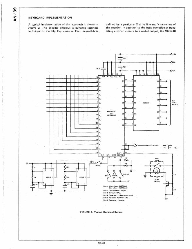
A typical implementation of this approach is shown in Figure 2. The encoder employs a dynamic scanning technique to identify key closures. Each keyswitch is
defined by a particular X drive line and Y sense line of the encoder. In addition to the basic operation oftranslating a switch closure to a coded output, the MM5740
" ++ 7
JJk LM555 3r-
fi =r='P'lJ-t ~
2V
-=k'M -I
G
*'M "
NO
,·"t 17 15 2 18 32 T, T, T'2 2 J 24 2J
12 X. ••• OE Vll VGG v~
11 X2 r£.-..!! B1 AB
10 ~ X, B2 Al
9 X, B]~A6
• X.
B4~A5 7 X,
5 X, Et9~A4
5 x. 85~A3
, x. MM5740AAC OR B6~A2" 22 MM5741lAAD
¥"
23 Y,1 B7~Al
24 Y2 1:l8~AO 25
Y,
26 Y4
Z7 Y<
26 Vs
'" Y,
~ os 30
Y, 14 osc
31 V9 SHIfT lK 20 eLK RPT SHIFT CONTROL
~" 21 " '"
1 10 Hl
-W- ~~ '50
S61lk . .t 7 H~' R
CONTROL SHIfT SHIFT
5IJOk LM!)S5 31"-
f 1 y "v
T"'~ Note 1: N·key tollover-MM5740AAC I·kev follover-MM574l1AAU
Note 2: Clo'dI: -fTequency'" 100 kHl.
Note 3: Scan cycie"'900!,;
Note 4: Repeat late = 10 characters Iler 5econd.
Note5: Ke bOUllce mask lime = 4 ms.
Nnw Ii: Datas1'obe" 1 OJISpillSl!.
FIGURE 2. Typical Keyboard System
10-28
B7
" " "
MM52.Uri
B3
B2
" BD
DATA STROBE
~
~ ~
~
~
~
~
~
KE CO
"" Y DE TPUTS
-=u= -10f1~
SHIFT LOCK r--l
"v--i--/ I (Q) i
~ ~~-~~ 12V 41!mA
CM2·7371
ENZ222
18k
I--
-lZY

provides all the functions necessary for modern keyboard system design. This includes all the logic necessary for key validation, 2·key or N·key rollover, bounce masking, mode selection and strobe generation. Table I illustrates the relationship between keyswitch matrix position, key mode and the binary coded outputs of the MM5740 AAC or AAD encoder. The AAC version provides for N-key rollover while the AAD is a 2-key rollover encoder. Since there are nine X lines, ten Y lines and four modes, 360 nine-bit codes are possible.
In the general application using 90 four mode keys, a 4k PROM (MM5204) should be used. If less than 64 fourmode keys are all that is required, a 2k PROM (MM5203) may be substituted. In this case, the most significant bit (B 1) from the encoder is dropped and Table I addresses would go from 0-255. When programming
the PROM, it should be noted that the MM5740 uses a bit paired coding system. Any particular key will have 5 common bits (8 1, 82, 83. 84, 89) and 4 variable bits (B5, B6, B7. B8) which may change when going from one mode to another. In addition, encoder coding is specified in terms of negative logic so that it may be necessary to complement positive logic PROM contents when ordering encoder masks.
By careful PC board layout, the encoder/PROM prototyping system can util ize the same PC board as the tinal system with the PROM removed. This can be accomplished by arranging the traces so that it is possible to provide jumpers from the encoder outputs to the PROM outputs. Utilizing this approach allows for a minimum of tooling, parts counts and quick turnaround time for new designs.
TABLE I. Encoder/PROM Mapping
KEY POSITION ADDRESSES KEY CODE OUTPUTS
MODE (ENCODER OUTPUT) (PROM CONTENTS)
X y B1 B283 84 89 85 86 B7 88 B7 86 85 B4 83 B2 81 80
1 1 Unshift 0 0 0 0 0 0 0 0 0
1 1 Shift 0 0 0 0 0 0 0 0 1
1 1 Control 0 0 0 0 0 0 0 1 0
1 1 Shift Control 0 0 0 0 0 0 a 1 1
1 2 Unshift ... 0 0 0 0 0 0 1 0 0
1 2 Shift 0 0 0 0 0 0 1 0 1 USER
1 2 Control 0 0 0 0 0 0 1 1 0 DEFINED
1 2 Shift Control 0 0 0 0 0 0 1 1 1 KEY
CODES
9 10 Unshift 1 0 1 1 0 0 1 0 0
9 10 . Shift 1 0 1 1 0 0 1 0 1
9 10 Control 1 0 1 1 0 0 1 1 0
9 10 Shift Control 1 0 1 1 0 0 1 1 1
,*En'coder outputs are listed in positive true logic notation.
10-29

2 <C MATRIX COMMON
ADDRESS B1 82 83
1 1 1 1 1 ,. 2 1 1 1 1 3 1 1 1 1 4 1 1 1 1 5 1 1 1 1 6 1 1 1 1 7 1 1 1 1 a 1 1 1 1 9 1 1 1 1 10 1 1 1 2 1 1 1 1 2 2 1 1 1 2 3 1 1 1 2 4 1 1 1 2 S 1 1 1 2 6 1 1 1 2 7 1 1 0 2 8 1 1 0 2 9 1 1 0 2 10 1 1 0 3 1 1 1 0 3 2 1 1 0 3 3 1 1 0 3 4 1 1 0 3 5 1 1 0 3 6 1 1 0 3 7 1 1 0 3 a 1 1 0 3 9 1 1 Q
3 10 1 1 0 4 1 1 1 0 4 2 1 1 0 4 3 1 0 1 4 4 1 0 1 4 5 1 0 1 4 6 1 0 1 4 7 1 0 1 4 8 1 0 1 4 9 1 0 1 4 10 1 0 1 5 1 1 0 1 ,S 2 1 0 1 5 3 1 0 1 5 4 1 0 1 5 5 1 0 1 5 6 1 0 1 5 7 1 0 1 5 3 1 0 1 5 9 1 0 0 5 10 1 0 0 6 1 1 0 0 6 2 1 0 0 6 3 1 0 0 6 4 1 0 0 6 5 1 0 0 6 6 1 0 0 6 7 1 0 0 6 8 1 0 0 6 9 1 0 0 6 10 1 0 0 7 1 1 0 0 7 2 1 0 0 7 3 1 a 0 7 4 1 0 0 7 5 0 1 1 7 6 0 1 1 7 7 0 1 1 7 8 0 1 1 7 9 0 1 1 7 10 0 1 1 8 1 0 1 1 8 2 0 1 1 8 3 0 1 1 8 4 0 1 1 8 5 0 1 1 8 6 0 1 1 8 7 0 1 1 8 8 0 1 1 8 9 0 1 1 8 10 0 1 1 9 1 0 1 0 9 2 0 1 0 9 3 0 1 0 9 4 0 1 0 9 5 0 1 0 9 6 0 1 0 9 7 0 1 0 9 B 0 1 0 9 9 0 1 0 9 10 0 1 0
ItNEGATIVE LOGIC NOTATION "1
B4 B9 BS
1 1 1 1 1 1 1 1 0 1 1 0 1 0 1 1 0 1 1 0 0 1 0 0 0 1 1 0 1 1 0 1 0 0 1 0 Q 0 1 0 0 1 0 0 0 0 0 0 1 1 1 1 1 1 1 1 0 1 1 0 1 0 1 1 0 1 1 0 0 1 0 0 0 1 1 0 1 1 0 1 0 0 1 0 0 0 1 0 0 1 0 0 0 0 0 0 1 1 1 1 1 1 1 1 0 1 1 0 1 0 1 ,. 0 1 1 0 0 1 0 0 0 1 1 0 1 1 0 1 0 0 1 0 0 0 1 0 0 1 0 0 0 0 0 0 1 1 1 1 1 1 1 1 0 1 1 0 1 0 1 1 0 1 1 0 0 1 0 0 0 1 1 0 1 1 0 1 0 0 1 0 0 0 1 0 0 1 0 0 0 0 0 0 1 1 1 1 1 1 1 1 0 1 1 0 1 0 1 1 0 1 1 0 0 1 0 0 0 1 1 0 1 1 0 1 0 a 1 0 0 0 1 0 0 1 a 0 0 a 0 a 1 1 1
·1 1 1 1 1 a 1 1 0 1 0 1 1 0 1 1 0 0 1 0 0 0 1 1 0 1 1
"0" = ..
TABLE II. Truth Table MM5740/AAC or MM5740/AAD
UNSHIFT SHIFt
86 87 8a ~5 86 B7 8a
1 1 1 1 1 1 0 0 1 1 1 0 1 0 1 1 1 0 1 1 0 0 1 1 0 0 1 0 1 1 1 1 1 1 0 0 1 1 1 0 1 0 1 1 1 0 1 1 0 0 1 1 0 0 1 0 1 1 1 1 1 1 0 0 1 1 1 0 1 0 1 1 1 0 1 1 0 0 1 1 0 0 1 0 1 1 1 1 1 1 0 0 1 1 1 0 1 0 1 1 1 0 1 1 0 0 1 1 0 0 1 0 1 1 1 1 ·1 1 0 0 1 1 1 0 1 0 1 1 1 0 1 1 0 0 1 1 0 0 1 0 1 1 1 1 1 1 0 0 1 1 1 0 1 0 1 1 1 0 1 1 0 0 1 1 a 0 1 0 1 1 1 1 1 1 0 Q 1 1 1 0 1 0 1 1 1 0 1 1 0 0 1 1 0 0 1 0 1 1 1 1 1 1 0 0 1 1 1 0 1 6 1 1 1 a 1 1 0 0 1 1 0 0 1 0 1 1 1 1 1 1 0 0 1 1 1 0 1 0 1 1 1 0 1 1 0 0 1 1 0 0 1 0 1 1 1 1 1 1 0 0 1 1 1 0 1 0 1 1 1 0 1 1 0 0 1 1 0 0 1 0 1 1 1 1 1 1 0 0 1 1 1 0 1 0 1 1 1 0 1 1 0 0 1 1 0 0 1 0 1 1 1 1 1 1 0 0 1 1 1 0 1 0 1 1 1 0 1 1 0 0 1 1 0 0 1 0 1 1 1 1 1 1 0 0 1 1 1 0 1 0 1 1 1 0 1 1 0 0 1 1 0 0 1 a 1 1 1 1 1 1 0 0 1 1 1 0 1 0 1 1 1 0 1 1 0 0 1 1 0 0 1 0 1 1 1 1 1 1 0 0 1 1 1 0 1 0 1 1 1 0 1 1 0 0 1 1 0 0 1 0 1 1 1 1 1 1 a 0 1 1 1 0 1 0 1 1 1 0 1 1 0 0 1 1 0 0 1 0 1 1 1 1 1 1 0 0 1 1 1 0 1 0 1 1 1 0 1 1 0 0 1 1 0 0 1 0 1 1 1 1 1 1 0 0 1 1 1 0 1 0 1 1 1 0 1 1 0 0 1 1 0 0 1 0 1 1 1 1 1 1 0 0 1 1 1 a 1 0 1 1 1 a 1 1 0 a 1 1 a a 1 0 1 1 1 1 1 1 0 0 1 1 1 0 1 0 1 1 1 0 1 1 0 0 1 1 0 0 1 0 1 1 1 1 1 1 0 n 1 1 1 a 1 0 1 1 1 0 1 1 0 0 1 1 0 0 1 0 1 1 1 1 1 1 0 0 1 1 1 0 1 0 1 1 1 0 1 1 0
0 1 1 0 0 1 0 1 1 1 1 1 1 0 0 1 1 1 0 1 0
BS
1 1 0 0 1 1 0 0 1 1 0 0 1 1 0 0 1 1 0 0 1 1 0 0 1 1 0 0 1 1 0 0 1 1 0 0 1 1 0 0 1 1 0 0 1 1 0 0 ., 1 0 0 1 1 0 0 1 1 0 0 1 1 0 0 1 1 0 0 1 1 0 0 1 1 0 0 1 1 0 0 1 1 0 0 1 1 0 0 1 1
CONTROL SHIFT CONTROL
SG B7 B8 85 B6 B7 so
1 0 1 1 1 0 0 0 0 1 1 0 0 0 1 0 1 0 1 0 0 0 0 1 0 0 0 0 1 0 1 1 1 0 0 0 o· 1 1 0 0 0 1 0 1 0 1 0 0 0 0 1 0 0 0 0 1 0 1 1 1 0 0 0 0 1 1 0 0 0 1 0 1 0 1 0 0 0 0 1 0 0 0 0 1 0 1 1 1 0 0 0 0 1 1 0 0 0 1 0 1 0 1 0 0 0 0 1 0 0 0 0 1 0 1 1 1 a 0 0 0 1 1 0 0 0 1 0 1 0 1 0 0 0 0 1 0 0 0 0 1 0 1 1 1 0 0 0 0 1 1 0 0 0 1 0 1 0 1 0 0 0 0 1 a 0 a 0 1 0 1 1 1 0 0 0 0 1 1 0 a 0 1 0 1 0 1 0 0 0 0 1 0 0 0 0 1 0 1 1 1 0 0 0 0 1 1 0 Q 0 1 0 1 0 1· 0 0 0 0 1 0 0 0 0 1 0 1 1 1 0 0 0 0 1 1 0 0 0 1 0 1 0 1 0 0 0 0 1 0 0 0 0 1 0 1 1 1 0 0 0 0 1 1 0 0 0 1 0 1 0 1 0 0 0 0 1 0 0 0 0 1 0 1 1 1 0 0 0 0 1 1 0 0 0 1 0 1 0 1 0 0 0 0 1 0 0 0 0 1 0 1 1 1 0 0 0 0 1 1 0 0 0 1 0 1 0 1 0 0 0 0 1 0 0 0 0 1 0 1 1 1 0 0 0 0 1 1 0 0 0 1 0 1 0 1 0 0 0 0 1 0 0 0 0 1 0 1 1 1 0 0 0 0 1 1 0 0 0 1 0 1 0 1 0 0 0 0 1 0 0 0 0 1 0 1 1 1 0 0 0 0 1 1 0 0 0 1 0 1 0 1 0 0 0 0 1 a 0 a 0 1 0 1 1 1 a a 0 0 1 1 0 0 0 1 0 1 0 1 0 a 0 0 1 0 0 0 0 1 0 1 1 1 0 a 0 0 1 1 0 0 0 1 0 1 0 1 0 0 0 0 1 0 0 0 0 1 0 1 1 1 0 0 0 0 1 1 0 a 0 1 0 1 a 1 a 0 0 0 1 a 0 a 0 1 0 1 1 1 a 0 0 0 1 1 0 a 0 1 0 1 0 1 a 0 a 0 1 0 0 0 0 1 0 1 1 1 0 0 0 0 1 , 0 0 0 1 0 1 a 1 a 0 0 0 1 a 0 0 0 1 0 1 1 1 0 0 0 0 1 1 0 0 0 1 0 1 0 1 0 0 0 0 1 0 0 0 0 1 0 1 1 1 a 0 0 0 1 1 0 0 0 1 0 1 a 1 o· 0 0 0 1 0 0 a 0 1 0 1 1 1 0 0 0 0 1 1 0 0 0