kg 102 - mike granby's website€¦ · · 2016-10-26revision 7 creates a new stand-alone...
TRANSCRIPT
MAINTENANCE MANUAL
KG 102DIRECTIONAL GYRO
MANUAL NUMBER 006-15622-0007REVISION 7 MARCH, 2002

WARNINGPrior to the export of this document, review for export license requirement is needed.
COPYRIGHT NOTICE
©1975-2002 Honeywell International Inc.
Reproduction of this publication or any portion thereof by any means without the express written permission of Honeywell is prohibited. For further information contact the manager, Technical Publications, Honeywell, One Technology Center, 23500 West 105th Street Olathe KS 66061 telephone: (913) 712-0400.

BENDIX/KING KG 102
Rev 7, March/2002 15622M07.JA Page RH-1
REVISION HISTORY
KG 102 Maintenance Manual
Part Number: 006-15622-XXXX
For each revision, add, delete, or replace pages as indicated.
REVISION No. 7, March/2002
Revision 7 creates a new stand-alone manual for the KG 102 which was extracted from revision 6 of the KCS 55/55A maintenance manual, (P/N 006-05111-0006). Any revisions to the KG 102, beginning with revision 7, will not be a part of the KCS 55/55A manual.
ITEM ACTION
All pages Full Reprint, new manual

BENDIX/KING KG 102
Page RH-2 15622M07.JA Rev 7, March/2002
THIS PAGE IS RESERVED

BENDIX/KING KG 102
Rev 7, March/2002 15622M07.JA Page i
TABLE OF CONTENTS
SECTION IVTHEORY OF OPERATION
PARAGRAPH PAGE
4.1 General 4-1
4.2 Power Supply 4-1
4.3 Heading Display Drive Circuit 4-2
4.3.1 Heading Display Drive Detail Operation 4-3
4.3.2 Auto-Manual Slaving Circuitry-Detail Operation 4-12
SECTION VMAINTENANCE
PARAGRAPH PAGE
5.1 Introduction 5-1
5.2 Test and Alignment 5-1
5.2.1 General Requirements 5-1
5.2.2 Power, Signal Test Sources, and Test Equipment 5-1
5.2.3 Test Equipment 5-2
5.2.4 Test Requirements 5-2
5.2.5 P.C. Board Test 5-2
5.2.6 Gyro Test 5-4
5.2.7 Final Test Procedure 5-5
5.3 General Overhaul 5-15
5.3.1 Visual Inspection 5-15
5.3.2 Cleaning 5-16
5.3.3 Repair 5-21
5.4 Disassembly/Assembly Procedures 5-25
5.4.1 Electronics Assembly Removal 5-26
5.5 Gyro Overhaul 5-26
5.5.1 Inspection 5-26
5.5.2 Gyro Cleaning 5-27
5.5.3 Gyro Disassembly/Assembly 5-29
BENDIX/KING KG 102
Page ii 15622M07.JA Rev 7, March/2002
SECTION VMAINTENANCE (cont).
PARAGRAPH PAGE
5.6 Gyro Troubleshooting 5-53
5.6.1 Troubleshooting Flowchart 5-53
5.6.2 Troubleshooting Gyro 5-53
SECTION VIILLUSTRATED PARTS LIST
PARAGRAPH PAGE
6.1 General 6-1
6.2 Revision Service 6-1
6.3 List of Abbreviations 6-1
6.4 Sample Parts List 6-3
6.5 KG102 Final Assembly 6-5
6.6 KG102 Electronics Assembly 6-11
6.7 KG102 Power Supply Board Assembly 6-15
6.8 KG102 Logic Board Assembly 6-29
6.9 KG102 Cable Assembly 6-45
6.10 KG102A Digital Filter Board Assembly 6-51
6.11 R.C. Allen Gyro Information 6-53
LIST OF ILLUSTRATIONS
FIGURE PAGE
4-1 Flux Valve Excitation Waveform 4-2
4-2 KG 102 Gyro Output Waveforms 4-2
4-3 Gyro-to-Motor Logic Block Diagram 4-3
4-4 KI 525 Compass Card Display 4-4
4-5 Filter Circuit Schematic/Time Relationship 4-5
4-6 CW Heading Rotation Waveform Sequence 4-8
4-7 CCW Heading Rotation Waveform Sequence 4-9
4-8 CW Heading Rotation Waveform Reconstruction Sequence 4-10
4-9 CCW Heading Rotation Waveform Reconstruction Sequence 4-11
4-10 Auto-Manual Pulse Generator Sequence 4-15

BENDIX/KING KG 102
Rev 7, March/2002 15622M07.JA Page iii
LIST OF ILLUSTRATIONS (cont).
FIGURE PAGE
5-1 Electrical Directional Gyro Assembly Exploded View 5-32
5-2 Axis Assembly Showing Balancing Adjustment Points 5-41
5-3 Wiring Diagram for Electrical Directional Gyro Assembly 5-44
5-4 KG 102 Troubleshooting Flow Chart 5-53
5-5 Schematic Diagram with Suggested Impedance Load 5-55
5-6 Oscilloscope Pattern for Switching Outputs at 30Deg/Sec CW Rotation 5-56
5-7 Gyro Circuit Board Schematic 5-65
5-8 KG 102 Test Circuit 5-67
6-1 Sample Parts List 6-3
6-2 KG 102 Final Assembly 6-7
6-3 KG 102 Electronics Assembly 6-13
6-4 KG 102 Power Supply Board Assembly 6-17
6-5 KG 102 Power Supply Schematic 6-23
6-6 KG 102 Logic Board Assembly 6-31
6-7 KG 102 Logic Assembly Schematic 6-39
6-8 KG 102 Cable Assembly 6-47
6-9 Remote Gyro Assembly 6-57

BENDIX/KING KG 102
Page iv 15622M07.JA Rev 7, March/2002
THIS PAGE IS RESERVED

BENDIX/KING KG 102
Rev 7, March/2002 15622M07.JA Page 4-1
SECTION IVTHEORY OF OPERATION
4.1 GENERALThe KG 102 gyro forms the heart of the KCS 55 compass system in that it supplies the basic head-ing reference. In addition, it converts the aircraft power whether +14 or +28VDC to the various volt-age levels required by the other system units as well as for the gyro itself. It converts the flux valve slaving error to digital pulses to be summed with the digital gyro signal, and is then changed to the proper digital format to operate the stepper motor compass card drive in the KI 525. Finally, it ac-cepts the auto and manual slaving commands from the KA 51 switch and meter unit to control speed and direction of the slaving activity.
4.2 POWER SUPPLYSystem power for the KCS 55 compass is supplied by the KG 102 gyro, and is generated solely from the +14VDC or +28VDC aircraft power. From this source, the following internal supplies are generated: 26VAC, 400Hz for the gyro spin motor and flux valve excitation; ±15VDC regulated supply for the linear circuitry in the system; +15VDC unregulated voltage for the KI 525 stepper motor drive, the glideslope pointer and power flag current; and +5VDC regulated supply for the system logic circuitry and LED drive current in the KI 525.Input power enters the KG 102 through pin e and is filtered by the LC network consisting of ca-pacitors C225, C226 and inductor L201. A 6.0 volt regulator, I221, supplies power for 800 Hz os-cillator I220. This signal is required to demodulate the flux valve signal in the auto-slave input cir-cuit to be described later, and also to drive the flip-flop consisting of transistors Q210, Q211, and associated parts. The flip-flop performs the function of a frequency divider, supplying 400Hz wave-forms that are 180 degrees out of phase to transistors Q212 and Q213. Diode CR216 and capac-itor C228 steer the 800Hz signal to Q210 shutting it off on the negative going transition of the 800Hz waveform when Q210 stops conducting, current flows through resistors R265 and R269 to the base of Q211, causing it to start conducting. This removes the base drive to Q210 allowing the circuit to stabilize with Q210 off and Q211 on. When the next negative going transition of the 800Hz waveform appears, it is steered through capacitor C229 and diode CR217 to the base of Q211. This negative pulse deprives Q211 of base current causing it to shut off. Current begins to flow through resistors R266 and R270 to the base of Q210, turning that transistor on. In this way, a complete cycle of the flip-flop operation is achieved for every two cycles of the 800Hz input waveform resulting in a 400Hz drive signal to the inverter transformer drive transistors.Transistor pairs Q213-Q215 and Q212-214 form darlington pairs that switch alternate ends of in-verter transformer T201 to ground at 400Hz in response to the flip-flop output signal. Switch S201 effectively changes the turns ratio of the transformer allowing operation on +14VDC or +28VDC. The secondary windings of T201 develop the four individual supplies for the system operation.First of all, a floated winding is used to generate the 26VAC necessary to drive the gyro spin motor and to excite the flux valve. A modification of the 26VAC waveform is made prior to excitation of the flux valve. The circuitry that performs this modification will be explained at the end of this sec-tion.Secondly, a center tapped winding is used to generate the ± 15VDC regulated supply for the linear circuitry in the system. A conventional full wave bridge rectifier is used to convert the 400Hz wave-form to DC and capacitors C230 and C231 filter this voltage prior to entering the zener regulator circuit. Positive current passes through resistor R275 to zener CR219 across which is developed the reference voltage of 16VDC.

BENDIX/KING KG 102
Page 4-2 15622M07.JA Rev 7, March/2002
Approximately ONE volt is dropped across the base to emitter junctions of darlington connected transistors Q220 and Q221 resulting in +15VDC appearing across output filter capacitor C233. Negative current passes through resistor R276 to zener CR220 developing the reference voltage for transistors Q218 and Q219. The output from this darlington connected pair appears across ca-pacitor C234 as -15VDC.The third secondary winding is used to generate the +15VDC unregulated supply and the +5VDC regulated logic supply. Here again, a conventional full wave bridge rectifier is used to convert the 400Hz waveform to DC, and capacitor C232 filters this voltage producing the unregulated +15VDC supply. From here, current flows through resistor R277 and zener CR218 where the ref-erence 6.2VDC is developed. Approximately 1.2VDC is dropped across the base to emitter junc-tions of darlington connected transistors Q216 and Q217 resulting in +5VDC appearing across ca-pacitor C235.Individual ground lines have been established for the various circuits including signal ground for the linear circuitry, digital ground for the logic, unregulated ground for the stepper motor and power flag, and power ground for the input +14VDC or +28VDC aircraft ground.As mentioned above, a modification is made to the 26VAC waveform prior to exciting the flux valve. This modification consists of rounding the edges of the square wave to achieve an enhance-ment of the flux valve output. An RC network consisting of resistors R152 and R153 along with capacitors C137 and C138 is used for this purpose and is shown in Figure 4-1. This circuit is lo-cated on the logic board.
FIGURE 4-1 FLUX VALVE EXCITATION WAVEFORM
4.3 HEADING DISPLAY DRIVE CIRCUITHeading information is obtained from the directional gyro mounted on the KG 102 chassis and is in the form of two output waveforms that are 90 degrees out of phase with each other as shown in Figure 4-2.
FIGURE 4-2 KG 102 GYRO OUTPUT WAVEFORMS

BENDIX/KING KG 102
Rev 7, March/2002 15622M07.JA Page 4-3
A signal transition occurs at pin D or E every quarter degree of heading change and is phased such that pin E leads pin D for CW rotation of the gyro (increasing heading). Since these signals are generated by op-amps in the gyro and are switching between ±15VDC, a limiting circuit is re-quired to reduce the voltage to TTL logic levels.Resistor R301 and R302 along with zener diodes CR301 and CR302 limit the input voltage on pins D and E to +4. 3VDC and -0.6VDC. Exclusive OR Gate I302 and Flip Flop I301 form a digital filter designed to delay the input transitions by one step to prevent noise from affecting the compass display card in the KI 525 (see figure 4-5). NAND gates I101 A and B along with INVERTERS I102 C and D plus resistors R101 and R102 shape the gyro input waveforms prior to exciting the four one-shot circuits to be described below. A block diagram showing the operation of this part of the circuit in general terms will be given (Figure 4-3).
FIGURE 4-3 GYRO-TO-MOTOR LOGIC BLOCK DIAGRAM
Each transition of the filtered input waveform excites one of the four one-shots resulting in a 0.18ms pulse. This pulse is connected to a summation gate along with the outputs of the other three one-shots. There are actually two of these summation gates to which the four one-shots are connected, but only one transmits pulses at a time. This selection is made as a function of gyro rotation direction. From these summation gates, the pulses are connected to the output of the KG 102 for use as a Yaw rate signal. In addition to going to the output, the pulses go to a second pair of summation gates where similar pulses from the slaving circuit are added to the pulse train. Here again, the desired direction of slaving activity determines which summing gate the pulses enter through.From here, the pulses enter a two-phase-state generator. This generator reconstructs the wave-form required for the stepper motor operation in the KI 525 indicator which runs the heading dis-play card. This waveform has the same format as the gyro input waveform except that it now in-cludes the slaving pulses necessary to keep the display card aligned with the magnetic flux valve.
4.3.1 HEADING DISPLAY DRIVE DETAIL OPERATION
As explained above, exclusive OR Gate 1302 and Flip Flop I301 form the digital filter circuit. Gates I302A and D serve to shape the input signals by increasing the switching speed of those signals prior to exciting flip flops I301 A and B. A mechanical analogy will be used to describe the basic operation of the filter, figure 4-4.

BENDIX/KING KG 102
Page 4-4 15622M07.JA Rev 7, March/2002
FIGURE 4-4 KI 525 COMPASS CARD DISPLAY
The KG 102 gyro output signal is represented by the car labeled "X" above. This car moves along the upper rail in one-quarter degree increments represented by the letter designations A, B, C, etc. The car labeled "Y" is pulled along the lower rail by a cable connected to Car "X". As seen in figure 4-4, "Y" trails behind "X" by a quarter degree increment. When "X" reverses direction, Figure 4-4, B, the cable goes slack until it reaches position B, Figure 4-4, C, thus causing no motion of car Y. In this manner, oscillatory motion of Car "X" that does not exceed one half degree will produce no motion of Car "Y". This feature is the primary objective of the filter circuit; that is to prevent the compass card in the KI 525 indicator from responding to vibration induced output from the KG 102 gyro.Figure 4-5 shows the schematic and the time relationship between the waveforms at various points in the filter circuit.Starting at period A with voltage levels as shown, three output transitions from the KG 102 gyro will be shown along with the resulting filter output waveforms that drive the KI 525 Compass Card. Exclusive OR Gates I302 B and C provide the clocking signals to Flip Flops I301 A and B. These Flip Flops transfer the data at the "D" inputs to the "Q" outputs on the positive going transition of the clock signal.At period B, shaping Gate I302A switches from a logic 1 to a logic 0. This, together with the logic 1 at the Q output of I301B pin 9 (opposite of Q output of 1301B pin 8) produces a logic 1 at pin 6 of Gate I302B. Since this represents a positive going transition at the clock input of Flip Flop I301A, the logic 1 signal at the "D" input will be transferred to the Q output pin 5. The Q output, pin 6 will switch to a logic 0 as shown in Figure 4-5. As a result of this transition, exclusive OR Gate I302C switches to a logic 0 in preparation for the input transition C which will cause it to switch back to a logic 1, providing the positive going clock transitions for Flip Flop I301B. When input tran-sition C does occur, the logic 0 at I302A is transferred to I301B pin 9. The Q output pin 8 switches to a logic 1 at the same time as shown in Figure 4-5. At input transition D, input Gate I302A switch-es to a logic 1, causing output I301A pin 6 to also switch high. It is clear that each input transition produces an output on the opposite channel. In a sense, the output is always one step behind the input as was described in the mechanical analogy Figure 4-4. At this point, we will reverse the direction of the gyro rotation and observe the similarity between the compass display and the anal-ogy used above.

BENDIX/KING KG 102
Rev 7, March/2002 15622M07.JA Page 4-5
FIGURE 4-5 FILTER CIRCUIT SCHEMATIC/TIME RELATIONSHIP

BENDIX/KING KG 102
Page 4-6 15622M07.JA Rev 7, March/2002
At period F in Figure 4-5, the output of Gate I302A switches to a logic 0. Since this gate also con-tributed the previous transition (Period D) we know a direction reversal has occurred because the two inputs alternate during periods of constant direction activity. This transition causes the output of Exclusive or I302B to transition to a logic 0. Since this represents a negative going clock signal to Flip Flop I301A, it does not change state. This is similar to the situation depicted in the analogy Figure 4-4, Condition B. At Period G, input Gate I302D switches to a logic 1 causing the clock sig-nal at I302C to transition to a logic 1 also. This will cause the logic 0 at the input to Flip Flop I301B to be transferred to the output, but the output U301B pin 9) is already a logic 0 (opposite of Q out-put I301B pin 8) so no change of state occurs. We have now reached the condition depicted in the analogy Figure 4-4, C. All of the "slack" has been taken up and any addition transitions in the same direction will produce corresponding motion of the compass card. This happens at Period H where the input transition at I302A causes a positive going clock signal at the output of I302B, transfer-ring the logic 1 at the input of Flip Flop I301A to the Q output. This also results in the logic 0 tran-sition at the Q output of I301A.The output of the filter is connected to NAND gates I101A and B and INVERTERS I102C and D shape the input gyro waveforms in preparation of exciting the four one-shots. It will be noticed that outputs are obtained from both sides of the inverter in the shaping circuit, This creates four wave-forms, each pair being 180 degrees out of phase with each other and 90 degrees out of phase with the other pair. It is further noticed that each of these four outputs excite one and only one of the one-shots. Each output also controls two gates that steer the one-shot pulses to the correct heading rotation line, i.e. CW rotation only permits pulses to appear at the output of I106B and at I106A for CCW rotation. Figure 4-6 (top) illustrates the four waveforms as they appear on either side of inverters I102C and D. This illustration will be used to trace the operation of the steering circuit through a CW and a CCW cycle of operation. The one-shots are triggered by the negative going transition of the input originating at pin D or E of the connector and is steered by the state of the other input. In this way, the steering signal has long since stabilized by the time the one-shot pulse arrives, avoiding race conditions arising from lags in the switching circuitry.A typical CW cycle may begin with a negative transition at the output of I102C which result9 in a one-shot pulse at I102F as shown. This pulse is connected to I104A and B, however, 1104B is shut off by the low state of I102D, thus only I104A transmits the pulse. This output is connected to I106B and thence to the output on the YAW CW line, Logic gate I101B is next to transmit a neg-ative transition. This transition results in a pulse at the output of I103A which is connected to gates I105C and D. As before, only one of these can transmit the pulse. Since I101A is in the high logic state, it will allow the pulse to pass through I105D to which it is connected. It will immediately be noted that I105D is also summed into I106B where it is tied to the output YAW CW line. Next in line is I101A resulting in a pulse at I102A and thence at I104C resulting from the logic high at I102D. This pulse is also connected to I106B. The last pulse of this cycle results from the negative transition at I102D. A pulse occurs at I103F and then at I105B where it is transmitted to I106B. This sequence will continue as long as the gyro is rotated in a CW direction and the pulses will only appear at pin s corresponding to CW rotation of the heading gyro.Counter clockwise rotation of the heading gyro results in a similar train of pulses on the YAW CCW line at pin f. This sequence is shown in Figure 4-7 beginning on the right side (Line F) and pro-ceeding right to left.Beginning with the negative transition at 1102D and following the pulse, generated at I103F to I105A and B, it is clear that only I105A will transmit due to the logic high at I101A. I105A is con-nected to I106A which sums all of the CCW pulses and transmits them to pin f on the YAW CCW line. Next to switch is I101A resulting in a pulse at I102A. The logic high at I101B steers pulse through 1104D and thence to I106A. Following I101A is I101B resulting in a pulse at I103A. The logic high at I102C directs the pulse to I105C and thence to I106A. Lastly, the transition at I102C results in a pulse at I102F and steered through I104B by the logic high at I102D to I106A.

BENDIX/KING KG 102
Rev 7, March/2002 15622M07.JA Page 4-7
From I106A and B, the CCW and CW pulses go to gates I107A and D respectively where they are summed with the CCW and CW slaving pulses. The origin of these pulses will be explained later. Following the summation of the gyro and slaving pulses, a reconstruction process begins whereby the original gyro output waveforms, plus the slaving transitions are formed from the CCW and CW pulses appearing at I107A and D.Forming the heart of the reconstruction circuitry, are two D-type flip-flops, the output of which take on the value of the input (pins 2 and 12) at the end of the clock pulse (pins 3 and 11). These clock pulses are nothing more than the summation of the CW and CCW pulses at I107A and D summed together at I108C. Figures 4-4 and 4-5 trace a CW and CCW cycle through the reconstruction pro-cess resulting in a set of waveforms that have a striking resemblance to those appearing at pins D and E of the gyro input connector.A CW reconstruction cycle shown in Figure 4-8 begins with both flip-flops, I110A (5) and B (9) in the high logic state, (line A). Since the CW pulses only appear at the output of I107D, a positive transition will occur at I101D when the first CW pulse arrives. This logic ONE state along with the steady state logic ZERO at I101C, forcing I101D to latch up in the logic ONE condition until a CCW pulse occurs. This signal enables gates I108A and B, while inhibiting gates I109 B and C due to the inversion of the logic ONE signal by inverter I103D. Since the output FF I110A pin 5 is high, it along with the logic ONE at I110D, will produce the ZERO at 1108A, and thence a logic ONE at I109A to the input of I110B. As mentioned above, the FF will take on the value of the input at the end of the clock pulse, but since the output I110B is already high, no change will occur. Unlike the input of I108A which is connected to the Q output of I110A, its counterpart, I108B, has its input connected to the Q output of I110B. Since the Q output is of the opposite polarity of the Q output, a logic ZERO appears at the input of I108B producing a logic ONE at the output and thence a logic ZERO at I109D which is tied to the input of I110A. At the end of the next clock pulse, this logic ZERO will be transferred to the output of I110A as shown in Figure 4-8 one clock pulse after time A. The Q output of each FF will always be the opposite of the Q output of that flip-flop. Now that I110A (5) has switched to a logic ZERO, I108A will go high, followed by a logic ZERO at I109A and thence to I110B. This zero will be transferred to the output of I110B at the end of the next clock pulse as shown at time B in Figure 4-8. This results in a logic ONE at the input of I108B which passes through I109D to I110A as a logic ONE. At the end of the next clock pulse, I110A (5) will switch high and provide a logic ONE at the input to I110B. In this manner, the flip-flops switch ON and OFF in an alternate fashion resulting in the reproduction of the two-phase state signal required by the KI 525 stepper motor.Reconstruction of the CCW cycle is essentially the same as the CW sequence except that gates I109B and C are now enabled by I103D and I108A and B are inhibited by I101D. When the CCW pulses appear at I107A, they cause I101C and D to latch up in the opposite state where I101D is a logic ZERO. This state reversal simply connects I110A (6) instead of I110A (5) to I110B, and 1110B (9) instead of I110B (8) to I110A. The sequence can be reconstructed by following the waveforms shown in Figure 4-9, going from right to left.In addition to providing steering data for the reconstruction circuitry, the flip-flops also provide drive current for the four stepper motor switching transistors Q101, 102, 103 and 104. These tran-sistors supply the ground return for alternate pairs of motor coils in response to the flip-flop com-mands. Diodes CR129, 130, 131, and 132 are connected across the motor coils to eliminate the large reverse voltage that would occur when the coils are opened.

BENDIX/KING KG 102
Page 4-8 15622M07.JA Rev 7, March/2002
FIGURE 4-6 CW HEADING ROTATION WAVEFORM SEQUENCE

BENDIX/KING KG 102
Rev 7, March/2002 15622M07.JA Page 4-9
FIGURE 4-7 CCW HEADING ROTATION WAVEFORM SEQUENCE

BENDIX/KING KG 102
Page 4-10 15622M07.JA Rev 7, March/2002
FIGURE 4-8 CW HEADING ROTATION WAVEFORM RECONSTRUCTION SEQUENCE

BENDIX/KING KG 102
Rev 7, March/2002 15622M07.JA Page 4-11
FIGURE 4-9 CCW HEADING ROTATION WAVEFORM RECONSTRUCTION SEQUENCE

BENDIX/KING KG 102
Page 4-12 15622M07.JA Rev 7, March/2002
4.3.2 AUTO-MANUAL SLAVING CIRCUITRY-DETAIL OPERATION
Slaving pulses that sum with the gyro signals at I107A and D, originate at I115, an integrated timer circuit. This timer operates as a pulse generator only during auto or manual slaving operation, and at a frequency determined by the auto-manual slave command status. During periods of manual slave operation, the pulses occur at approximately 24Hz, and since each pulse represents a quar-ter degree heading change on the KI 525 indicator, this represents a six degree per second man-ual slaving rate. During auto slave operation, the pulses occur at approximately 14Hz during the first two minutes and at one pulse every five seconds thereafter.Timer circuit I115 transmits a logic ONE signal from pin 3 whenever a negative pulse occurs at pin 2, Figure 4-10. Coincidently, a shorting switch is removed from across the timing capacitor, allow-ing it to begin charging up. When the capacitor voltage reaches 66 percent of the supply voltage, the shorting switch is again placed across the capacitor, discharging it and forcing pin 3 to a logic ZERO. This negative transition if inverted by I112E from which it goes to a one-shot generator, to be explained later, and gate I108D which provides the timer inhibit when no slaving commands are present. From I108D, the negative transition is coupled through capacitor C113 and R117 to inverter I112A. At this point, a phenomenon occurs which is characteristic of the TTL logic devices with which the KG 102 is designed. When the negative transition that is coupled through C113 reaches the input of I112A, the inverter (I112A) reacts as if a normal logic ZERO has been applied to the input, and transmits a logic ONE. After approximately 0.5ms, however, when the capacitor has fully charged and current is no longer flowing into the capacitor plates from I112A, there is insufficient current flowing through resistor R117 to hold the input of I112A at a logic ZERO. This causes the output to switch from a logic ONE back to a logic ZERO even though 1108D is still at a logic ZERO. In this manner, a positive pulse of approximately 0.5ms is generated at the output of I112A whenever a negative transition occurs at I108D. This pulse is sharpened up by the invert-ers I112B and C where the positive pulse, still 0.5ms long again appears. At this point the pulse passes through another resistor capacitor circuit consisting of R116 and C114. C145 is used to suppress high frequency noise. Prior to the positive pulse at I112C, the output of I112F is at a logic ZERO. even though I112C is still at a logic ZERO, because of the insufficient current through R116 as explained before. For this reason, when the leading positive-going edge of the pulse occurs, it is simply coupled through C114 until the capacitor is full charged, but no change in the output oc-curs because it is already at a logic ZERO.When the trailing negative-going edge occurs, however, it is coupled through C114 is fully charged and the output of I112F again returns to a logic ONE. Approximately 2 microseconds after the fall-ing edge occurs, C114 is fully charged and the output of I112F again returns to a logic ZERO even though I112C is still at a logic ZERO. The end result of all this is a 2 usec pulse occurring at the trailing edge of a 0. 5msec pulse. From I112F, the pulse goes through I112D where it is inverted to become a 2 usec negative-going pulse and thence to pin 2 of timer circuit I115. Timer circuit I115 transmits a logic ONE signal from pin 3 whenever a negative pulse occurs at pin 2. The timing sequence is illustrated in Figure 4-10.As mentioned earlier, the output of I112E is also connected to a one-shot consisting of inverters I114A and B along with resistor B107 and capacitors C109, C110 and C143 which is a noise sup-pression capacitor. This one-shot is stimulated in the same manner as the previous capacitively coupled circuits were, in that only the negative transition will be coupled into the inverter gate I114A and thence to I114B. C110 provides positive feedback to I114A in order to shape and lengthen the pulse to 0.2ms. From I114B, this pulse goes to gates I107B and C which are the con-trol gates for the CW or CCW slave pulse input to the two-phase state generator circuitry.The control signals that determine through which of these two gates the slaving pulses will be transmitted are generated by the circuitry described as follows.

BENDIX/KING KG 102
Rev 7, March/2002 15622M07.JA Page 4-13
During manual slave operation, zero volts is present at pin c preventing Q107 from conducting. This allows current to flow through R118, R115 and CR105 to timing capacitor C112. In addition, the voltage at the collector of Q107 is sufficiently high to represent a logic ONE to I114E which transmits a logic ZERO to gates I113B and C, inhibiting them. Inputs I113D (13) and I113A (1) are connected to the clockwise and counter-clockwise manual slave switches, Q105 and Q106 re-spectively. When no slave command is present, pins j and n are at ground potential resulting in a logic ONE at the collectors of Q105 and Q106. This results in logic ZERO at I113A and D. These outputs are connected to I114D and C where logic ONES inhibit gates I107B and C preventing any pulses from entering the gyro circuit through I107A and D. In addition, the logic ZERO at I113A and D generate a logic ONE at I111A and a ZERO at I114F. This ZERO inhibits I108D, preventing timer circuit I115 from oscillating and producing slaving pulses. When the CW or CCW slave com-mand is activated, a logic ONE will appear at j or n respectively. This will cause Q105 or Q106 to turn on, supplying a logic ZERO to I113D or A respectively. The output of this gate will be a logic ONE which will be transmitted through I111A, I114F, to I108D where the timer inhibit will be re-moved. This allows the timer to generate slaving pulses at 24Hz appearing at I107B and C. The output at I113D or A will pass through I114C or D to the other input of I107C or B, where it will allow the slaving pulses to pass through and sum with the gyro pulses at I107D or A.When the auto-slave function is engaged, a logic ONE appears at c, turning on I116 and Q107.The output of I116 at pin 3 goes to a logic ONE and supplies timing current through CR106, R114 and C112 causing the timer I115 to generate slaving pulses at 14Hz. After approximately two min-utes, capacitor C111 will have charged through R112 to 66 percent of the supply voltage, and cause pin 3 of I116 to return to a logic ZERO. When this occurs, charging current no longer flows through CR106, but through R113, reducing the pulse frequency to one pulse every five seconds. A logic ZERO appearing at Q107 will generate a logic ONE at I114E and thence at the inputs of I113B and C removing the inhibit formerly present at these gates. The other input to gates I113B and C come from a phase detector connected to the magnetic flux valve. From the flux valve, the magnetic heading signal enters the KG 102 through pins v and w. This signal is a very low mag-nitude and somewhat distorted. Capacitor C120 shifts the phase of the 800 Hz flux valve signal to cause it to be in phase or out of phase with the reference 800Hz supplied from timer I220 in the power supply section (Section 4.2 above). Resistors R127, R128, R129 and R130; capacitors C118 and C119; and amplifier I118A form a second order filter designed to accentuate the 800Hz component of the input signal and greatly attenuate all other frequencies. From I118A, the wave-form passes to a demodulator or phase detector, consisting of switching FETS Q108 and Q109; Resistors R131, R132, R134, R138, and R139; capacitors C131, C122, C123 and C124; and am-plifier I118B. The 800Hz reference signal causes transistor Q122 to switch ON and OFF, supply-ing the gates of Q108 and Q109 through CR111 and CR112 with alternating +15VDC and ground. When Q109 is off, +15VDC forces Q108 and Q109 to shut off because of the reverse biased gate-drain junction. This allows one-half cycle of the signal current to pass through R131 and E132 to the inverting side (pin 6) of I118B. Since Q109 is OFF, no signal current will pass to the non-in-verting side of Q118B. During the next half-cycle of the 800Hz waveform, Q122 is conducting and grounds the gates of the two FETS. This allows signal current to pass through Q109 to the non-inverting side of I118B and to be shorted to ground through Q108 on the inverting side.The polarity of the signal current, however, will be opposite to what it was during the previous half-cycle and will generate the same polarity signal at the output of I118B. This polarity positive, neg-ative, or zero (zero in the case of no slaving error), will determine which of the slaving switches, I119A or I119B will turn on and allow CW or CCW slaving pulses to be summed with the gyro puls-es. Capacitors C121, C122, C123, and C124 filter the pulsating DC voltage at the output of I118B. This signal now represents the difference in magnetic direction as measured by the KMT 112 flux valve, and the magnetic heading as displayed on the KI 525 indicator and displays this difference on the slave meter connected to pin k through resistor R179 in the KA 51.
BENDIX/KING KG 102
Page 4-14 15622M07.JA Rev 7, March/2002
Besides operating the slave meter the DC signal also operates a slave switch consisting of ampli-fiers I119A and B along with the associated resistors. When the output of I118B is less than ap-proximately ±0.5VDC, both amplifiers, I119A and B will be biased full negative by the influence of the -15VDC supply through resistors R145 and R146 respectively. Resistor R147 and zener diode CR113, which will conduct in the forward biased mode when a negative voltage is applied, limits the input to gate I113B to -0.6VDC. Resistor diode combination R148 and CR114 perform the same function between amplifier I119B and gate I113C. This negative voltage corresponds to a logic ZERO at I113B and C and prevents a slave command from reaching I113A or D which serve as a sum point for the auto and manual slave commands. As the magnetic heading as sensed by the flux valve becomes larger than the heading displayed on the KI 525 due to drift in the direc-tional gyro, an 800Hz signal which is out of phase with the 800Hz reference signal from the KG 102 power supply appears at pin v. This signal results in a positive voltage at the output of I118B and causes I119B to switch from approximately -13VDC to approximately +14.5VDC. Resistor R148 and zener diode CR114 limit the voltage at the input to gate I113 to about 4. 5VDC. This results in a logic ZERO at the output of I113C and a logic ONE at I113D permitting slaving pulses to sum with the YAW CW pulses at I107D. These pulses, which represent a quarter of a degree of heading, occur at the ratio of one every five seconds. This computes out to an auto slave rate of three degrees a minute. When the displayed heading comes into conformance with the flux valve heading, I119B returns to -13VDC and the slaving pulses are discontinued. If the displayed heading becomes greater than the flux valve heading, an in-phase 800Hz signal appears at pin v and generates a negative voltage at the output of I118B. This causes I119 to switch to +14. 5 DC, removing the inhibit on I113B, and allowing slaving pulses to sum With the gyro YAW CCW pulses at I107A.

BENDIX/KING KG 102
Rev 7, March/2002 15622M07.JA Page 4-15
FIGURE 4-10 AUTO-MANUAL PULSE GENERATOR SEQUENCE

BENDIX/KING KG 102
Page 4-16 15622M07.JA Rev 7, March/2002
THIS PAGE IS RESERVED

BENDIX/KING KG 102
Rev 7, March/2002 15622M07.JA Page 5-1
SECTION VMAINTENANCE
5.1 INTRODUCTION This section deals with the testing, overhaul, and troubleshooting procedures for the KG 102 Di-rectional Gyro.
5.2 TEST AND ALIGNMENTThe following establishes the performance requirements that this unit must meet before it can be used as part of an operational system.
5.2.1 GENERAL REQUIREMENTS
Unless otherwise specified, all tests shall be conducted with the gyro in its normal operating posi-tion and at ambient room temperature (25 ±5 degrees C) and humidity not to exceed 80%.
5.2.1.1 ELECTRICAL
Output Signalsa. Two phase state signal to KI 525 stepper motor.b. CW and CCW yaw rate pulse frequency modulated signal.c. Slave meter drive signal.d. 26VAC 400Hz.e. 400Hz flux valve excitation.f. ±15VDC for KI 525.g. +5VDC for KI 525.h. +15VDC unregulated for KI 525.
5.2.1.2 ELECTRICAL
Input Signalsa. 800Hz flux valve signal.b. Auto-manual slave signal 0/+5.c. CW Manual slave signal 0/+5.d. CCW Manual slave signal 0/+5.e. +14/+28VDC power input.
5.2.1.3 MECHANICAL
Gyro photocell output accuracy. D to E waveforms 90 deg. ±40 degrees.
5.2.2 POWER, SIGNAL TEST SOURCES, AND TEST EQUIPMENT
5.2.2.1. POWER INPUT
a. +14VDC - 3. 0 ampb. +28VDC - 1. 5 amp
5.2.2.2 SIGNAL TEST CIRCUITS
Electronic test circuitry shown in Figure 5-8.

BENDIX/KING KG 102
Page 5-2 15622M07.JA Rev 7, March/2002
5.2.3 TEST EQUIPMENT
a. DC voltmeter - Similar to Hewlett-Packard, Model 412A.b. AC voltmeter - Similar to Ballantine Laboratories Inc., Model 300-G.c. Oscilloscope - Similar to Tektronix, Model 516.
5.2.4 TEST REQUIREMENTS
5.2.5 PC BOARD TEST
1. Connect the system as shown in Figure 5-8 with the casting removed from the elec-tronics assembly and all power switches OFF. Place the 14/28v switch on the KG 102 chassis to 14v and the GYRO/SIM switch to SIM.
2. Switch the 14VDC on and record the following voltages:a) Gyro Connector Pin A to B 26 ±3VACb) Gyro Connector Pin F +15 ±1VDCc) Gyro Connector Pin J -15 ± 1VDCd) Gyro Connector Pin C +5 ±0.5VDCe) Unit Connector Pin p to t 26 ±3VAC 400 ±30Hzf) Unit Connector Pin Z to t 10 ±2.5VACg) Unit Connector Pin F to D 14 ±1.5VDCh) Unit Connector Pin H to Y +15 ± 1VDCi) Unit Connector Pin K to Y -15 ± IVDCj) Unit Connector Pin T to V +5 ± 0.5VDCk) Unit Connector Pin L +14 ±1.5VDC or 0.0 ±0.4VDC1) Unit Connector Pin N Opposite of (L) abovem) Unit Connector Pin S +14 ±1.5VDC or 0.0 ±0.4VDCn) Unit Connector Pin P Opposite of (S) aboveo) The Compass Card shall not move
3. Adjust the Flux Valve input fully CW and record the heading on the Compass Card. Turn the SLAVE switch ON and measure the time during which the compass card rotates at high speed and the time interval between pulses during the subsequent low speed operation. Turn the SLAVE switch OFF.a) Time interval 115 ±25secb) Stop heading-Start heading 400 ±20 degc) Compass Card rotation CCWd) Low speed interval 5 ±1sece) Pin k 3. 5 ±0.5VDC
4. Depress the CW switch and measure the time required for the compass card to ro-tate 180 degrees. The time shall be 30 ±5sec. Repeat for the CCW switch. Card rotation shall be smooth with uniform steps.
5. Adjust the Flux Valve input fully CCW and record the heading on the compass card. Switch the SLAVE switch ON and measure the time during which the compass card rotates at high speed, and the time interval between pulses during the subse-quent low speed operation.a) Time interval 115 ±25secb) (Stop heading) - (Start heading) 400 ±50 degc) Compass card rotation CW

BENDIX/KING KG 102
Rev 7, March/2002 15622M07.JA Page 5-3
d) Low speed interval 5 ±1sece) Pin k -3.5 ±. 5VDC
6. Adjust the Flux Valve input for a CCW voltage of 0.1VAC at Pin v and switch the Slave switch OFF then ON. The card shall rotate CW at high speed for 115 ±25sec.
7. Adjust the Flux Valve input for a CW voltage of 0.1VAC at pin v and switch the Slave switch OFF then ON. The card shall rotate CCW at high speed for 115 ±25sec.
8. Switch the slave switch OFF and the DIR switch to CCW. Adjust the Slew time pot for a waveform period of 30ms at Pin D on the gyro connector. Switch the DIR switch OFF and use the manual slave CW and CCW buttons to position North un-der the compass card lubber line. Turn the DIR switch to CCW for exactly 9 sec-onds, then OFF. The compass card shall read 300 ±15 deg.
9. Use the CW and CCW slave buttons to position 300 degrees under the lubber line. Switch the DIR switch to CW for exactly 9 seconds then OFF. The compass card shall read 0. 0 ±5 deg.
10. Switch the DIR switch to CCW and adjust the wave form period at Pin D for 1.0 sec. Measure the time required for the card to rotate 60 degrees.60 deg rotation CCW 60 ±5sec.Repeat for CW rotation.60 deg rotation CW 60 ±5sec.
11. Switch the DIR switch OFF and monitor the wave form between Pins Z and t with the scope.
a) Epk 10 ±2vb) Period T = 2.5 ±0.25ms
12. Measure the AC ripple voltage with an rms voltmeter on the following pins:a) Pin H 0.1 VRMS Maxb) Pin K 0.1 VRMS Maxc) Pin F 0.5 VRMS Maxd) Pin T 0.1 VRMS Max
13. Switch the 14V/28V power switch on the tester OFF and the 14V-28V switch on the unit to 28VDC. Switch the 14V/28V tester switch ON. Record the following voltag-es:a) Gyro Connector Pin A to B 26 ±5, -3VACb) Gyro Connector Pin F +15 ± 1.0VDCc) Gyro Connector Pin J -15 ±1.0VDCd) Gyro Connector Pin C +15 ±0.5VDCe) Unit Connector Pin F +15 ±2VDC
BENDIX/KING KG 102
Page 5-4 15622M07.JA Rev 7, March/2002
14. Rotate the slew time pot fully CCW and use the DIR switch to establish +15VDC at Pin L and Pin S.Pin L +15 ±2VDCPin S +15 ±2VDCPin N 0.0 ±0.4VDCPin P 0.10 ±0.4VDC
15. Use the DIR switch to establish +15VDC at Pin N and Pin P.Pin L 0.0 ±0.4VDCPin S 0.0 ±0.4VDCPin N +15 ±2VDCPin P +15 ±2VDC
16. Switch the DIR switch to CW and measure the pulse width at Pin f. There shall be four pulses for each cycle at Pin L. There shall be no pulses at Pin s.Pin F pulse width .8 ±0.4ms
17. Switch the DIR switch to CCW and measure the pulse width at Pin s. There shall be four pulses for each cycle at Pin L. There shall be no pulses at pin f. Pin s pulse width .8 ±0.4ms. Disconnect power and remove the unit.
5.2.6 GYRO TEST
1) Connect the gyro to the test circuit as shown in Figure 5-8. Switch the 14v-28v switch on the unit to 14V, the GYRO/SIM switch to SIM, and the 14V/28V power switch to 14V.
2) Monitor the gyro current with an AC voltmeter on the 1 volt scale and switch the GYRO/SIM switch to Gyro. Record the AC voltage and measure the time for the voltage to stabilize at a final value. Record that value.Starting voltage 0.38 ±0.10VACSpin up time 3 minutes maxRunning voltage 0.29 ±0.08VAC
3) Measure the DC voltage at Pins D and E.Pin D +8.3 ±0.8VDC or -6.3 ±0. 6VDCPin E +8.3 ±0.8 VDC or -6.3 ±0. 6VDC
4) Carefully rotate the gyro until the D and E voltages are opposite to that measure in the previous step.Pin D -6.3 ±0.6VDC or +8.3 ±0.8VDCPin E -6.3 ± 0.6 VDC or +8.3 ±0.8 VDC
5) Record the following voltages on the gyro connector.Pins A to B 26 ±3VACPin C +5 ±0.2VDCPin F +15 ±0. 5VDCPin J - 15 ± 0. 5VDC
6) Rotate the turntable CW at 1800 deg/min and measure the rise and fall times of the waveforms on Pins D and E.a) Pin D rise time 500us Maxb) Pin D fall time 500us Maxc) Pin E rise time 500us Max

BENDIX/KING KG 102
Rev 7, March/2002 15622M07.JA Page 5-5
d) Pin F fall time 500us Maxe) Compass Card Rotation CCW
7) Depress the GYRO test reset button and allow the gyro to rotate 360 deg. at 1800 deg/min. The fail light shall not come on indicating a minimum of 5.00 ms separa-tion between a transition on line D and one on line E or between two transitions on the same line. Rerun the above test at 90 deg/min gyro input rotation.
8) Stop the turn table and position it such that North appears under the compass lub-ber line. Turn on the table CW at 1800 deg/min. for 360 and stop the table. The compass card shall be within 2 degrees of NORTH. Repeat for CCW rotation.
9) Mount the gyro on a scorsby platform and apply power. Allow the unit to operate for 5 minutes. With the table level position North under the lubber line then adjust the platform to 3 degrees and turn on the table at 5 to 7 cycles per minute. After 10 minutes stop and level the table. The compass card shall be within 5 deg of North.
10) Position North under the lubber line and depress the CURRENT INTERRUPT mo-mentarily (less than one sec). The compass card shall move less than one degree.Disconnect the power and remove the unit.
5.2.7 FINAL TEST PROCEDURE
1) Connect the completed unit to the unit connector shown in Figure 5-8 with the unit 14v-28v switch in the l4v position. Switch the l4v power switch on and allow 2 min-utes for the gyro to stabilize. The compass card shall not rotate after the 2 minutes.Rotate the Flux Valve input fully CW.a) Pin Z to t 8.5 ±2VACb) Pin p to t 26 ±3VAC 400 ±30Hz;c) Pin F to D +15 ±2VDCd) Pin H to Y +15 ±0. 5VDCe) Pin K to Y -15 ±0. 5VDCf) Pin T to V +5 ±0. 2VDCg) Pin k 3.5 ±0. 5VDC
2) Switch the Slave switch on and observe CCW card rotation. Rotate the Flux Valve pot fully CCW during the first 30 sec and insure CW card rotation. Wait 65 sec. High speed slew shall stop. Observe CW pulses every 5.1 ±1 sec.
3) Switch the Slave switch OFF. Depress the CW slave switch and insure CW card rotation. Repeat for CCW operation and observe CCW rotation. Switch the slave switch ON. Wait 65 seconds.
4) Rotate the Flux Valve pot fully CW and observe CCW pulses every 5 ± 1sec. Switch the slave switch OFF.
5) Place the unit on the turn table such that NORTH on the compass card is under the lubber line. Turn on the table at 1800 deg/min CW for 360 deg. The compass card shall rotate CW and stop within 2 degrees of NORTH.Repeat for CCW rotation. The card shall rotate CCW and stop within 2 degrees of NORTH.Disconnect power and remove unit.

BENDIX/KING KG 102
Page 5-6 15622M07.JA Rev 7, March/2002
THIS PAGE IS RESERVED

BENDIX/KING KG 102
Rev 7, March/2002 15622M07.JA Page 5-7
TEST DATA SHEETS
P. C. BOARD TEST DATA SHEET
1) KG 102 on 14v Gyro Connector
Gyro/Sim to SIM A to B _____________ 26 ±3VAC
14VDC ON F _____________ 15 ± 1VDC
J _____________ -15 ± 1VDC
C _____________ 5 ±0.5VDC
Unit Connector
p to t _____________ 26 ±3VAC
_____________ 400 ±30Hz
A to t _____________ 10 ±2.5VAC
F to D _____________ 14 ±1.5VDC
H to Y _____________ 15 ± 1VDC
K to Y _____________ -15 ± 1VDC
T to V _____________ 5 ±0.5VDC
L _____________ 14±1.5VDC or
_____________ 0.0 ±0.4VDC
N _____________ Opposite of L
S _____________ 14 ±1.5VDC or
_____________ 0.0 ±0.4VDC
P _____________ Opposite of S
Compass Card _____________ No Motion
2) Flux Valve Input CW High Speed _____________ 115 ±25sec
Record start HDG ________ HDG change _____________ 400 ±50 deg
Record stop HDG ________ Rotation _____________ CCW
Low Speed _____________ 5 ±1 sec
Pin k _____________ 3. 5± 0. 5VDC
3) CW SW ON 180 deg. Rotation _____________ 30 ± 5 sec
CCW SW ON 180 deg. Rotation _____________ 30 ±5 sec
Card _____________ Smooth even steps
4) Flux Valve input CCW High Speed _____________ 114 ±25 sec
Record start HDG ________ HDG change _____________ 400 ± 50 deg
Record stop HDG ________ Rotation _____________ CW
Slave OFF, ON Low Speed interval _____________ 5 ±1 sec
Pin k _____________ -3. 5 ±.5VDC

BENDIX/KING KG 102
Page 5-8 15622M07.JA Rev 7, March/2002
5) Flux Valve input for 0.1 VAC at Pin v Card _____________ CW Rotation
Slave OFF, ON Card _____________ High Speed 115 ±25 sec
6) Flux Valve input for 0.1 VAC at Pin v Card _____________ CCW Rotation
Slave OFF, ON Card _____________ High Speed 115 ±25 sec
7) Slave OFF, DIR SW to CCW. Card _____________ 300 ±15 deg
Slew time for 30ms at Pin D
(gyro). DIR SW OFF. NORTH
on card. DIR SW to CCW for
9 sec then OFF.
8) 300 deg. at lubber line.
DIR SW CW for 9 sec. Card _____________ 0. 0 ± 15 deg
9) DIR SW to CW Slew time 60 deg rotation _____________ 60 ±5 sec
for 1.0 sec at Pin D.
DIR SW to CCW 60 deg rotation _____________ 60 ±5 sec
10) DIR SW OFF Epk _____________ 10 ±2V
Pin Z to t wave form Period _____________ 2. 5 ±0. 25ms
11) AC ripple Pin H _____________ 0.1 VRMS Max
Pin K _____________ 0.1 VRMS Max
Pin F _____________ 0.5 VRMS Max
Pin T _____________ 0.1 VRMS Max
12) 14/28 pwr OFF. Gyro Connector
14-28V unit SW to 28V Pin A to B _____________ 26 ±5, -3VAC
Power on to 28V Pin F _____________ 15 ± 1. 0VDC
Pin J _____________ -15 ±1. 0VDC
Pin C _____________ 5 ±0. 5VDC
Unit Connector
Pin F _____________ 15 ±2VDC
13) Slew time CCW Pin L _____________ +15 ±2VDC
+15V at L and S Pin S _____________ +15 ±2VDC
Pin N _____________ 0.0 ±0.4VDC
Pin P _____________ 0.0 ±0.4VDC
BENDIX/KING KG 102
Rev 7, March/2002 15622M07.JA Page 5-9
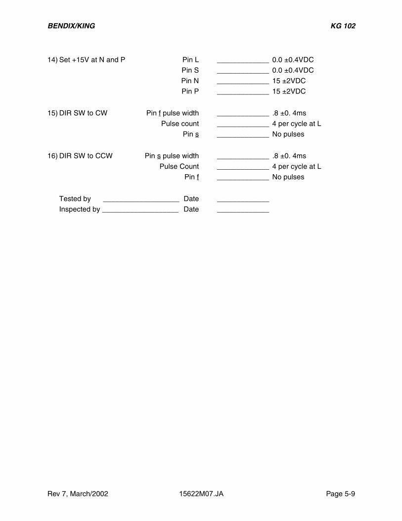
14) Set +15V at N and P Pin L _____________ 0.0 ±0.4VDC
Pin S _____________ 0.0 ±0.4VDC
Pin N _____________ 15 ±2VDC
Pin P _____________ 15 ±2VDC
15) DIR SW to CW Pin f pulse width _____________ .8 ±0. 4ms
Pulse count _____________ 4 per cycle at L
Pin s _____________ No pulses
16) DIR SW to CCW Pin s pulse width _____________ .8 ±0. 4ms
Pulse Count _____________ 4 per cycle at L
Pin f _____________ No pulses
Tested by ___________________ Date _____________
Inspected by ___________________ Date _____________

BENDIX/KING KG 102
Page 5-10 15622M07.JA Rev 7, March/2002
THIS PAGE IS RESERVED

BENDIX/KING KG 102
Rev 7, March/2002 15622M07.JA Page 5-11
GYRO TEST DATA SHEET
1) Unit 14V-28V to 14V. Gyro start voltage _____________ 0.38 ±0.10VAC
Gyro sim to SIM Run up _____________ 3 Min Max
14v/28v pwr to 14v Gyro run voltage _____________ 0.29 ±0.08VAC
Pin D _____________ +8.3 ±0.8VDC
_____________ or -6. 3 ±0.6VDC
Pin E _____________ +8.3 ±0.8 VDC
_____________ or -6.3 ±0.6VDC
2) Rotate Gyro for D and E
opposite to above Pin D _____________ -6.3 ±0.6VDC
_____________ or +8.3 ±0.8VDC
Pin E _____________ -6.3 ±0.6VDC
_____________ or +8.3 ± 0.8VDC
Gyro Connector
Pins A to B _____________ 26 ±3VAC
Pin C _____________ +5 ± 0.2VDC
Pin F _____________ +15 ±0.5VDC
Pin J _____________ -15 ± 0.5VDC
3) Turntable CCW Rise Time D _____________ 500us Max
1800 deg/min Fall Time D _____________ 500us Max
Rise Time E _____________ 500us Max
Fall Time E _____________ 500us Max
Card _____________ CCW
4) Push Gyro fail reset. _____________ No fail light
Rotate gyro 360 deg. at 1800 deg/min.
5) Stop table. North under CW Heading _____________ 0.0 ±2 deg
lubber line. Start table CW
at 1800 deg/min for 360 deg.
CCW Heading _____________ 0.2 ±2 deg

BENDIX/KING KG 102
Page 5-12 15622M07.JA Rev 7, March/2002
6) Five minutes on scorsby table. Card _____________ 0.0 ±2 deg
Level and put NORTH under
lubber line. Set table to
3 deg and adjust for 5 to 7
cycles per min. Run 10
min. Stop, level table.
7) NORTH under lubber line. Compass Card _____________ less than 1 deg motion.
CURRENT INTERRUPT for
less than one second.
Tested by ___________________ Date _____________
Inspected by ___________________ Date _____________
BENDIX/KING KG 102
Rev 7, March/2002 15622M07.JA Page 5-13
FINAL TEST DATA SHEET
1) Unit 14V-28V SW to 14V. Card _____________ No Motion
14V power on. Wait 2 min
Flux Valve input CW Pin Z to t _____________ 8.5 ±2VAC
Pin p to t _____________ 26 ±3VAC
_____________ 400 ±30Hz
Pin F to D _____________ 15 ±2VDC
Pin H to Y _____________ 15 ±0.5VDC
Pin K to Y _____________ -15 ±0. 5VDC
Pin T to V _____________ 5 ±0. 2VDC
Pin k _____________ 3.5 ± 0. 5VDC
2) Slave Switch ON Card _____________ Fast CCW
Wait 10 sec
Flux Valve CCW Card _____________ Fast CW
Wait 65 sec Card _____________ High Speed stops
Slave switch OFF _____________ Pulses 5 ± 1 sec
3) Slave SW CW Card _____________ CW fast
Slave SW CCW Card _____________ CCW fast
Slave Switch ON
Wait 65 sec
4) Flux Valve CW Card _____________ CCW slow
Slave SW OFF _____________ Pulses 5 ±1 sec
5) Unit on table for North under Card _____________ 0.0 ±2 deg
lubber line. Table CW 1800
deg/min for 360 deg. CCW
1800 deg/min for 360 deg. Card _____________ 0.0 ±2 deg
Tested by ___________________ Date _____________
Inspected by ___________________ Date _____________

BENDIX/KING KG 102
Page 5-14 15622M07.JA Rev 7, March/2002
THIS PAGE IS RESERVED

BENDIX/KING KG 102
Rev 7, March/2002 15622M07.JA Page 5-15
5.3 GENERAL OVERHAUL
5.3.1 VISUAL INSPECTION
This section contains instructions and information to assist in determining, by visual inspection, the condition of the units major assemblies and subassemblies. These inspection procedures will assist in finding defects resulting from wear, physical damage, deterioration, or other causes. To aid inspection, detailed procedures are arranged in alphabetical order.
A. Capacitors, FixedInspect capacitors for case damage, body damage, and cracked, broken, or charred insulation. Check for loose, broken, or corroded terminal studs, lugs, or leads. Inspect for loose, broken, or improperly soldered connections. On chip caps, be especially alert for hairline cracks in the body and broken terminations.
B. Capacitors, VariableInspect trimmers for chipped and cracked bodies, damaged dielectrics, and dam-aged contacts.
C. ChassisInspect the chassis for loose or missing mounting hardware, deformation, dents, damaged fasteners, or damaged connectors. In addition, check for corrosion or damage to the finish that should be repaired.
D. Circuit BoardsInspect for loose, broken, or corroded terminal connections; insufficient solder or improper bonding; fungus, mold, or other deposits; and damage such as cracks, burns, or charred traces.
E. ConnectorsInspect the connector bodies for broken parts; check the insulation for cracks, and check the contacts for damage, misalignment, corrosion, or bad plating. Check for broken, loose, or poorly soldered connections to terminals of the connectors. In-spect connector hoods and cable clamps for crimped wires.
F. Covers and ShieldsInspect covers and shields for punctures, deep dents, and badly worn surfaces. Al-so, check for damaged fastener devices, corrosion and damage to finish.
G. Flex CircuitsInspect flex circuits for punctures, and badly worn surfaces. Check for broken trac-es, especially near the solder contact points.
H. Front PanelCheck that name, serial, and any plates or stickers are secure and hardware is tight. Check that the handle is functional, securely fastened, and handle casting is not damaged or bent.
I. FuseInspect for blown fuse and check for loose solder joints.
J. InsulatorsInspect insulators for evidence of damage, such as broken or chipped edges, burned areas, and presence of foreign matter.
K. JacksInspect all jacks for corrosion, rust, deformations, loose or broken parts, cracked insulation, bad contacts, or other irregularities.

BENDIX/KING KG 102
Page 5-16 15622M07.JA Rev 7, March/2002
L. PotentiometersInspect all potentiometers for evidence of damage or loose terminals, cracked in-sulation or other irregularities.
M. Resistors, FixedInspect the fixed resistors for cracked, broken, blistered, or charred bodies and loose, broken, or improperly soldered connections. On chip resistors, be especially alert for hairline cracks in the body and broken terminations.
N. RF CoilsInspect all RF coils for broken leads, loose mountings, and loose, improperly sol-dered, or broken terminal connections. Check for crushed, scratched, cut or charred windings. Inspect the windings, leads, terminals and connections for cor-rosion or physical damage. Check for physical damage to forms and tuning slug adjustment screws.
O. Terminal Connections Soldered(1) Inspect for cold-soldered or resin joints. These joints present a po-
rous or dull, rough appearance. Check for strength of bond using the points of a tool.
(2) Examine the terminals for excess solder, protrusions from the joint, pieces adhering to adjacent insulation, and particles lodged be-tween joints, conductors, or other components.
(3) Inspect for insufficient solder and unsoldered strands of wire pro-truding from the conductor at the terminal. Check for insulation that is stripped back too far from the terminal.
(4) Inspect for corrosion at the terminal.P. Transformers
(1) Inspect for signs of excessive heating, physical damage to the case, cracked or broken insulation, and other abnormal conditions.
(2) Inspect for corroded, poorly soldered, or loose connecting leads or terminals.
Q. Wiring/Coaxial CableInspect wiring in chassis for breaks in insulation, conductor breaks, cut or broken lacing and improper dress in relation to adjacent wiring or chassis.
5.3.2 CLEANING
A. GeneralThis section contains information to aid in the cleaning of the component parts and subassemblies of the unit.
WARNING:GOGGLES ARE TO BE WORN WHEN USINGPRESSURIZED AIR TO BLOW DUST ANDDIRT FROM EQUIPMENT. ALL PERSONNELSHOULD BE WARNED AWAY FROM THE IM-MEDIATE AREA.

BENDIX/KING KG 102
Rev 7, March/2002 15622M07.JA Page 5-17
WARNING:OPERATIONS INVOLVING THE USE OF ACLEANING SOLVENT SHOULD BE PER-FORMED UNDER A VENTILATED HOOD.AVOID BREATHING SOLVENT VAPOR ANDFUMES; AVOID CONTINUOUS CONTACTWITH THE SOLVENT. WEAR A SUITABLEMASK, GOGGLES, GLOVES, AND AN APRONWHEN NECESSARY. CHANGE CLOTHINGUPON WHICH SOLVENTS HAVE BEENSPILLED.
WARNING:OBSERVE ALL FIRE PRECAUTIONS FORFLAMMABLE MATERIALS. USE FLAMMABLEMATERIALS IN A HOOD PROVIDED WITHSPARK-PROOF ELECTRICAL EQUIPMENTAND AN EXHAUST FAN WITH SPARKPROOFBLADES.
B. Recommended Cleaning AgentsTable 5-1 lists the recommended cleaning agents to be used during overhaul of the unit.
NOTE:EQUIVALENT SUBSTITUTES MAY BE USED FORLISTED CLEANING AGENTS.
TABLE 5-1 RECOMMENDED CLEANING AGENTS
TYPE USED TO CLEAN
Denatured Alcohol Various, exterior and interior
DuPont Vertrel SMT Various, interior
PolaClear Cleaner (Polaroid Corp.) or Texwipe TX129 (Texwipe Co.)
CRT display filter, LCD displays, and general purpose lens/glass cleaner.
KimWipes lint-free tissue(Kimberly Clark Corp.)
Various
Cloth, lint-free cotton Various
Brush, flat with fiber bristles Various
Brush, round with fiber bristles Various
Dishwashing liquid (mild) Nylon, Rubber Grommets

BENDIX/KING KG 102
Page 5-18 15622M07.JA Rev 7, March/2002
C. Recommended Cleaning Procedures
CAUTION:DO NOT ALLOW SOLVENT TO RUN INTOSLEEVES OR CONDUIT THAT COVERSWIRES CONNECTED TO INSERT TERMI-NALS.
1. Exterior(a) Wipe dust cover and front panel with a lint-free cloth dampened with
denatured alcohol.(b) For cleaning connectors, use the following procedure.
(1) Wipe dust and dirt from bodies, shells, and cable clamps using a lint-free cloth moistened with dena-tured alcohol.
(2) Wipe parts dry with a clean, dry lint-free cloth.(3) Remove dirt and lubricant from connector inserts, in-
sulation, and terminals using a small soft bristled brush moistened with denatured alcohol.
(4) Dry the inserts with an air jet.(c) Remove cover(s).(d) If necessary, open any blocked ventilation holes by first saturating
the debris clogging the apertures with denatured alcohol and then blowing the loosened material out with an air stream.
2. InteriorThe following solvents are no longer recommended for benchtop or rework cleaning of printed circuit boards, modules, or sub-assem-blies.
TABLE 5-2 UNSAFE CLEANING AGENTS
FREON TF, IMC TRICHLOROETHANE
CARBON TETRACHLORIDE DETERGENT (ALL AND EQUIVALENTS)
CHLOROFORM METHYLENE CHLORIDE
TRICHLOROETHYLENE GENESOLV 2004/2010
PROPYL ALCOHOL METHYL ALCOHOL
ETHYL ALCOHOL BUTYL ALCOHOL
XYLENE PRELETE (CFC-113)

BENDIX/KING KG 102
Rev 7, March/2002 15622M07.JA Page 5-19
CAUTION:DO NOT USE SOLVENT TO CLEAN PARTSCOMPOSED OF OR CONTAINING NYLON ORRUBBER GROMMETS. CLEAN THESEITEMS WITH MILD LIQUID DISHWASHINGDETERGENT AND WATER. USE DETER-GENT FOR THIS PURPOSE ONLY.
CAUTION:DUPONT VERTREL SMT DOES HAVE GEN-ERAL MATERIAL COMPATIBILITY PROB-LEMS WITH POLYCARBONATE, POLYSTY-RENE, AND RUBBER. IT IS RECOMMENDEDTHAT THESE MATERIALS BE CLEANEDWITH DENATURED ALCOHOL.
CAUTION:DO NOT ALLOW EXCESS CLEANING SOL-VENT TO ACCUMULATE IN ANY OF THE AD-JUSTMENT SCREW CREVICES AND THERE-BY SOFTEN OR DISSOLVE THE ADJUST-MENT SCREW EPOXY SEALANT.
CAUTION:AVOID AIR-BLASTING SMALL TUNING COILSAND OTHER DELICATE PARTS BY HOLDINGTHE AIR NOZZLE TOO CLOSE. USE BRUSH-ES CAREFULLY ON DELICATE PARTS.
CAUTION:IMPROPER CLEANING CAN RESULT IN SUR-FACE LEAKAGE AND CONDUCTIVE PARTIC-ULATES, SUCH AS SOLDER BALLS OR ME-TALLIC CHIPS, WHICH CAN CAUSE ELEC-TRICAL SHORTS. SEVERE IONIC CONTAM-INATION FROM HANDLING AND FROMENVIRONMENTAL CONDITIONS CAN RE-SULT IN HIGH RESISTANCE OR OPEN CIR-CUITS.
CAUTION:ULTRASONIC CLEANING CAN DAMAGECERTAIN PARTS AND SHOULD GENERALLYBE AVOIDED.

BENDIX/KING KG 102
Page 5-20 15622M07.JA Rev 7, March/2002
NOTE:Solvents may be physically applied in several waysincluding agitation, spraying, brushing, and vapordegreasing. The cleaning solvents and methodsused shall have no deleterious effect on the parts,connections, and materials being used. If sensitivecomponents are being used, spray is recommended.Uniformity of solvent spray flow should be maxi-mized and wait-time between soldering and cleaningshould be minimized.
NOTE:Clean each module subassembly. Then remove anyforeign matter from the casting.
Remove each module subassembly. Then remove any foreign mat-ter from the casting.(a) Casting covers and shields should be cleaned as follows:
(1) Remove surface grease with a lint-free cloth.(2) Blow dust from surfaces, holes, and recesses using
an air stream.(3) If necessary, use a solvent, and scrub until clean,
working over all surfaces and into all holes and re-cesses with a suitable non-metallic brush.
(4) Position the part to dry so the solvent is not trapped in holes or recesses. Use an air stream to blow out any trapped solvent.
(5) When thoroughly clean, touch up any minor damage to the finish.
(b) Assemblies containing resistors, capacitors, rf coils, inductors, transformers, and other wired parts should be cleaned as follows:
(1) Remove dust and dirt from all surfaces, including all parts and wiring, using soft-bristled brushes in con-junction with air stream.
(2) Any dirt that cannot be removed in this way should be removed with a brush (not synthetic) saturated with an approved solvent, such as mentioned above. Use of a clean, dry air stream (25 to 28 psi) is recom-mended to remove any excess solvent.
(3) Remove flux residue, metallic chips, and/or solder balls with an approved solvent.
(c) Wired chassic devices containing terminal boards, resistor and ca-pacitor assemblies, rf coils, switches, sockets, inductors, transform-ers, and other wired parts should be cleaned as follows:

BENDIX/KING KG 102
Rev 7, March/2002 15622M07.JA Page 5-21
NOTE:When necessary to disturb the dress of wires andcables, note the positions before disturbing and re-store them to proper dress after cleaning.
(1) Blow dust from surfaces, holes, and recesses using an air jet.
(2) Finish cleaning chassis by wiping finished surfaces with a lint-free cloth moistened with solvent.
(3) Dry with a clean, dry, lint-free cloth.(4) When thoroughly clean, touch-up any minor damage
to the finish.(5) Protect the chassis from dust, moisture, and damage
pending inspection.(d) Ceramic and plastic parts should be cleaned as follows:
(1) Blow dust from surfaces, holes, and recesses using an air jet.
(2) Finish cleaning chassis by wiping finished surfaces with a lint-free cloth moistened with solvents.
(3) Dry with a clean, dry, lint-free cloth.
5.3.3 REPAIR
A. GeneralThis section contains information required to perform limited repairs on the unit. The repair or replacement of damaged parts in airborne electronic equipment usu-ally involves standard service techniques. In most cases, examination of drawings and equipment reveals several approaches to perform a repair. However, certain repairs demand following an exact repair sequence to ensure proper operation of the equipment. After correcting a malfunction in any section of the unit, it is recom-mended that a repetition of the functional test of the unit be performed.
B. Repair Precautions1. Ensure that all ESDS and MOS handling precautions are followed.2. Perform repairs and replace components with power disconnected
from equipment.3. Use a conductive table top for repairs and connect table to ground
conductors of 60Hz and 400Hz power lines.4. Replace connectors, coaxial cables, shield conductors, and twisted
pairs only with identical items.5. Reference “component side” of a printed circuit board in this manual
means the side on which components are located; “solder side” re-fers to the other side. The standard references are as follows: near-side is the component side; farside is the solder side; on surface mount boards with components on both sides, the nearside is the side that has the J#### and P#### connector numbers.
6. When repairing circuits, carefully observe lead dress and compo-nent orientation. Keep leads as short as possible and observe cor-rect repair techniques.

BENDIX/KING KG 102
Page 5-22 15622M07.JA Rev 7, March/2002
7. There are certain soldering considerations with surface mount com-ponents. The soldering iron tip should not touch the ceramic com-ponent body. The iron should be applied only to the termination-sol-der filet.
8. Observe cable routing throughout instrument assembly, prior to dis-assembly, to enable a proper reinstallation of cabling during reas-sembly procedures.
CAUTIONTHIS EQUIPMENT CONTAINS ELECTRO-STATIC DISCHARGE SENSITIVE (ESDS) DE-VICES. EQUIPMENT MODULES AND ESDSDEVICES MUST BE HANDLED IN ACCOR-DANCE WITH SPECIAL ESDS HANDLINGPROCEDURES.
C. Electrostatic Sensitive Devices (ESDS) Protection1. Always discharge static before handling devices by touching some-
thing that is grounded.2. Use a wrist strap grounded through a 1MΩ resistor.3. Do not slide anything on the bench. Pick it up and set it down in-
stead.4. Keep all parts in protective cartons until ready to insert into the
board.5. Never touch the device leads or the circuit paths during assembly.6. Use a grounded tip, low wattage soldering station.7. Keep the humidity in the work environment as high as feasibly pos-
sible.8. Use grounded mats on the work station unless table tops are made
of approved antistatic material.9. Do not use synthetic carpet on the floor of the shop. If a shop is car-
peted, ensure that a grounded mat is placed at each workstation.10. Keep common plastics out of the work area.
D. MOS Device ProtectionMOS (Metal Oxide Semiconductor) devices are used in this equipment. While the attributes of MOS type devices are many, characteristics make them susceptible to damage by electrostatic or high voltage charges. Therefore, special precautions must be taken during repair procedures to prevent damaging the device. The fol-lowing precautions are recommended for MOS circuits, and are especially impor-tant in low humidity or dry conditions.1. Store and transport all MOS devices in conductive material so that
all exposed leads are shorted together. Do not insert MOS devices into conventional plastic “snow” or plastic trays used for storing and transporting standard semiconductor devices.

BENDIX/KING KG 102
Rev 7, March/2002 15622M07.JA Page 5-23
2. Ground working surfaces on workbench to protect the MOS devic-es.
3. Wear cotton gloves or a conductive wrist strap in series with a 200KΩ resistor connected to ground.
4. Do not wear nylon clothing while handling MOS devices.5. Do not insert or remove MOS devices with power applied. Check all
power supplies to be used for testing MOS devices. and be sure that there are no voltage transients present.
6. When straightening MOS leads, provide ground straps for the appa-ratus for the device.
7. Ground the soldering iron when soldering a device.8. When possible, handle all MOS devices by package or case, and
not by leads. Prior to touching the device, touch an electrical ground to displace any accumulated static charge. The package and substrate may be electrically common. If so, an electrical dis-charge to the case would cause the same damage as touching the leads.
9. Clamping or holding fixtures used during repair should be ground-ed, as should the circuit board, during repair.
10. Devices should be inserted into the printed circuit boards such that leads on the back side do not contact any material other than the printed circuit board (in particular, do not use any plastic foam as a backing).
11. Devices should be soldered as soon as possible after assembly. All soldering irons must be grounded.
12. Boards should not be handled in the area around devices, but rather by board edges.
13. Assembled boards must not be placed in conventional, home-type, plastic bags. Paper bags or antistatic bags should be used.
14. Before removing devices from conductive portion of the device car-rier, make certain conductive portion of carrier is brought in contact with well grounded table top.
E. PC Board, Two-Lead Component Removal (Resistors, Capacitors, Diodes, etc.)1. Heat one lead from component side of board until solder flows, and
lift one lead from board; repeat for other lead and remove compo-nent (note orientation).
2. Melt solder in each hole, and using a desoldering tool, remove sol-der from each hole.
3. Dress and form leads of replacement component; insert leads into correct holes.
4. Insert replacement component observing correct orientation.
F. PC Board, Multi-Lead Component Removal (IC’s, etc.)1. Remove component by clipping each lead along both sides. Clip off
leads as close to component as possible. Discard component.2. Heat hole from solder side and remove clipped lead from each hole.

BENDIX/KING KG 102
Page 5-24 15622M07.JA Rev 7, March/2002
3. Melt solder in each hole, and using a desoldering tool, remove sol-der from each hole.
4. Insert replacement component observing correct orientation.5. Solder component in place from farside of board. Avoid solder runs.
No solder is required on contacts where no traces exist.
G. Replacement of Power Transistors1. Unsolder leads and remove attaching hardware. Remove transistor
and hard-coat insulator.2. Apply Thermal Joint Compound Type 120 (Wakefield Engineering,
Inc.) to the mounting surface of the replacement transistor.3. Reinstall the transistor insulator and the power transistor using
hardware removed in step (1).4. After installing the replacement transistor, but before making any
electrical connections, measure the resistance between the case of the transistor and the chassis, to ensure that the insulation is effec-tive. The resistance measured should be greater than 10MΩ.
5. Reconnect leads to transistor and solder in place.
H. Replacement of Printed Circuit Board Protective Coating
WARNINGCONFORMAL COATING CONTAINS TOXICVAPORS! USE ONLY WITH ADEQUATE VEN-TILATION.
1. Clean repaired area of printed circuit board per instructions in the Cleaning section of this manual.
2. Apply Conformal Coating, Humiseal #1B-31 HYSOL PC20-35M-01 (Humiseal Division, Columbia Chase Corp., 24-60 Brooklyn Queens Expressway West, Woodside, N.Y., 11377) P/N 016-01040-0000.
3. Shake container well before using.4. Spray or brush surfaces with smooth, even strikes. If spraying, hold
nozzle 10-15 inches from work surface.5. Cure time is ten minutes at room temperature.
I. Programmable Read Only Memory (PROM) ReplacementThe read only memory packages are specially programmed devices to provide specific logic outputs required for operation in the unit. The manufacturer’s part (type) number is for the un-programmed device, and cannot be used. The Honey-well part number must be used to obtain the correctly programmed device. Refer to the “Illustrated Parts List” (IPL).

BENDIX/KING KG 102
Rev 7, March/2002 15622M07.JA Page 5-25
5.3.3.1 REPLACEMENT OF COMPONENTS
This section describes the procedure, along with any special techniques, for replacing damaged or defective components.
A. ConnectorsWhen replacing a connector, refer to the appropriate PC board assembly drawing, and follow the notes, to ensure correct mounting and mating of each connector.
B. CrystalThe use of any crystal, other than a Honeywell crystal, is considered an unautho-rized modification.
C. DiodesDiodes used are silicon and germanium. Use long-nose pliers as a heat sink, under normal soldering conditions. Note the diode polarity before removal.
D. Integrated CircuitsRefer to the applicable reference for removal and replacement instructions.
E. Wiring/Coaxial CableWhen repairing a wire that has broken from its terminal, remove all old solder, and pieces of wire from the terminal, re-strip the wire to the necessary length, and resol-der the wire to the terminal. Replace a damaged wire or coaxial cable with one of the same type, size and length.
5.4 DISASSEMBLY/ASSEMBLY PROCEDURESThe following instructions included the procedures that are necessary to remove and disassemble the subassemblies of the KG 102.It is assumed that the unit has been tested in accordance with the test procedures provided in paragraph 5.2 to locate the source of the malfunction. The unit should be disassembled only to the station where the malfunction can be corrected by repair, cleaning, or adjustment. Do not dis-assemble any parts or wiring unnecessarily as repeated tear downs can be detrimental to the life of the unit.The KG 102 is comprised of three major subassemblies and a final assembly. The final assembly contains the necessary hardware and components required to bring the subassemblies together into a functional unit. This Section 5.4 covers disassembly of two of the three subassemblies. The third subassembly, the directional gyro, is covered in detail in Section 5.5.3.Disassembly instructions are provided to separate the subassemblies from the basic unit, howev-er, detailed breakdown of the components on each subassembly has not been included as this can be accomplished by referring to the subassembly drawings (Section VI). Reassembly can be accomplished by reversing the disassembly procedures.
WARNINGREMOVE ALL POWER FROM THE UNIT BE-FORE DISASSEMBLY OF ANY MODULE. BE-SIDES BEING DANGEROUS TO LIFE, VOLT-AGE TRANSIENTS CAN CAUSE CONSIDER-ABLE DAMAGE TO THE EQUIPMENT.

BENDIX/KING KG 102
Page 5-26 15622M07.JA Rev 7, March/2002
CAUTIONEXERCISE EXTREME CARE WHEN DISCON-NECTING AND RECONNECTING MULTIPLEPIN CONNECTORS, TO ENSURE THAT THECONNECTORS ARE NOT DAMAGED BY MIS-ALIGNMENT OF THE PINS.
CAUTIONTHIS EQUIPMENT CONTAINS ELECTRO-STATIC DISCHARGE SENSITIVE (ESDS) DE-VICES. EQUIPMENT, MODULES, AND ESDSDEVICES MUST BE HANDLED IN ACCOR-DANCE WITH SPECIAL ESDS HANDLINGPROCEDURES.
5.4.1 ELECTRONICS ASSEMBLY REMOVAL
A. Remove four screws and then remove the bottom cover.B. Remove the three screws holding the gyro subassembly, slide the gyro subassem-
bly away from the unit and disconnect the 9-pin connector.C. Remove the two screws (089-05907-0006) in the center of the top of the unit and
remove the electronics subassembly.D. When in this state of disassembly, the components of both the power supply P. C.
board subassembly and the logic P. C. board subassembly are readily accessible.
5.5 GYRO OVERHAUL (P/N 060-0011-00)
5.5.1 INSPECTION
In general, all parts should be examined for defects and discrepancies which would impair the function of the part.
A. Examine machined surfaces, diameters, shoulders and threads which mate with another part for nicks, burns, flashing, the unnecessary residue of epoxy or adhe-sive, scratches and excessive wear.
B. Minor scratches and nicks noted, as in preceding step, may be smoothed with India stone, crocus cloth, or red rouge.
C. Slip rings must be examined critically under strong light and with magnification. Look for scratches, burn pits, epoxy splatters, discoloration, etc. Removal of slight scratches and discoloration are possible by lighting polishing with red rouge mixed in light oil. A piece of pith wood makes a convenient polishing tool. Slip rings must have a bright, smooth continuous finish around 360 degrees of each ring. (Pitted rings should be rejected because they will probably soon fail in the brush contact area and will cause excessive friction and additional burning). Thoroughly clean slip rings after polishing.
D. Ball bearings are difficult to evaluate and mechanically inspect without rather com-plicated electronic and mechanical fixturing. Consequently, much depends upon the judgement and experience of overhaul personnel with regard to the acceptance or rejection of a used bearing.

BENDIX/KING KG 102
Rev 7, March/2002 15622M07.JA Page 5-27
Experience gained in the testing of the gyro will tell much about bearing perfor-mance. Ball bearings, when axially loaded to nominal values, should feel "smooth" when rotated. There should be no detectable snagging of balls in the races, and no ball and retainer wrap-up which is indicated by momentary increases in the friction. Roughness, snagging and wrap-up as well as inner-outer race misalignment are all detrimental in gimbal operation because of the very small rotational rates that are typical of gimbal movement.
E. Spin axis bearing faults are more evident during operation because of the high ro-tational velocity. A gyro motor assembly may be bench mounted and spin perfor-mance observed, felt and heard as power is applied or during run-down. Preload conditions can be felt with power off by holding motor shaft between thumb and forefinger while rotating or spinning the rotor.
F. Encoder disc should be bonded firmly for full 360 degrees of contact with the spac-er beneath it. The Fiberglas spacer, must, in turn, be firmly bonded for 360 degrees to the outer gimbal shoulder. Any separation between outer gimbal and Fiberglas spacer may be repaired with application of Hysol (part number 005-02002-0061) providing that perpendicularity of the encoder disc to the outer gimbal axis is held within 0.003 inch total indicator reading. Use a pointed applicator to apply Hysol to the fissure where parts have separated. Cure the adhesive at room ambient tem-perature and humidity.
G. If encoder disc perpendicularity limit (0.003 inch TIR) is exceeded, no attempt should be made to reseat the disc to meet the requirement. Replace entire gimbal assembly (25) if perpendicularity is out of limit.
H. Carefully examine, with optical magnification, the reticle pattern on the encoder disc. Theoretically the LED light falls midway, radially speaking, in the reticle pat-tern. Allowing for radial stack-up of all tolerances involved, discrepancies in the window pattern can not be tolerated except at extreme inner and outer ends of the windows. Scratches and/or transparencies in the black opaqued section, and irreg-ularity of the edges of the windows will produce erroneous signals if they appear in the critical pattern band. Transparent (or even translucent) spots in the opaque web will cause a random spurious signal which would be unacceptable. A random opaque material in a window area will disrupt the trigger increment (as, for exam-ple, a small spatter of solder) such that it will not occur at the precise edge of a win-dow.
I. Rotate gimbal disc assembly and observe the inner or outer ends of the windows for runout. Runout shall not exceed 0. 002 inch total indicator reading.
J. Examine circuit board assembly for signs of burned (overheated) components and poor solder joints.
5.5.2 GYRO CLEANING
5.5.2.1 Cleaning of Parts
Parts cleaning procedures given in the manual are primarily applicable to repair and reassembly at overhaul facilities. New parts from supply sources should be handled with same procedures as used parts to ensure that parts are properly cleaned, have all protective coatings removed, and are ready for installation.

BENDIX/KING KG 102
Page 5-28 15622M07.JA Rev 7, March/2002
5.5.2.2 SPECIAL TOOLS FOR CLEANING AND INSPECTION.
Refer to the approved cleaners in section 5.3.2.B. The following list comprises material and de-vices useful in the cleaning and inspection of parts of the gyro not listed in 5.3.2.B.
1) Approved cleaning material are as follows:
a Red Rouge, Polishing (very fine grit)
b. Machine Oil (low viscosity)
2) Equipment and tools are as follows:
a. Artist’s Brushes (assorted sizes) or equivalent.
b. Clean Cotton Swabs
c. Vacuum Source
d. Compressed Air Source (filtered)
e. Dental Picks and Chisels, or equivalent
f. Electric Oven
g. India Stones, or Polishing Paper (Rouge)
h. Pipe Cleaners
i. Eye Loupe, or Microscope
5.5.2.3 CLEANING
All individual fabricated metal parts except ball bearings, may be cleaned by submersion, by brushing or by spraying with DuPont Vertrel SMT. Remove excess solvent after cleaning by blow-ing with clean, dry compressed air or vacuum dry the parts. Other parts require specific handling as follows:
1) Assemblies which can not be submerged in a solvent because of adhesive joint or ball bearings can generally be brush cleaned with DuPont Vertrel SMT. Rapid dry with compressed air or with vacuum.
2) Molded plastic parts may be cleaned with DuPont Vertrel SMT. Rapid drying is re-quired following cleaning.
3) Gold plated brushes and slip rings should be gently cleaned by applying DuPont Vertrel SMT with an artist’s brush or a cotton swab. Rapid removal of excess solvent is necessary to prevent possible attack on adjacent molded components.
4) Switch assemblies usually require only dry brushing with a vacuum source. If nec-essary, brush application of DuPont Vertrel SMT followed by rapid drying may be used.
5) Circuit board assembly may be cleaned by brushing with DuPont Vertrel SMT. Rapid drying should follow cleaning.
6) Denatured alcohol may be used to clean soldering flux from around terminals, but care must be exercised that the alcohol does not remove artwork on circuit board.
7) Bearing retainer and bearing bores must have all old epoxy removed. Clean with Du-Pont Vertrel SMT.
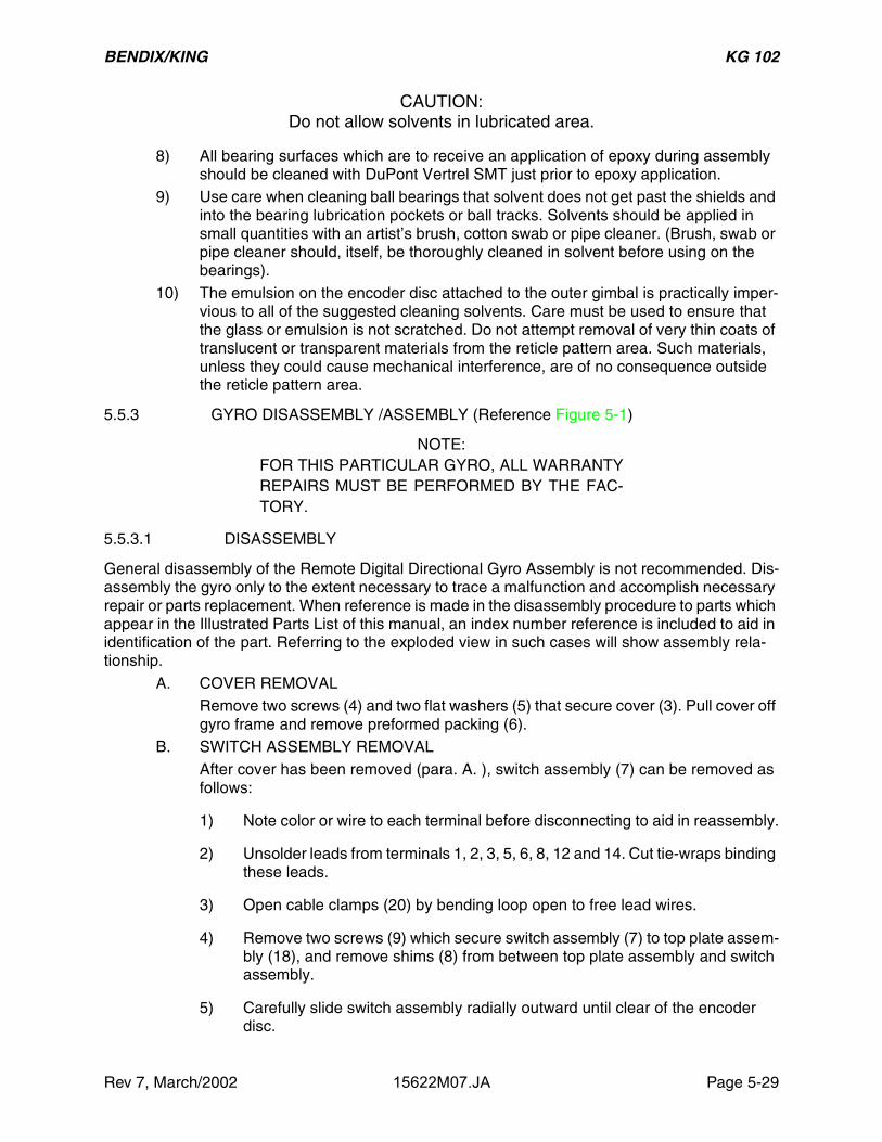
BENDIX/KING KG 102
Rev 7, March/2002 15622M07.JA Page 5-29
CAUTION:Do not allow solvents in lubricated area.
8) All bearing surfaces which are to receive an application of epoxy during assembly should be cleaned with DuPont Vertrel SMT just prior to epoxy application.
9) Use care when cleaning ball bearings that solvent does not get past the shields and into the bearing lubrication pockets or ball tracks. Solvents should be applied in small quantities with an artist’s brush, cotton swab or pipe cleaner. (Brush, swab or pipe cleaner should, itself, be thoroughly cleaned in solvent before using on the bearings).
10) The emulsion on the encoder disc attached to the outer gimbal is practically imper-vious to all of the suggested cleaning solvents. Care must be used to ensure that the glass or emulsion is not scratched. Do not attempt removal of very thin coats of translucent or transparent materials from the reticle pattern area. Such materials, unless they could cause mechanical interference, are of no consequence outside the reticle pattern area.
5.5.3 GYRO DISASSEMBLY /ASSEMBLY (Reference Figure 5-1)
NOTE:FOR THIS PARTICULAR GYRO, ALL WARRANTYREPAIRS MUST BE PERFORMED BY THE FAC-TORY.
5.5.3.1 DISASSEMBLY
General disassembly of the Remote Digital Directional Gyro Assembly is not recommended. Dis-assembly the gyro only to the extent necessary to trace a malfunction and accomplish necessary repair or parts replacement. When reference is made in the disassembly procedure to parts which appear in the Illustrated Parts List of this manual, an index number reference is included to aid in identification of the part. Referring to the exploded view in such cases will show assembly rela-tionship.
A. COVER REMOVALRemove two screws (4) and two flat washers (5) that secure cover (3). Pull cover off gyro frame and remove preformed packing (6).
B. SWITCH ASSEMBLY REMOVALAfter cover has been removed (para. A. ), switch assembly (7) can be removed as follows:
1) Note color or wire to each terminal before disconnecting to aid in reassembly.
2) Unsolder leads from terminals 1, 2, 3, 5, 6, 8, 12 and 14. Cut tie-wraps binding these leads.
3) Open cable clamps (20) by bending loop open to free lead wires.
4) Remove two screws (9) which secure switch assembly (7) to top plate assem-bly (18), and remove shims (8) from between top plate assembly and switch assembly.
5) Carefully slide switch assembly radially outward until clear of the encoder disc.

BENDIX/KING KG 102
Page 5-30 15622M07.JA Rev 7, March/2002
C. CIRCUIT BOARD REMOVAL.After cover has been removed (para. A), circuit board assembly (10, figure 5-1) can be removed as follows:
1) Note color of wire to each terminal before disconnecting to aid is reassembly.
2) Unsolder leads from terminals on circuit board assembly.
3) Remove two screws (12) and one screw (11). Lift off circuit board assembly (10) and three stops (13) from under the board in line with attaching screw holes.
D. MOTOR REMOVALAfter the cover has been removed (para. A.) the gyro motor (39) may be removed with gimbal assembly (25) remaining in the frame (24) as follows, or the gyro motor removal may be accomplished after the rotor housing assembly (46) and rotor hous-ing cap (37) have been removed from the outer gimbal and encoder disc assembly as noted in step G.
1) Note wire colors at the three terminals in rotor housing cap (37, figure 5-1) be-fore disconnecting to aid in reassembly.
2) Unsolder leads from the three terminals. Separate and dress leads straight, then withdraw from rotor housing cap along with insulation sleeving. Leads must remain attached to slip rings at one end of the inner gimbal axis.
3) Remove four screws (38) that attach rotor housing cap (37) to the rotor hous-ing assembly.
4) Remove any socket head setscrews (34) from bosses on rotor housing as-sembly that have threaded holes parallel to motor spin axis.
5) Move inner and outer gimbal as necessary to bring impeller end of the motor into position accessible through largest opening in the frame.
6) Attach special pulling tool to the rotor housing assembly, utilizing the tapped holes parallel to spin axis through the bosses on the housing, aligning driver on the tool with center of the motor shaft.
7) Carefully tighten driver of the tool to gradually increase pressure on the motor shaft until epoxy seal is broken and motor end cap is pressed out of the hous-ing.
8) Remove rotor housing cap (37) and motor assembly (39) from rotor housing assembly (46). Remove any spacers (40) from the motor shaft at impeller end.
9) Clamp exposed end of motor shaft in a smooth bore Colette to hold motor while removing rotor housing cap (37) from the motor shaft.

BENDIX/KING KG 102
Rev 7, March/2002 15622M07.JA Page 5-31
E. GIMBAL ASSEMBLY REMOVALAfter the cover has been removed (step A.) and the switch assembly (step B.), the gimbal assembly (25) may be removed without first removing the circuit board as-sembly (step C.) if the electrical leads are loosened enough to provide adequate slack. Electrical contact brush (15) need not be removed from top plate assembly (18), but care must be exercised as noted when electrical contact brush is removed from the top plate or when the top plate, with brush is removed from the top plate or when the top plate, with brush attached, is removed.
1) Install a smooth cylindrical tube between slip rings and brush block, which is just large enough to hold brush wipers lifted off the slip rings during disassem-bly.
2) Remove two screws (19) and screw (11) securing top plate assembly (18).
3) Grasp inner gimbal between thumb and forefinger at motor shaft ends, and hold pressure on outer gimbal to keep it firmly seated in bearing at the end of the frame (24) while carefully lifting top plate assembly (18) from the frame.
4) Carefully lay the top plate assembly over against the outside of the frame, pro-tecting brushes, while still holding the inner gimbal.
5) With free hand, hold frame firmly and lift gimbal assembly (25) from the frame being extremely careful that the encoder disc does not strike on frame. Re-move ball bearing (21) from gimbal assembly if it retracted with the gimbal as-sembly. If the ball bearing remained in the frame, do not remove unless the bearing is suspect.

BENDIX/KING KG 102
Page 5-32 15622M07.JA Rev 7, March/2002
FIGURE 5-1 ELECTRICAL DIRECTIONAL GYRO ASSEMBLY EXPLODED VIEW(Sheet 1 of 2)

BENDIX/KING KG 102
Rev 7, March/2002 15622M07.JA Page 5-33
FIGURE 5-1 ELECTRICAL DIRECTIONAL GYRO ASSEMBLY EXPLODED VIEW(Sheet 2 of 2)
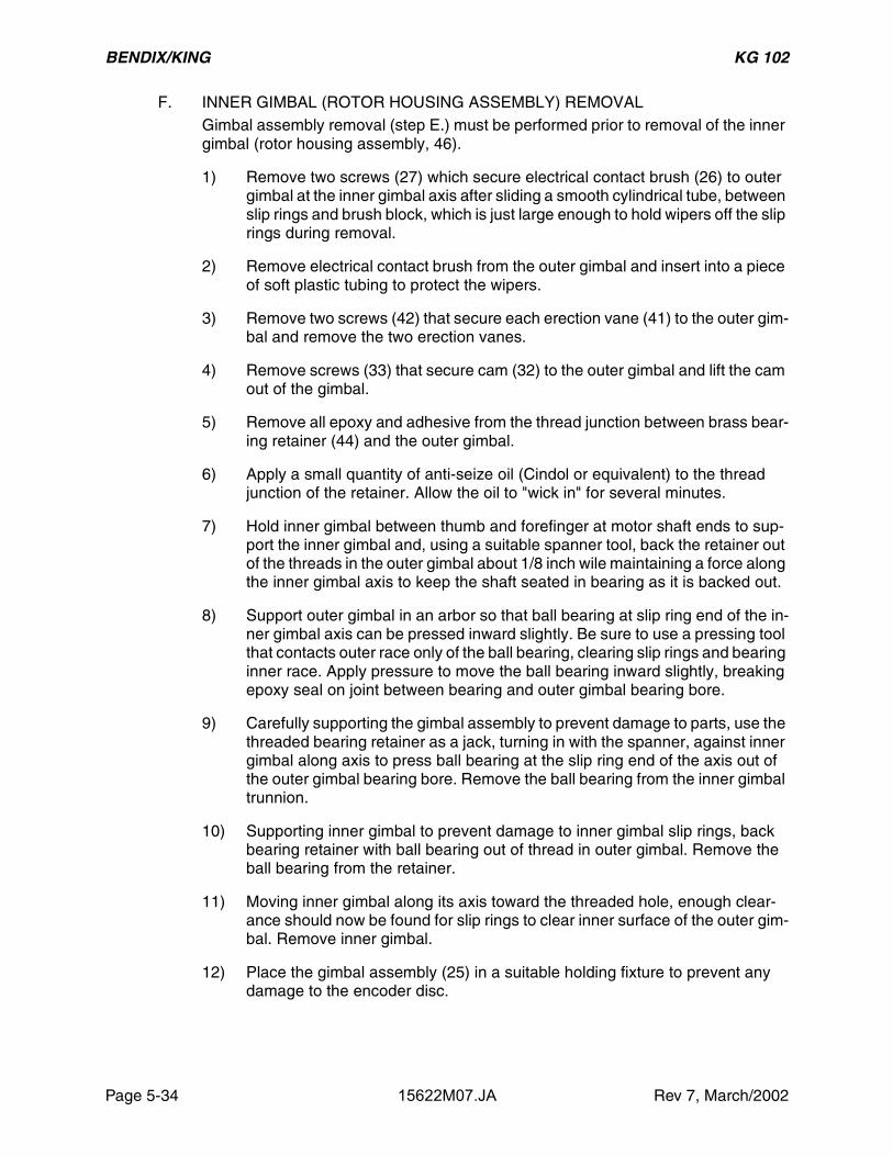
BENDIX/KING KG 102
Page 5-34 15622M07.JA Rev 7, March/2002
F. INNER GIMBAL (ROTOR HOUSING ASSEMBLY) REMOVALGimbal assembly removal (step E.) must be performed prior to removal of the inner gimbal (rotor housing assembly, 46).
1) Remove two screws (27) which secure electrical contact brush (26) to outer gimbal at the inner gimbal axis after sliding a smooth cylindrical tube, between slip rings and brush block, which is just large enough to hold wipers off the slip rings during removal.
2) Remove electrical contact brush from the outer gimbal and insert into a piece of soft plastic tubing to protect the wipers.
3) Remove two screws (42) that secure each erection vane (41) to the outer gim-bal and remove the two erection vanes.
4) Remove screws (33) that secure cam (32) to the outer gimbal and lift the cam out of the gimbal.
5) Remove all epoxy and adhesive from the thread junction between brass bear-ing retainer (44) and the outer gimbal.
6) Apply a small quantity of anti-seize oil (Cindol or equivalent) to the thread junction of the retainer. Allow the oil to "wick in" for several minutes.
7) Hold inner gimbal between thumb and forefinger at motor shaft ends to sup-port the inner gimbal and, using a suitable spanner tool, back the retainer out of the threads in the outer gimbal about 1/8 inch wile maintaining a force along the inner gimbal axis to keep the shaft seated in bearing as it is backed out.
8) Support outer gimbal in an arbor so that ball bearing at slip ring end of the in-ner gimbal axis can be pressed inward slightly. Be sure to use a pressing tool that contacts outer race only of the ball bearing, clearing slip rings and bearing inner race. Apply pressure to move the ball bearing inward slightly, breaking epoxy seal on joint between bearing and outer gimbal bearing bore.
9) Carefully supporting the gimbal assembly to prevent damage to parts, use the threaded bearing retainer as a jack, turning in with the spanner, against inner gimbal along axis to press ball bearing at the slip ring end of the axis out of the outer gimbal bearing bore. Remove the ball bearing from the inner gimbal trunnion.
10) Supporting inner gimbal to prevent damage to inner gimbal slip rings, back bearing retainer with ball bearing out of thread in outer gimbal. Remove the ball bearing from the retainer.
11) Moving inner gimbal along its axis toward the threaded hole, enough clear-ance should now be found for slip rings to clear inner surface of the outer gim-bal. Remove inner gimbal.
12) Place the gimbal assembly (25) in a suitable holding fixture to prevent any damage to the encoder disc.

BENDIX/KING KG 102
Rev 7, March/2002 15622M07.JA Page 5-35
G. GYRO MOTOR REMOVALThe gyro motor can be removed from the inner gimbal more rapidly when the inner gimbal has been removed in accordance with preceding step F.
1) Note wire colors to the three terminal studs to aid reassembly, then unsolder leads from the terminal studs. Separate and dress leads straight, and with-draw leads with sleeving from the motor end cap.
2) Remove four screws (38) from motor end cap (37).
3) Remove two balance trim screws (34) from threaded holes parallel to the mo-tor spin axis and install special pulling tool into the trim screw holes. Align driv-er on the pulling tool to center on motor shaft.
4) Apply pressure to motor shaft with the driver of the special pulling tool to break epoxy seal of end cover. Push motor shaft to the point where end cover and motor can be removed together. Remove spacers from motor shaft at the im-peller end.
5) Clamp accessible end of motor shaft in a smooth bore Colette and carefully twist end cover off other end of the motor.
H. CONNECTOR ASSEMBLY REMOVALIf necessary to remove the connector assembly for repair or parts replacement, the gimbal assembly must be removed first (step E).
1) Note color of leads which run to the three terminals (E6, E7, and E8) on the top plate assembly to aid in reassembly, and unsolder the leads. If necessary, remove phase shift capacitor from terminals (E6 and E7).
2) Unsolder leads from the circuit board assembly (unless circuit board was pre-viously removed) terminals 4, 7, 9, 10, 11 and 13.
3) Unwrap and dress out all loose leads.
4) Note colors of leads and unsolder leads from the electrical contact brush (15) unless the brush has been previously removed.
5) Ensuring that a bundle of leads with only wires that go to the connector is now prepared, grasp the bundle firmly and pull at an angle such that the leads and the tube (22) holding them to the channel in the frame are peeled out of the frame.
NOTE:Leave epoxy that remains on frame. It Will serve asa channel for remounting the tube.
6) Using a suitable spanner wrench, remove bushing from inside the frame (24) at back of the connector (23).
7) Remove epoxy from around the connector with suitable hand tools (a small soldering iron with chisel tip is helpful).
8) Carefully twist to loosen, and then press out the connector pulling attached wires with it.
BENDIX/KING KG 102
Page 5-36 15622M07.JA Rev 7, March/2002
5.5.3.2 ASSEMBLY AND ADJUSTMENT
Information in this section is presented in a sequence which can be used from complete disas-sembly. Calibration or adjustment applicable to the assembly procedure are presented in se-quence where such operations should be performed. Paragraph heads are provided as an aid to assembly from various levels of disassembly, as may be the situation when disassembly is per-formed only as necessary for repair or replacement. A prerequisite for assembly of any part or sub-assembly is that such parts will have been properly, cleaned and inspected in accordance with the applicable instructions of this manual. Reference to various adhesive compounds used in assem-bly is by specification control part number. A cross reference list appears in Section 5.5.3.3 which identifies the compounds to which each part number applies.
A. INSTALLATION OF CONNECTOR AND CABLE ASSEMBLYPrepare connector and cable assembly for installation and install in frame as fol-lows:
1) Check individual leads of the cable assembly for proper connection to connec-tor pins.
Yellow to Pin A Blue to pin D Black to pin HGreen to pin B Red to pin E Brown to pin JWhite to pin C Orange to pin F
2) Model RCA16A-6 only has a violet wire connected to pin K. Pin K is unused in Model RCA16A-5.
3) Remove mounting nut from back of connector (if installed) and thread loose ends of the leads through the connector mounting hole in the frame.
4) Apply adhesive, part number 005-02002-0003 (refer to Section 5.5.3.3 to out-side diameter of connector body and immediately install into the frame with pin D toward the gyro mounting face of the frame and anti-rotation tab en-gaged in lock hole provided.
5) Apply additional adhesive 005-02002-0003 around connector shell at inside junction with frame as necessary to complete the seal, then slide the mounting nut over the cable and thread onto the connector shell, tightening until bedded in the adhesive, and secure. Make sure anti-rotation tab stays in lock hole.
6) Dress leads along bottom of frame and position tube (22) on leads into the channel formed by original application of epoxy. Allow tube to extend out of the frame about 1/8 inch.
7) Hold tube close to frame by propping across inside of frame. Bridge tube with adhesive, part number 005-02002-0004, at several places to secure it to frame. Position frame on its side with tube down and cure adhesive for two hours at 140 deg. F.
8) Perform an insulation check by applying 500 volts dc with a megger between all connector pins in common and the frame for five seconds. Resistance must be at least 20 megohms.
B. INSTALLATION OF GYRO MOTORPrepare gyro motor (39) for installation and install in inner gimbal as follows:

BENDIX/KING KG 102
Rev 7, March/2002 15622M07.JA Page 5-37
1) Obtain three spacers (40), with a thickness totaling 0. 018 to 0. 020 inch, and install on motor shaft at impeller end.
2) Lightly "butter" the shaft bore in the rotor housing assembly (46) with adhe-sive, part number 005-02002-0004, so that shaft will be locked into the bore but not so much that adhesive is forced into motor bearing.
3) Install the motor assembly, impeller end first, into the rotor housing assembly so that motor shaft is entered into the prepared bore. Twist motor shaft as necessary to ensure that it is seated in the bore. Position the rotor housing as-sembly with open end up to keep the motor seated.
4) "Butter" shaft bore in rotor housing cap (37) with adhesive, part number 005-02002-0004, so that motor shaft will be locked in place but not so much that adhesive will be forced into motor bearing.
5) Keeping motor leads dressed into the groove in the motor shaft and free of adhesive, install rotor housing cap over the motor shaft into place at end of the rotor housing assembly. Cap must have cable retaining boss in line with cable boss in the housing assembly and screw holes aligned with tapped holes in the housing assembly. Secure the cap in place with four screws (38).
6) Hold motor with shaft vertical and rotor housing cap up so that weight of motor is maintained against the spacers installed in step 1. Insert a clean plastic rod through openings at the impeller end of the housing assembly and gently spin the rotor, observing coast down to verify that rotor is free of any bind.
CAUTION:If spin operation jars motor shaft upward awayfrom the spacers, press opposite end of theshaft to restore bottomed condition.
7) Mount motor and housing assembly in a suitable rack to maintain position of previous step while curing adhesive at 140’F for at least one hour.
8) Install inner gimbal slip ring leads with insulation sleeving through the lead re-taining boss in the rotor housing cap. Dress leads along motor housing. The insulation sleeving must be restrained in lead holes at each end with bonding compound, part number 005-02002-0002.
9) Ensure that motor leads are straight, then knot the leads twice close to the end of the motor shaft. Cut and strip motor leads to reach the three terminal studs in the end cap. With inner gimbal held so that terminals are toward view-er with the slip rings on right side, terminals are designated El, E2, and E3 reading from left to right. Solder slip ring leads and motor leads to the termi-nals with a light soldering iron and 60/40 solder routing yellow leads to El, green leads to E2 and motor violet lead to E3 with slip ring orange lead.
10) Dress all leads in close to the.end cap and clean soldered joints with alcohol .
11) Recheck rotational freedom of the gyro motor rotor as in preceding step 6) af-ter the wiring process of preceding step 9).

BENDIX/KING KG 102
Page 5-38 15622M07.JA Rev 7, March/2002
C. INSTALLATION OF INNER GIMBALPrepare inner gimbal for installation and install in the outer gimbal assembly as fol-lows. If gyro motor was removed from the inner gimbal, it should be installed (in ac-cordance with paragraph B. ) before installing the inner gimbal.
1) Try bearing retainer (44) in the threaded hole at one end of inner gimbal axis of the outer gimbal. Turning with a suitable spanner the bearing retainer must run smoothly yet not be loose. If interference or seizing is found, lap the mat-ing threads of retainer and gimbal with a paste made from jeweler’s red rouge and light machine oil until the fit is smooth. Thoroughly clean all work residue from the parts (including the thread areas).
2) Select a clean, serviceable ball bearing (45) for good slip fit over trunnion on slip ring end the inner gimbal. Bearing must also be a slip fit in the bearing bore of the outer gimbal at the brush block side. There must be no interfer-ence with bearing fit at either place. Temporarily mark the bearing for assem-bly at that position.
3) Select a clean, serviceable ball bearing (45) for good slip fit, without interfer-ence, over trunnion on inner gimbal axis opposite the slip ring. Check the se-lected bearing for slip fit in the bearing retainer (44). There must be no inter-ference. Temporarily mark this bearing for assembly at the position opposite the slip ring.
4) Place the bearing selected in preceding step 3) on a clean, flat, smooth sur-face. "Butter" the bearing bore of threaded bearing retainer with adhesive, part number 005-02002-0001 and push the retainer down over the selected bearing (wrenching side of the retainer up) until face of the retainer and face of the bearing are simultaneously in contact with the flat surface. Allow the re-tainer and bearing to cure in this position for at least one hour at 140 deg. F.
5) Insert the inner gimbal carefully into the outer gimbal so that inner gimbal trun-nion opposite the slip rings enters the threaded bore in the outer gimbal first. With inner gimbal against the inside of the outer gimbal in the area of the threaded bore, there will be clearance to bring the slip ring trunnion into the outer gimbal and into line with the un-threaded bore.
6) Thread the bearing retainer (with bearing inside; step 4) into the threaded bore of the outer gimbal, engaging inner gimbal trunnion in the bore of the bearing in the retainer. Continue threading retainer into the outer gimbal until trunnion at the slip ring side has been jacked into normal position in the bear-ing bore.
7) Lightly "butter" the un-threaded bearing bore in the outer gimbal with adhe-sive, part number 005-02002-0001, being very careful not to allow any of the adhesive on the slip ring assembly or trunnion.
8) Using a clean tool, install the preselected ball bearing carefully over the slip rings into the adhesive coated bore, engaging inside bore of the bearing with the inner gimbal trunnion. Press bearing onto the trunnion until bottomed on the inner gimbal. Tested with light force, there should be little or no end shake along the inner gimbal axis at this time. The step which follows must be per-formed during the pot life of the adhesive.

BENDIX/KING KG 102
Rev 7, March/2002 15622M07.JA Page 5-39
9) Orient the outer gimbal so that inner gimbal axis is vertical with the bearing retainer down and hold in this position by suitable means which allows access to the threaded retainer.
10) The flat machined surfaces, which provide clearance for the erection vanes, are equal distance from the centerline of the motor shaft and are in the airport area of the motor housing (inner gimbal). Centerline of the motor shaft and centerline of the outer gimbal trunnions must lie within the same plane within 0.005 inch for proper gyro operation. To check for this condition, measure from plane of the machined surface to the plane at near side of the outer gim-bal trunnion with a suitable gage. Distance should measure between 0. 7145 and 0. 7165 inch. Adjust the threaded retainer as necessary to obtain this di-mension. Firmly bottom upper inner gimbal bearing on inner gimbal and re-seat in the adhesive following each retainer adjustment. Perform final check of this dimension when adjustment is accomplished.
11) Leave the assembly oriented as in preceding step while curing the adhesive for at least one hour at 140 deg. F.
12) Adjust end shake of the inner gimbal axis with the assembly at room temper-ature. Turn the threaded retainer as necessary to permit an end shake that is between 0.0005 and 0. 0015 inch. Use care not to break adhesive at slip ring end by driving too hard when turning clockwise. With end shake set, inner gimbal rotation should be firm and smooth.
13) Lock retainer in position by applying three small dots of adhesive, part number 005-02002-0004, which has gone thru its pot life and has become quite tacky. Space dots equally around thread junction. Cure at room temperature for at least two hours.
14) Install two setscrews (34) in inner gimbal threaded bosses parallel to the mo-tor spin axis. Physically center each screw across the inner gimbal axis.
15) Install cam (32) and secure with two screws (33) onto inner gimbal near axis end opposite slip ring.
16) Install two erection vanes (41) to outer gimbal with four screws (42) not tight-ened completely.
17) Orient inner gimbal so that motor spin axis is perpendicular to outer gimbal axis and then brace inner gimbal so it cannot move on its axis. Adjust one erection vane so that the gap between the inner surface of the vane and the machined surface around the air ports is 0. 020 ±0. 005 inch. Simultaneously position straight edge of the vane so that it is parallel to and coincides with the long side of the air port. Tighten the two screws to secure the vane ensuring that the alignment is maintained. Adjust second erection vane in same man-ner.
18) Install one setscrew (37) in each balance boss of the outer gimbal, inside of gimbal at the encoder disc end. Position each screw midway in its boss.
19) Install nuts (29) on studs (30) as necessary, threading onto straight portion about half way.

BENDIX/KING KG 102
Page 5-40 15622M07.JA Rev 7, March/2002
20) Install special screws (43) into tapped holes in outer gimbal near inner gimbal axis.
21) If leads were unsoldered from the electrical contact brush (26), knot leads close to the exit slot in the outer gimbal and wire the brush block with yellow lead closest to the gimbal mounting face of the block, green lead next, and or-ange lead farthest from the gimbal. Use SN 60/40 solder and a small soldering iron. Wash soldered joints with alcohol.
22) Refer to paragraph D to assure wiper condition, then assembly the electrical contact brush over the slip rings at the inner gimbal axis with rings close to the brush block. Pull block slightly away from rings so that wipers are spread by the rings. Secure the brush with screws (27), selecting shims (28) to provide for wipers to be well centered on the slip rings.
23) Lock all mounting screws used on the gimbal assembly with adhesive, part number 005-02002-0003, applied to the head of each screw for a minimum of half the periphery at junction with the part attached.
D. BRUSH TENSIONNew brushes are normally received with wiper tension preset. In unusual circum-stances, used brushes, and on occasion new brushes,, require resetting. Wipers should exit from molded block in pairs, parallel to mounting surface of the block. Dress or re-align wipers as necessary with brass tweezers (or a tool made from a sewing needle with head modified) so that each pair of wipers forms an isosceles triangle with the molded base, wipers should just touch at tip ends (triangle apex). Use care when adjusting not to kink the wipers.
E. GIMBAL BALANCE ADJUSTMENTSInner gimbal must be adjusted for static balance before adjustments are made to balance the outer gimbal. It should be remembered that gimbal balance will be a transient condition if there is too much end play in gimbal bearings. Binding or stick-ing axis bearings can have an effect just as detrimental to gyro performance as out-of-balance. It is assumed that all bearing and end play requirements have been met before attempting adjustments of gimbal balance.
1) INNER GIMBAL STATIC BALANCE
Balance inner gimbal as follows:
a. With gyro in normal position (base down) set motor spin. axis perpen-dicular to outer gimbal axis. Select quantity and length (weight) of set-screws (35) in the rotor housing cap (37) so that inner gimbal will remain horizontal when released. (Trim setscrews (34) in figure 5-2 must be centered on inner gimbal axis). Lightly vibrate outer gimbal to break bearing friction as balance is approached.
b. Rotate gyro to position outer gimbal axis horizontal and motor spin axis vertical. Adjust setscrews installed in preceding step, (35) in figure 5-2 so that motor axis remains vertical when released and outer gimbal is vibrated to break bearing friction.
c. Optimize balance by repeating positions of steps a and b and by repo-sitioning axis 180 degrees from those positions.

BENDIX/KING KG 102
Rev 7, March/2002 15622M07.JA Page 5-41
2) OUTER GIMBAL STATIC BALANCE
Balance outer gimbal as follows: (Inner gimbal balance must be accomplished first).
a. Using a pair of known good bearings installed on the outer gimbal trun-nions, support gimbal assembly in a horizontal position.
NOTE:Bearings which will be used in final assembly are us-able provided that the bearings can be kept cleanduring the balancing operation.
FIGURE 5-2 AXIS ASSEMBLY SHOWING BALANCING ADJUSTMENT POINTS
b. Check to see that outer gimbal can rotate freely and smoothly, then po-sition outer gimbal so that inner gimbal axis is in the horizontal plane and motor spin axis is vertical. Adjust rough balance by adding or sub-tracting selected special screws (43) at position designated in the axis assembly (Figure 5-2).
c. Adjust the two setscrews (31) on encoder disc end of the gimbal, with inner gimbal axis vertical so that outer gimbal will not rotate when re-leased. Break bearing friction by light vibration as necessary.
d. Repeat preceding step c with outer gimbal rotated 180 degrees.
e. Optimize adjustment by repeating steps c and d.

BENDIX/KING KG 102
Page 5-42 15622M07.JA Rev 7, March/2002
f. Position inner gimbal axis vertical and motor axis horizontal. Add, sub-tract and adjust nuts (29) along the bowed balance studs (30) to provide balance so that outer gimbal will not rotate when released. Break bear-ing friction as necessary during final adjustment.
g. Rotate outer gimbal 180 degrees and repeat step f to optimize balance.
3) ADJUSTMENT LOCKING. Secure all balance adjustment devices (except set-screws (34) in their optimized position by applying a small dot of adhesive, part number 005-02002-0004, at junction of threads. Allow adhesive to thick-en at room temperature, then cure for one hour at 140 deg. F.
F. INSTALLATION OF GIMBAL ASSEMBLY (OUTER GIMBAL)The outer gimbal can be installed in the frame following gyro motor and in inner gim-bal installation motor installation is covered in para. 5.5.3.2. For preparation of frame (24) see paragraph 5.5.3.2. For installation of inner gimbal see para. 5.5.3.2.
1) GIMBAL ASSEMBLY INSTALLATION
Install gimbal assembly (25) in frame (24) as follows:
a. Examine bearing bore in the internal bottom of the frame. Bore must be free of obstruction, dirt, and burrs, and bottom of the counter bore must be uniform and distinct.
b. Select fit one ball bearing (21) on trunnion of gimbal assembly opposite slip ring end. Bearing must slip on without interference and bottom on trunnion shoulder. Remove from trunnion and, using appropriate inser-tion tool, fit bearing into bearing bore in the frame. Bearing must bottom in counterbore without interference. Seat firmly, but apply pressure to outer race only off the bearing.
NOTE:If bearing does not fit to bottom of counterbore, de-termine cause of interference and, if necessary, se-lect another bearing which will properly fit trunnionand bearing bore.
c. Select fit a second ball bearing (21) to the gimbal assembly trunnion at the slip ring end. Bearing must readily slip onto trunnion and bottom at trunnion shoulder. Remove bearing from the trunnion and fit into bear-ing bore of the top plate assembly (18). Bearing must fit into top plate bearing bore without interference. Remove selected bearing and set aside temporarily.
d. Temporarily install one 0. 0025 inch thick motor spacer (40) on the out-er gimbal trunnion at slip ring end against trunnion shoulder.
e. Lightly “butter" bearing bore in the top plate with adhesive, part number 005-02002-0001 and set top plate aside temporarily.
f. Using care not to damage encoder disc by contact with the frame, in-stall the gimbal assembly in the frame with slip rings out. Trunnion must bottom to its shoulder in the bearing previously installed in the frame.

BENDIX/KING KG 102
Rev 7, March/2002 15622M07.JA Page 5-43
g. Install second ball bearing, set aside in preceding step c, onto gimbal assembly trunnion at slip ring end so that bearing bottoms against the motor spacer.
h. Install the top plate assembly, properly oriented to the frame, onto the gimbal so that the adhesive coated bore engages the ball bearing. Top plate must mate properly with the frame. Secure temporarily with three screws (19) tightened until snug.
i. Firmly reseat the outer gimbal in the frame bearing by pressure on the gimbal and firmly seat the end plate bearing by applying appropriate pressure to the inner race and a lighter pressure to the outer race.
CAUTION:Be sure outer bearing race is not cocked in topplate bore.
j. Rotate the outer gimbal several revolutions by hand to "settle in" the ball paths, then reseat the outer race with a light pressure.
k. Place the assembly in a 140"F ambient for one hour to cure the adhe-sive. Assembly should be positioned with base down so that gimbal weight is applied along the gimbal axis. After curing, remove assembly from the curing ambient and allow to cool to room temperature without disturbance.
l. Remove top plate, supporting the gimbal upright, and remove the motor spacer from the gimbal trunnion. Replace top plate onto the frame and gimbal, temporarily install one screw (19) in center of long arc on the top plate. Install two screws (19) with cable clamps (20) under screw heads at ends of the top plate arc. Tighten latter two screws securely, leave first screw just snug.
m. Rotate outer gimbal by hand to check for smoothness. There must be no indication of binding or bearing drag. End shake on the outer gimbal should be 0.001 to 0.004 inch.
2) MOTOR CIRCUIT WIRING (See Figure 5-3) Connect leads from the motor circuit as follows:
a. Wrap one -and -one-half turns of insulating tape around each of the two stand-offs on the top plate to insulate full length of the stand-off.
b. Bundle and dress leads from the gyro connector close to the top plate and past nearest cable clamp (20). Wrap bundle one turn CCW around nearest taped stand-off. Tie in place lightly with lacing cord.
c. Inspect electrical contact brush (15) for wiper condition and dress wip-ers in accordance with paragraph d as necessary.
d. Assembly the electrical contact brush over the slip rings of the outer gimbal with rings close to the brush block, then pull block slightly away from slip rings so that wipers are spread by the rings.

BENDIX/KING KG 102
Page 5-44 15622M07.JA Rev 7, March/2002
Secure the brush block with screws (16), selecting shims (17) to pro-vide for wipers to be well centered on the slip rings.
e. Route green lead from the wire bundle to terminal E8 on the top plate (nearest the stand-off to which bundle is tied). If new wires are being installed, cut lead length, allowing some slack, and strip insulation at cut end.
f. Solder end of green lead to terminal E8 with 60/40 solder. Remove flux residue with alcohol.
NOTE:Use 60/40 solder throughout wiring and be sure fluxresidue from all soldering is removed with alcohol af-ter connections are made. This can most easily beaccomplished as each connection is made whilearea is exposed.
FIGURE 5-3 WIRING DIAGRAM FOR ELECTRICAL DIRECTIONAL GYRO ASSEMBLY

BENDIX/KING KG 102
Rev 7, March/2002 15622M07.JA Page 5-45
g. Solder end of a short green lead to terminal E8 with lead routed toward the stand-off. Wrap this green lead once CW around the stand-off, then route to the electrical contact brush. Cut lead to length, strip insulation from end, and solder to middle terminal of the brush block.
h. Route yellow lead from the wire bundle around outboard side of the second standoff to terminal E6. Allowing about one inch of slack, cut lead length and strip insulation at end. Tack solder the lead to terminal E6.
i. Using a short length of yellow wire, end strip and tack solder to terminal E6. Route this wire back along the yellow lead from the wire bundle, CW around the first stand-off (where bundle is tied) and to the brush block. Cut to length, end strip and solder to terminal of the electrical contact brush which is closest to the top plate.
j. Cut orange lead from the wire bundle approximately one inch beyond the first stand-off.
k. Using a piece cut off in preceding step or other short length of orange lead, end strip and tack to terminal E7 (middle terminal on top plate) with lead pointed toward brush block. Route this lead back of brush block, under green and yellow leads, CW around the first stand-off and to remaining terminal (farthest from top plate) of the brush block. Cut to length, end strip and solder to the brush block terminal.
l. On Model RCA16A-5 only, if wire bundle contains a violet lead, cut this lead and terminate open-ended at the first stand-off. On Model RCA16A-6 only, route violet lead along orange lead to terminal E7. Cut to length, end strip and tack solder to terminal E7.
m. Dress leads of the phase-splitting capacitor straight out along axis of the capacitor. Install the capacitor midway between terminals E6 and E7 with leads against the terminals. Cut each lead of the capacitor with allowance for conventional terminal wrap. Wrap capacitor leads and ends of previously tack soldered leads around respective terminals E6 and E7 and solder in place.
n. Check continuity of leads from connector pins A, B and K. Refer to wir-ing diagram, Figure 5-3)
3) CIRCUIT BOARD WIRING (See Figures 5-1, 5-7)
Wire and install circuit board assembly (10) to the assembly as follows:
a. Remove screw (19) which was temporarily installed from center of long arc of the top plate assembly (18). Set three stops (13) onto top plate with each centered over one of the tapped holes in the top plate.
b. Position circuit board assembly (10) on the stops with attaching holes aligned over stops and tapped holes in top plate. Install screw (il) at center of long arc on board and one screw (12) at each end of the arc so that screws pass through centers of stops into the tapped holes of the top plate.

BENDIX/KING KG 102
Page 5-46 15622M07.JA Rev 7, March/2002
c. With screws installed in preceding step snugged down, check with a suitable flat surface to ensure that top of case on the dual channel am-plifier (AR1) installed on the circuit board is positioned below the level of the ends of the top plate stand-offs.
CAUTION:Ensure that there will be no danger of contactbetween AR1 case and gyro cover when coveris installed.
d. End strip orange lead from wire bundle that was cut to length during mo-tor wiring (step B-10) and route lead to circuit board terminal 13. Make conventional terminal wrap and solder wire to the terminal.
NOTE:As stated in motor wiring step, use 60/40 solder forall connections and clean flux residue from the sol-der area with alcohol.
e. Cut to length and end strip as necessary the remaining wires in the wire bundle to circuit board terminals in the following sequence, allowing length for leads to be routed, bundled and tied to motor leads on termi-nal E6.
Red lead (reference connector pin E) to circuit board terminal 11Black lead (pin H) to board terminal 10Brown lead (pin J) to terminal 9Blue lead (pin D) to terminal 7White lead (pin C) to terminal 4
f. Continuity check installed wiring between connector pins and board ter-minals referenced in preceding step.
4) SWITCH ASSEMBLY INSTALLATION AND WIRING
Install photo-pickoff switch assembly (7) and connect wiring in accordance with the following:
a. Carefully clean both sides of the encoder disc with a soft artist’s brush and vacuum source.
CAUTION:Do not scratch emulsion on under side of thedisc.
b. Carefully clean the disc slot in the switch assembly with artist’s brush and vacuum source.
c. Snug two screws which clamp moveable switch block.
d. Select shim (8) of thickest dimension and lay shim in position on the top plate where switch assembly is to be mounted.

BENDIX/KING KG 102
Rev 7, March/2002 15622M07.JA Page 5-47
e. Carefully engage disc slot of the switch assembly with edge of the en-coder disc and bring switch assembly into mounting position so that ra-dius on under side of the switch assembly bottoms against radius on the top plate. Hold switch assembly firmly against top plate and shim with firm finger pressure and carefully observe gap between underside of encoder disc and surfaces of the sensor blocks on switch assembly as the outer gimbal is slowly rotated through 360 degrees. Estimate dis-tance switch assembly must be raised from surface of the top plate to close the sensor-disc gap to a space 0.005 to 0.010 inch wide. Carefully remove switch assembly.
f. Select shims (8) to provide a total thickness equivalent to the gap clo-sure needed as estimated in preceding step. Set the shim stack on the top plate with slots aligned with threaded holes at switch assembly mounting face.
g. Install switch assembly over edge of the encoder disc as before with shim stack now between switch assembly and top plate. Start two screws (9) selected for length so as to not penetrate through the top plate. Hold switch with light radial pressure while dressing shims out-ward to bottom against the screws, then turn screws in to lightly hold switch assembly but do not tighten.
h. Repeat gimbal rotation procedure of preceding step 5 checking careful-ly for clearance between encoder disc and sensor blocks. If clearance is adequate, tighten the switch mounting screws (9).
i. Trim a piece of smooth paper or plastic to make a slender gap gage. Insert the gage in the disc-sensor gap to measure gap. Gap must be 0.005 to 0.010 inches with screws tightened at both sensor blocks. Loosen mounting screws as necessary and, without removing switch assembly, insert or remove shims as needed to provide the specified gap. Reposition switch assembly and shims as before and again tighten mounting screws. Recheck gap at each sensor.
CAUTION:The sensor blocks are in the same plane within0.004 inch. If a difference exists between gapsat the sensors, do not cut a shim to obtain equalgaps. Larger gap at the moveable switch may bean indication that the moveable switch clampingscrews are not properly tightened. When tight-ening the clamping screws use care not to over-tighten since plastic threads may be stripped.
j. Check outer radius of the switch assembly. Radius must fall within the radius of the top plate to prevent interference with the gyro cover.

BENDIX/KING KG 102
Page 5-48 15622M07.JA Rev 7, March/2002
k. If the eight-lead bundle from switch assembly is not secured, cemented or bonded to the switch body, carefully dress slack into leads where they exit from switch backs, allowing a good drape. Do not apply strain on leads at switch attachment points. Separate the leads into individual bundles from each switch and tie a loose knot in leads from most coun-terclockwise switch (S1B).
l. End strip leads as may be necessary and tack-solder leads to the circuit board as follows:
SlA Red to terminal 1SIA White to terminal 2SlA Yellow to terminal 5SIA Black to terminal 6 (or 8)SlB White to terminal 3SlB Black to terminal 8 (or 6)SlB Yellow to terminal 12SlB Red to terminal 14
m. Refer to Section 5.6.2.7. Apply the +5 volts dc excitation (± 1%) to the gyro connection and perform the following tests from the procedure giv-en in:
Step D-1) Step D-2) Step D-3)
n. Carefully reclean gyro, giving special attention to encoder disc, with art-ist’s brush and vacuum.
5) SWITCH SIGNAL CALIBRATION
Perform following tests of the gyro assembly and adjust switch assembly as necessary.
a. Mount gyro assembly on a rate table and apply power in accordance with procedure in Section 5.6. 2. C, step 1 and 2. Motor must come up to speed of 16,200 rpm minimum (can be checked by observing impel-ler with strobe light) and inner gimbal must properly erect.
b. Rotate rate table at exactly 30 degrees per second and adjust switch I ’on" and it off" times in accordance with para. 5.6.2.7, step D-4 of the test procedure. Observe signal quality, looking for discontinuities, spu-rious blips, smear, etc. Signal quality must be as specified in the test section.
c. If switch channels do not lag or lead phase properly in accordance with test section, correct phasing in accordance with para. 5.6.2.7, steps D-5 thru D-7,
NOTE:Phase adjustment can readily be accomplished withrate table turning at 30 degrees per second.
d. Check quality of the switch signal during CCW rotation. Same quality of signal is required, but switch signal at connector pin D will lead signal at pin E by the same 90 degrees.

BENDIX/KING KG 102
Rev 7, March/2002 15622M07.JA Page 5-49
e. Allow gyro motor to stop and then perform 80% power, 350Hz test of Section 5.6.2 paragraph C. Gyro must function properly at reduced mo-tor power and frequency.
f. Dress leads from switch assembly onto top of the switch assembly and secure temporarily with lacing cord tie. Leads must not touch slip rings, brushes, encoder disc or rest across ends of the stand-offs on top plate.
g. Ensure that cover (3) is clean and install on the assembly with attaching holes aligned with tapped holes in the stand-offs. If any interference with cover is met, recheck to determine cause of interference. Cover must bottom against stand-offs but not bottom on frame shoulder above gyro connector and must cover o-ring groove in frame full 360 degrees. Failure of cover to fit as specified may indicate cover deformation.
h. Install preformed packing (6) over outside of the cover and roll down to end of cover. Retract cover slightly to expose seal groove in frame and install the packing in the groove, dressing packing around circumfer-ence with the fingers to equalize stretch.
6) DRIFT CALIBRATION
Perform drift calibration check of the assembly with gyro mounted on Scorsby table in accordance with Section 5.6.2, paragraph C, step 3.
a. Slide cover over gyro assembly but do not secure.
b. Perform drift test procedure of test section and calculate drift amount during 10-minute period. Drift of ±3. 25 degrees during 10 minutes is maximum allowable at 39 degrees north latitude.
NOTE:Earth rate displacement vector must be taken intoaccount. Vector will be minus for all latitudes but willvary in magnitude for latitudes other than 39 degreesnorth or south.
1. For excessive drift reading in minus direction, turn balance set-screws CCW to reduce drift. For excessive drift reading in plus direction, turn balance setscrews CW to reduce drift.
2. It will be helpful if amount of correction provided by each turn of the setscrews is determined during initial adjustment. Turn both setscrews the same amount in direction indicated to reduce initial drift. Repeat drift check (shorter time run can be used for large drift values, but error must be extrapolated for 10-minute interval) and calculate compensation achieved by the amount of adjust-ment given to the two setscrews as degree of compensation per 10-minute interval per turn of setscrews.
3. Using compensation factor determined in preceding step, alter-nate drift test with balance setscrew adjustment until drift require-ment is met.
4. Make one final drift check over a 10-minute or longer period.

BENDIX/KING KG 102
Page 5-50 15622M07.JA Rev 7, March/2002
NOTE:Cover is removed for adjustment, but must be downover gyro for all drift tests.
5. Level Scorsby table so that gyro base is horizontal and observe erection of the inner gimbal. With inner gimbal dynamically bal-anced, motor spin axis should be perpendicular to outer gimbal axis with erection vanes just covering the air ports in the inner gimbal (rotor housing assembly). If either condition is not met, vane setting and drift calibration must be repeated.
6. Lock balance setscrews in position, following successful comple-tion of testing, with a small dot of viscous adhesive, part number 005-02002-0062, applied to lock screw threads in position. Place dot of adhesive on first setscrew, then same size dot on second setscrew in a position diametrically opposite first dot to preserve balance of inner gimbal axis.
d. Ensure that all other balance adjustments have been thread locked and lock all attaching screws (not previously locked) with adhesive, part number 005-02002-0003 Room ambient cure the adhesive for one hour, then final cure at 140 deg. F for one hour.
7) FINAL WIRE AND CALIBRATE
Final wire and calibrate assembly as follows:
a. Remove tack-soldered switch leads from circuit board terminals 1, 2, 3, 5, 6, 8, 12, and 14. Separate the knotted leads from SlA switch leads and straighten leads. On new switch wiring, snip off the tinned conduc-tors at ends of the leads.
b. Install a length of suitable insulation sleeving over the four leads from switch SIA.
c. Extract white lead only from the knotted wire bundle from switch SlB, straighten (remove tinned conductor if necessary) and install in sleev-ing with SlA leads. Suitably mark this white lead to make later identifi-cation easier.
d. Dress sleeving toward switch assembly while maintaining light tension on wire bundle. Position sleeving along edge of top plate, outside of ter-minal E7 and not beyond centerline through the stand-offs. Switch end of the sleeving should be about one-half inch from lead exit hole in the switch block. Lay the sleeved wire bundle on top of screw that attaches top plate and hold in position while folding cable clamp tab tightly over the bundle and screw head.
e. Dress out leads from loose end of the sleeving and make one full turn CW around the nearest stand-off. Tie bundle to the stand-off with lacing cord.

BENDIX/KING KG 102
Rev 7, March/2002 15622M07.JA Page 5-51
f. Route black lead from the sleeved bundle to circuit board terminal 6. Al-lowing just enough slack in the lead to let it conform to the lay of the yel-low motor lead to terminal E6, cut wire to required length for connection at the circuit board and end strip the lead. Make conventional wrap at terminal 6 and solder with 60/40 solder.
g. Repeat procedure of preceding step to connect other leads from switch SlA to respective terminals on circuit board. Connect white lead from switch SlB (previously marked for identification) to circuit board terminal 3.
h. Untie knot in remaining leads from switch S1B and straighten leads. Snip tinned conductors from lead ends as necessary and install a length of insulation sleeving over these leads.
i. Dress insulation toward switch as for preceding switch bundle and lay the sleeved bundle along top plate opposite side. Secure bundle with cable clamp in same manner as for other switch, enclosing wire bundle from the gyro connector with switch bundle.
j. Loop switch bundle one turn CCW around nearest stand-off and secure to the stand-off with tie cord.
k. Route loose ends of switch leads to conform to the lay of main connec-tor bundle. Determine correct length for each lead to reach respective terminal on circuit board, cut to length, end strip and provide conven-tional terminal wrap for each lead and solder in place.
l. Ensure that all flux residue has been removed with alcohol, artist’s brush, and vacuum.
m. Reclean entire assembly with artist’s brush and vacuum, giving special attention to encoder disc.
n. Return the assembly to the rate table and mount as before. Install cover but do not secure with screws and washers.
o. Perform normal power functional and switching tests in accordance with Section 5.6.2. Gyro must meet all performance requirements.
p. Remove cover and dress all loose leads around circuit board, tie-wrap bundles with lacing cord as necessary. Bundle should lay along inner edge of circuit board, not on top of the board or against terminals.
q. Recheck to ensure that all attaching screws and adjustments have been threadlocked with adhesive. Perform any necessary final cleanup.
r. Install cover and secure with screws (4) and washers (5). Lock screws with adhesive, part number 005-02002-0003.
s. Perform an insulation test by applying 500 volts dc between all connec-tor pins in common and metallic frame of the gyro for 5 seconds. Insu-lation resistance must not fall below 20 megohms during this test.

BENDIX/KING KG 102
Page 5-52 15622M07.JA Rev 7, March/2002
5.5.3.3 ADHESIVE FORMULATION
A. The adhesives used during assembly and adjustment of the gyro are referred to by part number. The formulations appearing below are referenced to those part num-bers.
B. All two- or three-part mixtures should be measured carefully. Stirring rods or paddles must be free of loose metallic or plastic materials. Mixing containers must be of clean, oil free glass, paper or metal.
CAUTION:Do not use wax-coated containers or paddles.
C. Mix adhesives in a clean environment and keep containers covered when adhesives are not being used.
D. Formulate adhesives as follows, mixing thoroughly in each formula.
Part Number 005-02002-0001Hysol C8-4153 Base 4 parts by weightHysol H2-3475 Hardener 1 part by weightCure: One hour at 140 deg. F or 24 hours at room ambientPot Life 45 minutes
Part Number 005-02002-0004Hysol C8-4153 Base 4 parts by weightHysol H2-3475 Hardener 1 part by weightCab-o-sil Grade MS Filler 2 to 10 parts by weight to give desired viscosityCure: One hour at 140’F or 24 hours at room ambientPot Life 45 minutes
Part Number 005-02002-0002 (Single Material Adhesive)
Vulcabond V109 (Green)Cure: 30 minutes at room ambient
Part Number 005-02002-0003 (Single Material Adhesive)Vulcabond V18 (Black)Cure: 30 minutes at room ambient
Part Number 005-02002-0008Hysol Epoxy - Patch Kit 6C (metallic filled)Two Material Kit (viscous)Mix base and hardener 1:1 by weight, extruded length, or volumeCure: Two hours at 140 deg. F or 30 hours at room ambientPot Life: 30 minutes

BENDIX/KING KG 102
Rev 7, March/2002 15622M07.JA Page 5-53
5.6 GYRO TROUBLESHOOTING (060-0011-00)
5.6.1 TROUBLESHOOTING FLOWCHART
Figure 5-4 is the KG 102 Troubleshooting Flow Chart and is arranged in a manner that will expe-dite finding the general area of a failure.
FIGURE 5-4 KG 102 TROUBLESHOOTING FLOW CHART
5.6.2 TROUBLESHOOTING GYRO 060-0011-00
A. VISUAL EXAMINATIONAll units removed from use because of an apparent malfunction and units from stor-age or shipment being checked for operational readiness should be given a visual examination for external evidence of damage or unauthorized opening (anti-tam-pering seal broken).

BENDIX/KING KG 102
Page 5-54 15622M07.JA Rev 7, March/2002
B. INSULATION AND CONTINUITYRefer to Figure 5-5. Perform a check of electrical continuity and of insulation resis-tance as follows:1) Measure insulation resistance by applying 500 volts dc between all
pins of the electrical connector in common and the bare metal case of the gyro assembly for five seconds. There shall be no evidence of insulation break down and resistance shall be 20 megohms min-imum.
2) Measure, and compare with values given, resistance between points as follows: (1. 5VDC max or Rl scale on Simpson VOM)a. Connector pin A to pin B should measure 20. 6 to 24. 2 ohms.b. Connector pin A to pin K should measure 42. 2 to 50. 6 ohms (Model
RCA 16-6 only).Model RCA16-5 has infinite resistance between pins A and K.
c. Connector pin K to pin B should measure 21.6 to 26.4 ohms on Model RCA 16A-6 and should measure infinite on Model RCA16A-5.
d. Connector pin C to pin H with positive lead of the ohmmeter on pin C should measure 50 to 300 ohms. Reversing polarity of the ohm-meter leads (positive to H) should cause resistance reading to be at least 100 thousand ohms.
NOTE:Resistance values significantly different from thosespecified in step 4 will suggest faults in the resistivenetwork of the circuit board (Al) but are more likely tobe indicative of defects in the switch circuits.
C. FUNCTIONAL TEST (POWER ON)Provide applicable power supplies and a breakout cable with mating connector so that gyro assembly can be powered and monitored while being rotated by the rate table. A dual trace oscilloscope will be used to monitor the output. Mount gyro on rate table in normal attitude with mounting base level. Connect the vertical input of one scope channel to the directional gyro connector pin D and the vertical input of the other scope channel to gyro connector pin E. Signal common must be connect-ed to connector pin H. Apply normal dc excitation voltages (see Figure 5-5) to the appropriate connector pins.1) MOTOR
Energize pins A and B with 26 volts (52 volts peak-to-peak), 400Hz square wave and listen to gyro to determine if spin motor acceler-ates to a stable speed within five minutes. Repeat at 80 percent of rated voltage and 360Hz. If motor does not start in either test or ap-pear to attain speed (as determined by audible motor noise emitted from gyro) omit subsequent checks until repairs have been made.

BENDIX/KING KG 102
Rev 7, March/2002 15622M07.JA Page 5-55
FIGURE 5-5 SCHEMATIC DIAGRAM WITH SUGGESTED IMPEDANCE LOAD
2) SWITCHINGWith gyro on a rate table, pins D, E and H connected to a dual chan-nel oscilloscope directly (or through the suggested impedance load on Figure 5-5), apply rated motor power and rated excitation voltag-es to respective connector pins. Allow motor to attain operational speed, 5 minutes minimum. (It is suggested that gyro motor be al-lowed to run at operating speed for 15 to 20 minutes to allow gyro to stabilize).Rotate instrument CW at exactly 30 deg/sec for a minimum of 360 deg. Signal outputs as observed on dual trace scope shall conform to Figure 5-6. Repeat in CCW direction.
NOTE:Signal D should now lead Signal E, all other require-ments conforming to figure 5-6.

BENDIX/KING KG 102
Page 5-56 15622M07.JA Rev 7, March/2002
FIGURE 5-6OSCILLOSCOPE PATTERN FOR SWITCHING OUTPUTS AT 30 DEG/SEC CW ROTATION
In performing above check, scrutinize each signal, 360 deg. mini-mum rotation, for unusual disruption of normal signal, an isolated short or long increment, momentary loss of signal, smearing, un-usual spikes. These could all be evidence of cracked encoder disc, scratched emulsion, dirt, etc. Encoder disc faults will always appear at same heading, while mechanical and circuit board malfunctions will generally appear at random or as an overall signal distortion.
3) DRIFT. Mount instrument on Scorsby Test Stand. Interconnect with appropriate system power supplies, drive circuitry and directional display indicator. Energize gyro and allow a 5 minute minimum warm up period. Start scorsby motion of ± 1. 5 deg. in each axis at 6 cycles per minute.Monitor heading indicator and make a note of the highest reading obtained. Allow the unit to run uninterrupted for 10 minutes and again note the highest reading. The algebraic difference between the first and second reading is the gyro drift and shall not exceed 3. 25 degrees (at 390 latitude).

BENDIX/KING KG 102
Rev 7, March/2002 15622M07.JA Page 5-57
5.6.2.1 TROUBLE ANALYSIS
Remove cover and perform a visual examination of the gyro instrument. Some causes of malfunc-tion can be determined by a careful visual check without further testing or extensive disassembly as the functional testing should have given some indications of which specific areas should be ex-amined.
A. GENERAL EXAMINATIONS
1) Look for loose components, dirt, and obstructions. Parts which rotate past each other must have sufficient clearances.
2) Examine wiring for broken leads and poor solder joints.
3) Examine slip rings and brushes for improper contact, alignment or burning.
4) Examine electrical components on circuit board assembly for overheating or broken conductors.
5) Examine glass encoder disc for looseness, gross radial run-out (in excess of 0.005 inch TIR) of the reticle pattern, emulsion scratches in the reticle pattern, reticles opaqued, cracks in glass thru reticle pattern, axial "bounce" of glass disc as it is rotated (non-perpendicularity exceeding 0. 003 inch TIR of glass to outer gimbal axis) and dirt or contamination on disc surface.
6) Examine gaps between underside of glass disc and switch sensor blocks. Gaps should be 0.005 to 0.010 inch. Gaps can be corrected by shims be-tween switch assembly and gyro end-plate.
CAUTION:Do not use a metallic or similarly hard gagewhich could damage sensor or disc.
B. SPECIFIC EXAMINATIONS
1) Rotate gimbal about, such that the impeller vanes are accessible thru (4) openings in motor housing. Insert clean orange stick or suitable probe thru opening and spin motor rotor. Observe coast. This should indicate to some extent the mechanical condition of the bearings or obstructions in air gap be-tween motor stator and motor rotor.
2) Measure resistance between pin A and E6; should be zero ohms.
Measure resistance between pin B and E8; should be zero ohms.
Pin K to E7; zero ohms (Model RCA16A-6 only).
Measure resistance E6 to E8; should be 20.8 to 24.2 ohms.
Measure resistance E7 to E8; should be 21.6 to 26.4 ohms.
Measure resistance E6 to E7; should be 42.4 to 50.6 ohms.
Non-conformance indicates open circuit, bad winding or defective capacitor. Resistance appearing in connector A to B pin checks could be improper brush contact.

BENDIX/KING KG 102
Page 5-58 15622M07.JA Rev 7, March/2002
5.6.2.2 VOLTAGE CHECK
If preceding resistance checks do not yield an obvious discrepancy, hold motor rotor thru housing openings to prevent rotation. Energize pins A and B with 18VRMS, 400Hz.
Measure voltage between E6 and E8; should be 18VRMS.
Measure voltage between E6 and E7; should be 18 to19VRMS.
Measure voltage between E7 and E8; should be 9VRMS.
Release rotor and allow motor to attain running speed, 16, 200 RPM mini-mum. Repeat voltage check. Should be 18VRMS, 22VRMS, and 18VRMS re-spectively.
5.6.2.3 ERECTION
At the time the dynamic voltage test in preceding paragraph 2 is being conducted, it is also an op-portune time to check the inner gimbal erection characteristic.Place unit on horizontal flat plane with motor in stopped condition. Rotate inner gimbal so motor axis is nearly vertical. Excite pins A and B as in paragraph 2. When motor reaches 16, 200 RPM minimum, inner gimbal should be erect such that motor axis is parallel to horizontal plane and or-thogonal to outer gimbal axis. At this point the erection vanes should just cover the air ports in the motor housing. The allowable gap between inner plane of vane and motor housing shall be 0. 015 to 0. 025 inch. Vanes may be adjusted by loosening (2) screws, shifting and bending. If there is gimbal freedom on both gimbals and erection system is functioning, inner gimbal will maintain proper attitude regardless of outer gimbal position within limits of freedom.Torquing outer gimbal about its axis will disturb orthogonality of inner gimbal. Normal erection ac-tion will correct at a rate much slower than seen above during motor acceleration. The oscillations in the former condition quickly brings the motor axis orthogonal, thereafter small torques about the outer gimbal axis brings the erection system into play with resulting compensating torques.Torques about the inner gimbal axis will result in movement of the outer gimbal, observable as gyro drift.
5.6.2.4 INNER GIMBAL BALANCE
The motor mass is deliberately displaced toward the impeller end of the motor with respect to the inner gimbal axis. Normally one will find two screws threaded into the rotor housing end cap. They serve to counterbalance the off-set motor mass.Threaded into inner gimbal are two set screws parallel to motor axis. These are trim screws and are used for drift compensation in the dynamic condition.
A. Before checking balance, grasp frame in one hand and ends of motor axis between thumb and forefinger of the other hand. Check for end play along inner gimbal axis being careful not to bring end-shake and radial play of outer gimbal axis into the check. inner gimbal end-play should be 0.0005 to 0.0015 inch, just detectable with fingers. In any event, for checking balance, bearings should not be tight and should exhibit smooth rotation, with no sign of stickiness or cogging.
B. Place instrument on horizontal plane with motor stopped. Manually erect inner gim-bal and release. If gimbal falls over immediately to motor axis vertical, gimbal has a gross static unbalance. Adjust trim screws to rebalance. If gimbal hangs with motor axis horizontal, lightly vibrate frame, gimbal may very slowly fall to motor axis verti-cal, either end down, or maintain position.

BENDIX/KING KG 102
Rev 7, March/2002 15622M07.JA Page 5-59
Gimbal is either well balanced or bearings are not free to rotate. Correct static bal-ance, however, does not mean that dynamic balance is correct, but dynamic bal-ance is correct, but dynamic balance should be close.
C. If drift was the only operational discrepancy and has been verified in previous pre-liminary testing, retest drift and make what compensation is required with trim screws parallel to motor axis (with normal voltages applied).
NOTE:If there is a question as to which way to turn trimscrews, rotate outer gimbal around so motor end capfaces observer in the erected mode. If gyro readoutindicates a CW drift, apply light pressure from aboveto end of motor axis, and, if motor is running in cor-rect direction, outer gimbal will rotate CCW. Correctdrift compensation is to adjust trim screws towardobserver. If drift indication is CCW, correct compen-sation is to adjust trims screws away from observer.Drift checks should be made with cover over unit, re-moving only for adjustment.
Acceptable maximum drift is ±3. 25 deg. per 10 minute period of scorsby operation at 39 deg. latitude.
5.6.2.5 OUTER GIMBAL FREEDOM AND BALANCE
A. Check outer gimbal end-play and freedom. This is done by holding instrument as previously for inner gimbal end-play check, except in this instance the outer gimbal should not be restrained axially. End-play should be 0. 001 to 0. 004 inch. If out of this range, however, no adjustment can be made without removing end plate.
B. To check static balance, hold instrument orthogonal to normal operating position with outer gimbal axis horizontal and motor axis vertical. When gimbals are re-leased, outer gimbal should not fall over to a horizontal motor axis position. If outer gimbal does not rotate, lightly vibrate frame along gimbal axis to determine if bal-ance is good or if bearing friction is predominant. If gimbal is unbalanced, adjust two set-screws in bosses between inner gimbal and encoder disc.
C. With outer gimbal axis still in horizontal plane, but with motor axis also in horizontal plane, again check gimbal balance, breaking friction with slight vibration if required. Adjust balance in this mode utilizing the brass nut or nuts mounted on the bowed threaded studs at end of outer gimbal opposite the encoder disc.
D. If drift was the only operational discrepancy and has been verified in preliminary test-ing, retest drift. No dynamic balance correction should be made on the outer gimbal.
5.6.2.6 GIMBAL OSCILLATION
This condition will normally exhibit itself as inability to provide stable switching during the rate table test.If the oscillation is severe it may be felt on the frame, but usually it can only be felt.on the outer gimbal when cover is removed, in all cases with motor running. The encoder disc reticle pattern will usually appear as a smear and can be felt as a "buzz" on outer gimbal. Touching outer gimbal momentarily will usually stop oscillation, but it will reappear in a short time; in some cases within a matter of seconds. If oscillation does not reappear in a normal gyro position, it may be re-induced by a sudden torque about gimbal axis, or by a scorsby type action.
BENDIX/KING KG 102
Page 5-60 15622M07.JA Rev 7, March/2002
Improper gimbal end-plays and/or a faulty spin motor axis usually are the cause of gimbal oscilla-tion.
5.6.2.7 CIRCUIT BOARD AND SWITCH ASSEMBLY CHECK
A. Connect instrument to normal rated power through connector, except motor need not be energized. Using a D. C. Voltmeter with minus side connected to common power ground, (Pin H), measure DC voltages at following terminals on circuit board:
NOTE:Those points marked with an asterisk are fixed volt-ages and must be present.
*Term 2, 3, & 4 Plus 5 Volts
*Term 6,8 & 10 Zero Volts (Common ground)
*Term 13 Plus 15 Volts
*Term 9 Minus 15 Volts
Term 1 & 14 Positive 1.1 to 1.4 Volts indicating that LEDs areconducting 36ma (5 volts indicates LED circuit isopen).
Term 5 & 12 Voltage will differ on these two terminals, but ingeneral will vary from I volt minimum to approximately zero as gimbal is slowly rotated byhand.
Term 7 & 11 Positive 14 Volts to negative 14 Volts as gimbal isslowly rotated, if switch is performing as aboveand there is no external load. The voltagesappearing at (terminals 7 and 11) with impedanceload per figure 5-5 should swing between positive9 volts to negative 7 volts.
B. If voltages at terminals 1, 5, 12 and 14 do not meet requirements, see following checks and adjustments as well as Switch Assembly Check (E).
C. If the fixed voltages do not appear as represented, continuity check as follows:Pin C to terminals 2, 3, & 4 (common on board) zero ohmsPin H to terminals 6, 8j & 10 (common on board) zero ohmsPin F to terminal 13 zero ohmsPin J to terminal 9 zero ohmsPin D to terminal 7 zero ohmsPin E to terminal 11 zero ohmsNon-conformance could indicate a defective connector, damaged wiring, or bad sol-der joints. Resistance at terminals 2 or 3, but zero at 4 could be a broken track on circuit board. Resistance at terminals 6 and 8 but zero at terminal 10 could be a bro-ken track on circuit board.

BENDIX/KING KG 102
Rev 7, March/2002 15622M07.JA Page 5-61
D. SWITCHING SIGNALIf fixed voltages and resistances are normal and preliminary testing indicated that switching increment was improper, proceed as follows with normal voltage applied (5VDC) across pins C and H. (See Figure 5-5 and 5-7).
1) With D. C. VTVM across R1, minus side on terminal 1, adjust R2 so that volt-age drop is 2. 5 volts (equivalent to 36ma thru LED of switch). At this setting you should not be at either end of pot travel.
CAUTION:DO NOT bridge between Terminals 1 and 2 withvoltmeter probe. To do so will burn out LED.
2) Move positive meter probe to terminal 5 and negative probe to pin 8 (ground). Slowly rotate outer gimbal about its axis and note highest output; must be a minimum of 1 volt. Adjust R4 such that voltage at terminal 16 is 40% of the highest voltage at terminal 5.
3) Repeat readings and adjustments for second switching channel, across R9. Adjust R10 for 2.5 V at terminal 14. Measure at terminal 12 for highest switch output. Adjust R12 such that voltage at terminal 15 is 401/6 of the highest volt-age at terminal 12.
4) If these voltages are attainable, place instrument on rate table. Energize with normal voltages, turn at 30 deg/sec CW and observe signal outputs on scope. If "on" and "off " times of each signal are not equal to 0.5 deg. (16. 6 millisec) trim in with R4 for signal of Pin D and R12 for signal of Pin E. (See Figure 5-6)
NOTE Do not trim pots R2 or R10.
5) If necessary to adjust phasing (see Figure 5-6) loosen slightly the two clamp-ing screws holding the moveable switch block.
CAUTION:Maintain spacing between underside of encoderdisc and sensor block.
6) Using a suitable smooth wedge-shaped tool, preferably non-metallic, lever the moveable switch CW or CCW, until signal display from Pin E leads signal from Pin D by 90 deg. electrically (0. 25 deg. mechanical, or 8. 33 millisec on time base reference).
7) When adjustment has been adequately performed, carefully tighten two clamping screws without disturbing phase relationship. Signals should be monitored during tightening. Replace cover over instrument and allow motor warm-up. Recheck each signal and phasing, CW and CCW, at 30’ per sec for a minimum of 360 deg. table rotation. (See Figure 5-6) All switching transi-tions must be a minimum of 6.0 milliseconds from both the preceding and suc-ceeding transition on the alternate channel.

BENDIX/KING KG 102
Page 5-62 15622M07.JA Rev 7, March/2002
E. SWITCH ASSEMBLY CHECKIn looking at the back of the switch assembly a normally mounted on instrument, two independent optical switches win be observed. Each consists of an LED, positioned above the encoder disc, and a photo transistor (or sensor block) positioned under the encoder disc.The LED positive leads will exit top right on each switch, red or white with red tracer. This lead from left switch should route to terminal 1, the lead from the right switch (adjustable switch) to terminal 14.The LED negative leads will exit top left on each switch; black, or white with black tracer. These leads will route to either terminals 6 or 8 on the circuit board.The transistor positive leads will exit lower right on each switch; white, or white with blue tracer. These leads will route to terminals 2 and 3.The transistor negative leads, exiting lower left; yellow, or white with yellow tracer, will route to terminal 5 for the left switch and terminal 12 for the right switch.
1) To check LED, unsolder red lead. Using low voltage ohmmeter (I. 5VDC max. on Rl scale), connect negative side to terminal 6, 8, or 10 and the positive side to red lead. The forward resistance should measure 35 to 55 ohms. Reversing polarity should yield a resistance in the meg-ohm range. High forward resis-tance (70 to 500 ohms) typically yields low radiation in normal use and usually is an indication of a failure or that failure is imminent.
2) To check transistor, unsolder white lead and, using same ohmmeter, connect minus side to terminal 5 for left switch and positive side to white lead.
CAUTION:In making this resistive transistor check, instru-ment or switch should be in "black’ I box to ex-clude extraneous light pickup and LED must notbe energized.
Forward resistance usually will read from 300K to 20 megohms. Reversed po-larity normally yields a very high resistance, 5 megohms to infinity.
Right transistor may be checked in same fashion except negative meter lead will connect to terminal 12.
3) Because normal resistances do not preclude switch malfunctions, proceed with a visual check at this time.
4) Examine gaps between sensor blocks and under side of encoder disc; should be 0.005 to 0.010.
CAUTION: Do not gage with metal shim stock.
5) Loosen switch leads to allow slack for removal of switch assembly. Remove two screws holding switch assembly to top plate. Carefully withdraw switch from around encoder disc.
BENDIX/KING KG 102
Rev 7, March/2002 15622M07.JA Page 5-63
CAUTION:Glass disc or sensor blocks could be inadvert-ently broken in this operation, or emulsionscratched.
6) When switch has been extracted, rotate switch to examine visually using white light flooding and optical aids if available. (Microscope or eye loupe). A reticle mask must be present in each pocket of the sensor block. The reticle, transparent, un-obscured by opaque materials such as epoxy or other foreign materials. Translucent materials will in most cases allow the switch to operate. In some cases, fogging will be observed on underside of reticle. This is not desirable; but, if the minimum output signal as measured at terminal 5 or ter-minal 12 was above 1 volt, fogging is not necessarily detrimental.
7) Reticle masks may or may not be present over LED pockets, however, if present, they must also meet the same requirements as sensor masks. A mask over one LED and not the other is unacceptable. Do not replace a loose reticle mask if found in the instrument.
8) Gently grasp each sensor block between the fingers while holding switch as-sembly rigid. If sensor block moves in either plane under light pressure, epoxy joint has yielded. Reject switch assembly.
9) Examine throat opening between sensor blocks and LED blocks, and the gen-eral area thru which encoder disc rotates. Any obstructions such as epoxy, lint, fibers, etc. could interfere with disc movement and produce non-consis-tent signals and/or drift.
10) If any of the above electrical or mechanical discrepancies are determined, re-ject switch, perform circuit board check following with switch disconnected.
F. CIRCUIT BOARD CHECK (without switch only)
1) Clip jumper between terminal 13 and terminal 2, 3, or 4.
2) Apply +15 volts to terminal 2, 3, 4, or 13.
3) Apply -15 volts to terminal 9.
4) Connect mutual common ground (zero voltage) to terminal 6, 8, or 10.
5) Voltages read at remaining terminals with DC VTVM must be as follows, with minus meter connected to terminal 6, 8, or 10.
Plus 15VDC at terminals 1, 2, 3, 4, 13 and 14.
Zero VDC at terminals 6, 8, and 10.
Minus 15VDC at terminal 9.
Minus 30mv at terminals 5 and 12.
Minus 12 to 14VDC at terminals 7 and 11.
BENDIX/KING KG 102
Page 5-64 15622M07.JA Rev 7, March/2002
Plus 7.5 to 6.0 VDC to zero at terminals 15 and16, depending on position and tolerances in the circuits of pots R4 and R12.
Minus 15 volts normally appears on the shell of ARI (dual channel amplifier). Therefore, when board is mounted on instrument, AR1 shell should not con-tact cover when in place.
NOTE:In making voltage checks it is suggested that varying pressures be applied with voltmeter probe on eachterminal to determine intermittent contact betweenterminal and circuit board tracks. This same test maybe conducted by connecting plus 15VDC to Pins Cand F, minus 15VDC to Pin J, and ground referenceto Pin H. Omit jumper between terminals 2 and 13.Voltages appearing at connector pins D and Eshould be the same as that at terminals 7 and 11.
6) Circuit board should be replaced if output voltages vary from those indicated.

BENDIX/KING KG 102
Rev 7, March/2002 15622M07.JA Page 5-65
FIGURE 5-7 GYRO CIRCUIT BOARD SCHEMATIC

BENDIX/KING KG 102
Page 5-66 15622M07.JA Rev 7, March/2002
THIS PAGE IS RESERVED
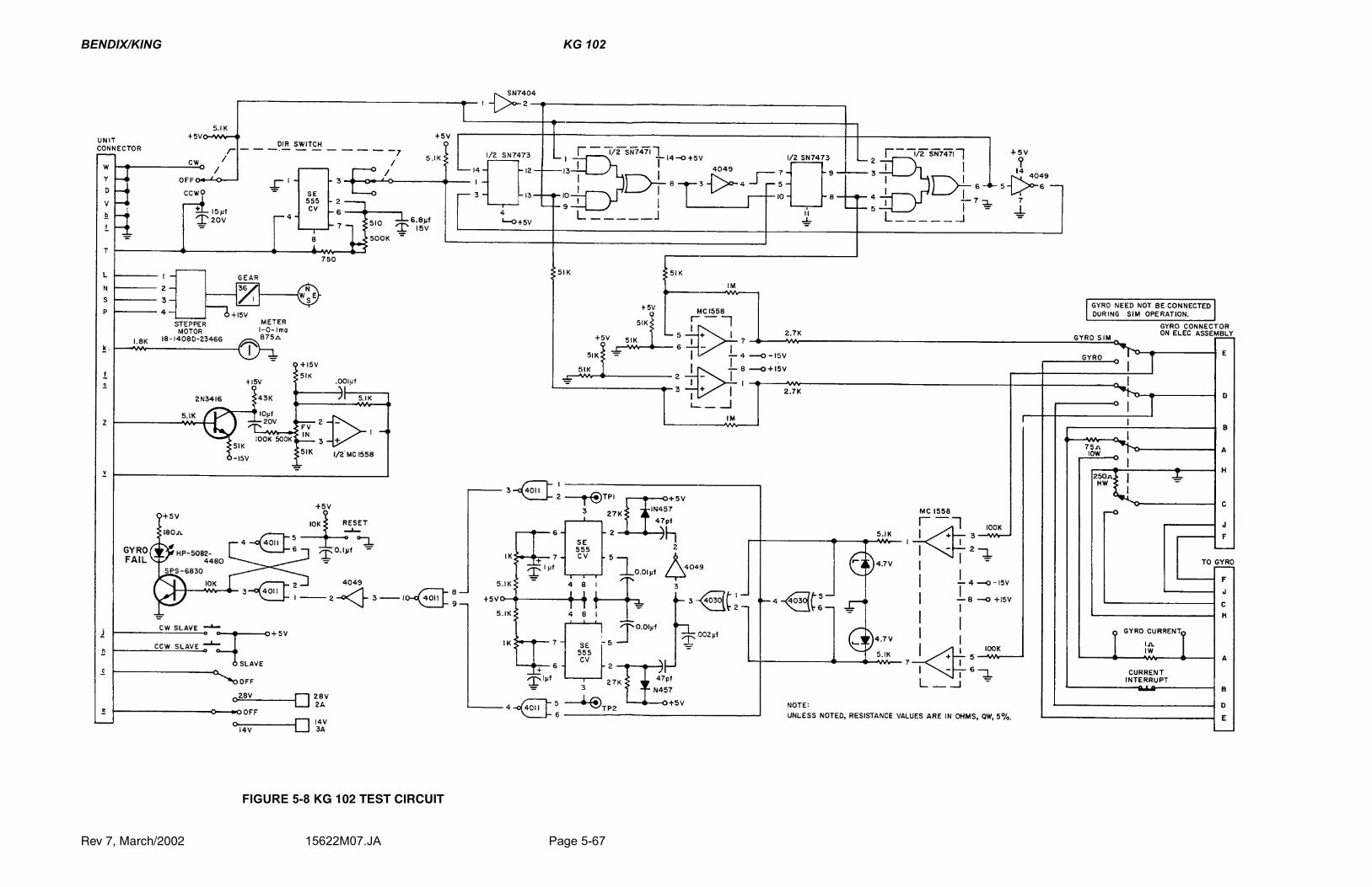
BENDIX/KING KG 102
Rev 7, March/2002 15622M07.JA Page 5-67
FIGURE 5-8 KG 102 TEST CIRCUIT

BENDIX/KING KG 102
Rev 7, March/2002 15622M07.JA Page 6-1
ILLUSTRATED PARTS LIST
6.1 General
The Illustrated Parts List (IPL) is a complete list of assemblies and parts required for the unit. The IPL also provides for the proper identification of replacement parts. Individual parts lists within this IPL are arranged in numerical sequence starting with the top assembly and continuing with the sub-assemblies. All me-chanical parts will be separated from the electrical parts used on the sub-assembly. Each parts list is followed by a component location drawing.
Parts identified in this IPL by Honeywell part number meet design specifications for this equipment and are the recommended replacement parts. Warranty informa-tion concerning Honeywell replacement parts is contained in Service Memo #1, P/N 600-08001-00XX.
Some part numbers may not be currently available. Consult the current Honeywell catalog or contact a Honeywell representative for equipment availability.
6.2 Revision Service
The manual will be revised as necessary to reflect current information.
6.3 List of Abbreviations
Abbreviation Name
B Motor or Synchro
C Capacitor
CJ Circuit Jumper
CR Diode
DS Lamp
E Voltage or Signal Connect Point
F Fuse
FL Filter
FT Feedthru
I Integrated Circuit
J Jack or Fixed Connector
L Inductor
M Meter
P Plug
Table 1 Abbreviations
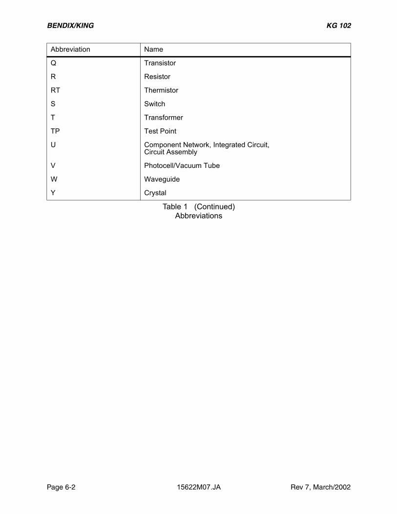
BENDIX/KING KG 102
Page 6-2 15622M07.JA Rev 7, March/2002
Q Transistor
R Resistor
RT Thermistor
S Switch
T Transformer
TP Test Point
U Component Network, Integrated Circuit,Circuit Assembly
V Photocell/Vacuum Tube
W Waveguide
Y Crystal
Abbreviation Name
Table 1 (Continued) Abbreviations

BENDIX/KING KG 102
Rev 7, March/2002 15622M07.JA Page 6-3
6.4 Sample Parts List
The above is only a sample. The actual format and style may vary slightly. A ‘Find Number’ column, when shown, references selected items on the BOM’s accompa-nying Assembly Drawing. This information does not apply to every BOM. There-fore, a lack of information in this column, or a lack of this column, should not be interpreted as an omission.
Figure 6-1 Sample Parts List

BENDIX/KING KG 102
Page 6-4 15622M07.JA Rev 7, March/2002
THIS PAGE IS RESERVED
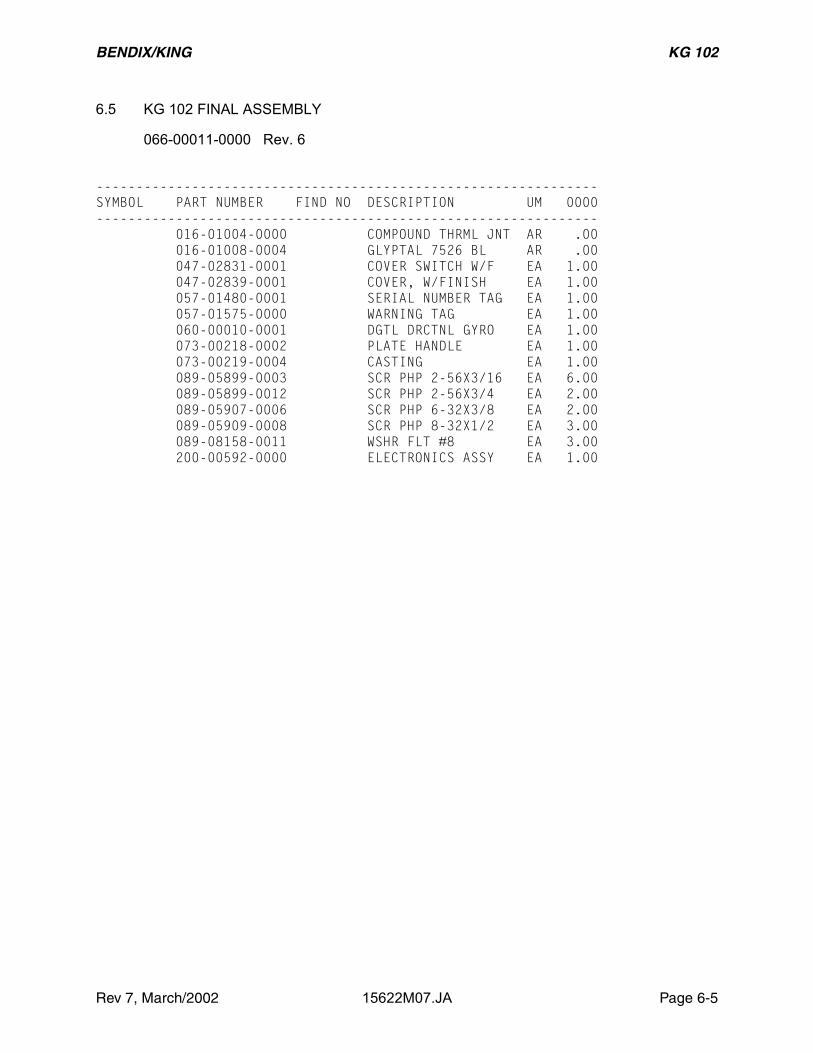
BENDIX/KING KG 102
Rev 7, March/2002 15622M07.JA Page 6-5
6.5 KG 102 FINAL ASSEMBLY
066-00011-0000 Rev. 6
---------------------------------------------------------------SYMBOL PART NUMBER FIND NO DESCRIPTION UM 0000--------------------------------------------------------------- 016-01004-0000 COMPOUND THRML JNT AR .00 016-01008-0004 GLYPTAL 7526 BL AR .00 047-02831-0001 COVER SWITCH W/F EA 1.00 047-02839-0001 COVER, W/FINISH EA 1.00 057-01480-0001 SERIAL NUMBER TAG EA 1.00 057-01575-0000 WARNING TAG EA 1.00 060-00010-0001 DGTL DRCTNL GYRO EA 1.00 073-00218-0002 PLATE HANDLE EA 1.00 073-00219-0004 CASTING EA 1.00 089-05899-0003 SCR PHP 2-56X3/16 EA 6.00 089-05899-0012 SCR PHP 2-56X3/4 EA 2.00 089-05907-0006 SCR PHP 6-32X3/8 EA 2.00 089-05909-0008 SCR PHP 8-32X1/2 EA 3.00 089-08158-0011 WSHR FLT #8 EA 3.00 200-00592-0000 ELECTRONICS ASSY EA 1.00

BENDIX/KING KG 102
Page 6-6 15622M07.JA Rev 7, March/2002
THIS PAGE IS RESERVED

BENDIX/KING KG 102
Rev 7, March/2002 15622M07.JA Page 6-7
FIGURE 6-2 KG 102 FINAL ASSEMBLY DRAWING(Dwg. 300-00797-0000 Rev. 5)

BENDIX/KING KG 102
Rev 7, March/2002 15622M07.JA Page 6-9
FIGURE 6-2A KG 102 FINAL ASSEMBLY(Dwg. 300-00797-0000 Original Revision)

BENDIX/KING KG 102
Rev 7, March/2002 15622M07.JA Page 6-11
6.6 KG 102 ELECTRONIC ASSEMBLY
200-00592-0000 Rev. 7
---------------------------------------------------------------SYMBOL PART NUMBER FIND NO DESCRIPTION UM 0000--------------------------------------------------------------- 007-00115-0000 XSTR S NPN 2N5037 EA 2.00 007-00184-0000 XSTR 2N6179/HDWR EA 4.00 007-00184-0001 XSTR 2N6181/HDWR EA 1.00 008-00022-0000 SOLDER LUG EA 2.00 016-01004-0000 COMPOUND THRML JNT AR .00 016-01008-0004 GLYPTAL 7526 BL AR .00 019-07048-0000 XFMR INV OUT EA 1.00 025-00003-0001 WIRE 22 BRN IN 3.60 025-00003-0010 WIRE 22 BK/WH IN 3.60 025-00003-0013 WIRE 22 OR/WH IN 7.20 025-00003-0014 WIRE 22 YL/WH IN 3.60 025-00018-0000 WIRE 26 BLK IN 1.20 025-00018-0011 WIRE 26 BRN IN 1.20 025-00018-0022 WIRE 26 RED IN 1.20 025-00018-0030 WIRE 26 OR/BK IN 2.40 025-00018-0040 WIRE 26 YL/BK IN 2.40 025-00018-0044 WIRE 26 YEL IN 1.20 031-00219-0000 SWITCH DPDT LOCKIN EA 1.00 047-02830-0002 CHASS POWER SUPPLY EA 1.00 089-02005-0037 NUT, STD, HEX, 2-5 EA 4.00 089-02009-0037 NUT FLAT 4-40 EA 5.00 089-02015-0037 NUT FLAT 8-32 EA 2.00 089-05460-0004 SCR, TPG, TC, 2-32 EA 4.00 089-05899-0006 SCR PHP 2-56X3/8 EA 4.00 089-05903-0003 SCR PHP 4-40X3/16 EA 2.00 089-05903-0007 SCR PHP 4-40X7/16 EA 5.00 089-06008-0004 SCR FHP 4-40X1/4 EA 2.00 089-06014-0006 SCR FHP 8-32X3/8 EA 2.00 089-08017-0037 WSHR INTL LK #8 EA 2.00 089-08023-0030 WSHR FLT STD #2 EA 4.00 089-08025-0030 WSHR FLT STD #4 EA 5.00 091-00080-0000 WASHER MICA EA 2.00 091-00109-0000 CABLE TIE EA 11.00 091-00185-0000 INSULATOR SHLDR EA 4.00 187-01029-0000 SEAL-CHANNEL IN 1.20 200-00593-0000 POWER SUPPLY BD EA 1.00 200-00594-0000 LOGIC BD EA 1.00 200-00595-0000 CABLE ASSEMBLY EA 1.00 200-01702-0000 DGTL FLTR BD ASSY EA 1.00

BENDIX/KING KG 102
Page 6-12 15622M07.JA Rev 7, March/2002
THIS PAGE IS RESERVED

BENDIX/KING KG 102
Rev 7, March/2002 15622M07.JA Page 6-13
FIGURE 6-3 KG 102 ELECTRONIC ASSEMBLY DRAWING(Dwg. 300-00793-0000 Rev. 11)

BENDIX/KING KG 102
Rev 7, March/2002 15622M07.JA Page 6-15
6.7 KG 102 POWER SUPPLY PCB ASSEMBLY
200-00593-0000 Rev. 10
---------------------------------------------------------------SYMBOL PART NUMBER FIND NO DESCRIPTION UM 0000--------------------------------------------------------------- 007-00026-0003 XSTR S NPN 2N3416 EA 4.00 007-00210-0000 XSTR S X39E1798 EA 1.00 007-05011-0000 DIO Z 6.2V 1W 5% EA 1.00 007-05011-0003 DIO Z 16V 1W 5% EA 2.00 007-06025-0000 DIO S 1N4003 EA 8.00 007-06029-0000 DIO S 1N457A EA 2.00 009-05323-0000 BOARD, PRINT CIRC EA 1.00 016-01040-0000 COATING TYPE AR AR .00 019-02174-0000 CHOKE 2.5MH EA 1.00 030-02185-0001 RGT ANG HDR 10P EA 1.00 090-00077-0000 HEAT SINK FOR T05 EA 1.00 092-05015-0002 EYE FUNN .047X.118 EA 2.00 097-00065-0000 CAP AL 500UF 50V EA 1.00 097-00066-0000 CAP AL 150UF 25V EA 3.00 105-00031-0032 CAP MY .01UF 80V EA 1.00 105-00031-0033 CAP MY .01UF 80V EA 1.00 113-05102-0000 CAP DC .001UF 500V EA 2.00 116-06104-0000 CAP DC .1UF 25V EA 3.00 120-03026-0051 IC MC78M06CG EA 1.00 120-03040-0000 IC SE555CN EA 1.00 130-00103-0023 RES FC 10K QW 5% EA 5.00 130-00202-0023 RES FC 2K QW 5% EA 4.00 130-00391-0043 RES FC 390 1W 5% EA 3.00 133-00072-0025 RES VA 250K 1W 20% EA 1.00 136-06980-0072 RES PF 698 QW 1% EA 1.00

BENDIX/KING KG 102
Page 6-16 15622M07.JA Rev 7, March/2002
THIS PAGE IS RESERVED

BENDIX/KING KG 102
Rev 7, March/2002 15622M07.JA Page 6-17
FIGURE 6-4 KG 102 POWER SUPPLY ASSEMBLY DRAWING(Dwg. 300-00794-0000 Rev. 5)

BENDIX/KING KG 102
Rev 7, March/2002 15622M07.JA Page 6-19
FIGURE 6-4A KG 102 POWER SUPPLY ASSEMBLY DRAWING(Dwg. 300-00794-0000 Manual Rev. 1 Copy)

BENDIX/KING KG 102
Rev 7, March/2002 15622M07.JA Page 6-21
FIGURE 6-4B KG 102 POWER SUPPLY ASSEMBLY DRAWING(Dwg. 300-00794-0000 Original Manual Revision Copy)

BENDIX/KING KG 102
Rev 7, March/2002 15622M07.JA Page 6-23
FIGURE 6-5 KG 102 POWER SUPPLY SCHEMATIC(Dwg. 002-00303-0002 Rev. 6)

BENDIX/KING KG 102
Rev 7, March/2002 15622M07.JA Page 6-25
FIGURE 6-5A KG 102 POWER SUPPLY SCHEMATIC(Dwg. 002-00303-0002 Rev. 1, Manual Revision 1 Copy)
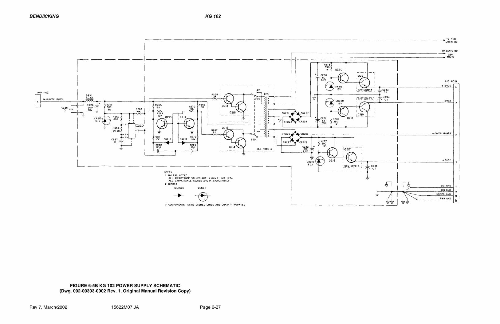
BENDIX/KING KG 102
Rev 7, March/2002 15622M07.JA Page 6-27
FIGURE 6-5B KG 102 POWER SUPPLY SCHEMATIC(Dwg. 002-00303-0002 Rev. 1, Original Manual Revision Copy)
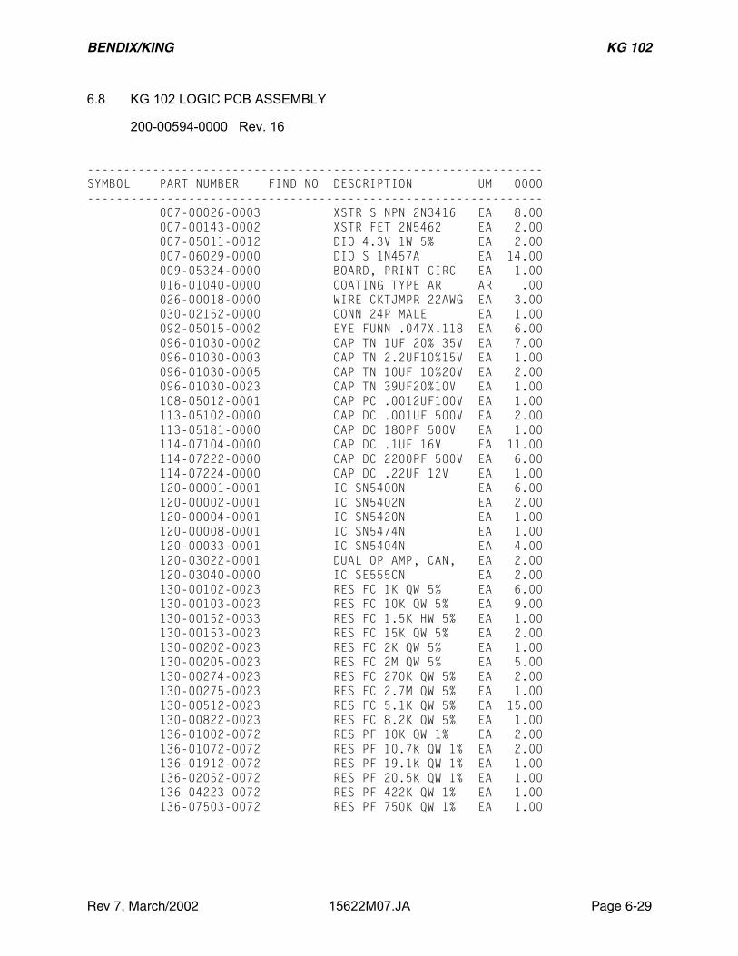
BENDIX/KING KG 102
Rev 7, March/2002 15622M07.JA Page 6-29
6.8 KG 102 LOGIC PCB ASSEMBLY
200-00594-0000 Rev. 16
---------------------------------------------------------------SYMBOL PART NUMBER FIND NO DESCRIPTION UM 0000--------------------------------------------------------------- 007-00026-0003 XSTR S NPN 2N3416 EA 8.00 007-00143-0002 XSTR FET 2N5462 EA 2.00 007-05011-0012 DIO 4.3V 1W 5% EA 2.00 007-06029-0000 DIO S 1N457A EA 14.00 009-05324-0000 BOARD, PRINT CIRC EA 1.00 016-01040-0000 COATING TYPE AR AR .00 026-00018-0000 WIRE CKTJMPR 22AWG EA 3.00 030-02152-0000 CONN 24P MALE EA 1.00 092-05015-0002 EYE FUNN .047X.118 EA 6.00 096-01030-0002 CAP TN 1UF 20% 35V EA 7.00 096-01030-0003 CAP TN 2.2UF10%15V EA 1.00 096-01030-0005 CAP TN 10UF 10%20V EA 2.00 096-01030-0023 CAP TN 39UF20%10V EA 1.00 108-05012-0001 CAP PC .0012UF100V EA 1.00 113-05102-0000 CAP DC .001UF 500V EA 2.00 113-05181-0000 CAP DC 180PF 500V EA 1.00 114-07104-0000 CAP DC .1UF 16V EA 11.00 114-07222-0000 CAP DC 2200PF 500V EA 6.00 114-07224-0000 CAP DC .22UF 12V EA 1.00 120-00001-0001 IC SN5400N EA 6.00 120-00002-0001 IC SN5402N EA 2.00 120-00004-0001 IC SN5420N EA 1.00 120-00008-0001 IC SN5474N EA 1.00 120-00033-0001 IC SN5404N EA 4.00 120-03022-0001 DUAL OP AMP, CAN, EA 2.00 120-03040-0000 IC SE555CN EA 2.00 130-00102-0023 RES FC 1K QW 5% EA 6.00 130-00103-0023 RES FC 10K QW 5% EA 9.00 130-00152-0033 RES FC 1.5K HW 5% EA 1.00 130-00153-0023 RES FC 15K QW 5% EA 2.00 130-00202-0023 RES FC 2K QW 5% EA 1.00 130-00205-0023 RES FC 2M QW 5% EA 5.00 130-00274-0023 RES FC 270K QW 5% EA 2.00 130-00275-0023 RES FC 2.7M QW 5% EA 1.00 130-00512-0023 RES FC 5.1K QW 5% EA 15.00 130-00822-0023 RES FC 8.2K QW 5% EA 1.00 136-01002-0072 RES PF 10K QW 1% EA 2.00 136-01072-0072 RES PF 10.7K QW 1% EA 2.00 136-01912-0072 RES PF 19.1K QW 1% EA 1.00 136-02052-0072 RES PF 20.5K QW 1% EA 1.00 136-04223-0072 RES PF 422K QW 1% EA 1.00 136-07503-0072 RES PF 750K QW 1% EA 1.00

BENDIX/KING KG 102
Page 6-30 15622M07.JA Rev 7, March/2002
THIS PAGE IS RESERVED

BENDIX/KING KG 102
Rev 7, March/2002 15622M07.JA Page 6-31
FIGURE 6-6 KG 102 LOGIC ASSEMBLY DRAWING(Dwg. 300-00795-0000 Rev. 8)

BENDIX/KING KG 102
Rev 7, March/2002 15622M07.JA Page 6-33
FIGURE 6-6A KG 102 LOGIC ASSEMBLY DRAWING(Dwg. 300-00795-0000 Rev. 2)
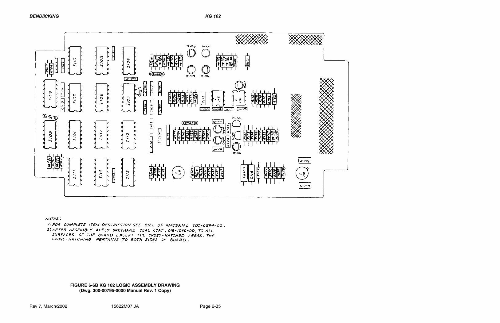
BENDIX/KING KG 102
Rev 7, March/2002 15622M07.JA Page 6-35
FIGURE 6-6B KG 102 LOGIC ASSEMBLY DRAWING(Dwg. 300-00795-0000 Manual Rev. 1 Copy)

BENDIX/KING KG 102
Rev 7, March/2002 15622M07.JA Page 6-37
FIGURE 6-6B KG 102 LOGIC ASSEMBLY DRAWING(Dwg. 300-00795-0000 Original Manual Revision Copy)

BENDIX/KING KG 102
Rev 7, March/2002 15622M07.JA Page 6-39
FIGURE 6-7 KG 102 LOGIC ASSEMBLY SCHEMATIC(Dwg. 002-00303-0001 Rev. 11)

BENDIX/KING KG 102
Rev 7, March/2002 15622M07.JA Page 6-41
FIGURE 6-7A KG 102 LOGIC ASSEMBLY SCHEMATIC(Dwg. 002-00303-0001 Rev. 1, Manual Revision 1 Copy)

BENDIX/KING KG 102
Rev 7, March/2002 15622M07.JA Page 6-43
FIGURE 6-7B KG 102 LOGIC ASSEMBLY SCHEMATIC(Dwg. 002-00303-0001 Rev. 1, Original Manual Revision Copy)

BENDIX/KING KG 102
Rev 7, March/2002 15622M07.JA Page 6-45
6.9 KG 102 CABLE ASSEMBLY
200-00595-0000 Rev. 3
---------------------------------------------------------------SYMBOL PART NUMBER FIND NO DESCRIPTION UM 0000--------------------------------------------------------------- 025-00018-0001 WIRE 26 BK/BN IN 4.80 025-00018-0011 WIRE 26 BRN IN 4.80 025-00018-0033 WIRE 26 ORG IN 4.80 025-00018-0044 WIRE 26 YEL IN 4.80 025-00018-0055 WIRE 26 GRN IN 4.80 025-00018-0088 WIRE 26 GRY IN 4.80 025-00018-0089 WIRE 26 GY/WH IN 4.80 025-05001-0000 CA 2 CNDCT REDBLK IN 4.80 030-02184-0000 CONN 9 PIN FEM EA 1.00 150-00018-0000 TUBING SHRINK 24G IN 1.20 150-00024-0010 TUBING SHRINK 10G IN 1.20 150-00060-0000 SPIROBAND IN 4.80

BENDIX/KING KG 102
Page 6-46 15622M07.JA Rev 7, March/2002
THIS PAGE IS RESERVED

BENDIX/KING KG 102
Rev 7, March/2002 15622M07.JA Page 6-47
FIGURE 6-8 KG 102 CABLE ASSEMBLY DRAWING(Dwg. 300-00796-0000 Rev. 4)
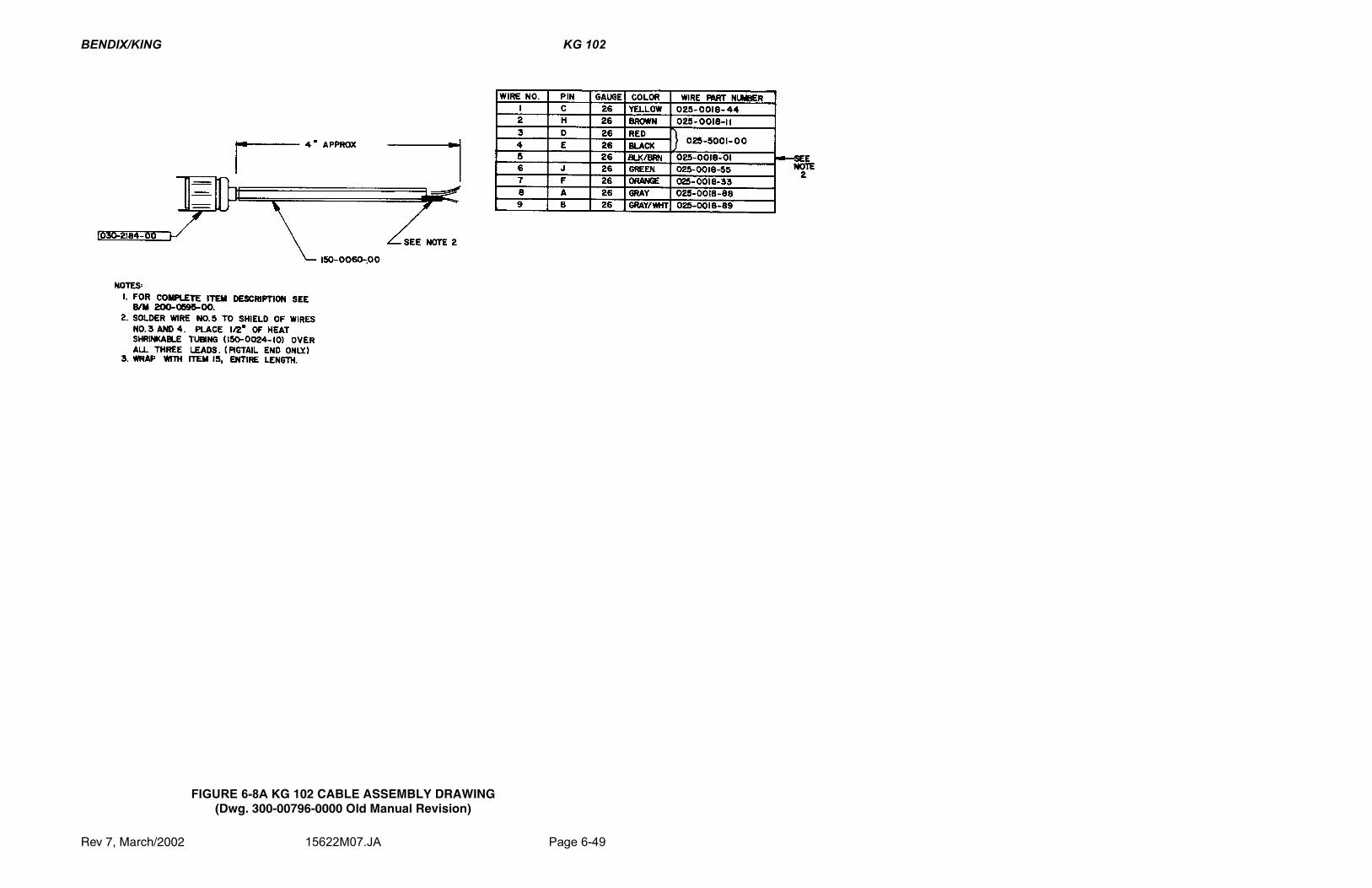
BENDIX/KING KG 102
Rev 7, March/2002 15622M07.JA Page 6-49
FIGURE 6-8A KG 102 CABLE ASSEMBLY DRAWING(Dwg. 300-00796-0000 Old Manual Revision)

BENDIX/KING KG 102
Rev 7, March/2002 15622M07.JA Page 6-51
6.10 KG 102 DIGITAL FILTER BOARD ASSEMBLY
200-01702-0000 Rev. 1
---------------------------------------------------------------SYMBOL PART NUMBER FIND NO DESCRIPTION UM 0000--------------------------------------------------------------- 007-05011-0012 DIO 4.3V 1W 5% EA 2.00 009-05674-0001 PC BD. DIGITAL EA 1.00 016-01040-0000 COATING TYPE AR AR .00 120-00008-0001 IC SN5474N EA 1.00 120-00043-0001 IC SN5486N EA 1.00 130-00242-0023 RES FC 2.4K QW 5% EA 2.00

BENDIX/KING KG 102
Page 6-52 15622M07.JA Rev 7, March/2002
THIS PAGE IS RESERVED

BENDIX/KING KG 102
Rev 7, March/2002 15622M07.JA Page 6-53
6.11 R.C. ALLEN GYRO INFORMATION
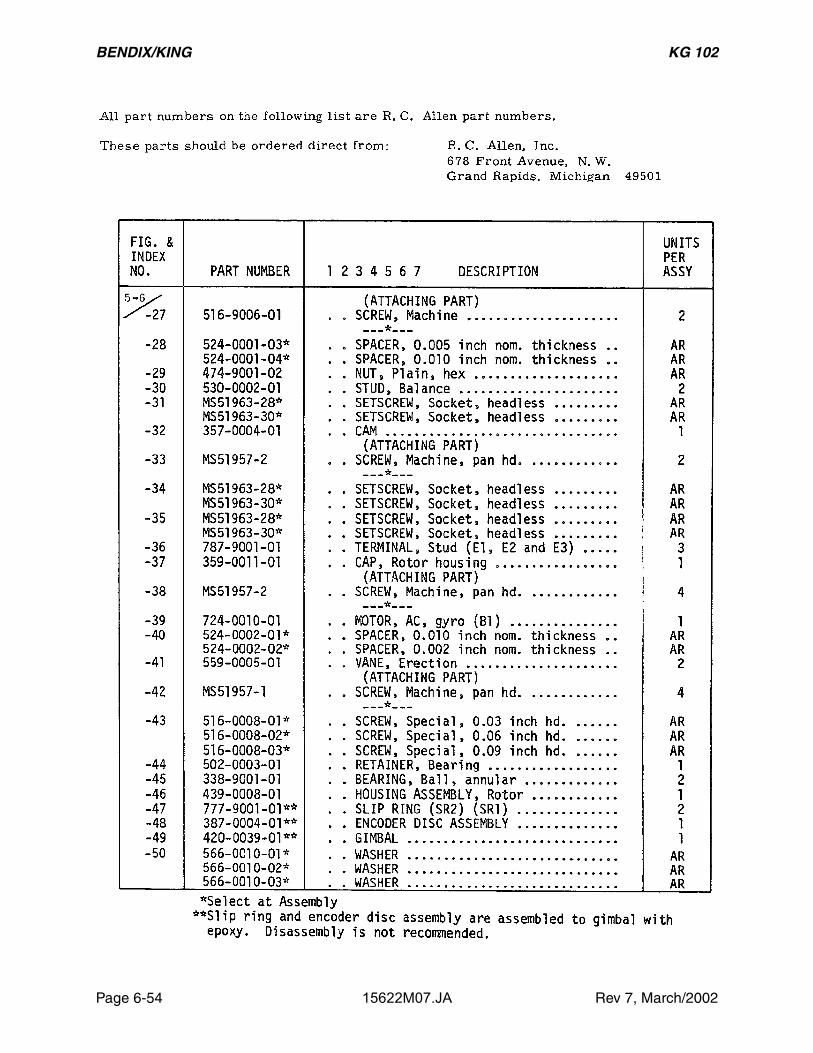
BENDIX/KING KG 102
Page 6-54 15622M07.JA Rev 7, March/2002

BENDIX/KING KG 102
Rev 7, March/2002 15622M07.JA Page 6-55

BENDIX/KING KG 102
Page 6-56 15622M07.JA Rev 7, March/2002

BENDIX/KING KG 102
Rev 7, March/2002 15622M07.JA Page 6-57
FIGURE 6-9 REMOTE GYRO ASSEMBLY(Sheet 1 of 2)

BENDIX/KING KG 102
Rev 7, March/2002 15622M07.JA Page 6-59
FIGURE 6-9 REMOTE GYRO ASSEMBLY(Sheet 2 of 2)