l = 40 nm in0.7ga0.3as mhemts - massachusetts … slides.pdf · 14 balance in f t and f max 0 200...
TRANSCRIPT

1
fT = 688 GHz and fmax = 800 GHz in
Lg = 40 nm In0.7Ga0.3As MHEMTs
with gm_max > 2.7 mS/m
D.-H. Kim, B. Brar and *J. A. del Alamo,Teledyne Scientific Company, *MIT
IEDM December-6th, 2011

III-V HEMT: record fT vs. time
2
Current record:ft=660 GHzLeuther IPRM 2011 (Fraunhofer Inst.)
(and MHEMT)
For >20 years, record fT obtained on InGaAs-channel HEMTs.
Well balanced devices:ft=644 GHz, fmax=680 GHz at same bias pointKim EDL 2010(MIT)
InGaAs-channel HEMTs offers record balanced fT and fmax.

RON ~ 420 Ohm-m
Strategy to improve fT
3
• In typical HEMTs: – RON: 350 ~ 450 Ω-m– T-Gate: Stem height = ~ 150 nm
Kim, EDL 2008
0 10 20 30 40 50 60-0.4
-0.3
-0.2
-0.1
0.0
0.1
0.2
0.3
0.4
0.5
Electron density [cm-3]
CB
Pro
file
[eV]
Vertical depth [nm]
Single delta doping
Zero bias
0
2
4
ns = 3 x 10¹² /cm2
EC and n incross section
x 1018
Lg = 30 nm
Cgext

4
Contents
1. Introduction
2. Device Technology
3. DC and RF Characteristics
4. Analytical fT Model
5. Conclusions

5
- SiO2 assisted T-gate
Lg = 40 nm Gate-stem > 250 nm
- Two-step recess (InP = 6 nm)
- Pt (3 nm)/Ti/Pt/Au Schottky
- QW: 10 nm In0.7Ga0.3As n,Hall > 10,000 cm2/V-s
- *In0.52Al0.48As/In0.7Al0.3As spacer
- **Dual Si -doping
Device Technology
S
Cap
D
Etch stopper
Barrier
Channel
Buffer
tins
OxideLside
tch
Stem
Buried Pt
100 mm InP Substrate
KIM, *Electron Lett 2011 ** IEDM 2010

6
TEM Images
- Mo-based S/D with 2 m
- Gate Stem > 250 nm
GaAs Substrate
Graded Buffer
HEMT Epi
- Lg = 40 nm, Lside = 100 nm
- tins = ~ 4 nm
Buried Pt
Ti
Pt
Au
SG
D

7
DC of Lg = 40 nm InGaAs MHEMTs
- Maximum ID > 1 mA/m- RON = 280 Ω-m
- gm > 2 mS/m @ VDS = 0.3 V- gm_max = 2.75 mS/m
@ VDS = 0.8 V
0.0 0.2 0.4 0.6 0.8 1.00.0
0.4
0.8
1.2
0.5 V
I D [m
A/
m]
VDS [V]
VGS = 0.6 V
0.0 0.2 0.4 0.60
1
2
30.8 V
0.2 V
g m [m
S/m
]
VGS [V]
VDS = 0.1 V
- Output characteristics - - gm characteristics -

-0.2 0.0 0.2 0.4 0.610-10
10-9
10-8
10-7
10-6
10-5
10-4
10-3
VDS = 0.05 V
VDS = 0.8 V ID
I D, I
G [A
/m
]
VGS [V]
IG
8
Subthreshold characteristics- Lg = 40 nm - - gm_max scalability-
gm saturates.
1001000
1500
2000
2500
3000tins = ~ 4 nm
VDS = 0.5 V
In0.7Ga0.3As MHEMTs [This work] In0.7Ga0.3As PHEMTs [IEDM-10] InAs PHEMTs [IEDM-08]
g m,m
ax [
S/m
]
Lg [nm]
- VT = 0.02 V @ VDS = 0.5 V- S = 100 mV/dec., DIBL = 105 mV/V
As Lg ↓,
This work

109 1010 1011 10120
20
40
Frequency [Hz]
Gai
ns [d
B]
0
1
2
3
4
k
Ug
MSG
Stability Factor (k)
h21
fT = 602 GHz
9
fT & fmax: Lg = 40 nm, Wg = 2 x 20 mCalibration: LRRM, De-embedding: OPEN/SHORT
- fT already approaches to 600 GHz @ VDS = 0.35 V.
- VGS/VDS = 0.4/0.35 V -
109 1010 1011 10120
20
40
Frequency [Hz]
Gai
ns [d
B]
0
1
2
3
4
fT = 688 GHz
ID = 0.4 mA/mk
Ug
MSG
Stability Factor (k)
h21
- Record fT = 688 GHz @ VDS = 0.6 V.
- VGS/VDS = 0.4/0.6 V -

Gummel technique for fT extraction
10101010
In one-pole system:
Then:
Slope gives fT
Gummel, Proc IEEE 1969
109 1010 1011 10120
20
40
Frequency [Hz]
Gai
ns [d
B]
VDS = 0.6 VID = 0.4 mA/m
k
Ug
MSG
h21
0.0 20.0G 40.0G 60.0G0.00
0.04
0.08
0.12
Imag
(h21
-1)
Frequency [Hz]
1/slope = fT= 690 GHz

11111111
109 1010 1011 10120
20
40
Frequency [Hz]
Gai
ns [d
B]
VDS = 0.6 VID = 0.4 mA/m
k
Ug
MSG
h21
Different measurement systemfor fT extraction
0.0 20.0G 40.0G 60.0G0.00
0.04
0.08
0.12
Imag
(h21
-1)
Frequency [Hz]
- 8510C @TSC: 1 ~ 50 GHz
109 1010 1011 10120
20
40
Frequency [Hz]
Gai
ns [d
B]
- PNA @UCSB: 1 ~ 67 GHz
691 GHz0.0 20.0G 40.0G 60.0G
0.00
0.04
0.08
0.12
Imag
(h21
-1)
Frequency [Hz]
1/slope = fT= 690 GHz

12
Small-signal model for fT extraction
109 1010 1011 10120
20
40
Frequency [Hz]
Gai
ns [d
B]
0
1
2
3
4
VDS = 0.6 VID = 0.4 mA/m
k
Ug
MSG
Stability Factor (k)h21
109 1010 1011 10120
20
40
Frequency [Hz]
Gai
ns [d
B]
0
1
2
3
4Stability Factor (k)
freq (1.000GHz to 67.00GHz)
S11
S21/5
S22
5xS12
- Excellent agreement, modeled fT = 680 GHzfmax = 800 GHz
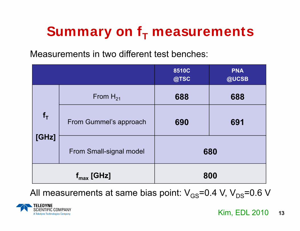
Summary on fT measurements
13131313
Measurements in two different test benches:
All measurements at same bias point: VGS=0.4 V, VDS=0.6 V
Kim, EDL 2010
8510C@TSC
PNA@UCSB
fT
[GHz]
From H21 688 688
From Gummel’s approach 690 691
From Small-signal model 680
fmax [GHz] 800

14
Balance in fT and fmax
0 200 400 600 800 10000
500
1000
1500
MIT/TSC HEMT Fujitsu HEMT NGAS HEMT SNU HEMT UCSB HBT UIUC HBT TSC HBT HRL HBT ETH HBT
max ff
f max
[GH
z]
fT [GHz]
300 600 700 = favg =
TSC/MIT(This work)
→ Best-balanced fT and fmax transistor→ Record fT FET
Lai, IEDM08Kim, IEDM10
Urteaga, DRC11

15
Contents
1. Introduction
2. Device Technology
3. DC and RF Characteristics
4. Analytical fT Model
5. Conclusions

16
Analytical fT Model
• First-order fT expression for HEMT:
gmivgs
goi
RDRS
Cgs Cgd

17
Break out ‘extrinsic’ capacitances
• Capacitance components [fF/mm]:
Cgs = Cgsi + Cgsext
= Cgsi_areal × Lg + Cgsext
Cgd = Cgdi + Cgdext
= Cgdi_areal × Lg + Cgdext
[fF/m2] [fF/m2]

18
Delay time analysis
• Delay time:
• Components of delay time:
18
Intrinsic delay (transit time)
Extrinsic delay Parasitic
delay
(Cgsi_areal + Cgdi_areal) Lggmi

19
Lg-dependent model parameters
0 100 2000
1000
2000
Cgs_ext
Cgs
, Cgd
[fF/
mm
]
Lg [nm]
VDS = 0.6 VVGS - VT = 0.3V
Cgs
Cgd
Cgd_ext
1000.1
1
10
VDS = 0.6 VVGS - VT = 0.3V
goi
Lg [nm]g m
i, goi [m
S/m
]
gmi
- Linearly proportional to Lg
- Cgs_ext > Cgd_ext
← |Vgs| < |Vgd|
- gmi saturates at Lg = ~ 60 nm- goi continues to increase
As Lg↓,
→ gmi/goi ↓
1
Cgsi_areal
20
Delay components of Lg=40 nm InGaAs MHEMT
20
Delay time from ft: ~231 fs• Intrinsic delay: ~81 fs• Extrinsic delay: ~ 99 fs• Parasitic delay: ~50 fs• Unaccounted: ~9 fs
least significant, yields ve=5 x107 cm/s
most significant
42.08%2.52%
33.84%
21.56%
accounted
Transit
ext
par
34 %
42 %
22 %
2 %

21
Scaling of delay components
0 100 2000
200
400
600VDS = 0.6 VVGS - VT = 0.3V
Del
ays
[fs]
Lg [nm]
Transit
ext
par
ext and par do not scale, become dominant for Lg < ~ 60 nm.
100
200
400
600
800
1000
VDS = 0.6 V VDS = 0.5 V VDS = 0.4 V
f T [GH
z]
Lg [nm]

• Intrinsic delay:
Lg ↓ (without degrading gmi), ve ↑ channel engineering
• Extrinsic delay:
Cgsext, Cgdext ↓, or alternatively gmi ↑ (harmonious scaling)
22
Options to improve fT
22
• Parasitic delay:
RS+RD ↓, increase electrostatic integrity: goi/gmi↓
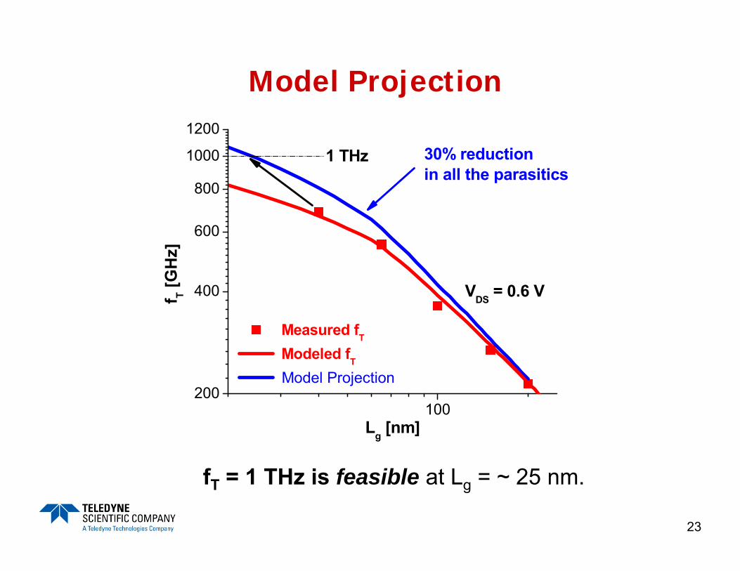
23
100200
400
600
800
1000
1200
VDS = 0.6 V
30% reductionin all the parasitics
Measured fT
Modeled fT
Model Projection
f T [GH
z]
Lg [nm]
1 THz
Model Projection
fT = 1 THz is feasible at Lg = ~ 25 nm.

24
Summary
40-nm In0.7Ga0.3As MHEMTs on GaAs substrate
- RON = 280 Ω-m, gm_max > 2.7 mS/m @ VDS = 0.8 V
- S = 100 mV/dec., DIBL = 105 mV/V
- Measured fT = 688 GHz (Record in any FET)
- fT/fmax = 688/800 GHz (Best-balanced transistor)
Analytical fT Model- Excellent description of fT behavior in III-V HEMTs
- Guidance to improve fT beyond 1 THz