l2: combinational logic design (construction and · pdf file · 2017-12-28l2:...
TRANSCRIPT

L2: 6.111 Spring 2006 1Introductory Digital Systems Laboratory
L2: Combinational Logic Design L2: Combinational Logic Design
(Construction and Boolean Algebra)(Construction and Boolean Algebra)
Acknowledgements:
Materials in this lecture are courtesy of the following sources and are used with permission.
Prof. Randy Katz (Unified Microelectronics Corporation Distinguished Professor in ElectricalEngineering and Computer Science at the University of California, Berkeley) and Prof. GaetanoBorriello (University of Washington Department of Computer Science & Engineering) from Chapter 2of R. Katz, G. Borriello. Contemporary Logic Design. 2nd ed. Pentice-Hall/Pearson Education, 2005.
J. Rabaey, A. Chandrakasan, B. Nikolic. Digital Integrated Circuits: A Design Perspective.Prentice Hall/Pearson, 2003.

L2: 6.111 Spring 2006 2Introductory Digital Systems Laboratory
Review: Noise Margin Review: Noise Margin
IN OUT IN OUT
0 1
1 0
V(x)
V(y)
VOH
VOL
VIHV
IL
Slope = -1
Slope = -1
VOLVOH
"1"
"0"
VOHVIH
VILVOL
UndefinedRegion
Large noise margins protect against various noise sources
NML= VIL -VOLNMH= VOH -VIH
Truth Table

L2: 6.111 Spring 2006 3Introductory Digital Systems Laboratory
MOS Technology: The NMOS SwitchMOS Technology: The NMOS Switch
D
G
S
gate
N+P-substrate
N+
drainsource
RNMOSSwitchModel
VT = 0.5V
VGS < VT
OFF RNMOS
VGS > VT
ON
Vs
NMOS ON when Switch Input is High
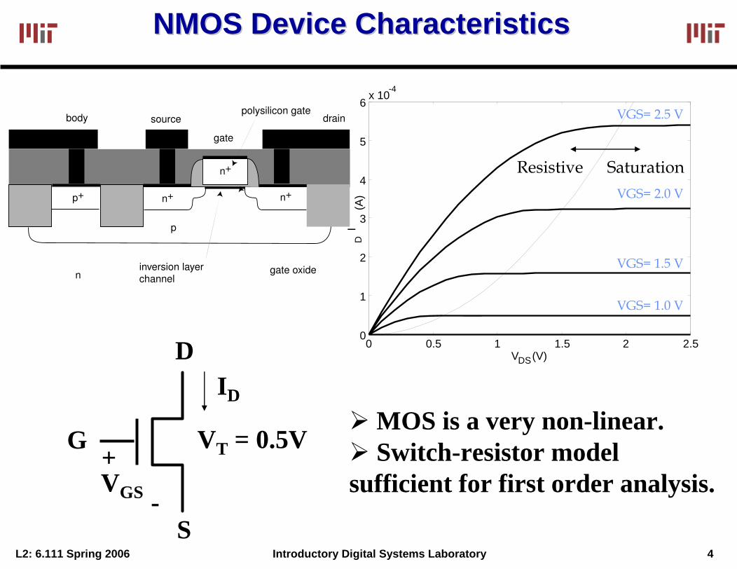
L2: 6.111 Spring 2006 4Introductory Digital Systems Laboratory
NMOS Device Characteristics NMOS Device Characteristics
0 0.5 1 1.5 2 2.50
VGS= 1.0 V
VDS(V)D
G VT = 0.5V
IDMOS is a very non-linear.
+ Switch-resistor model VGS sufficient for first order analysis.
-
1
2
3
4
5
6
D(A
)
VGS= 2.5 V
VGS= 2.0 V
VGS= 1.5 V
Resistive Saturation
x 10-4
I
S
polysilicon gatebody source drain
gate
p
p+ n+ n+
n+
inversion layer� gate oxide n channel

L2: 6.111 Spring 2006 5Introductory Digital Systems Laboratory
PMOS: The Complementary SwitchPMOS: The Complementary Switch
S
G
D
gate
P+N-substrate
P+
drainsource
RPMOSSwitchModel
VT = -0.5V
VGS > VT
OFF RPMOS
VGS < VT
ON
PMOS ON when Switch Input is Low
VDD

L2: 6.111 Spring 2006 6Introductory Digital Systems Laboratory
The CMOS InverterThe CMOS Inverter
IN OUT
VDDVDD
OUT
RPMOS
RNMOS
IN
IN
Switch Model
S
G
G
D
D
S
Rail-to-rail Swing in CMOS

L2: 6.111 Spring 2006 7Introductory Digital Systems Laboratory
Inverter VTC: Load Line AnalysisInverter VTC: Load Line Analysis
IN OUT
VDD
SG
D
D
SG
IDn
Vout
Vin = 2.5
Vin = 2
Vin = 1.5
Vin = 0
Vin = 0.5
Vin = 1
NMOS
Vin = 0
Vin = 0.5
Vin = 1Vin = 1.5
Vin = 2
Vin = 2.5
Vin = 1Vin = 1.5
PMOS
0 0.5 1 1.5 2 2.50
0.5
1
1.5
2
2.5
Vin
(V)
Vou
t(V)CMOS gates have:
Rail-to-rail swing (0V to VDD)Large noise margins“zero” static power dissipation

L2: 6.111 Spring 2006 8Introductory Digital Systems Laboratory
Possible Function of Two InputsPossible Function of Two Inputs
X
YF
X Y 16 possible functions (F0–F15)
0 0 0 0 0 0 0 0 0 0 1 1 1 1 1 1 1 10 1 0 0 0 0 1 1 1 1 0 0 0 0 1 1 1 11 0 0 0 1 1 0 0 1 1 0 0 1 1 0 0 1 11 1 0 1 0 1 0 1 0 1 0 1 0 1 0 1 0 1
X Y
X NOR YNOT (X OR Y)
X NAND YNOT (X AND Y)
10 NOT XX AND Y
X OR Y
NOT YX XOR Y X = Y
There are 16 possible functions of 2 input variables:
In general, there are 2 (2^n) functions of n inputs

L2: 6.111 Spring 2006 9Introductory Digital Systems Laboratory
Common Logic GatesCommon Logic Gates
XY Z
ZXY
X Y Z
0011
0 11 10 11 0
NAND
Gate Symbol Truth-Table Expression
X Y Z
0011
0 11 00 01 0
NOR
Z = X • Y
Z = X + Y
ZXY
X Y Z
0011
0 01 10 11 1
OR Z = X + Y
XY Z
X Y Z
0011
0 01 00 01 1
ANDZ = X • Y

L2: 6.111 Spring 2006 10Introductory Digital Systems Laboratory
Exclusive (N)OR GateExclusive (N)OR Gate
XY Z
ZXY
X Y Z
0011
0 01 10 11 0
X Y Z
0011
0 11 00 01 1
XOR(X ⊕ Y)
XNOR
(X ⊕ Y)
Widely used in arithmetic structures such as adders and multipliers
Z = X Y + X YX or Y but not both
("inequality", "difference")
Z = X Y + X YX and Y the same
("equality")

L2: 6.111 Spring 2006 11Introductory Digital Systems Laboratory
Generic CMOS RecipeGeneric CMOS RecipeVdd
A1F(A1,…,An)
pullup: make this connectionwhen we want F(A1,…,An) = 1
pulldown: make this connectionwhen we want F(A1,…,An) = 0
An
...
......
A
B
A B PDN PUN O0 0 0ff 0n 10 1 0ff 0n 11 0 0ff 0n 11 1 0n 0ff 0
B
A
CL
PUN
PDN
How do you build a 2-input NOR Gate?
AB
Note: CMOS gates result in inverting functions!(easier to build NAND vs. AND)
O

L2: 6.111 Spring 2006 12Introductory Digital Systems Laboratory
Theorems of Boolean Algebra (I)Theorems of Boolean Algebra (I)
Elementary1. X + 0 = X 1D. X • 1 = X2. X + 1 = 1 2D. X • 0 = 03. X + X = X 3D. X • X = X4. (X) = X5. X + X = 1 5D. X • X = 0
Commutativity:6. X + Y = Y + X 6D. X • Y = Y • X
Associativity:7. (X + Y) + Z = X + (Y + Z) 7D. (X • Y) • Z = X • (Y • Z)
Distributivity:8. X • (Y + Z) = (X • Y) + (X • Z) 8D. X + (Y • Z) = (X + Y) • (X + Z)
Uniting:9. X • Y + X • Y = X 9D. (X + Y) • (X + Y) = X
Absorption:10. X + X • Y = X 10D. X • (X + Y) = X11. (X + Y) • Y = X • Y 11D. (X • Y) + Y = X + Y

L2: 6.111 Spring 2006 13Introductory Digital Systems Laboratory
Theorems of Boolean Algebra (II)Theorems of Boolean Algebra (II)
Factoring:12. (X • Y) + (X • Z) = 12D. (X + Y) • (X + Z) =
X • (Y + Z) X + (Y • Z)
Consensus:13. (X • Y) + (Y • Z) + (X • Z) = 13D. (X + Y) • (Y + Z) • (X + Z) =
X • Y + X • Z (X + Y) • (X + Z)
De Morgan's:14. (X + Y + ...) = X • Y • ... 14D. (X • Y • ...) = X + Y + ...
Generalized De Morgan's:15. f(X1,X2,...,Xn,0,1,+,•) = f(X1,X2,...,Xn,1,0,•,+)
DualityDual of a Boolean expression is derived by replacing • by +, + by •, 0
by 1, and 1 by 0, and leaving variables unchangedf (X1,X2,...,Xn,0,1,+,•) ⇔ f(X1,X2,...,Xn,1,0,•,+)

L2: 6.111 Spring 2006 14Introductory Digital Systems Laboratory
Simple Example: One Bit AdderSimple Example: One Bit Adder
1-bit binary adderinputs: A, B, Carry-inoutputs: Sum, Carry-out
AB
CinCout
S
A B Cin S Cout
0 0 00 0 10 1 00 1 11 0 01 0 11 1 01 1 1
01101001
00010111
Sum-of-Products Canonical Form
S = A B Cin + A B Cin + A B Cin + A B Cin
Cout = A B Cin + A B Cin + A B Cin + A B Cin
Product term (or minterm)ANDed product of literals – input combination for which output is trueEach variable appears exactly once, in true or inverted form (but not both)

L2: 6.111 Spring 2006 15Introductory Digital Systems Laboratory
Simplify Boolean ExpressionsSimplify Boolean Expressions
Cout = A B Cin + A B Cin + A B Cin + A B Cin
= A B Cin + A B Cin + A B Cin + A B Cin + A B Cin + A B Cin
= (A + A) B Cin + A (B + B) Cin + A B (Cin + Cin)
= B Cin + A Cin + A B
= (B + A) Cin + A B
S = A B Cin + A B Cin + A B Cin + A B Cin
=( A B + A B )Cin + (A B + A B) Cin
=(A ⊕ B) Cin + (A ⊕ B) Cin= A ⊕ B ⊕ Cin

L2: 6.111 Spring 2006 16Introductory Digital Systems Laboratory
SumSum--ofof--Products & ProductProducts & Product--ofof--Sum Sum
short-hand notation form in terms of 3 variables
A B C minterms0 0 0 A B C m00 0 1 A B C m10 1 0 A B C m20 1 1 A B C m31 0 0 A B C m41 0 1 A B C m51 1 0 A B C m61 1 1 A B C m7
F in canonical form:F(A, B, C) = Σm(1,3,5,6,7)
= m1 + m3 + m5 + m6 + m7
canonical form ≠ minimal formF(A, B, C) = A B C + A B C + AB C + ABC + ABC
= (A B + A B + AB + AB)C + ABC = ((A + A)(B + B))C + ABC = C + ABC = ABC + C = AB + C
Product term (or minterm): ANDed product of literals – input combination for which output is true
F = + A B C+ A B C + A B C + ABCA B C
A B C maxterms0 0 0 A + B + C M00 0 1 A + B + C M10 1 0 A + B + C M20 1 1 A + B + C M31 0 0 A + B + C M41 0 1 A + B+ C M51 1 0 A + B +C M61 1 1 A +B + C M7
short-hand notation for maxterms of 3 variables
F in canonical form:F(A, B, C) = ΠM(0,2,4)
= M0 • M2 • M4= (A + B + C) (A + B + C) (A + B + C)
canonical form ≠ minimal formF(A, B, C) = (A + B + C) (A + B + C) (A + B + C)
= (A + B + C) (A + B + C)(A + B + C) (A + B + C)
= (A + C) (B + C)
Sum term (or maxterm) - ORed sum of literals – input combination for which output is false

L2: 6.111 Spring 2006 17Introductory Digital Systems Laboratory
Mapping Between FormsMapping Between Forms
1. Minterm to Maxterm conversion:rewrite minterm shorthand using maxterm shorthandreplace minterm indices with the indices not already used
E.g., F(A,B,C) = Σm(3,4,5,6,7) = ΠM(0,1,2)
2. Maxterm to Minterm conversion:rewrite maxterm shorthand using minterm shorthandreplace maxterm indices with the indices not already used
E.g., F(A,B,C) = ΠM(0,1,2) = Σm(3,4,5,6,7)
3. Minterm expansion of F to Minterm expansion of F':in minterm shorthand form, list the indices not already used in F
E.g., F(A,B,C) = Σm(3,4,5,6,7) F'(A,B,C) = Σm(0,1,2)= ΠM(0,1,2) = ΠM(3,4,5,6,7)
4. Minterm expansion of F to Maxterm expansion of F':rewrite in Maxterm form, using the same indices as F
E.g., F(A,B,C) = Σm(3,4,5,6,7) F'(A,B,C) = ΠM(3,4,5,6,7)= ΠM(0,1,2) = Σm(0,1,2)

L2: 6.111 Spring 2006 18Introductory Digital Systems Laboratory
The Uniting TheoremThe Uniting Theorem
A B F
0 0 1
0 1 0
1 0 1
1 1 0
B has the same value in both on-set rows– B remains
A has a different value in the two rows– A is eliminated
F = A B +AB = (A +A)B = B
Key tool to simplification: A (B + B) = AEssence of simplification of two-level logic
Find two element subsets of the ON-set where only one variable changes its value – this single varying variable can be eliminated and a single product term used to represent both elements

L2: 6.111 Spring 2006 19Introductory Digital Systems Laboratory
Boolean CubesBoolean Cubes
1-cubeX
0 1
Just another way to represent truth tableVisual technique for identifying when the uniting theorem can be appliedn input variables = n-dimensional "cube"
2-cube
X
Y
11
00
01
10
WXYZ
0111 0011
0010
0000
0001
0110
1010
0101
0100 1000
1011
1001
1110
1111
1101
1100 Y
Z W
X 3-cube
XYZ
X
011
010
000
001
111
110
100
101 Y Z
4-cube
XY

L2: 6.111 Spring 2006 20Introductory Digital Systems Laboratory
A B F
0 0 1
0 1 0
1 0 1
1 1 0
ON-set = solid nodesOFF-set = empty nodes
Circled group of the on-set is called theadjacency plane. Each adjacency plane corresponds to a product term.
A varies within face, B does notthis face represents the literal B
Mapping Truth Tables onto Boolean CubesMapping Truth Tables onto Boolean CubesUniting theorem
A
B
11
00
01
10
F
A B Cin Cout0 0 0 00 0 1 00 1 0 00 1 1 11 0 0 01 0 1 11 1 0 11 1 1 1
Cout = BCin+AB+ACin
A(B+B)CinThe on-set is completely covered by the combination (OR) of the subcubes of lower dimensionality - note that “111” is covered three times
A
B C
000
111
101
(A+A)BCin AB(Cin+Cin)
Three variable example: Binary full-adder carry-out logic

L2: 6.111 Spring 2006 21Introductory Digital Systems Laboratory
Higher Dimension CubesHigher Dimension Cubes
F(A,B,C) = Σm(4,5,6,7)on-set forms a squarei.e., a cube of dimension 2 (2-D adjacency plane)represents an expression in one variable i.e., 3 dimensions – 2 dimensionsA is asserted (true) and unchangedB and C vary
This subcube represents the literal AA
B C
000
111
101
100
001010
011110
In a 3-cube (three variables):0-cube, i.e., a single node, yields a term in 3 literals1-cube, i.e., a line of two nodes, yields a term in 2 literals2-cube, i.e., a plane of four nodes, yields a term in 1 literal3-cube, i.e., a cube of eight nodes, yields a constant term "1"
In general,m-subcube within an n-cube (m < n) yields a term with n – m literals

L2: 6.111 Spring 2006 22Introductory Digital Systems Laboratory
KarnaughKarnaugh MapsMaps
A B F0 0 10 1 01 0 11 1 0
Alternative to truth-tables to help visualize adjacenciesGuide to applying the uniting theorem - On-set elements with only one variable changing value are adjacent unlike in a linear truth-table
0 2
1 3
0 1A
B0
1
1
0 0
1
Numbering scheme based on Gray–codee.g., 00, 01, 11, 10 (only a single bit changes in code for adjacent map cells)
A B 0 1
0
1
0
1
2
3
0
1
2
3
6
7
4
5
AB C
0
1
3
2
4
5
7
6
12
13
15
14
8
9
11
10
A
B
AB CD
A
00 01 11 10
0
1
00 01 11 10
00
01
11
10 C
B
D
2-variableK-map
3-variableK-map
4-variableK-map

L2: 6.111 Spring 2006 23Introductory Digital Systems Laboratory
KK--Map ExamplesMap Examples
Cout = F(A,B,C) =
A B A
B
Cin 00 01 11 10
0
1
0
0
0
1
1
1
0
1
AB C
A
00 01 11 10
0
1
0
0
0
0
1
1
1
1
B
F(A,B,C) = Σm(0,4,5,7)
F =
00 C AB
01 11 10
1 0 0 1
1 1 0 0
A
B
0
1
00 C AB
01 11 10
0 1 1 0
0 0 1 1
A
B
0
1
F' simply replace 1's with 0's and vice versa
F'(A,B,C) = Σm(1,2,3,6)
F' =

L2: 6.111 Spring 2006 24Introductory Digital Systems Laboratory
Four Variable Four Variable KarnaughKarnaugh MapMap
F(A,B,C,D) = Σm(0,2,3,5,6,7,8,10,11,14,15)
F = C + A B D + B D
K-map Corner AdjacencyIllustrated in the 4-Cube
Find the smallest numberof the largest possible
subcubes that cover theON-set
AB 00 01 11 10
1 0 0 1
0 1 0 0
1 1 1 1
1 1 1 1
00
01
11
10 C
CD
A
D
B
0011
D
0010
0000
0111
0110
0001 C
A
B 0100 1000
1100
1101
1111
1110
1001
1011
1010
0101

L2: 6.111 Spring 2006 25Introductory Digital Systems Laboratory
KK--Map Example: DonMap Example: Don’’t Carest Cares
F(A,B,C,D) = Σm(1,3,5,7,9) + Σd(6,12,13)
F = A D + B C D w/o don't cares
F = C D + A D w/ don't cares
Don't Cares can be treated as 1's or 0's if it is advantageous to do soDon't Cares can be treated as 1's or 0's if it is advantageous to do so
By treating this DC as a "1", a 2-cubecan be formed rather than one 0-cube
AB 00 01 11 10
0 0 X 0
1 1 X 1
1 1 0 0
0 X 0 0
00
01
11
10 C
CD
A
D
B AB 00 01 11 10
0 0 X 0
1 1 X 1
1 1 0 0
0 X 0 0
00
01
11
10 C
CD
A
D
B
In PoS form: F = D (A + C)
Equivalent answer as above, but fewer literals

L2: 6.111 Spring 2006 26Introductory Digital Systems Laboratory
HazardsHazards
Figure by MIT OpenCourseWare.
A
C
B
A = B = 1
C12F
Gate delayGlitch
F
Static hazards: Consider this function:
Implemented with MSI gates:
'00'00
'00'00
A
C
B
F
2
1
CAB
00 01 11 10
0 0 0
0 0
1 1
111
F = A * C + B * C

L2: 6.111 Spring 2006 27Introductory Digital Systems Laboratory
Fixing HazardsFixing Hazards
In general, it is difficult to avoid hazards – need a robustdesign methodology to deal with hazards.
The glitch is the result of timing differences in parallel data paths. It is associated with thefunction jumping between groupings or productterms on the K-map. To fix it, cover it up withanother grouping or product term!
Figure by MIT OpenCourseWare.
CAB
00 01 11 10
0 0 0
0 0
1 1
111
A
CB
F
F = A * C + B * C + A * B