lab manual - godavaricoejal.ac.in · q3. explain the address capability of 8085 is 64 kb ans....
TRANSCRIPT

GF’s Godavari College of Engineering, Jalgaon.
Microprocessor Manual
1
GF’s Godavari College of Engineering, Jalgaon.
Dept. of Electronics & Telecommunication Engineering
Lab Manual
Microprocessor SE.SEM I
Prepared by R. V. Patil ( Asso. Prof.)

GF’s Godavari College of Engineering, Jalgaon.
Microprocessor Manual
2
Microprocessor Lab
LAB COURSE OUTLINE
Course Title Short Title & Course Code
Microprocessor Lab MP LAB
i
Course Description:
This course is designed to teach students the practical aspects of principles, interfacing and applications of microprocessor architecture, including both hardware and basic assembly language programming using the 8085 Microprocessor.
Laboratory Hours per Week No. Of Weeks Total Hours Semester Credits
2 14 28 1
Total Semester Credits: 1
Prerequisite Course(s): Digital Electronics.

GF’s Godavari College of Engineering, Jalgaon.
Microprocessor Manual
3
LAB COURSE CONTENT
(Note: Minimum Eight from List)
1 Addition of two 8 bit numbers. Performing simple arithmetic operations of addition
using 8085 Microprocessor.
2 Subtraction of two 8 bit numbers.Performing simple arithmetic operations of subtraction using 8085 Microprocessor.
3 Addition of two 16 bit numbers.Performing simple arithmetic operations of addition
using 8085 Microprocessor.
4 Subtraction of two 16 bit numbers.
Performing simple arithmetic operations of subtraction using 8085 Microprocessor.
5 Multiplication of two 8 bit numbers.
Performing simple arithmetic operations of multiplication using 8085 Microprocessor.
6 Division of two 8 bit numbers.Performing simple arithmetic operations of division using 8085 Microprocessor.
7 Program for block transfer of data bytes.
Perform block transfer of data.
8 To find square of a number using look-up table.
9 To find largest/smallest number in array of data.
10 Arrange an array of data in ascending/descending order.
11 Program to implement decimal up/down counter.
12 BCD to Hex / Hex to BCD Conversion.
13 Interfacing of 8253/54 Timer with 8085Microprocessor and generate the square wave.
14 Case study of Microprocessor controlled temperature system / microprocessor controlled manufacturing process/ traffic signal controller. (Study only)

GF’s Godavari College of Engineering, Jalgaon.
Microprocessor Manual
4
INDEX
Sr. No. Name of Experiment Page No.
1 Addition of two 8 bit numbers. Performing simple arithmetic operations of addition using 8085 Microprocessor. a)With carry provision b) Without carry provision
2 Subtraction of two 8 bit numbers.Performing simple arithmetic operations of subtraction using 8085 Microprocessor. a)Minuend is bigger than Subtrahend .b)Result with provision of sign indication
3 Addition of two 16 bit numbers.Performing simple arithmetic operations of addition using 8085 Microprocessor.
4 Subtraction of two 16 bit numbers. Performing simple arithmetic operations of subtraction using 8085 Microprocessor.
5
Multiplication of two 8 bit numbers. Performing simple arithmetic operations of multiplication using 8085 Microprocessor.
6 Program for block transfer of data bytes. Perform block transfer of data.
7 To find largest/smallest number in array of data.
8 Arrange an array of data in ascending/descending order.
9 Case study of traffic signal controller system. (Study only)

GF’s Godavari College of Engineering, Jalgaon.
Microprocessor Manual
5
Evaluation Sheet
Sr. No.
Name of Experiment Date of Performance
Date of Checking
Grade/ Marks Remark
1 Write an assembly language programming for addition of two 8bit unsigned nos. a)With carry provision b) Without carry provision
2 Write an assembly language programming for Subtraction of two 8bit unsigned nos. a)Minuend is bigger than Subtrahend .b)Result with provision of sign indication
3 Write an assembly language programming for addition of two 16bit unsigned nos.
4
Write an assembly language programming for subtraction of two 16bit unsigned nos.
5 Write an assembly language programming for multiplication of two 8bit unsigned nos.
6 Write an assembly language programming for transferring a block of 5 unsigned nos to a specified location.
7 Write an assembly language programming for a)smallest/b)Largest no within an array of 5nos.
8 Write an assembly language programming for arranging a string of two 5bit nos.in a) Ascending/b) Descending order.
9 Case study of traffic signal controller system.(Study only)
Total Marks
Average Marks

GF’s Godavari College of Engineering, Jalgaon.
Microprocessor Manual
6
ExperimentNo.-1 Date:
Write an assembly language programming for addition of two 8bit unsigned nos.
a)With carry provision
b) Without carry provision
Objective:-
Performingsimple arithmetic operations of addition using 8085 Microprocessor.
To handle the kitof microprocessor.
Apparatus: -Expt. Kit, SMPS.
Program(for a):- Flowchart
7000 LDA 7100H
7003 MOV B,A
7004 LDA 7101H
7007 ADD B
7008 STA 7102H
700B HLT
Program& Flowchart for b):- 7000 MVI C,00H
7002 LDA 7101H
7005 MOV B,A
7006 LDA 7102H
7009 ADD B
700A JNC ahead
700D INR C
700E ahead STA 7103H
7011MOV A,C
7012 STA 7104H
7015 HLT
Aim: -Addition of two 8 bit numbers.

GF’s Godavari College of Engineering, Jalgaon.
Microprocessor Manual
7
Procedure:-
1]Draw flow chartfor the logic.
2] prepare an assembly language program with starting address 7000H
3] check the ‘Opcode’ for the instruction within the program.
4] Connect the SMPS to Microprocessor kit
5] Write the program and assign two different data.
6]Check the answer.
Given Data:-
Result:-

GF’s Godavari College of Engineering, Jalgaon.
Microprocessor Manual
8
Oral Based Questions.
Q1.How many different instructions Microprocessor 8085 have? What is an instruction set?
Ans. 8085 microprocessor has a total of 74 different instructions for performing different operations or tasks. The entire different instructions that a particular microprocessor can handle is called its instruction set.
Q2. What an instruction consists of?
Ans. An instruction consists of an operation code (called ‘opcode’) and the address of the data (called ‘operand’), on which the opcode operates.
Q3.What is meant by low level and high level languages?
Programming languages that are machine dependent are called low level languages. For example, assembly language is a low level language. On the other hand, programming languages that are machine independent are calledhigh level languages. Examples are BASIC, FORTRAN, C, ALGOL, COBOL, etc.
Q4.Differentiate between a compiler/interpreter and an assembler.
Ans.
As an example, for gadget controls and traffic signals, assembly languageprogramming is done because programs in such cases are compact and not lengthy. But for cases where large program lengths are a must, compilers/interpreters are used. Forsuch a case, although a large memory space is required, the advantage lies in very quickdebugging.
Q5.Name the special purpose registers of 8085.
The special purpose registers used in 8085 microprocessor are:
1. Accumulator register (A), 2.Program counter register (PC), 3. Status (or Flag) register, 4.Stack pointer register (SP)
Sr.No . Compiler/Interpreter Assembler 1 Debugging easier Debugging relatively tougher 2 Less efficient More efficient 3 Requires large memory space Requires less memory space

GF’s Godavari College of Engineering, Jalgaon.
Microprocessor Manual
9
ExperimentNo.-2 Date:
Write an assembly language programming for subtraction of two 8bit unsigned nos.
a) Minuend is bigger than Subtrahend
b) Result with provision of sign indication
Objective:-
Performingsimple arithmetic operations of subtraction using 8085 Microprocessor.
To handle the kit of microprocessor.
Apparatus: -Expt. Kit, SMPS.
Program for a) Flowchart for a)
7000 LDA 7100H
7003 MOV B,A
7004 LDA 7101H
7007 SUB B
7008 STA 7003H
700B HLT
Given Data:-For a)
Result:-For a)
Aim: -Subtraction of two 8 bit numbers.

GF’s Godavari College of Engineering, Jalgaon.
Microprocessor Manual
10
Program for b) Flowchart for b)
7000 MVI C,00H
7002 LXI D, (Minuend, Subtrahend)H
7005 LXI H,(Subtrahend,Minuend)H
7008 MOV A, L
7009 CMP H
700A JNC ##
700D XCHG
700E INR C
700F ## MOV A, L
7010 SUB H
7011 STA 7100H
7014 MOV A, C
7015 STA 7101H
7018 HLT
Procedure:-
1]Draw flow chartfor the logic.
2] prepare an assembly language program with starting address 7000H
3] check the ‘Opcode’ for the instruction within the program.
4] Connect the SMPS to Microprocessor kit
5] Write the program and assign two different data.
6] Check the answer.
Given Data:-For b)
Result:-For b)

GF’s Godavari College of Engineering, Jalgaon.
Microprocessor Manual
11
Oral based Questions:-
Q1.Enumarate the difference between a compiler and an interpreter.
Difference between a compiler and an interpreter lies in the generation of the machine code or object code.
A compiler reads the entire program first and then generates the corresponding object code.Whereas, an interpreter
reads an instruction at a time, produces the correspondingobject code and executes the same before it starts reading the
next instruction. A programfrom a compiler runs some 5 to 25 times faster than a program from an interpreter.
Q2. What is meant by the term ‘word’?
Ans. A collection of bits is called a word. A word does not have a fixed number of bits—unlikethe case of byte (= 8 byte)
or a nibble (= 4 bytes). For different microprocessors, the word length varies. For example, for 8-bitmicroprocessors, the
word length is 8-bits while that for 32-bit microprocessors, the wordlength is 32-bits.A word is expressed usually in
multiples of 2, but no value is excluded. That is, wecan have a 19-bit word or 37-bit word, etc.
Q3. Explain the address capability of 8085 is 64 KB
Ans. Microprocessor 8085 communicates via its address bus of 2-bytes width – the lower byteAD0– AD7 (pins 12-19) and
upper byte D8– D15 (pins 21–28). Thus it can address amaximum of 216 different address locations. Again each address
(memory location) canhold 1 byte of data/instruction. Hence the maximum address capability of 8085 is
=216 × 1 Byte
= 65, 536 × 1 Byte
= 64 KB (where 1 K = 1024 bytes)
Q4. Mention the addressing modes of 8085;Give one example each of the five types of addressing modes.
Ans. 8085 has the following addressing modes: Immediate, Register, Direct, Indirect and Implied. The examples for each
type of addressing mode are given below:
(a) Direct Addressing: In this mode, the operand is specified within the instruction itself.
Examples of this type are:LDA 4000H, STA 5513H, etc.IN/OUT instructions (like IN PORT C, OUT PORT B, etc.) also falls
under thiscategory.
(b) Register Addressing: In this mode of addressing, the operand is in the generalpurpose registers.
Examples are: MOV A, B ; ADD D, etc.
(c) Register Indirect Addressing: MOV A, M; ADD M are examples of this mode ofaddressing. These instructions utilize 1-
byte. In this mode, instead of specifying aregister, a register pair is specified to accommodate the 16-bit address of the
operand.
(d) Immediate Addressing: MVI A, 07; ADI 0F are examples of Immediate Addressingmode.The operand is specified in the
instruction in this mode. Here, the operand addressis not specified.

GF’s Godavari College of Engineering, Jalgaon.
Microprocessor Manual
12
(e) Implicit Addressing: In this mode of addressing, the operand is fully absent.
Examplesare RAR, RAL, CMA, etc.
Q5.What jobs ALU of 8085 can perform?
The Arithmetic Logic Unit (ALU) of 8085 can perform the following jobs:
1. 8-bit binary addition with or without carry.,2. 16-bit binary addition.,3. 2-digit BCD addition.,4. 8-bit binary
subtraction with or without borrow.,5. 8-bit logical OR, AND, EXOR, complement (NOT function).,6. bit shift
operation.

GF’s Godavari College of Engineering, Jalgaon.
Microprocessor Manual
13
Experiment No.-3 Date:-
Aim:-Addition of two 16 bit numbers.
Write an assembly language programming for addition of two 16bit nos.
Objective:
Performing simple arithmetic operations of addition using 8085 Microprocessor.
To handle the kit of microprocessor.
Apparatus: -Expt. Kit, SMPS.
Flowchart:-
Program:-
7000 2A,00,71 LHLD 7100H ; Load first (lower 8 bit at 7100,Higher 8 bit at 7101)in H-L pair
7003 EB XCHG ;Shift to D-E pair
7004 2A,02,71 LHLD 7102H ; Load second (lower 8 bit at 7102,Higher 8 bit at 7103)in H-L pair
7007 19 DAD D ; add both no.
7008 22,04,71 SHLD 7104H ; Save the result(lower 8 bit at 7104, Higher 8 bit at 7105) in H-L pair
700B 76 HLT ; Stop the program.

GF’s Godavari College of Engineering, Jalgaon.
Microprocessor Manual
14
Procedure:-
1]Draw flow chartfor the logic.
2] prepare an assembly language program with starting address 7000H
3] check the ‘Opcode’ for the instruction within the program.
4] Connect the SMPS to Microprocessor kit
5] Write the program and assign two different data.
6] Check the answer.
Given Data:-
Result:-
Oral Based Questions
Q.1: What are the different buses and what jobs they do in a microprocessor?
Ans.The different buses in a microprocessor are the data bus (DB), address bus (AB) and the control bus (CB). Data flow through the DB, while address comes out of the AB and CB controls the activities of the microcomputer system at any instant of time.
Q.2: Describe the (status) flag register of 8085.
Ans. It is an 8-bit register in which five bit positions contain the status of five condition flagswhich are Zero (Z), Sign (S), Carry (CY), Parity (P) and Auxiliary carry (AC). Each of these five flags is a 1 bit F/F. The flag register format is shown in Fig. 2.6:
Fig. 2.6: The flag register format

GF’s Godavari College of Engineering, Jalgaon.
Microprocessor Manual
15
1 Sign (S) flag: – If the MSB of the result of an operation is 1, this flag is set, otherwiseit is reset.
2 Zero (Z) flag: – If the result of an instruction is zero, this flag is set, otherwise reset.
3 Auxiliary Carry (AC) flag: – If there is a carry out of bit 3 and into bit 4 resulting fromthe execution of an arithmetic operation, it is set otherwise reset. This flag is used for BCD operation and is not available to the programmer to changethe sequence of an instruction.
4 Carry (CY) flag: – If an instruction results in a carry (for addition operation) or borrow(for subtraction or comparison) out of bit D7, then this flag is set, otherwise reset.
5 Parity (P) flag:– This flag is set when the result of an operation contains an even number of 1’s and is reset otherwise.
Q.3: Explain(a) Control and Status signals,(b) Interrupt signals,(c) Serial I/O signals,(d) DMA signals,(e) Reset signals.
Ans. The control and status signals are ALE, RD, WR, IO/M, S0, and S1 and READY, The interrupt signals are TRAP, RST 7.5, RST 6.5, RST 5.5, INTR. INTA is an interrupt acknowledgement signal indicating that the processor has acknowledged an INTR interrupt.Serial I/O signals are SID and SOD, DMA signals are HOLD and HLDA, and Reset signals are RESET IN and RESET OUT.
Q.4: Mention the two broad categories in which data transfer schemes are classifiedand the types of programmed data transfer.
Ans. The data transfer schemes are broadly classified into two categories. These are
a) Programmed data transfer
b)Direct Memory Access (DMA) transfer.
Programmed data transfer scheme is sub-divided into the following:
1 Synchronous mode of data transfer,2 Asynchronous mode of data transfer and 3 Interrupt driven mode of data transfer.
Q5: How many hardware interrupts 8085 supports? How many I/O ports can 8085 access? Ans. It supports five (5) hardware interrupts—TRAP, RST 7.5, RST 6.5, RST 5.5 and INTR. It provides 8-bit I/O addresses. Thus it can access 28 = 256 I/O ports.

GF’s Godavari College of Engineering, Jalgaon.
Microprocessor Manual
16
ExperimentNo:-4 Date:-
Aim:-Subtraction of two 16 bit numbers.
Write an assembly language programming for subtraction of two 16bit nos.
Objective:
Performing simple arithmetic operations of subtraction using 8085 Microprocessor.
To handle the kit of microprocessor.
Apparatus: -Expt. Kit, SMPS.
Program :- Flowchart :-
7000 LHLD 7100H
7003 XCHG
7004 LHLD 7102H
7007 MOV A, E
7008 SUB L
7009 MOV L, A
700A SBB H
700B MOV H, A
700C SHLD 7104H
700F HLT
Procedure:-
1]Draw flow chartfor the logic.
2] prepare an assembly language program with starting address 7000H
3] check the ‘Opcode’ for the instruction within the program.
4] Connect the SMPS to Microprocessor kit
5] Write the program and assign two different data.
6] Check the answer.
Given Data:-
Result:-

GF’s Godavari College of Engineering, Jalgaon.
Microprocessor Manual
17
Oral Based Questions
Q.1: Draw the Opcode Fetch machine cycle of 8085 and discuss.
Ans:-The first machine cycle of every instruction is the Opcode Fetch. This indicates the kind of instruction to
be executed by the system. The length of this machine cycle varies between 4T to 6T states—it depends on the
type of instruction. In this, the processor places the contents of the PC on the address lines, identifies the
nature of machine cycle (by IO/M, S0,S1) and activates the ALE signal. All these occur in T1 state.,
In T2 state, RD signal is activated so that the identified memory location is read from and places the content on
the data bus (D0 – D7).In T3, data on the data bus is put into the instruction register (IR) and also raises the RD
signal thereby disabling the memory.In T4, the processor takes the decision, on the basis of decoding the IR,
whether to enter into T5 and T6 or to enter T1 of the next machine cycle.One byte instructions that operate on
eight bit data are executed in T4. Examples are ADD B, MOV C, B, RRC, DCR C, etc.

GF’s Godavari College of Engineering, Jalgaon.
Microprocessor Manual
18
Q.2: Briefly describe Memory Read and Write machine cycles and show the wave-forms?
Ans. Both the Memory Read and Memory Write machine cycles are 3T states in length. InMemory Read
the contents of R/W memory (including stack also) or ROM are read while in Memory Write, it stores data into
data memory (including stack memory). As is evident from Fig. above during T2 and T3 states data from either
memory or CPU are made available in Memory Read or Memory Write machine cycles respectively. The status
signal (IO/M, S0, S1) states are complementary in nature in Memory Read and Memory Write cycles. Reading
or writing operations are performed in T2. In T3 of Memory read, data from data bus are placed into the
specified register (A,B, C, etc.) and raises RD so that memory is disabled while in T3 of Memory Write WR
signal is raised which disables the memory.
Q.3: Draw the I/O Read and I/O Write machine cycles and discuss.
Ans. I/O Read and Write machine cycles are almost similar to Memory Read and Writemachine cycles
respectively. The difference here is in the IO/ M signal status which remains 1 indicating that these machine
cycles are related to I/O operations. Thesemachine cycles take 3T states.In I/O read, data are available in T2
and T3 states, while during the same time (T2and T3) data from CPU are made available in I/O write.The I/O
read and write machine cycles are shown in following Fig.

GF’s Godavari College of Engineering, Jalgaon.
Microprocessor Manual
19
Q4. Explain the DAD instruction and draw its timing diagram.
Ans. DAD instruction adds the contents of a specified register pair to the contents of H and L. For execution of
DAD, 10 T-states are needed. Instead of having a single machine
cycle having 10 T-states, it consists of the Opcode Fetch machine cycle (4T states) and 6 extra T-states divided
into two machine cycles. These two extra machine cycles are BusIdle Machine cycles which do not involve
either memory or I/O. The timing diagram for DAD instruction is shown below:

GF’s Godavari College of Engineering, Jalgaon.
Microprocessor Manual
20
Q5. Discuss the concept of WAIT states in microprocessors.
Ans. So many times it may happen that there is speed incompatibility between microprocessor and its memory
and I/O systems. Mostly the microprocessor is having higher speed. So in a given situation, if the
microprocessor is ready to accept data from a peripheral device while there is no valid data in the device (e.g.
an ADC), then the system enters into WAIT states and the READY pin (an input pin to the microprocessor, pin
no. 35 for 8085) is put to a low state by the device. Once the device becomes ready with some valid data, it
withdraws the low state on the READY pin of 8085. Then 8085 accepts the data from the peripheral by
software instructions.

GF’s Godavari College of Engineering, Jalgaon.
Microprocessor Manual
21
Experiment No.-5 Date:-
Aim:-Multiplication of two 8bit numbers.
Write an assembly language programming for multiplication of two 8bit nos.
Objective:
Performing simple arithmetic operations of multiplication using 8085 Microprocessor.
To handle the kit of microprocessor.
Apparatus: -Expt. Kit, SMPS.
Program:-Flowchart:-
7000 LXI H, 7100H
7003 MOV E, M
7004 MVI D, 00H
7006 INX H
7007 MOV A, M
7008 LXI H, 0000H
700B MVI B, 08H
700D MultyDAD H
700E RAL
700F JNC SKIP
7012 DAD D
7013 SKIP DCR B
7014 JNZ Multy
7017 SHLD 7102H
701A HLT

GF’s Godavari College of Engineering, Jalgaon.
Microprocessor Manual
22
Procedure:-
1]Draw flow chartfor the logic.
2] prepare an assembly language program with starting address 7000H
3] check the ‘Opcode’ for the instruction within the program.
4] Connect the SMPS to Microprocessor kit
5] Write the program and assign two different data.
6] Check the answer.
Given Data:-7100: Multiplicand
7101: Multiplier
Result:-7102:Lower Byte
7103: Higher Byte

GF’s Godavari College of Engineering, Jalgaon.
Microprocessor Manual
23
Oral Based Questions
Q.1: Does 8085 have multiplication and division instructions?
Ans. No, 8085 does not have the above two instructions. It can neither multiply nor divide two 8-bit numbers. The same are executed by the processor following the process of repetitive addition or subtraction respectively.
Q.2: Explain maskable and non-maskable interrupts.
Ans. An interrupt which can be disabled by software means, is called a maskable interrupt. Thus an interrupt which cannot be masked is an unmaskable interrupt.
Q3. Which is the non-maskable interrupt for 8085?
Ans. TRAP interrupt is the non-maskable interrupt for 8085. It means that if an interruptcomes via TRAP, 8085 will have to recognize the interrupt.
Q4. Do the interrupts of 8085 have priority?
Ans. Yes, the interrupts of 8085 have their priorities fixed—TRAP interrupt has the highestpriority, followed by RST 7.5, RST 6.5, RST 5.5 and lastly INTR.
Q5. What is meant by priority of interrupts?
Ans. It means that if 8085 is interrupted by more than one interrupt at the same time, theone which is having highest priority will be serviced first, followed by the one(s) which is (are) having just next priority and so on.For example, if 8085 is interrupted by RST 7.5, INTR and RST 5.5 at the same time,then the sequence in which the interrupts are going to be serviced are as follows: RST7.5, RST 5.5 and INTR respectively.

GF’s Godavari College of Engineering, Jalgaon.
Microprocessor Manual
24
Experiment No.-6 Date:-
Aim:-Program for block transfer of data bytes.
Write an assembly language programming for transferring a block of 5nos(8 bit) to a specified location
Objective: Performing simple transfer of block of 5, 8 bit nos to a specified location using 8085
Microprocessor. To handle the kit of microprocessor.
Apparatus: - Expt. Kit, SMPS.
Flowchart& Program:
7000 LXI D,7200H
7003 LXI H ,7100H
7006 MOV C, M
7007Loop INX H
7008 MOV A, M
7009 STAX D
700A INX D
700B DCR C
700C JNZ Loop
700F HLT
Procedure:-
1] Draw flow chartfor the logic.
2] prepare an assembly language program with starting address 7000H
3] check the ‘Opcode’ for the instruction within the program.
4] Connect the SMPS to Microprocessor kit
5] Write the program and assign two different data.
6] Check the answer.
GF’s Godavari College of Engineering, Jalgaon.
Microprocessor Manual
25
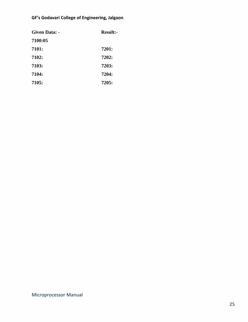
Given Data: - Result:-
7100:05
7101: 7201:
7102: 7202:
7103: 7203:
7104: 7204:
7105: 7205:

GF’s Godavari College of Engineering, Jalgaon.
Microprocessor Manual
26
Oral Questions
Q.1: What is a stack? Why stack is used in a program?
Ans.A stack is a group of memory locations in the R/W memory. The stack is used to store
information temporarily during the execution of a program. Also the stack is used in subroutine calls to
store the return address. As an example, data generated at a certain point in a program may be needed
later in the program. This data is stored in the stack and retrieved when needed. Because the number of
general purpose registers (GPRs) in a microprocessor is limited–hence not all the temporary data can
be stored in them and this is where the stack plays its part.
Q2. How the stack is initialized? Is initialization of stack a must in a program?
Ans.The stack is initialized by a 16-bit register, called the stack pointer (SP) register. No, it is not a
must. If for programs for which any temporary data that are generated can be stored in GPRs and
which don’t require subroutine calls, there is no need to initialize the stack by the SP.
Q3. What the SP register does in a program? Who uses the stack? Comment on the size of the stack.
Ans.The SP register keeps a track with regard to the storage and retrieval of data/information. The
stack is used by both the programmer and the system. Programmer uses the stack for storage/retrieval
of data by using the PUSH/POP instructions respectively.On the other hand, the system uses the stack
to store return address whenever subroutine CALL is used. It depends on the size of the R/W memory,
as well as the program length. Since for agiven system, the size of the R/W memory is fixed, thus
smaller the size of the program, more would be the size of the stack.
Q4.What type of memory is the stack? How the stack is initialized?
Ans. Stack is a ‘last-in first-out’ or LIFO type of memory. This means that data which is pushed last
into stack is popped out of it first. The stack is initialized by means of the stack pointer. The software
instruction is like this: LXI SP, 0044.It means that the stack is initiated at the memory location 4400 by
the stack pointer.

GF’s Godavari College of Engineering, Jalgaon.
Microprocessor Manual
27
Q5.Where, in the R/W memory, a programmer should initialize the stack?
Ans.The stack should be initialized at the high end of the memory map. The user program should start
at the low end of the memory map, while the stack should be initialized at the high end of the memory
map. When the program is being executed, the PC is auto-incremented while as temporary data are
stored in the stack, it is auto-decremented. Thus if sufficient gap is not maintained, the program area
may get corrupted by the filling-in of the stack. In such a case, the program will ‘crash’. This is
explained in following Fig.


