lan8187/lan8187i data sheet -...
TRANSCRIPT

LAN8187/LAN8187i
MII/RMII 10/100 Ethernet Transceiver with HP Auto-MDIX & flexPWR® Technology
Highlights
• Single-Chip Ethernet Physical Layer Transceiver (PHY)
• ESD Protection levels of ±8kV HBM without exter-nal protection devices
• ESD protection levels of EN61000-4-2, ±8kV con-tact mode, and ±15kV for air discharge mode per independent test facility
• Comprehensive flexPWR® Technology
- Flexible Power Management Architecture
• LVCMOS Variable I/O voltage range: +1.6V to +3.6V
• Integrated 3.3V to 1.8V regulator for optional sin-gle supply operation.
- Regulator can be disabled if 1.8V system supply is available.
• Performs HP Auto-MDIX in accordance with IEEE 802.3ab specification
• Automatic Polarity Correction
• Latch-Up Performance Exceeds 150mA per EIA/JESD 78, Class II
• Energy Detect power-down mode
• Low Current consumption power down mode
• Low operating current consumption:
- 39mA typical in 10BASE-T and
- 79mA typical in 100BASE-TX mode
• Supports Auto-negotiation and Parallel Detection
• Supports the Media Independent Interface (MII) and Reduced Media Independent Interface (RMII)
• Compliant with IEEE 802.3-2005 standards
- MII Pins tolerant to 3.6V
• IEEE 802.3-2005 compliant register functions
• Integrated DSP with Adaptive Equalizer
• Baseline Wander (BLW) Correction
• Vendor Specific register functions
• Low profile 64-pin TQFP RoHS compliant pack-age (10 x 10 x 1.4mm)
• 4 LED status indicators
• Commercial Operating Temperature 0 C to 70 C• Industrial Operating Temperature -40 C to 85 C
version available (LAN8187i)
Applications
• Set Top Boxes
• Network Printers and Servers
• LAN on Motherboard
• Embedded Telecom Applications
• Video Record/Playback Systems
• Cable Modems/Routers
• DSL Modems/Routers
• Digital Video Recorders
• Personal Video Recorders
• IP and Video Phones
• Wireless Access Points
• Digital Televisions
• Digital Media Adaptors/Servers
• POS Terminals
• Gaming Consoles
• Security Systems
• Access Control
2009 - 2018 Microchip Technology Inc. DS00002679A-page 1

LAN8187/LAN8187i
TO OUR VALUED CUSTOMERS
It is our intention to provide our valued customers with the best documentation possible to ensure successful use of your Microchipproducts. To this end, we will continue to improve our publications to better suit your needs. Our publications will be refined andenhanced as new volumes and updates are introduced.
If you have any questions or comments regarding this publication, please contact the Marketing Communications Department viaE-mail at [email protected]. We welcome your feedback.
Most Current Data SheetTo obtain the most up-to-date version of this data sheet, please register at our Worldwide Web site at:
http://www.microchip.com
You can determine the version of a data sheet by examining its literature number found on the bottom outside corner of any page. The last character of the literature number is the version number, (e.g., DS30000000A is version A of document DS30000000).
ErrataAn errata sheet, describing minor operational differences from the data sheet and recommended workarounds, may exist for cur-rent devices. As device/documentation issues become known to us, we will publish an errata sheet. The errata will specify therevision of silicon and revision of document to which it applies.
To determine if an errata sheet exists for a particular device, please check with one of the following:• Microchip’s Worldwide Web site; http://www.microchip.com• Your local Microchip sales office (see last page)
When contacting a sales office, please specify which device, revision of silicon and data sheet (include -literature number) you areusing.
Customer Notification SystemRegister on our web site at www.microchip.com to receive the most current information on all of our products.
DS00002679A-page 2 2009 - 2018 Microchip Technology Inc.

2009 - 2018 Microchip Technology Inc. DS00002679A-page 3
LAN8187/LAN8187i
Table of Contents
1.0 General Description ........................................................................................................................................................................ 42.0 Pin Configuration ............................................................................................................................................................................ 63.0 Pin Description ................................................................................................................................................................................ 84.0 Architecture Details ....................................................................................................................................................................... 145.0 Registers ....................................................................................................................................................................................... 296.0 AC Electrical Characteristics ......................................................................................................................................................... 487.0 DC Electrical Characteristics ........................................................................................................................................................ 598.0 Application Notes .......................................................................................................................................................................... 669.0 Package Information ..................................................................................................................................................................... 67Appendix A: Data Sheet Revision History ........................................................................................................................................... 68The Microchip Web Site ...................................................................................................................................................................... 70Customer Change Notification Service ............................................................................................................................................... 70Customer Support ............................................................................................................................................................................... 70Product Identification System ............................................................................................................................................................. 71
LAN8187/LAN8187i
1.0 GENERAL DESCRIPTION
The Microchip LAN8187/LAN8187i is a low-power, industrial temperature (LAN8187i), variable I/O voltage, EthernetTransceiver with HP Auto-MDIX for high-performance embedded Ethernet applications. The LAN8187/LAN8187i canbe configured to operate on a single 3.3V supply utilizing an integrated 3.3V to 1.8V linear regulator. An option is avail-able to disable the linear regulator to optimize system designs that have a 1.8V power plane available.
1.1 Architectural Overview
The LAN8187/LAN8187i consists of an encoder/decoder, scrambler/descrambler, wave-shaping transmitter, outputdriver, twisted-pair receiver with adaptive equalizer and baseline wander (BLW) correction, and clock and data recoveryfunctions. The LAN8187/LAN8187i can be configured to support either the Media Independent Interface (MII) or theReduced Media Independent Interface (RMII).
The LAN8187/LAN8187i is compliant with IEEE 802.3-2005 standards (MII Pins tolerant to 3.6V) and supports bothIEEE 802.3-2005 -compliant and vendor-specific register functions. It contains a full-duplex 10-BASE-T/100BASE-TXtransceiver and supports 10-Mbps (10BASE-T) operation on Category 3 and Category 5 unshielded twisted-pair cable,and 100-Mbps (100BASE-TX) operation on Category 5 unshielded twisted-pair cable.
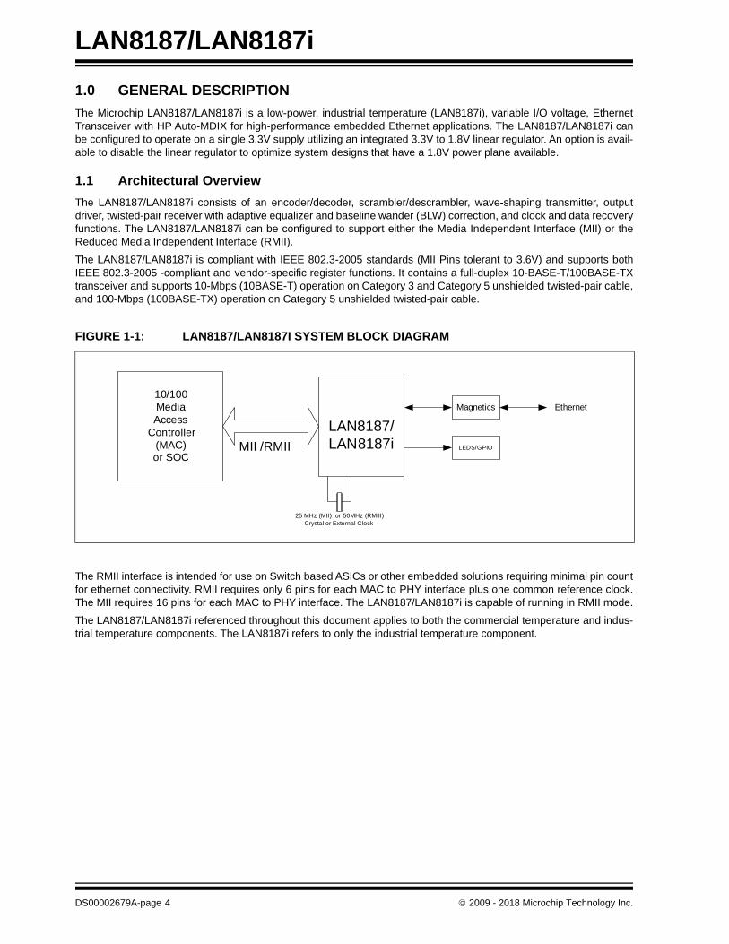
The RMII interface is intended for use on Switch based ASICs or other embedded solutions requiring minimal pin countfor ethernet connectivity. RMII requires only 6 pins for each MAC to PHY interface plus one common reference clock.The MII requires 16 pins for each MAC to PHY interface. The LAN8187/LAN8187i is capable of running in RMII mode.
The LAN8187/LAN8187i referenced throughout this document applies to both the commercial temperature and indus-trial temperature components. The LAN8187i refers to only the industrial temperature component.
FIGURE 1-1: LAN8187/LAN8187I SYSTEM BLOCK DIAGRAM
10/100MediaAccess
Controller(MAC)or SOC
LAN8187/LAN8187i
Magnetics Ethernet
System Bus
LEDS/GPIO
25 MHz (MII) or 50MHz (RMIII)Crystal or External Clock
MII /RMII
DS00002679A-page 4 2009 - 2018 Microchip Technology Inc.

LAN8187/LAN8187i
FIGURE 1-2: LAN8187/LAN8187I ARCHITECTURAL OVERVIEW
10M Rx Logic
100M Rx Logic
DSP System:Clock
Data RecoveryEqualizer
Analog-to-Digital
100M PLL
Squelch & Filters
10M PLL
Receive Section
Central Bias
HP Auto-MDIX
Management ControlSMI
RM
II / MII Lo
gic
TXP / TXN
TXD[0..3]TX_ENTX_ER
TX_CLK
RXD[0..3]RX_DVRX_ER
RX_CLK
CRSCOL/CRS_DV
MDCMDIO
SPEED100LINKACTIVITYFDUPLEX
LED Circuitry
MODE Control
nINT
nRESET RXP / RXN
10M Tx Logic
10M Transmitter
100M Tx Logic
100M Transmitter
Transmit Section
PLLXTAL1
XTAL2
MODE0MODE1MODE2
PHY Address Latches
PHYAD[0..4]
Auto-Negotiation
InterruptGenerator
MII
MDIXControl AMDIX_EN
CH_SELECT
GPO CircuitryGPO0GPO1GPO2
2009 - 2018 Microchip Technology Inc. DS00002679A-page 5

LAN8187/LAN8187i
2.0 PIN CONFIGURATION
2.1 Package Pin Layout Diagram and Signal Table
FIGURE 2-1: PACKAGE PINOUT (TOP VIEW)
GPO1/PHYAD4
GPO0/RMII
GPO2
MODE0
MODE1
MODE2
VSS1
NC
VSS7
COL/CRS_DV
CRS
nINT/TX_ER/TXD4
TXD3
VDDIO
TXD2
TXD1
TXD0
VSS5
NC
EX
RE
S1
AVSS4
AV
SS
3
AV
DD
2
REG
_EN
NC
VSS6
AVDD3
NC
LIN
K/P
HY
AD
1
AC
TIV
ITY
/PH
YA
D2
FD
UP
LE
X/P
HY
AD
3
XTAL2NC
CL
KIN
/XT
AL
1
VSS3
nRST
LAN8187/LAN8187i
1
16
48
33
32
64
49
VSS8
NC
NC
MDIO
MDC
VSS4
TX_EN
TX_CLK
AMDIX_EN
AVDD1
RXP
RXN
VDD33
17
VDD_CORE
VSS2
SPEED100/PHYAD0
RXD
3/nINTSEL
RX
D2
RX
D1
RX
D0
CH_SELECT
RX_ER/RXD4
RX_CLK
RX_DV
AVSS2
AVSS1
TXP
TXN
DS00002679A-page 6 2009 - 2018 Microchip Technology Inc.

LAN8187/LAN8187i
TABLE 2-1: LAN8187/LAN8187I 64-PIN TQFP PINOUT
Pin No. Pin Name Pin No. Pin Name
1 GPO0/RMII 33 RX_DV
2 GPO1/PHYAD4 34 RX_CLK
3 GPO2 35 RX_ER/RXD4
4 MODE0 36 CH_SELECT
5 MODE1 37 AMDIX_EN
6 MODE2 38 TX_CLK
7 VSS1 39 TX_EN
8 NC 40 VSS5
9 VSS7 41 TXD0
10 VSS8 42 TXD1
11 NC 43 VDDIO
12 NC 44 TXD2
13 VDD33 45 TXD3
14 VDD_CORE 46 nINT/TX_ER/TXD4
15 VSS2 47 COL/CRS_DV
16 SPEED100/PHYAD0 48 CRS
17 LINK/PHYAD1 49 AVSS1
18 NC 50 TXN
19 ACTIVITY/PHYAD2 51 TXP
20 FDUPLEX/PHYAD3 52 AVSS2
21 NC 53 AVDD1
22 XTAL2 54 RXN
23 CLKIN/XTAL1 55 RXP
24 VSS3 56 NC
25 nRST 57 AVDD2
26 MDIO 58 AVSS3
27 MDC 59 EXRES1
28 VSS4 60 AVSS4
29 RXD3/nINTSEL 61 AVDD3
30 RXD2 62 VSS6
31 RXD1 63 REG_EN
32 RXD0 64 NC
2009 - 2018 Microchip Technology Inc. DS00002679A-page 7

LAN8187/LAN8187i
3.0 PIN DESCRIPTION
This chapter describes the signals on each pin. When a lower case “n” is used at the beginning of the signal name, itindicates that the signal is active low. For example, nRST indicates that the reset signal is active low.
3.1 I/O Signals
I Input. Digital LVCMOS levels.
O Output. Digital LVCMOS levels.
I/O Input or Output. Digital LVCMOS levels.
AI Input. Analog levels.
AO Output. Analog levels.
Note: The digital signals are not 5V tolerant. They are variable voltage from +1.6V to +3.6V.
TABLE 3-1: MII SIGNALS
Signal Name Type Description
TXD0 I Transmit Data 0: Bit 0 of the 4 data bits that are accepted by the PHY for transmission.
TXD1 I Transmit Data 1: Bit 1 of the 4 data bits that are accepted by the PHY for transmission.
TXD2 I Transmit Data 2: Bit 2 of the 4 data bits that are accepted by the PHY for transmission
Note: This signal should be grounded in RMII Mode.
TXD3 I Transmit Data 3: Bit 3 of the 4 data bits that are accepted by the PHY for transmission.
Note: This signal should be grounded in RMII Mode
nINT/TX_ER/TXD4
I/O MII Transmit Error: When driven high, the 4B/5B encode process substitutes the Transmit Error code-group (/H/) for the encoded data word. This input is ignored in 10Base-T operation.
MII Transmit Data 4: In Symbol Interface (5B Decoding) mode, this signal becomes the MII Transmit Data 4 line, the MSB of the 5-bit symbol code-group.
Note:
• This signal is not used in RMII Mode.
• This signal is mux’d with nINT
• See Section 4.10, "(TX_ER/TXD4)/nINT Strapping," on page 25 for additional information on configuration/strapping options.
TX_EN I Transmit Enable: Indicates that valid data is presented on the TXD[3:0] signals, for transmission. In RMII Mode, only TXD[1:0] have valid data.
TX_CLK O Transmit Clock: 25MHz in 100Base-TX mode. 2.5MHz in 10Base-T mode.
Note: This signal is not used in RMII Mode
RXD0 O Receive Data 0: Bit 0 of the 4 data bits that are sent by the PHY in the receive path.
RXD1 O Receive Data 1: Bit 1 of the 4 data bits that are sent by the PHY in the receive path.
RXD2 O Receive Data 2: Bit 2 of the 4 data bits that sent by the PHY in the receive path.
Note: This signal is not used in RMII Mode.
DS00002679A-page 8 2009 - 2018 Microchip Technology Inc.

LAN8187/LAN8187i
RXD3/nINTSEL
O Receive Data 3: Bit 3 of the 4 data bits that sent by the PHY in the receive path.
nINTSEL: On power-up or external reset, the mode of the nINT/TXER/TXD4 pin is selected. • When floated or pulled to VDDIO, nINT is selected (default).
• When pulled low to VSS through a Pull-down resistor (see Table 4-5, “Boot Strapping Configuration Resistors,” on page 26), TXER/TXD4 is selected.
Note:
• RXD3 is not used in RMII Mode
• If the nINT/TXER/TXD4 pin is configured for nINT mode, it needs a pull-up resistor to VDDIO.
• See Section 4.10, "(TX_ER/TXD4)/nINT Strapping," on page 25 for additional information on configuration/strapping options.
RX_ER/RXD4
I/O Receive Error: Asserted to indicate that an error was detected somewhere in the frame presently being transferred from the PHY.
MII Receive Data 4: In Symbol Interface (5B Decoding) mode, this signal is the MII Receive Data 4 signal, the MSB of the received 5-bit symbol code-group. Unless configured in this mode, the pin functions as RX_ER.
Note: This pin has an internal pull-down resistor, and must notbe high during reset. The RX_ER signal is optional inRMII Mode.
RX_CLK O Receive Clock: 25MHz in 100Base-TX mode. 2.5MHz in 10Base-T mode.
Note: This signal is not used in RMII Mode
COL/CRS_DV O MII Collision Detect: Asserted to indicate detection of collision condition.
RMII CRS_DV (Carrier Sense/Receive Data Valid) Asserted to indicate when the receive medium is non-idle. When a 10BT packet is received, CRS_DV is asserted, but RXD[1:0] is held low until the SFD byte (10101011) is received. In 10BT, half-duplex mode, transmitted data is not looped back onto the receive data pins, per the RMII standard.
Note: See Section 4.6.3, "MII vs. RMII Configuration," onpage 21 for more details.
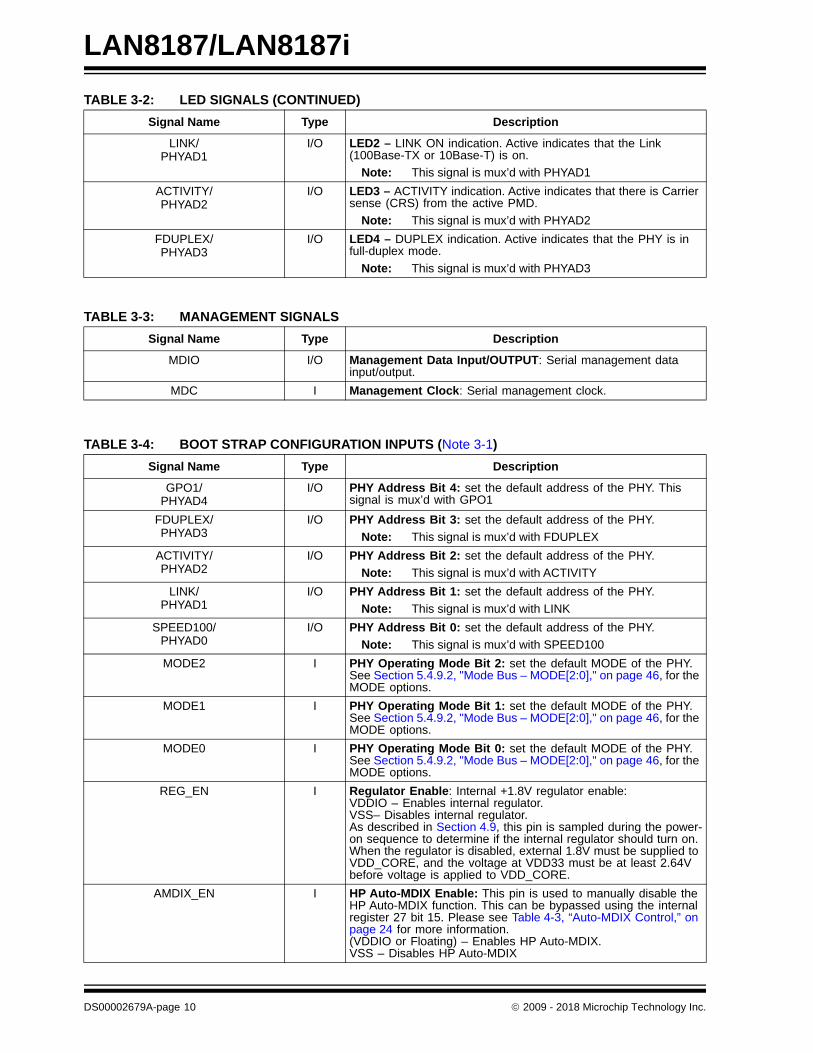
TABLE 3-2: LED SIGNALS
Signal Name Type Description
CRS O Carrier Sense: Indicates detection of carrier.
RX_DV O Receive Data Valid: Indicates that recovered and decoded data nibbles are being presented on RXD[3:0].
Note: This pin has an internal pull-down resistor, and must notbe high during reset. This signal is not used in RMIIMode.
SPEED100/PHYAD0
I/O LED1 – SPEED100 indication. Active indicates that the selected speed is 100Mbps. Inactive indicates that the selected speed is 10Mbps.
Note: This signal is mux’d with PHYAD0
TABLE 3-1: MII SIGNALS (CONTINUED)
Signal Name Type Description
2009 - 2018 Microchip Technology Inc. DS00002679A-page 9
LAN8187/LAN8187i
LINK/PHYAD1
I/O LED2 – LINK ON indication. Active indicates that the Link (100Base-TX or 10Base-T) is on.
Note: This signal is mux’d with PHYAD1
ACTIVITY/PHYAD2
I/O LED3 – ACTIVITY indication. Active indicates that there is Carrier sense (CRS) from the active PMD.
Note: This signal is mux’d with PHYAD2
FDUPLEX/PHYAD3
I/O LED4 – DUPLEX indication. Active indicates that the PHY is in full-duplex mode.
Note: This signal is mux’d with PHYAD3
TABLE 3-3: MANAGEMENT SIGNALS
Signal Name Type Description
MDIO I/O Management Data Input/OUTPUT: Serial management data input/output.
MDC I Management Clock: Serial management clock.
TABLE 3-4: BOOT STRAP CONFIGURATION INPUTS (Note 3-1)
Signal Name Type Description
GPO1/PHYAD4
I/O PHY Address Bit 4: set the default address of the PHY. This signal is mux’d with GPO1
FDUPLEX/PHYAD3
I/O PHY Address Bit 3: set the default address of the PHY.
Note: This signal is mux’d with FDUPLEX
ACTIVITY/PHYAD2
I/O PHY Address Bit 2: set the default address of the PHY.
Note: This signal is mux’d with ACTIVITY
LINK/PHYAD1
I/O PHY Address Bit 1: set the default address of the PHY.
Note: This signal is mux’d with LINK
SPEED100/PHYAD0
I/O PHY Address Bit 0: set the default address of the PHY.
Note: This signal is mux’d with SPEED100
MODE2 I PHY Operating Mode Bit 2: set the default MODE of the PHY. See Section 5.4.9.2, "Mode Bus – MODE[2:0]," on page 46, for the MODE options.
MODE1 I PHY Operating Mode Bit 1: set the default MODE of the PHY. See Section 5.4.9.2, "Mode Bus – MODE[2:0]," on page 46, for the MODE options.
MODE0 I PHY Operating Mode Bit 0: set the default MODE of the PHY. See Section 5.4.9.2, "Mode Bus – MODE[2:0]," on page 46, for the MODE options.
REG_EN I Regulator Enable: Internal +1.8V regulator enable:VDDIO – Enables internal regulator. VSS– Disables internal regulator.As described in Section 4.9, this pin is sampled during the power-on sequence to determine if the internal regulator should turn on. When the regulator is disabled, external 1.8V must be supplied to VDD_CORE, and the voltage at VDD33 must be at least 2.64V before voltage is applied to VDD_CORE.
AMDIX_EN I HP Auto-MDIX Enable: This pin is used to manually disable the HP Auto-MDIX function. This can be bypassed using the internal register 27 bit 15. Please see Table 4-3, “Auto-MDIX Control,” on page 24 for more information.(VDDIO or Floating) – Enables HP Auto-MDIX. VSS – Disables HP Auto-MDIX
TABLE 3-2: LED SIGNALS (CONTINUED)
Signal Name Type Description
DS00002679A-page 10 2009 - 2018 Microchip Technology Inc.

LAN8187/LAN8187i
Note 3-1 On nRST transition high, the PHY latches the state of the configuration pins in this table.
CH_SELECT I Channel Select: This pin is used in conjunction with the AMDIX_EN pin above to manual select the channel to transmit and receive on. For more information please see Table 4-3, “Auto-MDIX Control,” on page 24
(VDDIO or Floating) – MDIX - TX pair receives RX pair transmits.0V – MDI -TX pair transmits RX pair receives.
GPO0/RMII I/O General Purpose Output 0 – General Purpose Output signal. Driven by bits in registers 27 and 31.
RMII – MII/RMII mode selection is latched on the rising edge of the internal reset (nreset) based on the following strapping:
Float the GPO0 pin for MII mode or pull-high with an external Pull-up resistor (see Table 4-5, “Boot Strapping Configuration Resistors,” on page 26) to VDDIO to set the device in RMII mode.
Note: See Section 4.6.3, "MII vs. RMII Configuration," onpage 21 for more details.
TABLE 3-5: GENERAL SIGNALS
Signal Name Type Description
nINT I/O LAN Interrupt – Active Low output. Place a pull-up external resistor (see Table 4-5, “Boot Strapping Configuration Resistors,” on page 26) to VCC 3.3V.
Note:
• This signal is mux’d with TX_ER/TXD4
• See Section 4.10, "(TX_ER/TXD4)/nINT Strapping," on page 25 for additional details on Strapping options.
nRST I External Reset – input of the system reset. This signal is active LOW. When this pin is deasserted, the mode register bits are loaded from the mode pins as described in Section 5.4.9.2.
CLKIN/XTAL1 I Clock Input – 25 Mhz or 50 MHz external clock or crystal input.
In MII mode, this signal is the 25 MHz reference input clock
In RMII mode, this signal is the 50 MHz reference input clock which is typically also driven to the RMII compliant Ethernet MAC clock input.
Note: See Section 4.10, "(TX_ER/TXD4)/nINT Strapping," onpage 25 for additional details on Strapping options.
XTAL2 O Clock Output – 25 MHz crystal output.
Note: See Section 4.10, "(TX_ER/TXD4)/nINT Strapping," onpage 25 for additional details on Strapping options.Also, float this pin if using an external clock being driventhrough CLKIN/XTAL1
GPO2 O General Purpose Output 2 – General Purpose Output signal Driven by bits in registers 27 and 31.
TABLE 3-4: BOOT STRAP CONFIGURATION INPUTS (Note 3-1) (CONTINUED)
Signal Name Type Description
2009 - 2018 Microchip Technology Inc. DS00002679A-page 11

LAN8187/LAN8187i
GPO1 O General Purpose Output 1 – General Purpose Output signal Driven by bits in registers 27 and 31. This signal is mux’d with PHYAD4.
GPO0/RMII I/O General Purpose Output 0 – General Purpose Output signal. Driven by bits in registers 27 and 31.
RMII – MII/RMII mode selection is latched on the rising edge of nRST based on the following strapping:
Float the GPO0 pin for MII mode or pull-high with an external resistor to VDDIO to set the device in RMII mode. See Table 4-5, “Boot Strapping Configuration Resistors,” on page 26.
Note: See Section 4.6.3, "MII vs. RMII Configuration," onpage 21 for more details.
TABLE 3-6: 10/100 LINE INTERFACE
Signal Name Type Description
TXP AO Transmit Data: 100Base-TX or 10Base-T differential transmit outputs to magnetics.
TXN AO Transmit Data: 100Base-TX or 10Base-T differential transmit outputs to magnetics.
RXP AI Receive Data: 100Base-TX or 10Base-T differential receive inputs from magnetics.
RXN AI Receive Data: 100Base-TX or 10Base-T differential receive inputs from magnetics.
TABLE 3-7: ANALOG REFERENCES
Signal Name Type Description
EXRES1 AI Connects to reference resistor of value 12.4K-Ohm, 1% connected as described in the Analog Layout Guidelines. The nominal voltage is 1.2V and therefore the resistor will dissipate approximately 1mW of power.
TABLE 3-8: NO CONNECT SIGNALS
Signal Name Type Description
NC No Connect
TABLE 3-5: GENERAL SIGNALS (CONTINUED)
Signal Name Type Description
DS00002679A-page 12 2009 - 2018 Microchip Technology Inc.

LAN8187/LAN8187i
TABLE 3-9: POWER SIGNALS
Signal Name Type Description
AVDD[1-3] POWER +3.3V Analog Power
AVSS[1-4] POWER Analog Ground
VDD_CORE POWER +1.8V (Core voltage) - 1.8V for digital circuitry on chip. Supplied by the on-chip regulator unless the regulator is disabled by grounding the REG_EN pin. Place a 0.1uF capacitor near this pin and connect the capacitor from this pin to ground. When using the on-chip regulator, place a 4.7uF ±20% capacitor with ESR < 1ohm near this pin and connect the capacitor from this pin to ground. X5R or X7R ceramic capacitors are recommended since they exhibit an ESR lower than 0.1ohm at frequencies greater than 10kHz.
VDD33 POWER +3.3V Digital Power
VDDIO POWER +1.6V to +3.6V Variable I/O Pad Power
VSS[1-8] POWER Digital Ground (GND)
2009 - 2018 Microchip Technology Inc. DS00002679A-page 13

LAN8187/LAN8187i
4.0 ARCHITECTURE DETAILS
4.1 Top Level Functional Architecture
Functionally, the PHY can be divided into the following sections:
• 100Base-TX transmit and receive
• 10Base-T transmit and receive
• MII or RMII interface to the controller
• Auto-negotiation to automatically determine the best speed and duplex possible
• Management Control to read status registers and write control registers
4.2 100Base-TX Transmit
The data path of the 100Base-TX is shown in Figure 4-1. Each major block is explained below.
4.2.1 100M TRANSMIT DATA ACROSS THE MII/RMII
For MII, the MAC controller drives the transmit data onto the TXD bus and asserts TX_EN to indicate valid data. Thedata is latched by the PHY’s MII block on the rising edge of TX_CLK. The data is in the form of 4-bit wide 25MHz data.
The MAC controller drives the transmit data onto the TXD bus and asserts TX_EN to indicate valid data. The data islatched by the PHY’s MII block on the rising edge of REF_CLK. The data is in the form of 2-bit wide 50MHz data.
4.2.2 4B/5B ENCODING
The transmit data passes from the MII block to the 4B/5B encoder. This block encodes the data from 4-bit nibbles to 5-bit symbols (known as “code-groups”) according to Table 4-1. Each 4-bit data-nibble is mapped to 16 of the 32 possiblecode-groups. The remaining 16 code-groups are either used for control information or are not valid.
The first 16 code-groups are referred to by the hexadecimal values of their corresponding data nibbles, 0 through F. Theremaining code-groups are given letter designations with slashes on either side. For example, an IDLE code-group is/I/, a transmit error code-group is /H/, etc.
The encoding process may be bypassed by clearing bit 6 of register 31. When the encoding is bypassed the 5th transmitdata bit is equivalent to TX_ER.
Note that encoding can be bypassed only when the MAC interface is configured to operate in MII mode.
FIGURE 4-1: 100BASE-TX DATA PATH
M AC
TxDriver
M LT-3Converter
N R ZIC onverter
4B /5BEncoder
M agnetics
CAT-5R J45
25M Hz by5 bits
N RZI
M LT-3
M LT-3
M LT-3
M LT -3
Scram blerand P ISO
125 M bps Seria l
M II 25M H zby 4 b its
T X _C LK(for M II only)
Ext R ef_C LK (for R M II only)
100MPLL
M II 25 M hz by 4 b itsor
R M II 50M hz by 2 b its
DS00002679A-page 14 2009 - 2018 Microchip Technology Inc.

LAN8187/LAN8187i
4.2.3 SCRAMBLING
Repeated data patterns (especially the IDLE code-group) can have power spectral densities with large narrow-bandpeaks. Scrambling the data helps eliminate these peaks and spread the signal power more uniformly over the entirechannel bandwidth. This uniform spectral density is required by FCC regulations to prevent excessive EMI from beingradiated by the physical wiring.
TABLE 4-1: 4B/5B CODE TABLE
Code Group SYM Receiver Interpretation Transmitter Interpretation
11110 0 0 0000 DATA 0 0000 DATA
01001 1 1 0001 1 0001
10100 2 2 0010 2 0010
10101 3 3 0011 3 0011
01010 4 4 0100 4 0100
01011 5 5 0101 5 0101
01110 6 6 0110 6 0110
01111 7 7 0111 7 0111
10010 8 8 1000 8 1000
10011 9 9 1001 9 1001
10110 A A 1010 A 1010
10111 B B 1011 B 1011
11010 C C 1100 C 1100
11011 D D 1101 D 1101
11100 E E 1110 E 1110
11101 F F 1111 F 1111
11111 I IDLE Sent after /T/R until TX_EN
11000 J First nibble of SSD, translated to “0101” following IDLE, else RX_ER
Sent for rising TX_EN
10001 K Second nibble of SSD, translated to “0101” following J, else RX_ER
Sent for rising TX_EN
01101 T First nibble of ESD, causes de-assertion of CRS if followed by /R/, else assertion of RX_ER
Sent for falling TX_EN
00111 R Second nibble of ESD, causes deassertion of CRS if following /T/, else assertion of RX_ER
Sent for falling TX_EN
00100 H Transmit Error Symbol Sent for rising TX_ER
00110 V INVALID, RX_ER if during RX_DV INVALID
11001 V INVALID, RX_ER if during RX_DV INVALID
00000 V INVALID, RX_ER if during RX_DV INVALID
00001 V INVALID, RX_ER if during RX_DV INVALID
00010 V INVALID, RX_ER if during RX_DV INVALID
00011 V INVALID, RX_ER if during RX_DV INVALID
00101 V INVALID, RX_ER if during RX_DV INVALID
01000 V INVALID, RX_ER if during RX_DV INVALID
01100 V INVALID, RX_ER if during RX_DV INVALID
10000 V INVALID, RX_ER if during RX_DV INVALID
2009 - 2018 Microchip Technology Inc. DS00002679A-page 15

LAN8187/LAN8187i
The seed for the scrambler is generated from the PHY address, PHYAD[4:0], ensuring that in multiple-PHY applications,such as repeaters or switches, each PHY will have its own scrambler sequence.
The scrambler also performs the Parallel In Serial Out conversion (PISO) of the data.
4.2.4 NRZI AND MLT3 ENCODING
The scrambler block passes the 5-bit wide parallel data to the NRZI converter where it becomes a serial 125MHz NRZIdata stream. The NRZI is encoded to MLT-3. MLT3 is a tri-level code where a change in the logic level represents a codebit “1” and the logic output remaining at the same level represents a code bit “0”.
4.2.5 100M TRANSMIT DRIVER
The MLT3 data is then passed to the analog transmitter, which drives the differential MLT-3 signal, on outputs TXP andTXN, to the twisted pair media across a 1:1 ratio isolation transformer. The 10Base-T and 100Base-TX signals passthrough the same transformer so that common “magnetics” can be used for both. The transmitter drives into the 100impedance of the CAT-5 cable. Cable termination and impedance matching require external components.
4.2.6 100M PHASE LOCK LOOP (PLL)
The 100M PLL locks onto reference clock and generates the 125MHz clock used to drive the 125 MHz logic and the100Base-Tx Transmitter.
FIGURE 4-2: RECEIVE DATA PATH
MAC
A/D Converter
MLT-3 Converter
NRZI Converter
4B/5B Decoder
Magnetics CAT-5RJ45
100M PLL
MII 25Mhz by 4 bitsor
RMII 50Mhz by 2 bits
RX_CLK(for MII only)
25MHz by5 bits
NRZI
MLT-3MLT-3 MLT-3
6 bit Data
Descrambler and SIPO
125 Mbps Serial
DSP: Timing recovery, Equalizer and BLW Correction
MLT-3
MII/RMII 25MHzby 4 bits
Ext Ref_CLK (for RMII only)
DS00002679A-page 16 2009 - 2018 Microchip Technology Inc.
LAN8187/LAN8187i
4.3 100Base-TX Receive
The receive data path is shown in Figure 4-2. Detailed descriptions are given below.
4.3.1 100M RECEIVE INPUT
The MLT-3 from the cable is fed into the PHY (on inputs RXP and RXN) via a 1:1 ratio transformer. The ADC samplesthe incoming differential signal at a rate of 125M samples per second. Using a 64-level quanitizer it generates 6 digitalbits to represent each sample. The DSP adjusts the gain of the ADC according to the observed signal levels such thatthe full dynamic range of the ADC can be used.
4.3.2 EQUALIZER, BASELINE WANDER CORRECTION AND CLOCK AND DATA RECOVERY
The 6 bits from the ADC are fed into the DSP block. The equalizer in the DSP section compensates for phase and ampli-tude distortion caused by the physical channel consisting of magnetics, connectors, and CAT- 5 cable. The equalizercan restore the signal for any good-quality CAT-5 cable between 1m and 150m.
If the DC content of the signal is such that the low-frequency components fall below the low frequency pole of the iso-lation transformer, then the droop characteristics of the transformer will become significant and Baseline Wander (BLW)on the received signal will result. To prevent corruption of the received data, the PHY corrects for BLW and can receivethe ANSI X3.263-1995 FDDI TP-PMD defined “killer packet” with no bit errors.
The 100M PLL generates multiple phases of the 125MHz clock. A multiplexer, controlled by the timing unit of the DSP,selects the optimum phase for sampling the data. This is used as the received recovered clock. This clock is used toextract the serial data from the received signal.
4.3.3 NRZI AND MLT-3 DECODING
The DSP generates the MLT-3 recovered levels that are fed to the MLT-3 converter. The MLT-3 is then converted to anNRZI data stream.
4.3.4 DESCRAMBLING
The descrambler performs an inverse function to the scrambler in the transmitter and also performs the Serial In ParallelOut (SIPO) conversion of the data.
During reception of IDLE (/I/) symbols. the descrambler synchronizes its descrambler key to the incoming stream. Oncesynchronization is achieved, the descrambler locks on this key and is able to descramble incoming data.
Special logic in the descrambler ensures synchronization with the remote PHY by searching for IDLE symbols within awindow of 4000 bytes (40us). This window ensures that a maximum packet size of 1514 bytes, allowed by the IEEE802.3 standard, can be received with no interference. If no IDLE-symbols are detected within this time-period, receiveoperation is aborted and the descrambler re-starts the synchronization process.
The descrambler can be bypassed by setting bit 0 of register 31.
4.3.5 ALIGNMENT
The de-scrambled signal is then aligned into 5-bit code-groups by recognizing the /J/K/ Start-of-Stream Delimiter (SSD)pair at the start of a packet. Once the code-word alignment is determined, it is stored and utilized until the next start offrame.
4.3.6 5B/4B DECODING
The 5-bit code-groups are translated into 4-bit data nibbles according to the 4B/5B table. The translated data is pre-sented on the RXD[3:0] signal lines. The SSD, /J/K/, is translated to “0101 0101” as the first 2 nibbles of the MAC pre-amble. Reception of the SSD causes the PHY to assert the RX_DV signal, indicating that valid data is available on theRXD bus. Successive valid code-groups are translated to data nibbles. Reception of either the End of Stream Delimiter(ESD) consisting of the /T/R/ symbols, or at least two /I/ symbols causes the PHY to de-assert carrier sense and RX_DV.
These symbols are not translated into data.
The decoding process may be bypassed by clearing bit 6 of register 31. When the decoding is bypassed the 5th receivedata bit is driven out on RX_ER/RXD4. Decoding may be bypassed only when the MAC interface is in MII mode.
2009 - 2018 Microchip Technology Inc. DS00002679A-page 17

LAN8187/LAN8187i
4.3.7 RECEIVE DATA VALID SIGNAL
The Receive Data Valid signal (RX_DV) indicates that recovered and decoded nibbles are being presented on theRXD[3:0] outputs synchronous to RX_CLK. RX_DV becomes active after the /J/K/ delimiter has been recognized andRXD is aligned to nibble boundaries. It remains active until either the /T/R/ delimiter is recognized or link test indicatesfailure or SIGDET becomes false.
RX_DV is asserted when the first nibble of translated /J/K/ is ready for transfer over the Media Independent Interface(MII).
4.3.8 RECEIVER ERRORS
During a frame, unexpected code-groups are considered receive errors. Expected code groups are the DATA set (0through F), and the /T/R/ (ESD) symbol pair. When a receive error occurs, the RX_ER signal is asserted and arbitrarydata is driven onto the RXD[3:0] lines. Should an error be detected during the time that the /J/K/ delimiter is beingdecoded (bad SSD error), RX_ER is asserted true and the value ‘1110’ is driven onto the RXD[3:0] lines. Note that theValid Data signal is not yet asserted when the bad SSD error occurs.
4.3.9 100M RECEIVE DATA ACROSS THE MII/RMII INTERFACE
In MII mode, the 4-bit data nibbles are sent to the MII block. These data nibbles are clocked to the controller at a rateof 25MHz. The controller samples the data on the rising edge of RX_CLK. To ensure that the setup and hold require-ments are met, the nibbles are clocked out of the PHY on the falling edge of RX_CLK. RX_CLK is the 25MHz outputclock for the MII bus. It is recovered from the received data to clock the RXD bus. If there is no received signal, it isderived from the system reference clock (CLKIN).
When tracking the received data, RX_CLK has a maximum jitter of 0.8ns (provided that the jitter of the input clock,CLKIN, is below 100ps).
In RMII mode, the 2-bit data nibbles are sent to the RMII block. These data nibbles are clocked to the controller at a rateof 50MHz. The controller samples the data on the rising edge of CLKIN/XTAL1 (REF_CLK). To ensure that the setupand hold requirements are met, the nibbles are clocked out of the PHY on the falling edge of CLKIN/XTAL1 (REF_CLK).
4.4 10Base-T Transmit
Data to be transmitted comes from the MAC layer controller. The 10Base-T transmitter receives 4-bit nibbles from theMII at a rate of 2.5MHz and converts them to a 10Mbps serial data stream. The data stream is then Manchester-encodedand sent to the analog transmitter, which drives a signal onto the twisted pair via the external magnetics.
The 10M transmitter uses the following blocks:
• MII (digital)
• TX 10M (digital)
• 10M Transmitter (analog)
• 10M PLL (analog)
4.4.1 10M TRANSMIT DATA ACROSS THE MII/RMII INTERFACE
The MAC controller drives the transmit data onto the TXD BUS. For MII, when the controller has driven TX_EN high toindicate valid data, the data is latched by the MII block on the rising edge of TX_CLK. The data is in the form of 4-bitwide 2.5MHz data.
FIGURE 4-3: RELATIONSHIP BETWEEN RECEIVED DATA AND SPECIFIC MII SIGNALS
5 D5 data data data dataRXD
RX_DV
RX_CLK
5 D5 data data data dataCLEAR-TEXT 5J K
5 5 5
T R Idle
DS00002679A-page 18 2009 - 2018 Microchip Technology Inc.

LAN8187/LAN8187i
In order to comply with legacy 10Base-T MAC/Controllers, in Half-duplex mode the PHY loops back the transmitteddata, on the receive path. This does not confuse the MAC/Controller since the COL signal is not asserted during thistime. The PHY also supports the SQE (Heartbeat) signal. See Section 5.4.2, "Collision Detect," on page 43, for moredetails.
For RMII, TXD[1:0] shall transition synchronously with respect to REF_CLK. When TX_EN is asserted, TXD[1:0] areaccepted for transmission by the LAN8187/LAN8187i. TXD[1:0] shall be “00” to indicate idle when TX_EN is deasserted.Values of TXD[1:0] other than “00” when TX_EN is deasserted are reserved for out-of-band signaling (to be defined).Values other than “00” on TXD[1:0] while TX_EN is deasserted shall be ignored by the LAN8187/LAN8187i.TXD[1:0]shall provide valid data for each REF_CLK period while TX_EN is asserted.
4.4.2 MANCHESTER ENCODING
The 4-bit wide data is sent to the TX10M block. The nibbles are converted to a 10Mbps serial NRZI data stream. The10M PLL locks onto the external clock or internal oscillator and produces a 20MHz clock. This is used to Manchesterencode the NRZ data stream. When no data is being transmitted (TX_EN is low), the TX10M block outputs Normal LinkPulses (NLPs) to maintain communications with the remote link partner.
4.4.3 10M TRANSMIT DRIVERS
The Manchester encoded data is sent to the analog transmitter where it is shaped and filtered before being driven outas a differential signal across the TXP and TXN outputs.
4.5 10Base-T Receive
The 10Base-T receiver gets the Manchester- encoded analog signal from the cable via the magnetics. It recovers thereceive clock from the signal and uses this clock to recover the NRZI data stream. This 10M serial data is converted to4-bit data nibbles which are passed to the controller across the MII at a rate of 2.5MHz.
This 10M receiver uses the following blocks:
• Filter and SQUELCH (analog)
• 10M PLL (analog)
• RX 10M (digital)
• MII (digital)
4.5.1 10M RECEIVE INPUT AND SQUELCH
The Manchester signal from the cable is fed into the PHY (on inputs RXP and RXN) via 1:1 ratio magnetics. It is firstfiltered to reduce any out-of-band noise. It then passes through a SQUELCH circuit. The SQUELCH is a set of amplitudeand timing comparators that normally reject differential voltage levels below 300mV and detect and recognize differentialvoltages above 585mV.
4.5.2 MANCHESTER DECODING
The output of the SQUELCH goes to the RX10M block where it is validated as Manchester encoded data. The polarityof the signal is also checked. If the polarity is reversed (local RXP is connected to RXN of the remote partner and viceversa), then this is identified and corrected. The reversed condition is indicated by the flag “XPOL“, bit 4 in register 27.The 10M PLL is locked onto the received Manchester signal and from this, generates the received 20MHz clock. Usingthis clock, the Manchester encoded data is extracted and converted to a 10MHz NRZI data stream. It is then convertedfrom serial to 4-bit wide parallel data.
The RX10M block also detects valid 10Base-T IDLE signals - Normal Link Pulses (NLPs) - to maintain the link.
4.5.3 10M RECEIVE DATA ACROSS THE MII/RMII INTERFACE
For MII, the 4 bit data nibbles are sent to the MII block. In MII mode, these data nibbles are valid on the rising edge ofthe 2.5 MHz RX_CLK.
For RMII, the 2bit data nibbles are sent to the RMII block. In RMII mode, these data nibbles are valid on the rising edgeof the RMII REF_CLK.
2009 - 2018 Microchip Technology Inc. DS00002679A-page 19
LAN8187/LAN8187i
4.5.4 JABBER DETECTION
Jabber is a condition in which a station transmits for a period of time longer than the maximum permissible packet length,usually due to a fault condition, that results in holding the TX_EN input for a long period. Special logic is used to detectthe jabber state and abort the transmission to the line, within 45ms. Once TX_EN is deasserted, the logic resets thejabber condition.
As shown in Figure 5-31, bit 1.1 indicates that a jabber condition was detected.
4.6 MAC Interface
The MII/RMII block is responsible for the communication with the controller. Special sets of hand-shake signals are usedto indicate that valid received/transmitted data is present on the 4 bit receive/transmit bus.
The device must be configured in MII or RMII mode. This is done by specific pin strapping configurations.
See section Section 4.6.3, "MII vs. RMII Configuration," on page 21 for information on pin strapping and how the pinsare mapped differently.
4.6.1 MII
The MII includes 16 interface signals:
• transmit data - TXD[3:0]
• transmit strobe - TX_EN
• transmit clock - TX_CLK
• transmit error - TX_ER/TXD4
• receive data - RXD[3:0]
• receive strobe - RX_DV
• receive clock - RX_CLK
• receive error - RX_ER/RXD4
• collision indication - COL
• carrier sense - CRS
In MII mode, on the transmit path, the PHY drives the transmit clock, TX_CLK, to the controller. The controller synchro-nizes the transmit data to the rising edge of TX_CLK. The controller drives TX_EN high to indicate valid transmit data.The controller drives TX_ER high when a transmit error is detected.
On the receive path, the PHY drives both the receive data, RXD[3:0], and the RX_CLK signal. The controller clocks inthe receive data on the rising edge of RX_CLK when the PHY drives RX_DV high. The PHY drives RX_ER high whena receive error is detected.
4.6.2 RMII
The Microchip LAN8187/LAN8187i supports the low pin count Reduced Media Independent Interface (RMII) intendedfor use between Ethernet PHYs and Switch ASICs. Under IEEE 802.3, an MII comprised of 16 pins for data and controlis defined. In devices incorporating many MACs or PHY interfaces such as switches, the number of pins can add sig-nificant cost as the port counts increase. The management interface (MDIO/MDC) is identical to MII. The RMII interfacehas the following characteristics:
• It is capable of supporting 10Mb/s and 100Mb/s data rates
• A single clock reference is sourced from the MAC to PHY (or from an external source)
• It provides independent 2 bit wide (di-bit) transmit and receive data paths
• It uses LVCMOS signal levels, compatible with common digital CMOS ASIC processes
The RMII includes 6 interface signals with one of the signals being optional:
• transmit data - TXD[1:0]
• transmit strobe - TX_EN
• receive data - RXD[1:0]
• receive error - RX_ER (Optional)
• carrier sense - CRS_DV
• Reference Clock - CLKIN/XTAL1 (RMII references usually define this signal as REF_CLK)
DS00002679A-page 20 2009 - 2018 Microchip Technology Inc.

LAN8187/LAN8187i
4.6.2.1 Reference Clock
The Reference Clock - CLKIN, is a continuous clock that provides the timing reference for CRS_DV, RXD[1:0], TX_EN,TXD[1:0], and RX_ER. The Reference Clock is sourced by the MAC or an external source. Switch implementations maychoose to provide REF_CLK as an input or an output depending on whether they provide a REF_CLK output or rely onan external clock distribution device.
The “Reference Clock” frequency must be 50 MHz +/- 50 ppm with a duty cycle between 40% and 60% inclusive. TheLAN8187/LAN8187i uses the “Reference Clock” as the network clock such that no buffering is required on the transmitdata path. The LAN8187/LAN8187i will recover the clock from the incoming data stream, the receiver will account fordifferences between the local REF_CLK and the recovered clock through use of sufficient elasticity buffering. The elas-ticity buffer does not affect the Inter-Packet Gap (IPG) for received IPGs of 36 bits or greater. To tolerate the clock vari-ations specified here for Ethernet MTUs, the elasticity buffer shall tolerate a minimum of +/-10 bits.
4.6.2.2 CRS_DV - Carrier Sense/Receive Data Valid
The CRS_DV is asserted by the LAN8187/LAN8187i when the receive medium is non-idle. CRS_DV is asserted asyn-chronously on detection of carrier due to the criteria relevant to the operating mode. That is, in 10BASE-T mode, whensquelch is passed or in 100BASE-X mode when 2 non-contiguous zeroes in 10 bits are detected, carrier is said to bedetected.
Loss of carrier shall result in the deassertion of CRS_DV synchronous to the cycle of REF_CLK which presents the firstdi-bit of a nibble onto RXD[1:0] (i.e. CRS_DV is deasserted only on nibble boundaries). If the LAN8187/LAN8187i hasadditional bits to be presented on RXD[1:0] following the initial deassertion of CRS_DV, then the LAN8187/LAN8187ishall assert CRS_DV on cycles of REF_CLK which present the second di-bit of each nibble and de-assert CRS_DV oncycles of REF_CLK which present the first di-bit of a nibble. The result is: Starting on nibble boundaries CRS_DV togglesat 25 MHz in 100Mb/s mode and 2.5 MHz in 10Mb/s mode when CRS ends before RX_DV (i.e. the FIFO still has bitsto transfer when the carrier event ends.) Therefore, the MAC can accurately recover RX_DV and CRS.
During a false carrier event, CRS_DV shall remain asserted for the duration of carrier activity. The data on RXD[1:0] isconsidered valid once CRS_DV is asserted. However, since the assertion of CRS_DV is asynchronous relative toREF_CLK, the data on RXD[1:0] shall be “00” until proper receive signal decoding takes place.
4.6.3 MII VS. RMII CONFIGURATION
The LAN8187/LAN8187i must be configured to support the MII or RMII bus for connectivity to the MAC. This configu-ration is done through the GPO0/RMII pin. To select MII mode, float the GPO0/RMII pin. To select RMII mode, pull-highwith an external resistor (see Table 4-5, “Boot Strapping Configuration Resistors,” on page 26) to VDD33. On the risingedge of the internal reset (nreset), the register bit 18.14 (MIIMODE) is loaded based on the strapping of the GPO0/RMIIpin.
Most of the MII and RMII pins are multiplexed. Table 4-2, "MII/RMII Signal Mapping", shown below, describes the rela-tionship of the related device pins to what pins are used in MII and RMII mode.
TABLE 4-2: MII/RMII SIGNAL MAPPING
Signal Name MII Mode RMII Mode
TXD0 TXD0 TXD0
TXD1 TXD1 TXD1
TX_EN TX_EN TX_EN
RX_ER/RXD4
RX_ER/RXD4/
RX_ERNote 4-2
COL/CRS_DV COL CRS_DV
RXD0 RXD0 RXD0
RXD1 RXD1 RXD1
TXD2 TXD2 Note 4-1
TXD3 TXD3 Note 4-1
TX_ER/TXD4
TX_ER/TXD4
CRS CRS
RX_DV RX_DV
2009 - 2018 Microchip Technology Inc. DS00002679A-page 21

LAN8187/LAN8187i
Note 4-1 In RMII mode, this pin needs to tied to VSS.
Note 4-2 The RX_ER signal is optional on the RMII bus. This signal is required by the PHY, but it is optionalfor the MAC. The MAC can choose to ignore or not use this signal.
4.7 Auto-negotiation
The purpose of the Auto-negotiation function is to automatically configure the PHY to the optimum link parametersbased on the capabilities of its link partner. Auto-negotiation is a mechanism for exchanging configuration informationbetween two link-partners and automatically selecting the highest performance mode of operation supported by bothsides. Auto-negotiation is fully defined in clause 28 of the IEEE 802.3 specification.
Once auto-negotiation has completed, information about the resolved link can be passed back to the controller via theSerial Management Interface (SMI). The results of the negotiation process are reflected in the Speed Indication bits inregister 31, as well as the Link Partner Ability Register (Register 5).
The auto-negotiation protocol is a purely physical layer activity and proceeds independently of the MAC controller.
The advertised capabilities of the PHY are stored in register 4 of the SMI registers. The default advertised by the PHYis determined by user-defined on-chip signal options.
The following blocks are activated during an Auto-negotiation session:
• Auto-negotiation (digital)
• 100M ADC (analog)
• 100M PLL (analog)
• 100M equalizer/BLW/clock recovery (DSP)
• 10M SQUELCH (analog)
• 10M PLL (analog)
• 10M Transmitter (analog)
When enabled, auto-negotiation is started by the occurrence of one of the following events:
• Hardware reset
• Software reset
• Power-down reset
• Link status down
• Setting register 0, bit 9 high (auto-negotiation restart)
On detection of one of these events, the PHY begins auto-negotiation by transmitting bursts of Fast Link Pulses (FLP).These are bursts of link pulses from the 10M transmitter. They are shaped as Normal Link Pulses and can pass uncor-rupted down CAT-3 or CAT-5 cable. A Fast Link Pulse Burst consists of up to 33 pulses. The 17 odd-numbered pulses,which are always present, frame the FLP burst. The 16 even-numbered pulses, which may be present or absent, containthe data word being transmitted. Presence of a data pulse represents a “1”, while absence represents a “0”.
The data transmitted by an FLP burst is known as a “Link Code Word.” These are defined fully in IEEE 802.3 clause 28.In summary, the PHY advertises 802.3 compliance in its selector field (the first 5 bits of the Link Code Word). It adver-tises its technology ability according to the bits set in register 4 of the SMI registers.
There are 4 possible matches of the technology abilities. In the order of priority these are:
• 100M Full Duplex (Highest priority)
• 100M Half Duplex
• 10M Full Duplex
• 10M Half Duplex
RXD2 RXD2
RXD3 RXD3
TX_CLK TX_CLK
RX_CLK RX_CLK
CLKIN/XTAL1 CLKIN/XTAL1 REF_CLK
TABLE 4-2: MII/RMII SIGNAL MAPPING (CONTINUED)
Signal Name MII Mode RMII Mode
DS00002679A-page 22 2009 - 2018 Microchip Technology Inc.

LAN8187/LAN8187i
If the full capabilities of the PHY are advertised (100M, Full Duplex), and if the link partner is capable of 10M and 100M,then auto-negotiation selects 100M as the highest performance mode. If the link partner is capable of Half and Fullduplex modes, then auto-negotiation selects Full Duplex as the highest performance operation.
Once a capability match has been determined, the link code words are repeated with the acknowledge bit set. Any dif-ference in the main content of the link code words at this time will cause auto-negotiation to re-start. Auto-negotiationwill also re-start if not all of the required FLP bursts are received.
The capabilities advertised during auto-negotiation by the PHY are initially determined by the logic levels latched on theMODE[2:0] bus after reset completes. This bus can also be used to disable auto-negotiation on power-up.
Writing register 4 bits [8:5] allows software control of the capabilities advertised by the PHY. Writing register 4 does notautomatically re-start auto-negotiation. Register 0, bit 9 must be set before the new abilities will be advertised. Auto-negotiation can also be disabled via software by clearing register 0, bit 12.
The LAN8187/LAN8187i does not support “Next Page” capability.
4.7.1 PARALLEL DETECTION
If the LAN8187/LAN8187i is connected to a device lacking the ability to auto-negotiate (i.e. no FLPs are detected), it isable to determine the speed of the link based on either 100M MLT-3 symbols or 10M Normal Link Pulses. In this casethe link is presumed to be Half Duplex per the IEEE standard. This ability is known as “Parallel Detection.” This featureensures interoperability with legacy link partners. If a link is formed via parallel detection, then bit 0 in register 6 is clearedto indicate that the Link Partner is not capable of auto-negotiation. The controller has access to this information via themanagement interface. If a fault occurs during parallel detection, bit 4 of register 6 is set.
Register 5 is used to store the Link Partner Ability information, which is coded in the received FLPs. If the Link Partneris not auto-negotiation capable, then register 5 is updated after completion of parallel detection to reflect the speed capa-bility of the Link Partner.
4.7.2 RE-STARTING AUTO-NEGOTIATION
Auto-negotiation can be re-started at any time by setting register 0, bit 9. Auto-negotiation will also re-start if the link isbroken at any time. A broken link is caused by signal loss. This may occur because of a cable break, or because of aninterruption in the signal transmitted by the Link Partner. Auto-negotiation resumes in an attempt to determine the newlink configuration.
If the management entity re-starts Auto-negotiation by writing to bit 9 of the control register, the LAN8187/LAN8187i willrespond by stopping all transmission/receiving operations. Once the break_link_timer is done, in the Auto-negotiationstate-machine (approximately 1200ms) the auto-negotiation will re-start. The Link Partner will have also dropped thelink due to lack of a received signal, so it too will resume auto-negotiation.
4.7.3 DISABLING AUTO-NEGOTIATION
Auto-negotiation can be disabled by setting register 0, bit 12 to zero. The device will then force its speed of operationto reflect the information in register 0, bit 13 (speed) and register 0, bit 8 (duplex). The speed and duplex bits in register0 should be ignored when auto-negotiation is enabled.
4.7.4 HALF VS. FULL DUPLEX
Half Duplex operation relies on the CSMA/CD (Carrier Sense Multiple Access / Collision Detect) protocol to handle net-work traffic and collisions. In this mode, the carrier sense signal, CRS, responds to both transmit and receive activity.In this mode, If data is received while the PHY is transmitting, a collision results.
In Full Duplex mode, the PHY is able to transmit and receive data simultaneously. In this mode, CRS responds only toreceive activity. The CSMA/CD protocol does not apply and collision detection is disabled.
4.8 HP Auto-MDIX
HP Auto-MDIX facilitates the use of CAT-3 (10 Base-T) or CAT-5 (100 Base-T) media UTP interconnect cable withoutconsideration of interface wiring scheme. If a user plugs in either a direct connect LAN cable, or a cross-over patchcable, as shown in TABLE 4-4: on page 25, the Microchip LAN8187/LAN8187i Auto-MDIX PHY is capable of configuringthe TXP/TXN and RXP/RXN pins for correct transceiver operation.
The internal logic of the device detects the TX and RX pins of the connecting device. Since the RX and TX line pairsare interchangeable, special PCB design considerations are needed to accommodate the symmetrical magnetics andtermination of an Auto-MDIX design.
2009 - 2018 Microchip Technology Inc. DS00002679A-page 23

LAN8187/LAN8187i
The Auto-MDIX function can be disabled through an internal register 27, or the external control pins AMDIX_EN. Whendisabled the TX and RX pins can be configured with the Channel Select (CH_SELECT) pin as desired. The table belowshows how the control pins and the register are used to configure the Auto-MDIX function.
TABLE 4-3: AUTO-MDIX CONTROL
Register 27 Bits External Pins Status
15 14 13 AMDIXEN CH_SELECT TX and RX Output Pins
0 X X 1 X Auto-MDIX
0 X X 0 0 Normal MDI
0 X X 0 1 Crossed MDIX
1 1 X X X Auto-MDIX
1 0 0 X X Normal MDI
1 0 1 X X Crossed MDIX
Note:
• X = either 1 or 0.
• X = Don’t Care.
DS00002679A-page 24 2009 - 2018 Microchip Technology Inc.

LAN8187/LAN8187i
4.9 Internal +1.8V Regulator Disable
One feature of the flexPWR technology is the ability to configure the internal 1.8V regulator off. When the regulator isdisabled, external 1.8V must be supplied to VDD_CORE. This makes it possible to reduce total system power, since anexternal switching regulator with greater efficiency than the internal linear regulator may be used to provide the +1.8Vto the PHY circuitry.
4.9.1 DISABLE THE INTERNAL +1.8V REGULATOR
To disable the +1.8V internal regulator, a pulldown strapping resistor (see Table 4-5, “Boot Strapping ConfigurationResistors,” on page 26) is attached from REG_EN to VSS. When both VDDIO and VDDA are within specification, thePHY will sample the REG_EN pin to determine if the internal regulator should turn on. If the pin is grounded to VSS,then the internal regulator is disabled, and the system must supply +1.8V to the VDD_CORE pin. The voltage at VDD33must be at least 2.64V (0.8 * 3.3V) before voltage is applied to VDD_CORE. As described in Section 4.9.2, when theREG_EN pin is left floating or pulled up to VDDIO, then the internal regulator is enabled and the system does not supply+1.8V to the VDD_CORE pin.
When the +1.8V internal regulator is disabled, a 0.1uF capacitor must be added at the VDD_CORE pin and placed closeto the PHY. This capacitance provides decoupling of the external power supply noise.
4.9.2 ENABLE THE INTERNAL +1.8V REGULATOR
To enable the internal regulator, a pull-up resistor (see Table 4-5, “Boot Strapping Configuration Resistors,” on page 26)to VDDIO may be added to the REG_EN pin. When the REG_EN pin is left floating, the internal regulator will also beenabled.
Both a 4.7uF low-ESR and a 0.1uF capacitor must be added at the VDD_CORE pin and placed close to the PHY. Thiscapacitance ensures stability of the internal regulator.
4.10 (TX_ER/TXD4)/nINT Strapping
The TX_ER, TXD4 and nINT functions share a common pin. There are two functional modes for this pin, theTX_ER/TXD4 mode and nINT (interrupt) mode. The RXD3 pin is used to select one of these two functional modes.
The RXD3 pin is latched on the rising edge of the internal reset (nreset) to select the mode. The system designer mustfloat the RXD3 pin for nINT mode or pull-low with an external resistor (see Table 4-5, “Boot Strapping ConfigurationResistors,” on page 26) to VSS to set the device in TX_ER/TXD4 mode. The default setting is high (nINT mode).
TABLE 4-4: DIRECT CABLE CONNECTION VS. CROSS-OVER CABLE CONNECTION.
2009 - 2018 Microchip Technology Inc. DS00002679A-page 25

LAN8187/LAN8187i
4.11 PHY Address Strapping and LED Output Polarity Selection
The PHY ADDRESS bits are latched on the rising edge of the internal reset (nreset). The 5-bit address word[0:4] is inputon the LED1, LED2, LED3, LED4, GPO1 output pins. The default setting is all high 5'b1_1111.
The address lines are strapped as defined in the diagram below. The LED outputs will automatically change polaritybased on the presence of an external pull-down resistor. If the LED pin is pulled high (by an internal 100K pull-up resis-tor) to select a logical high PHY address, then the LED output will be active low. If the LED pin is pulled low (by an exter-nal pull-down resistor (see Table 4-5, “Boot Strapping Configuration Resistors,” on page 26) to select a logical low PHYaddress, the LED output will then be an active high output.
To set the PHY address on the LED pins without LEDs or on the GPO1 or CRS pin, float the pin to set the address highor pull-down the pin with an external resistor (see Table 4-5, “Boot Strapping Configuration Resistors,” on page 26) toGND to set the address low. See the figure below:
4.12 Variable Voltage I/O
The Digital I/O pins on the LAN8187/LAN8187i are variable voltage to take advantage of low power savings from shrink-ing technologies. These pins can operate from a low I/O voltage of +1.6V up to +3.6V. Due to this low voltage featureaddition, the system designer needs to take consideration as for two aspects of their design. Boot strapping configura-tion and I/O voltage stability.
4.12.1 BOOT STRAPPING CONFIGURATION
Due to a lower I/O voltage, a lower strapping resistor needs to be used to ensure the strapped configuration is latchedinto the PHY device at power-on reset.
4.12.2 I/O VOLTAGE STABILITY
The I/O voltage the System Designer applies on VDDIO needs to maintain its value with a tolerance of +/- 10%. Varyingthe voltage up or down, after the PHY has completed power-on reset can cause errors in the PHY operation.
FIGURE 4-4: PHY Address Strapping on LEDs
TABLE 4-5: BOOT STRAPPING CONFIGURATION RESISTORS
I/O Voltage Pull-up/Pull-down Resistor
3.0 to 3.6 10k ohm resistor
2.0 to 3.0 7.5k ohm resistor
1.6 to 2.0 5k ohm resistor
LED1-LED4
~270 ohms
Phy Address = 0LED output = active high
~10K ohms
~270 ohms
LED1-LED4
VDDIO
Phy Address = 1LED output = active low
DS00002679A-page 26 2009 - 2018 Microchip Technology Inc.

LAN8187/LAN8187i
4.13 PHY Management Control
The Management Control module includes 3 blocks:
• Serial Management Interface (SMI)
• Management Registers Set
• Interrupt
4.13.1 SERIAL MANAGEMENT INTERFACE (SMI)
The Serial Management Interface is used to control the LAN8187/LAN8187i and obtain its status. This interface sup-ports registers 0 through 6 as required by Clause 22 of the 802.3 standard, as well as “vendor-specific” registers 16 to31 allowed by the specification. Non-supported registers (7 to 15) will be read as hexadecimal “FFFF”.
At the system level there are 2 signals, MDIO and MDC where MDIO is bi-directional open-drain and MDC is the clock.
A special feature (enabled by register 17 bit 3) forces the PHY to disregard the PHY-Address in the SMI packet causingthe PHY to respond to any address. This feature is useful in multi-PHY applications and in production testing, where thesame register can be written in all the PHYs using a single write transaction.
The MDC signal is an aperiodic clock provided by the station management controller (SMC). The MDIO signal receivesserial data (commands) from the controller SMC, and sends serial data (status) to the SMC. The minimum time betweenedges of the MDC is 160 ns. There is no maximum time between edges.
The minimum cycle time (time between two consecutive rising or two consecutive falling edges) is 400 ns. These mod-est timing requirements allow this interface to be easily driven by the I/O port of a microcontroller.
The data on the MDIO line is latched on the rising edge of the MDC. The frame structure and timing of the data is shownin Figure 4-5 and Figure 4-6.
The timing relationships of the MDIO signals are further described in Section 6.1, "Serial Management Interface (SMI)Timing," on page 48.
FIGURE 4-5: MDIO TIMING AND FRAME STRUCTURE - READ CYCLE
MDC
MDI0
Read Cycle
...
32 1's 0 1 1 0 A4 A3 A2 A1 A0 R4 R3 R2 R1 R0 D1...D15 D14 D0
PreambleStart ofFrame
OP Code
PHY Address Register Address TurnAround
Data
Data From PhyData To Phy
2009 - 2018 Microchip Technology Inc. DS00002679A-page 27

LAN8187/LAN8187i
FIGURE 4-6: MDIO TIMING AND FRAME STRUCTURE - WRITE CYCLE
MDC
MDIO ...32 1's 0 1 10 A4 A3 A2 A1 A0 R4 R3 R2 R1 R0
Write Cycle
D15 D14 D1 D0
...
DataPreambleStart ofFrame
OP Code
PHY Address Register Address TurnAround
Data To Phy
DS00002679A-page 28 2009 - 2018 Microchip Technology Inc.

2009
- 2018 Microchip
Technology Inc.
DS
00002679A
-page 29
LA
N8187/L
AN
8187i
5.
TA
6 5 4 3 2 1 0
R st Reserved
TA
3 2 1 0
1 A/NAbility
LinkStatus
JabberDetect
ExtendedCapability
TA
3 2 1 0
TA
3 2 1 0
P Manufacturer Revision Number
TA
5 4 3 2 1 0
P-Tlex
10Base-T IEEE 802.3 Selector Field
TA ENDED)
5 4 3 2 1 0
P10Base-T IEEE 802.3 Selector Field
0 REGISTERS
BLE 5-1: CONTROL REGISTER: REGISTER 0 (BASIC)
15 14 13 12 11 10 9 8 7
eset Loopback Speed Select A/N Enable Power Down Isolate Restart A/N Duplex Mode Collision Te
BLE 5-2: STATUS REGISTER: REGISTER 1 (BASIC)
15 14 13 12 11 10 9 8 7 6 5 4
00Base-T4
100Base-TXFull Duplex
100Base-TXHalf Duplex
10Base-TFull Duplex
10Base-THalf Duplex
Reserved A/NComplete
RemoteFault
BLE 5-3: PHY ID 1 REGISTER: REGISTER 2 (EXTENDED)
15 14 13 12 11 10 9 8 7 6 5 4
PHY ID Number (Bits 3-18 of the Organizationally Unique Identifier - OUI)
BLE 5-4: PHY ID 2 REGISTER: REGISTER 3 (EXTENDED)
15 14 13 12 11 10 9 8 7 6 5 4
HY ID Number (Bits 19-24 of the Organizationally Unique Identifier - OUI)
Manufacturer Model Number
BLE 5-5: AUTO-NEGOTIATION ADVERTISEMENT: REGISTER 4 (EXTENDED)
15 14 13 12 11 10 9 8 7 6
Next age
Reserved RemoteFault
Reserved PauseOperation
100Base-T4 100Base-TXFull Duplex
100Base-TX 10BaseFull Dup
BLE 5-6: AUTO-NEGOTIATION LINK PARTNER BASE PAGE ABILITY REGISTER: REGISTER 5 (EXT
15 14 13 12 11 10 9 8 7 6
Nextage
Acknowledge RemoteFault
Reserved Pause 100Base-T4 100Base-TXFull Duplex
100Base-TX 10Base-TFull Duplex

LA
N8187/L
AN
8187i
DS
00002679A
-page 30
2009 - 2018 M
icrochip Technolo
gy Inc.
2 1 0
rge
Next PageAble
PageReceived
LinkPartner
A/N Able
(EXTENDED)
3 2 1 0
3 2 1 0
3 2 1 0
3 2 1 0
3 2 1 0
TABLE 5-7: AUTO-NEGOTIATION EXPANSION REGISTER: REGISTER 6 (EXTENDED)
15 14 13 12 11 10 9 8 7 6 5 4 3
Reserved ParallelDetectFault
LinkPartne
Next PaAble
TABLE 5-8: AUTO-NEGOTIATION LINK PARTNER NEXT PAGE TRANSMIT REGISTER: REGISTER 7
15 14 13 12 11 10 9 8 7 6 5 4
Reserved
Note: Next Page capability is not supported.
TABLE 5-9: REGISTER 8 (EXTENDED)
15 14 13 12 11 10 9 8 7 6 5 4
IEEE Reserved
TABLE 5-10: REGISTER 9 (EXTENDED)
15 14 13 12 11 10 9 8 7 6 5 4
IEEE Reserved
TABLE 5-11: REGISTER 10 (EXTENDED)
15 14 13 12 11 10 9 8 7 6 5 4
IEEE Reserved
TABLE 5-12: REGISTER 11 (EXTENDED)
15 14 13 12 11 10 9 8 7 6 5 4
IEEE Reserved

2009
- 2018 Microchip
Technology Inc.
DS
00002679A
-page 31
LA
N8187/L
AN
8187i
RS
TA
3 2 1 0
TA
3 2 1 0
TA
3 2 1 0
TA
3 2 1 0
TA
3 2 1 0
Reserved
TA1 2 1 0
DBP ForceGoodLink
Status
ENERGYON Reserved
VD = Reserved
BLE 5-13: REGISTER 12 (EXTENDED)
15 14 13 12 11 10 9 8 7 6 5 4
IEEE Reserved
BLE 5-14: REGISTER 13 (EXTENDED)
15 14 13 12 11 10 9 8 7 6 5 4
IEEE Reserved
BLE 5-15: REGISTER 14 (EXTENDED)
15 14 13 12 11 10 9 8 7 6 5 4
IEEE Reserved
BLE 5-16: REGISTER 15 (EXTENDED)
15 14 13 12 11 10 9 8 7 6 5 4
IEEE Reserved
BLE 5-17: SILICON REVISION REGISTER 16: VENDOR-SPECIFIC
15 14 13 12 11 10 9 8 7 6 5 4
Reserved Silicon Revision
BLE 5-18: MODE CONTROL/ STATUS REGISTER 17: VENDOR-SPECIFIC5 14 13 12 11 10 9 8 7 6 5 4 3
RSVD EDPWRDOWN RSVD LOWSQEN MDPREBP FARLOOPBACK RSVD ALTINT RSVD PHYA

LA
N8187/L
AN
8187i
DS
00002679A
-page 32
2009 - 2018 M
icrochip Technolo
gy Inc.
5 4 3 2 1 0
PHYAD
3 2 1 0
3 2 1 0
3 2 1 0
3 2 1 0
6 5 4 3 2 1 0
XPOL Reserved
3 2 1 0
TABLE 5-19: SPECIAL MODES REGISTER 18: VENDOR-SPECIFIC
15 14 13 12 11 10 9 8 7 6
Reserved MIIMODE Reserved MODE
TABLE 5-20: RESERVED REGISTER 19: VENDOR-SPECIFIC
15 14 13 12 11 10 9 8 7 6 5 4
Reserved
TABLE 5-21: REGISTER 24: VENDOR-SPECIFIC
15 14 13 12 11 10 9 8 7 6 5 4
Reserved
TABLE 5-22: REGISTER 25: VENDOR-SPECIFIC
15 14 13 12 11 10 9 8 7 6 5 4
Reserved
TABLE 5-23: REGISTER 26: VENDOR-SPECIFIC
15 14 13 12 11 10 9 8 7 6 5 4
Symbol Error Counter
TABLE 5-24: SPECIAL CONTROL/STATUS INDICATIONS REGISTER 27: VENDOR-SPECIFIC
15 14 13 12 11 10 9 8 7
AMDIXCTRL Reserved CH_SELECT Reserved SQEOFF Reserved
TABLE 5-25: SPECIAL INTERNAL TESTABILITY CONTROL REGISTER 28: VENDOR-SPECIFIC
15 14 13 12 11 10 9 8 7 6 5 4
Reserved

2009
- 2018 Microchip
Technology Inc.
DS
00002679A
-page 33
LA
N8187/L
AN
8187i
TA
2 1 0
3 INT2 INT1 Reserved
TA
2 1 0
Reserved
TA
3 2 1 0
ication Reserved Scramble Disable
BLE 5-26: INTERRUPT SOURCE FLAGS REGISTER 29: VENDOR-SPECIFIC
15 14 13 12 11 10 9 8 7 6 5 4 3
Reserved INT7 INT6 INT5 INT4 INT
BLE 5-27: INTERRUPT MASK REGISTER 30: VENDOR-SPECIFIC
15 14 13 12 11 10 9 8 7 6 5 4 3
Reserved Mask Bits
BLE 5-28: PHY SPECIAL CONTROL/STATUS REGISTER 31: VENDOR-SPECIFIC
15 14 13 12 11 10 9 8 7 6 5 4
Reserved Autodone Reserved GPO2 GPO1 GPO0 Enable 4B5B Reserved Speed Ind

LAN8187/LAN8187i
5.1 SMI Register Mapping
The following registers are supported (register numbers are in decimal):
5.2 SMI Register Format
The mode key is as follows:
• RW = Read/write,
• SC = Self clearing,
• WO = Write only,
• RO = Read only,
• LH = Latch high, clear on read of register,
• LL = Latch low, clear on read of register,
• NASR = Not Affected by Software Reset
• X = Either a 1 or 0.
TABLE 5-29: SMI REGISTER MAPPING
Register # Description Group
0 Basic Control Register Basic
1 Basic Status Register Basic
2 PHY Identifier 1 Extended
3 PHY Identifier 2 Extended
4 Auto-Negotiation Advertisement Register Extended
5 Auto-Negotiation Link Partner Ability Register Extended
6 Auto-Negotiation Expansion Register Extended
16 Silicon Revision Register Vendor-specific
17 Mode Control/Status Register Vendor-specific
18 Special Modes Vendor-specific
20 Reserved Vendor-specific
21 Reserved Vendor-specific
22 Reserved Vendor-specific
23 Reserved Vendor-specific
26 Symbol Error Counter Register Vendor-specific
27 Control / Status Indication Register Vendor-specific
28 Reserved Vendor-specific
29 Interrupt Source Register Vendor-specific
30 Interrupt Mask Register Vendor-specific
31 PHY Special Control/Status Register Vendor-specific
DS00002679A-page 34 2009 - 2018 Microchip Technology Inc.

LAN8187/LAN8187i
TABLE 5-30: REGISTER 0 - BASIC CONTROL
Address Name Description Mode Default
0.15 Reset 1 = software reset. Bit is self-clearing. For best results, when setting this bit do not set other bits in this register. The configuration (as described in Section 5.4.9.2) is set from the register bit values, and not from the mode pins.
RW/SC
0
0.14 Loopback 1 = loopback mode,0 = normal operation
RW 0
0.13 Speed Select 1 = 100Mbps,0 = 10Mbps.Ignored if Auto Negotiation is enabled (0.12 = 1).
RW Set by MODE[2:0]
bus
0.12 Auto-Negotiation Enable
1 = enable auto-negotiate process(overrides 0.13 and 0.8)
0 = disable auto-negotiate process
RW Set by MODE[2:0]
bus
0.11 Power Down 1 = General power down mode,0 = normal operation
RW 0
0.10 Isolate 1 = electrical isolation of PHY from MII0 = normal operation
RW Set by MODE[2:0]
bus
0.9 Restart Auto-Negotiate
1 = restart auto-negotiate process0 = normal operation. Bit is self-clearing.
RW/SC
0
0.8 Duplex Mode 1 = Full duplex,0 = Half duplex.Ignored if Auto Negotiation is enabled (0.12 = 1).
RW Set by MODE[2:0]
bus
0.7 Collision Test 1 = enable COL test,0 = disable COL test
RW 0
0.6:0 Reserved RO 0
TABLE 5-31: REGISTER 1 - BASIC STATUS
Address Name Description Mode Default
1.15 100Base-T4 1 = T4 able,0 = no T4 ability
RO 0
1.14 100Base-TX Full Duplex
1 = TX with full duplex,0 = no TX full duplex ability
RO 1
1.13 100Base-TX Half Duplex
1 = TX with half duplex,0 = no TX half duplex ability
RO 1
1.12 10Base-T Full Duplex
1 = 10Mbps with full duplex0 = no 10Mbps with full duplex ability
RO 1
1.11 10Base-T Half Duplex
1 = 10Mbps with half duplex0 = no 10Mbps with half duplex ability
RO 1
1.10:6 Reserved
1.5 Auto-Negotiate Complete
1 = auto-negotiate process completed0 = auto-negotiate process not completed
RO 0
1.4 Remote Fault 1 = remote fault condition detected0 = no remote fault
RO/LH
0
1.3 Auto-Negotiate Ability
1 = able to perform auto-negotiation function0 = unable to perform auto-negotiation function
RO 1
1.2 Link Status 1 = link is up,0 = link is down
RO/LL
0
2009 - 2018 Microchip Technology Inc. DS00002679A-page 35

LAN8187/LAN8187i
1.1 Jabber Detect 1 = jabber condition detected0 = no jabber condition detected
RO/LH
0
1.0 Extended Capabilities
1 = supports extended capabilities registers0 = does not support extended capabilities registers
RO 1
TABLE 5-32: REGISTER 2 - PHY IDENTIFIER 1
Address Name Description Mode Default
2.15:0 PHY ID Number Assigned to the 3rd through 18th bits of the Organizationally Unique Identifier (OUI), respectively. OUI=00800Fh
RW 0007h
TABLE 5-33: REGISTER 3 - PHY IDENTIFIER 2
Address Name Description Mode Default
3.15:10 PHY ID Number Assigned to the 19th through 24th bits of the OUI. RW C0h
3.9:4 Model Number Six-bit manufacturer’s model number. RW 0Ch
3.3:0 Revision Number Four-bit manufacturer’s revision number. RW 4h
Note: For Revision “B” devices, the default Revision Number is 3h.
TABLE 5-34: REGISTER 4 - AUTO NEGOTIATION ADVERTISEMENT
Address Name Description Mode Default
4.15 Next Page 1 = next page capable,0 = no next page abilityThis Phy does not support next page ability.
RO 0
4.14 Reserved RO 0
4.13 Remote Fault 1 = remote fault detected,0 = no remote fault
RW 0
4.12 Reserved
4.11:10 Pause Operation 00 = No PAUSE01 = Symmetric PAUSE10 = Asymmetric PAUSE toward link partner11 = Both Symmetric PAUSE and AsymmetricPAUSE toward local device
R/W 00
4.9 100Base-T4 1 = T4 able,0 = no T4 abilityThis Phy does not support 100Base-T4.
RO 0
4.8 100Base-TX Full Duplex
1 = TX with full duplex,0 = no TX full duplex ability
RW Set by MODE[2:0]
bus
4.7 100Base-TX 1 = TX able, 0 = no TX ability
RW 1
4.6 10Base-T Full Duplex
1 = 10Mbps with full duplex0 = no 10Mbps with full duplex ability
RW Set by MODE[2:0]
bus
4.5 10Base-T 1 = 10Mbps able,0 = no 10Mbps ability
RW Set by MODE[2:0]
bus
4.4:0 Selector Field [00001] = IEEE 802.3 RW 00001
TABLE 5-31: REGISTER 1 - BASIC STATUS (CONTINUED)
Address Name Description Mode Default
DS00002679A-page 36 2009 - 2018 Microchip Technology Inc.

LAN8187/LAN8187i
TABLE 5-35: REGISTER 5 - AUTO NEGOTIATION LINK PARTNER ABILITY
Address Name Description Mode Default
5.15 Next Page 1 = “Next Page” capable,0 = no “Next Page” ability
This Phy does not support next page ability.
RO 0
5.14 Acknowledge 1 = link code word received from partner0 = link code word not yet received
RO 0
5.13 Remote Fault 1 = remote fault detected,0 = no remote fault
RO 0
5.12:11 Reserved RO 0
5.10 Pause Operation 1 = Pause Operation is supported by remote MAC,0 = Pause Operation is not supported by remote MAC
RO 0
5.9 100Base-T4 1 = T4 able,0 = no T4 ability.This Phy does not support T4 ability.
RO 0
5.8 100Base-TX Full Duplex
1 = TX with full duplex,0 = no TX full duplex ability
RO 0
5.7 100Base-TX 1 = TX able,0 = no TX ability
RO 0
5.6 10Base-T Full Duplex
1 = 10Mbps with full duplex0 = no 10Mbps with full duplex ability
RO 0
5.5 10Base-T 1 = 10Mbps able,0 = no 10Mbps ability
RO 0
5.4:0 Selector Field [00001] = IEEE 802.3 RO 00001
TABLE 5-36: REGISTER 6 - AUTO NEGOTIATION EXPANSION
Address Name Description Mode Default
6.15:5 Reserved RO 0
6.4 Parallel Detection Fault
1 = fault detected by parallel detection logic0 = no fault detected by parallel detection logic
RO/LH
0
6.3 Link Partner Next Page Able
1 = link partner has next page ability0 = link partner does not have next page ability
RO 0
6.2 Next Page Able 1 = local device has next page ability0 = local device does not have next page ability
RO 0
6.1 Page Received 1 = new page received0 = new page not yet received
RO/LH
0
6.0 Link Partner Auto-Negotiation Able
1 = link partner has auto-negotiation ability0 = link partner does not have auto-negotiation ability
RO 0
TABLE 5-37: REGISTER 16 - SILICON REVISION
Address Name Description Mode Default
16.15:10 Reserved RO 0
16.9:6 Silicon Revision Four-bit silicon revision identifier. RO 0001
16.5:0 Reserved RO 0
2009 - 2018 Microchip Technology Inc. DS00002679A-page 37
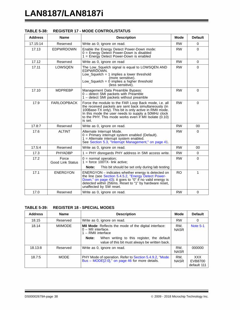
LAN8187/LAN8187i
TABLE 5-38: REGISTER 17 - MODE CONTROL/STATUS
Address Name Description Mode Default
17.15:14 Reserved Write as 0; ignore on read. RW 0
17.13 EDPWRDOWN Enable the Energy Detect Power-Down mode:0 = Energy Detect Power-Down is disabled1 = Energy Detect Power-Down is enabled
RW 0
17.12 Reserved Write as 0, ignore on read RW 0
17.11 LOWSQEN The Low_Squelch signal is equal to LOWSQEN AND EDPWRDOWN.Low_Squelch = 1 implies a lower threshold
(more sensitive).Low_Squelch = 0 implies a higher threshold
(less sensitive).
RW 0
17.10 MDPREBP Management Data Preamble Bypass:0 – detect SMI packets with Preamble1 – detect SMI packets without preamble
RW 0
17.9 FARLOOPBACK Force the module to the FAR Loop Back mode, i.e. all the received packets are sent back simultaneously (in 100Base-TX only). This bit is only active in RMII mode. In this mode the user needs to supply a 50MHz clock to the PHY. This mode works even if MII Isolate (0.10) is set.
RW 0
17.8:7 Reserved Write as 0, ignore on read. RW 00
17.6 ALTINT Alternate Interrupt Mode.0 = Primary interrupt system enabled (Default).1 = Alternate interrupt system enabled.See Section 5.3, "Interrupt Management," on page 41.
RW 0
17.5:4 Reserved Write as 0, ignore on read. RW 00
17.3 PHYADBP 1 = PHY disregards PHY address in SMI access write. RW 0
17.2 ForceGood Link Status
0 = normal operation;1 = force 100TX- link active;
Note: This bit should be set only during lab testing
RW 0
17.1 ENERGYON ENERGYON – indicates whether energy is detected on the line (see Section 5.4.5.2, "Energy Detect Power-Down," on page 43); it goes to “0” if no valid energy is detected within 256ms. Reset to “1” by hardware reset, unaffected by SW reset.
RO 1
17.0 Reserved Write as 0, ignore on read. RW 0
TABLE 5-39: REGISTER 18 - SPECIAL MODES
Address Name Description Mode Default
18.15 Reserved Write as 0, ignore on read. RW 0
18.14 MIIMODE MII Mode: Reflects the mode of the digital interface:0 – MII interface.1 – RMII interface
Note: When writing to this register, the defaultvalue of this bit must always be written back.
RW, NASR
Note 5-1
18.13:8 Reserved Write as 0, ignore on read. RW, NASR
000000
18.7:5 MODE PHY Mode of operation. Refer to Section 5.4.9.2, "Mode Bus – MODE[2:0]," on page 46 for more details.
RW, NASR
XXXEVB8700
default 111
DS00002679A-page 38 2009 - 2018 Microchip Technology Inc.

LAN8187/LAN8187i
Note 5-1 The default value of this field is determined by the strapping of the GPO0/RMII pin. Refer to Section4.6.3, "MII vs. RMII Configuration," on page 21 for additional information.
18.4:0 PHYAD PHY Address.The PHY Address is used for the SMI address and for the initialization of the Cipher (Scrambler) key. Refer to Section 5.4.9.1, "Physical Address Bus - PHYAD[4:0]," on page 46 for more details.
RW, NASR
PHYADEVB8700
default 11111
TABLE 5-40: REGISTER 26 - SYMBOL ERROR COUNTER
Address Name Description Mode Default
26.15:0 Sym_Err_Cnt 100Base-TX receiver-based error register that increments when an invalid code symbol is received including IDLE symbols. The counter is incremented only once per packet, even when the received packet contains more than one symbol error. The 16-bit register counts up to 65,536 (216) and rolls over to 0 if incremented beyond that value. This register is cleared on reset, but is not cleared by reading the register. It does not increment in 10Base-T mode.
RO 0
TABLE 5-41: REGISTER 27 - SPECIAL CONTROL/STATUS INDICATIONS
Address Name Description Mode Default
27.15 AMDIXIOCTRL Enables the external AMDIX and CH_SELECT pins0 - External pins AMDIX_EN and CH_SELECT control
the AMDIX.1 - Internal bits 27.14 and 27.13 control the AMDIX.
Note: Please see Table 4-3, “Auto-MDIX Control,”on page 24
RW 0
27.14 AMDIX_ENABLE HP Auto-MDIX control0 - Auto-MDIX disabled (use 27.13 to control channel)1 - Auto-MDIX enable
Note: This bit can only be used if 27.15 is a 1.
RW 0
27.13 CH_SELECT Manual Channel Select0 - MDI -TX transmits RX receives1 - MDIX -TX receives RX transmits
Note: This bit can only be used if 27.15 is a 1 and27.14 is a 0.
RW 0
27.12 Reserved Write as 0. Ignore on read. RW 0
27:11 SQEOFF Disable the SQE (Signal Quality Error) test (Heartbeat):0 - SQE test is enabled.1 - SQE test is disabled.
RW, NASR
0
27.10:5 Reserved Write as 0. Ignore on read. RW 000000
27.4 XPOL Polarity state of the 10Base-T:0 - Normal polarity1 - Reversed polarity
RO 0
27.3:0 Reserved Reserved RO XXXXb
TABLE 5-42: REGISTER 28 - SPECIAL INTERNAL TESTABILITY CONTROLS
Address Name Description Mode Default
28.15:0 Reserved Do not write to this register. Ignore on read. RW N/A
TABLE 5-39: REGISTER 18 - SPECIAL MODES (CONTINUED)
Address Name Description Mode Default
2009 - 2018 Microchip Technology Inc. DS00002679A-page 39

LAN8187/LAN8187i
TABLE 5-43: REGISTER 29 - INTERRUPT SOURCE FLAGS
Address Name Description Mode Default
29.15:8 Reserved Ignore on read. RO/LH
0
29.7 INT7 1 = ENERGYON generated 0 = not source of interrupt
RO/LH
X
29.6 INT6 1 = Auto-Negotiation complete 0 = not source of interrupt
RO/LH
X
29.5 INT5 1 = Remote Fault Detected 0 = not source of interrupt
RO/LH
X
29.4 INT4 1 = Link Down (link status negated) 0 = not source of interrupt
RO/LH
X
29.3 INT3 1 = Auto-Negotiation LP Acknowledge0 = not source of interrupt
RO/LH
X
29.2 INT2 1 = Parallel Detection Fault 0 = not source of interrupt
RO/LH
X
29.1 INT1 1 = Auto-Negotiation Page Received 0 = not source of interrupt
RO/LH
X
29.0 Reserved Ignore on read. RO/LH
0
TABLE 5-44: REGISTER 30 - INTERRUPT MASK
Address Name Description Mode Default
30.15:8 Reserved Write as 0; ignore on read. RO 0
30.7:0 Mask Bits 1 = interrupt source is enabled0 = interrupt source is masked
RW 0
TABLE 5-45: REGISTER 31 - PHY SPECIAL CONTROL/STATUS
Address Name Description Mode Default
31.15 Reserved Do not write to this register. Ignore on read. RW 0
31.14 Reserved
31.13 Reserved Must be set to 0 RW 0
31.12 Autodone Auto-negotiation done indication:0 = Auto-negotiation is not done or disabled (or not
active)1 = Auto-negotiation is done
RO 0
31.11 Reserved Write as 0, ignore on Read. RW X
31.10 Reserved Reserved RW 0
31.9:7 GPO[2:0] General Purpose Output connected to signals GPO[2:0] RW 0
31.6 Enable 4B5B 0 = Bypass encoder/decoder.1 = enable 4B5B encoding/decoding.MAC Interface must be configured in MII mode.
RW 1
31.5 Reserved Write as 0, ignore on Read. RW 0
31.4:2 Speed Indication HCDSPEED value:[001]=10Mbps Half-duplex[101]=10Mbps Full-duplex[010]=100Base-TX Half-duplex[110]=100Base-TX Full-duplex
RO 000
DS00002679A-page 40 2009 - 2018 Microchip Technology Inc.

LAN8187/LAN8187i
5.3 Interrupt Management
The Management interface supports an interrupt capability that is not a part of the IEEE 802.3 specification. It generatesan active low asynchronous interrupt signal on the nINT output whenever certain events are detected as setup by theInterrupt Mask Register 30.
The Interrupt system on the Microchip LAN8187/8187i has two modes, a Primary Interrupt mode and an AlternativeInterrupt mode. Both systems will assert the nINT pin low when the corresponding mask bit is set, the difference is howthey de-assert the output interrupt signal nINT.
The Primary interrupt mode is the default interrupt mode after a power-up or hard reset, the Alternative interrupt modewould need to be setup again after a power-up or hard reset.
5.3.1 PRIMARY INTERRUPT SYSTEM
The Primary Interrupt system is the default interrupt mode, (Bit 17.6 = ‘0’). The Primary Interrupt System is alwaysselected after power-up or hard reset.
To set an interrupt, set the corresponding mask bit in the interrupt Mask register 30 (see Table 5-46). Then when theevent to assert nINT is true, the nINT output will be asserted.
When the corresponding Event to De-Assert nINT is true, then the nINT will be de-asserted.
Note 5-2 If the mask bit is enabled and nINT has been de-asserted while ENERGYON is still high, nINT willassert for 256 ms, approximately one second after ENERGYON goes low when the Cable isunplugged. To prevent an unexpected assertion of nINT, the ENERGYON interrupt mask shouldalways be cleared as part of the ENERGYON interrupt service routine.
31.1 Reserved Write as 0; ignore on Read RW 0
31.0 Scramble Disable 0 = enable data scrambling 1 = disable data scrambling,
RW 0
TABLE 5-46: INTERRUPT MANAGEMENT TABLE
Mask Interrupt Source Flag Interrupt SourceEvent to
Assert nINTEvent to
De-Assert nINT
30.7 29.7 ENERGYON 17.1 ENERGYON Rising 17.1(Note 5-2)
Falling 17.1 orReading register 29
30.6 29.6 Auto-Negotiation complete
1.5 Auto-Negotiate Complete
Rising 1.5 Falling 1.5 orReading register 29
30.5 29.5 Remote Fault Detected 1.4 Remote Fault Rising 1.4 Falling 1.4, or Reading register 1 or Reading register 29
30.4 29.4 Link Down 1.2 Link Status Falling 1.2 Reading register 1 orReading register 29
30.3 29.3 Auto-Negotiation LP Acknowledge
5.14 Acknowledge Rising 5.14 Falling 5.14 orRead register 29
30.2 29.2 Parallel Detection Fault 6.4 Parallel Detection Fault
Rising 6.4 Falling 6.4 or Reading register 6, orReading register 29 orRe-AutoNegotiate or
Link down
30.1 29.1 Auto-Negotiation Page Received
6.1 Page Received Rising 6.1 Falling of 6.1 orReading register 6, orReading register 29
Re-AutoNegotiate, orLink Down.
TABLE 5-45: REGISTER 31 - PHY SPECIAL CONTROL/STATUS (CONTINUED)
Address Name Description Mode Default
2009 - 2018 Microchip Technology Inc. DS00002679A-page 41

LAN8187/LAN8187i
5.3.2 ALTERNATE INTERRUPT SYSTEM
The Alternative method is enabled by writing a ‘1’ to 17.6 (ALTINT).
To set an interrupt, set the corresponding bit of the in the Mask Register 30, (see Table 5-47).
To Clear an interrupt, either clear the corresponding bit in the Mask Register (30), this will de-assert the nINT output, orClear the Interrupt Source, and write a ‘1’ to the corresponding Interrupt Source Flag. Writing a ‘1’ to the Interrupt SourceFlag will cause the state machine to check the Interrupt Source to determine if the Interrupt Source Flag should clear orstay as a ‘1’. If the Condition to De-Assert is true, then the Interrupt Source Flag is cleared, and the nINT is also de-asserted. If the Condition to De-Assert is false, then the Interrupt Source Flag remains set, and the nINT remainsasserted.
5.3.2.1 Example Alternative Interrupts system
For example 30.7 is set to ‘1’ to enable the ENERGYON interrupt. After a cable is plugged in, ENERGYON (17.1) goesactive and nINT will be asserted low.
To de-assert the nINT interrupt output, either.
1. Clear the ENERGYON bit (17.1), by removing the cable, then writing a ‘1’ to register 29.7.
- Or -
2. Clear the Mask bit 30.1
5.4 Miscellaneous Functions
5.4.1 CARRIER SENSE
The carrier sense is output on CRS. CRS is a signal defined by the MII specification in the IEEE 802.3u standard. ThePHY asserts CRS based only on receive activity whenever the PHY is either in repeater mode or full-duplex mode. Oth-erwise the PHY asserts CRS based on either transmit or receive activity.
Note: The ENERGYON bit 17.1 is defaulted to a ‘1’ at the start of the signal acquisition process, therefore theInterrupt source flag 29.7 will also read as a ‘1’ at power-up. If no signal is present, then both 17.1 and 29.7will clear within a few milliseconds.
TABLE 5-47: ALTERNATIVE INTERRUPT SYSTEM MANAGEMENT TABLE
Mask Interrupt Source Flag Interrupt SourceEvent to Assert
nINTCondition to
De-AssertBit to Clear
nINT
30.7 29.7 ENERGYON 17.1 ENERGYON Rising 17.1 17.1 low 29.7
30.6 29.6 Auto-Negotiation complete
1.5 Auto-Negotiate Complete
Rising 1.5 1.5 low 29.6
30.5 29.5 Remote Fault Detected 1.4 Remote Fault Rising 1.4 1.4 low 29.5
30.4 29.4 Link Down 1.2 Link Status Falling 1.2 1.2 high 29.4
30.3 29.3 Auto-Negotiation LP Acknowledge
5.14 Acknowledge Rising 5.14 5.14 low 29.3
30.2 29.2 Parallel Detection Fault 6.4 Parallel Detection Fault
Rising 6.4 6.4 low 29.2
30.1 29.1 Auto-Negotiation Page Received
6.1 Page Received Rising 6.1 6.1 low 29.1
Note: The ENERGYON bit 17.1 is defaulted to a ‘1’ at the start of the signal acquisition process, therefore theInterrupt source flag 29.7 will also read as a ‘1’ at power-up. If no signal is present, then both 17.1 and 29.7will clear within a few milliseconds.
DS00002679A-page 42 2009 - 2018 Microchip Technology Inc.

LAN8187/LAN8187i
The carrier sense logic uses the encoded, unscrambled data to determine carrier activity status. It activates carriersense with the detection of 2 non-contiguous zeros within any 10 bit span. Carrier sense terminates if a span of 10 con-secutive ones is detected before a /J/K/ Start-of Stream Delimiter pair. If an SSD pair is detected, carrier sense isasserted until either /T/R/ End–of-Stream Delimiter pair or a pair of IDLE symbols is detected. Carrier is negated afterthe /T/ symbol or the first IDLE. If /T/ is not followed by /R/, then carrier is maintained. Carrier is treated similarly for IDLEfollowed by some non-IDLE symbol.
5.4.2 COLLISION DETECT
A collision is the occurrence of simultaneous transmit and receive operations. The COL output is asserted to indicatethat a collision has been detected. COL remains active for the duration of the collision. COL is changed asynchronouslyto both RX_CLK and TX_CLK. The COL output becomes inactive during full duplex mode.
COL may be tested by setting register 0, bit 7 high. This enables the collision test. COL will be asserted within 512 bittimes of TX_EN rising and will be de-asserted within 4 bit times of TX_EN falling.
In 10M mode, COL pulses for approximately 10 bit times (1us), 2us after each transmitted packet (de-assertion ofTX_EN). This is the Signal Quality Error (SQE) signal and indicates that the transmission was successful. The user candisable this pulse by setting bit 11 in register 27.
5.4.3 ISOLATE MODE
The PHY data paths may be electrically isolated from the MII by setting register 0, bit 10 to a logic one. In isolation mode,the PHY does not respond to the TXD, TX_EN and TX_ER inputs. The PHY still responds to management transactions.
Isolation provides a means for multiple PHYs to be connected to the same MII without contention occurring. The PHYis not isolated on power-up (bit 0:10 = 0).
5.4.4 LINK INTEGRITY TEST
The LAN8187/LAN8187i performs the link integrity test as outlined in the IEEE 802.3u (Clause 24-15) Link Monitor statediagram. The link status is multiplexed with the 10Mbps link status to form the reportable link status bit in Serial Man-agement Register 1, and is driven to the LINK LED.
The DSP indicates a valid MLT-3 waveform present on the RXP and RXN signals as defined by the ANSI X3.263 TP-PMD standard, to the Link Monitor state-machine, using internal signal called DATA_VALID. When DATA_VALID isasserted the control logic moves into a Link-Ready state, and waits for an enable from the Auto Negotiation block. Whenreceived, the Link-Up state is entered, and the Transmit and Receive logic blocks become active. Should Auto Negoti-ation be disabled, the link integrity logic moves immediately to the Link-Up state, when the DATA_VALID is asserted.
Note that to allow the line to stabilize, the link integrity logic will wait a minimum of 330 sec from the time DATA_VALIDis asserted until the Link-Ready state is entered. Should the DATA_VALID input be negated at any time, this logic willimmediately negate the Link signal and enter the Link-Down state.
When the 10/100 digital block is in 10Base-T mode, the link status is from the 10Base-T receiver logic.
5.4.5 POWER-DOWN MODES
There are 2 power-down modes for the Phy:
5.4.5.1 General Power-Down
This power-down is controlled by register 0, bit 11. In this mode the entire PHY, except the management interface, ispowered-down and stays in that condition as long as bit 0.11 is HIGH. When bit 0.11 is cleared, the PHY powers up andis automatically reset.
5.4.5.2 Energy Detect Power-Down
This power-down mode is activated by setting bit 17.13 to 1. In this mode when no energy is present on the line the PHYis powered down, except for the management interface, the SQUELCH circuit and the ENERGYON logic. The ENER-GYON logic is used to detect the presence of valid energy from 100Base-TX, 10Base-T, or Auto-negotiation signals
In this mode, when the ENERGYON signal is low, the PHY is powered-down, and nothing is transmitted. When energyis received - link pulses or packets - the ENERGYON signal goes high, and the PHY powers-up. It automatically resetsitself into the state it had prior to power-down, and asserts the nINT interrupt if the ENERGYON interrupt is enabled.The first and possibly the second packet to activate ENERGYON may be lost.
When 17.13 is low, energy detect power-down is disabled.
2009 - 2018 Microchip Technology Inc. DS00002679A-page 43

LAN8187/LAN8187i
5.4.6 RESET
The LAN8187/LAN8187i has 3 reset sources:
Hardware reset (HWRST): connected to the nRST input. At power up, nRST must not go high until after the VDDIOand VDD_CORE supplies are stable, as shown in Figure 5-1.
To initiate a hardware reset, nRST must be held LOW for at least 100 us to ensure that the Phy is properly reset, asshown in Figure 6-10.
During a Hardware reset, an external clock must be supplied to the CLKIN signal.
Software (SW) reset: Activated by writing register 0, bit 15 high. This signal is self- clearing. After the register-write,internal logic extends the reset by 256µs to allow PLL-stabilization before releasing the logic from reset.
The IEEE 802.3u standard, clause 22 (22.2.4.1.1) states that the reset process should be completed within 0.5s fromthe setting of this bit.
Power-Down reset: Automatically activated when the PHY comes out of power-down mode. The internal power-downreset is extended by 256µs after exiting the power-down mode to allow the PLLs to stabilize before the logic is releasedfrom reset.
These 3 reset sources are combined together in the digital block to create the internal “general reset”, SYSRST, whichis an asynchronous reset and is active HIGH. This SYSRST directly drives the PCS, DSP and MII blocks. It is also inputto the Central Bias block in order to generate a short reset for the PLLs.
The SMI mechanism and registers are reset only by the Hardware and Software resets. During Power-Down, the SMIregisters are not reset. Note that some SMI register bits are not cleared by Software reset – these are marked “NASR”in the register tables.
For several microseconds after coming out of reset, the MII will run at 2.5 MHz. After that it will switch to 25 MHz if auto-negotiation is enabled.
5.4.7 LED DESCRIPTION
The PHY provides four LED signals. These provide a convenient means to determine the mode of operation of the Phy.All LED signals are either active high or active low.
The four LED signals can be either active-high or active-low. Polarity depends upon the Phy address latched in on reset.The LAN8187/LAN8187i senses each Phy address bit and changes the polarity of the LED signal accordingly. If theaddress bit is set as level “1”, the LED polarity will be set to an active-low. If the address bit is set as level “0”, the LEDpolarity will be set to an active-high.
The ACTIVITY LED output is driven active when CRS is active (high). When CRS becomes inactive, the Activity LEDoutput is extended by 128ms.
The LINK LED output is driven active whenever the PHY detects a valid link. The use of the 10Mbps or 100Mbps linktest status is determined by the condition of the internally determined speed selection.
The SPEED100 LED output is driven active when the operating speed is 100Mbit/s or during Auto-negotiation. This LEDwill go inactive when the operating speed is 10Mbit/s or during line isolation (register 31 bit 5).
The Full-Duplex LED output is driven active low when the link is operating in Full-Duplex mode.
FIGURE 5-1: RESET TIMING DIAGRAM
VDD_CORE Starts nRST Released
0V
3.3V
1.8V
VDD33 Starts
DS00002679A-page 44 2009 - 2018 Microchip Technology Inc.

LAN8187/LAN8187i
5.4.8 LOOPBACK OPERATION
The LAN8187/LAN8187i may be configured for near-end loopback and far loopback.
5.4.8.1 Near-end Loopback
Near-end loopback is a mode that sends the digital transmit data back out the receive data signals for testing purposesas indicated by the blue arrows in Figure 5-2.The near-end loopback mode is enabled by setting bit register 0 bit 14 tologic one.
A large percentage of the digital circuitry is operational near-end loopback mode, because data is routed through thePCS and PMA layers into the PMD sublayer before it is looped back. The COL signal will be inactive in this mode, unlesscollision test (bit 0.7) is active. The transmitters are powered down, regardless of the state of TXEN.
5.4.8.2 Far Loopback
Far loopback is a special test mode for MDI (analog) loopback as indicated by the blue arrows in Figure 5-3. The farloopback mode is enabled by setting bit register 17 bit 9 to logic one. In this mode, data that is received from the linkpartner on the MDI is looped back out to the link partner. The digital interface signals on the local MAC interface areisolated.
FIGURE 5-2: NEAR-END LOOPBACK BLOCK DIAGRAM
Note: This special test mode is only available when operating in RMII mode.
FIGURE 5-3: FAR LOOPBACK BLOCK DIAGRAM
Ethernet Transceiver
10/100Ethernet
MAC
CAT-5XFMR
Digital
RXD
TXD
Analog
RX
TXX
X
Far-end system
Ethernet Transceiver
10/100Ethernet
MAC
CAT-5XFMR
Digital
RXD
TXD
Analog
RX
TXLink
Partner
X
X
2009 - 2018 Microchip Technology Inc. DS00002679A-page 45

LAN8187/LAN8187i
5.4.8.3 Connector Loopback
The LAN8187/LAN8187i maintains reliable transmission over very short cables, and can be tested in a connector loop-back as shown in Figure 5-4. An RJ45 loopback cable can be used to route the transmit signals an the output of thetransformer back to the receiver inputs, and this loopback will work at both 10 and 100.
5.4.9 CONFIGURATION SIGNALS
The PHY has 11 configuration signals whose inputs should be driven continuously, either by external logic or externalpull-up/pull-down resistors.
5.4.9.1 Physical Address Bus - PHYAD[4:0]
The PHYAD[4:0] signals are driven high or low to give each PHY a unique address. This address is latched into an inter-nal register at end of hardware reset. In a multi-PHY application (such as a repeater), the controller is able to manageeach PHY via the unique address. Each PHY checks each management data frame for a matching address in the rel-evant bits. When a match is recognized, the PHY responds to that particular frame. The PHY address is also used toseed the scrambler. In a multi-PHY application, this ensures that the scramblers are out of synchronization and dis-perses the electromagnetic radiation across the frequency spectrum.
5.4.9.2 Mode Bus – MODE[2:0]
The MODE[2:0] bus controls the configuration of the 10/100 digital block. When the nRST pin is de-asserted, the registerbit values are loaded according to the MODE[2:0] pins. The 10/100 digital block is then configured by the register bitvalues. When a soft reset occurs (bit 0.15) as described in Table 5-30, the configuration of the 10/100 digital block iscontrolled by the register bit values, and the MODE[2:0] pins have no affect.
FIGURE 5-4: CONNECTOR LOOPBACK BLOCK DIAGRAM
Ethernet Transceiver
10/100Ethernet
MACXFMR
Digital
RXD
TXD
Analog
RX
TX12345678
RJ45 Loopback Cable.Created by connecting pin 1 to pin 3 and connecting pin 2 to pin 6.
DS00002679A-page 46 2009 - 2018 Microchip Technology Inc.
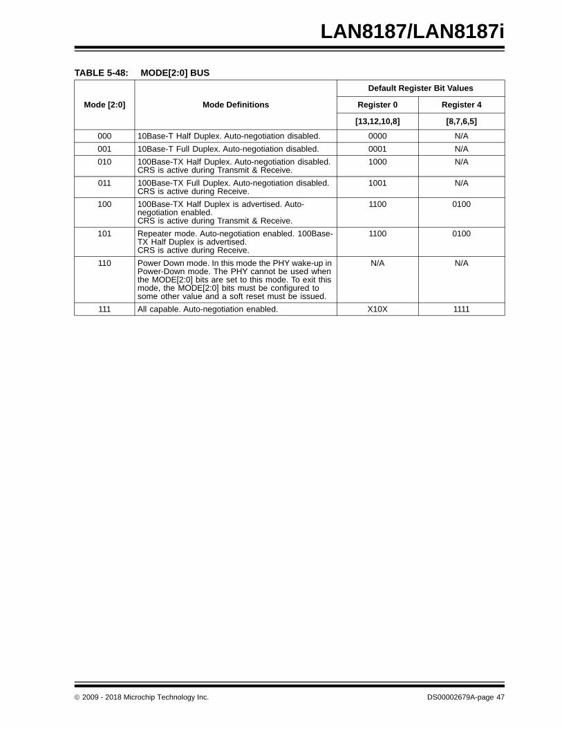
LAN8187/LAN8187i
TABLE 5-48: MODE[2:0] BUS
Mode [2:0] Mode Definitions
Default Register Bit Values
Register 0 Register 4
[13,12,10,8] [8,7,6,5]
000 10Base-T Half Duplex. Auto-negotiation disabled. 0000 N/A
001 10Base-T Full Duplex. Auto-negotiation disabled. 0001 N/A
010 100Base-TX Half Duplex. Auto-negotiation disabled.CRS is active during Transmit & Receive.
1000 N/A
011 100Base-TX Full Duplex. Auto-negotiation disabled.CRS is active during Receive.
1001 N/A
100 100Base-TX Half Duplex is advertised. Auto-negotiation enabled.CRS is active during Transmit & Receive.
1100 0100
101 Repeater mode. Auto-negotiation enabled. 100Base-TX Half Duplex is advertised. CRS is active during Receive.
1100 0100
110 Power Down mode. In this mode the PHY wake-up in Power-Down mode. The PHY cannot be used when the MODE[2:0] bits are set to this mode. To exit this mode, the MODE[2:0] bits must be configured to some other value and a soft reset must be issued.
N/A N/A
111 All capable. Auto-negotiation enabled. X10X 1111
2009 - 2018 Microchip Technology Inc. DS00002679A-page 47

LAN8187/LAN8187i
6.0 AC ELECTRICAL CHARACTERISTICS
The timing diagrams and limits in this section define the requirements placed on the external signals of theLAN8187/LAN8187i.
6.1 Serial Management Interface (SMI) Timing
The Serial Management Interface is used for status and control as described in Section 4.13.
FIGURE 6-1: SMI TIMING DIAGRAM
TABLE 6-1: SMI TIMING VALUES
Parameter Description MIN TYP MAX Units Notes
T1.1 MDC minimum cycle time 400 ns
T1.2 MDC to MDIO (Read from PHY) delay
0 300 ns
T1.3 MDIO (Write to PHY) to MDC setup 10 ns
T1.4 MDIO (Write to PHY) to MDC hold 10 ns
Clock -MDC
Data Out - MDIO
T1.2
Valid Data(Read from PHY)
T1.1
T1.3 T1.4
Data In - MDIO
Valid Data(Write to PHY)
DS00002679A-page 48 2009 - 2018 Microchip Technology Inc.
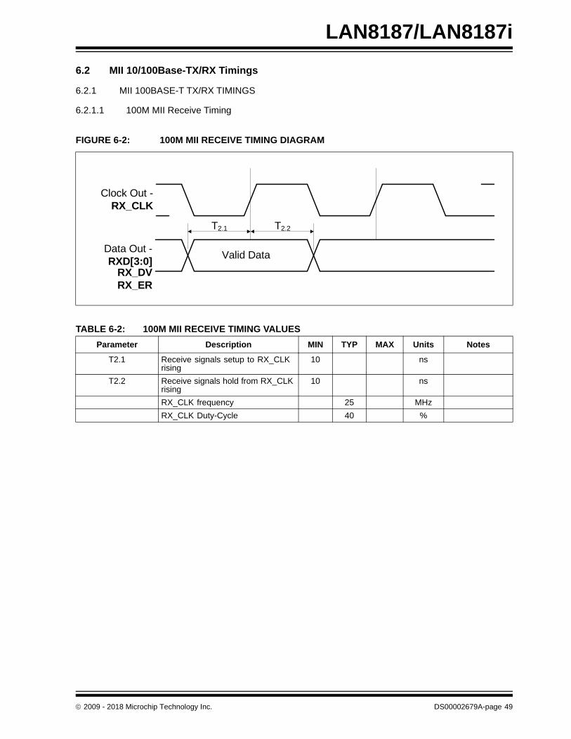
LAN8187/LAN8187i
6.2 MII 10/100Base-TX/RX Timings
6.2.1 MII 100BASE-T TX/RX TIMINGS
6.2.1.1 100M MII Receive Timing
FIGURE 6-2: 100M MII RECEIVE TIMING DIAGRAM
TABLE 6-2: 100M MII RECEIVE TIMING VALUES
Parameter Description MIN TYP MAX Units Notes
T2.1 Receive signals setup to RX_CLK rising
10 ns
T2.2 Receive signals hold from RX_CLK rising
10 ns
RX_CLK frequency 25 MHz
RX_CLK Duty-Cycle 40 %
Clock Out -RX_CLK
Data Out - RXD[3:0]
T2.1
RX_DVRX_ER
T2.2
Valid Data
2009 - 2018 Microchip Technology Inc. DS00002679A-page 49

LAN8187/LAN8187i
6.2.1.2 100M MII Transmit Timing
FIGURE 6-3: 100M MII TRANSMIT TIMING DIAGRAM
TABLE 6-3: 100M MII TRANSMIT TIMING VALUES
Parameter Description MIN TYP MAX Units Notes
T3.1 Transmit signals required setup to TX_CLK rising
12 ns
Transmit signals required hold after TX_CLK rising
0 ns
TX_CLK frequency 25 MHz
TX_CLK Duty-Cycle 40 %
Clock Out -TX_CLK
Data Out - TXD[3:0]
T3.1
TX_ENTX_ER
Valid Data
DS00002679A-page 50 2009 - 2018 Microchip Technology Inc.

LAN8187/LAN8187i
6.2.2 MII 10BASE-T TX/RX TIMINGS
6.2.2.1 10M MII Receive Timing
FIGURE 6-4: 10M MII RECEIVE TIMING DIAGRAM
TABLE 6-4: 10M MII RECEIVE TIMING VALUES
Parameter Description MIN TYP MAX Units Notes
T4.1 Receive signals setup to RX_CLK rising
10 ns
T4.2 Receive signals hold from RX_CLK rising
10 ns
RX_CLK frequency 2.5 MHz
RX_CLK Duty-Cycle 40 %
Clock Out -RX_CLK
Data Out - RXD[3:0]
T4.1
RX_DV
T4.2
Valid Data
2009 - 2018 Microchip Technology Inc. DS00002679A-page 51

LAN8187/LAN8187i
6.2.2.2 10M MII Transmit Timing
FIGURE 6-5: 10M MII TRANSMIT TIMING DIAGRAMS
TABLE 6-5: 10M MII TRANSMIT TIMING VALUES
Parameter Description MIN TYP MAX Units Notes
T5.1 Transmit signals required setup to TX_CLK rising
12 ns
Transmit signals required hold after TX_CLK rising
0 ns
TX_CLK frequency 2.5 MHz
TX_CLK Duty-Cycle 50 %
Clock Out -TX_CLK
Data Out - TXD[3:0]
T5.1
TX_EN
Valid Data
DS00002679A-page 52 2009 - 2018 Microchip Technology Inc.

LAN8187/LAN8187i
6.3 RMII 10/100Base-TX/RX Timings
6.3.1 RMII 100BASE-T TX/RX TIMINGS
6.3.1.1 100M RMII Receive Timing
FIGURE 6-6: 100M RMII RECEIVE TIMING DIAGRAM
TABLE 6-6: 100M RMII RECEIVE TIMING VALUES
Parameter Description MIN TYP MAX Units Notes
T6.1 Output delay from rising edge of CLKIN to receive signals output valid
2 10 ns
CLKIN frequency 50 MHz
Clock In -CLKIN
Data Out - RXD[1:0]CRS_DV
Valid Data
T6.1
2009 - 2018 Microchip Technology Inc. DS00002679A-page 53

LAN8187/LAN8187i
6.3.1.2 100M RMII Transmit Timing
FIGURE 6-7: 100M RMII TRANSMIT TIMING DIAGRAM
TABLE 6-7: 100M RMII TRANSMIT TIMING VALUES
Parameter Description MIN TYP MAX Units Notes
T8.1 Transmit signals required setup to rising edge of CLKIN
2 ns
T8.2 Transmit signals required hold after rising edge of REF_CLK
1.5 ns
CLKIN frequency 50 MHz
Clock In -CLKIN
Data Out - TXD[1:0]
T8.1
TX_EN
T8.2
Valid Data
DS00002679A-page 54 2009 - 2018 Microchip Technology Inc.

LAN8187/LAN8187i
6.3.2 RMII 10BASE-T TX/RX TIMINGS
6.3.2.1 10M RMII Receive Timing
FIGURE 6-8: 10M RMII RECEIVE TIMING DIAGRAM
TABLE 6-8: 10M RMII RECEIVE TIMING VALUES
Parameter Description MIN TYP MAX Units Notes
T9.1 Output delay from rising edge of CLKIN to receive signals output valid
2 10 ns
CLKIN frequency 50 MHz
Clock In -CLKIN
Data Out - RXD[1:0]CRS_DV
Valid Data
T9.1
2009 - 2018 Microchip Technology Inc. DS00002679A-page 55

LAN8187/LAN8187i
6.3.2.2 10M RMII Transmit Timing
6.4 RMII CLKIN Timing
FIGURE 6-9: 10M RMII TRANSMIT TIMING DIAGRAM
TABLE 6-9: 10M RMII TRANSMIT TIMING VALUES
Parameter Description MIN TYP MAX Units Notes
T10.1 Transmit signals required setup to rising edge of CLKIN
4 ns
T10.2 Transmit signals required hold after rising edge of REF_CLK
2 ns
CLKIN frequency 50 MHz
TABLE 6-10: RMII CLKIN (REF_CLK) TIMING VALUES
Parameter Description MIN TYP MAX Units Notes
CLKIN frequency 50 MHz
CLKIN Frequency Drift ± 50 ppm
CLKIN Duty Cycle 40 60 %
CLKIN Jitter 150 psec p-p – not RMS
Clock In -CLKIN
Data Out - TXD[1:0]
T10.1
TX_EN
T10.2
Valid Data
DS00002679A-page 56 2009 - 2018 Microchip Technology Inc.

LAN8187/LAN8187i
6.5 Reset Timing
FIGURE 6-10: RESET TIMING DIAGRAM
TABLE 6-11: RESET TIMING VALUES
Parameter Description MIN TYP MAX Units Notes
T11.1 Reset Pulse Width 100 us
T11.2 Configuration input setup to nRST rising
200 ns
T11.3 Configuration input hold after nRST rising
2 ns
T11.4 Output Drive after nRST rising 3 800 ns 20 clock cycles for 25 MHz clock
- or -40 clock cycles for
50MHz clock
nRST
ConfigurationSignals
T11.1
T11.4
Output drive
T11.2 T11.3
2009 - 2018 Microchip Technology Inc. DS00002679A-page 57

LAN8187/LAN8187i
6.6 Clock Circuit
LAN8187/LAN8187i can accept either a 25MHz crystal or a 25MHz single-ended clock oscillator (±50ppm) input foroperation in MII mode. If the single-ended clock oscillator method is implemented, XTAL2 should be left unconnectedand XTAL1/CLKIN should be driven with a nominal 0-3.3V clock signal. The user is required to supply a 50MHz single-ended clock for RMII operation. The input clock duty cycle is 40% minimum, 50% typical and 60% maximum. SeeTable 6-12 for the recommended crystal specifications.
Note 6-1 The maximum allowable values for Frequency Tolerance and Frequency Stability are applicationdependent. Since any particular application must meet the IEEE ±50 PPM Total PPM Budget, thecombination of these two values must be approximately ±45 PPM (allowing for aging).
Note 6-2 Frequency Deviation Over Time is also referred to as Aging.
Note 6-3 The total deviation for the Transmitter Clock Frequency is specified by IEEE 802.3u as ±100 PPM.
Note 6-4 0oC for commercial version, -40oC for industrial version.
Note 6-5 +70oC for commercial version, +85oC for industrial version.
Note 6-6 This number includes the pad, the bond wire and the lead frame. PCB capacitance is not includedin this value. The XTAL1/CLKIN pin, XTAL2 pin and PCB capacitance values are required toaccurately calculate the value of the two external load capacitors. The total load capacitance mustbe equivalent to what the crystal expects to see in the circuit so that the crystal oscillator will operateat 25.000 MHz.
TABLE 6-12: LAN8187/LAN8187I CRYSTAL SPECIFICATIONS
Parameter Symbol MIN NOM MAX Units Notes
Crystal Cut AT, typ
Crystal Oscillation Mode Fundamental Mode
Crystal Calibration Mode Parallel Resonant Mode
Frequency Ffund - 25.000 - MHz
Frequency Tolerance @ 25oC Ftol - - ±50 PPM Note 6-1
Frequency Stability Over Temp Ftemp - - ±50 PPM Note 6-1
Frequency Deviation Over Time Fage - +/-3 to 5 - PPM Note 6-2
Total Allowable PPM Budget - - ±50 PPM Note 6-3
Shunt Capacitance CO - 7 typ - pF
Load Capacitance CL - 20 typ - pF
Drive Level PW 0.5 - - mW
Equivalent Series Resistance R1 - - 30 Ohm
Operating Temperature Range Note 6-4 - Note 6-5 oC
LAN8187/LAN8187i XTAL1/CLKIN Pin Capacitance
- 3 typ - pF Note 6-6
LAN8187/LAN8187i XTAL2 Pin Capacitance
- 3 typ - pF Note 6-6
DS00002679A-page 58 2009 - 2018 Microchip Technology Inc.

LAN8187/LAN8187i
7.0 DC ELECTRICAL CHARACTERISTICS
7.1 DC Characteristics
7.1.1 MAXIMUM RATINGS
Stresses beyond those listed in Table 7-1 may cause permanent damage to the device. Exposure to absolute maximumrating conditions for extended periods may affect device reliability.
7.1.1.1 Human Body Model (HBM) Performance
HBM testing verifies the ability to withstand the ESD strikes like those that occur during handling and manufacturing.The device must work normally after the stress has ended, meaning no latch-up on any pins. All pins on the LAN8187provide +/- 8kV HBM protection.
7.1.1.2 EN61000-4-2 Performance
The EN61000-4-2 ESD specification is an international standard that addresses system-level immunity to ESD strikeswhile the end equipment is operational. In contrast, the HBM ESD tests are performed at the device level with the devicepowered down.
In addition to defining the ESD tests, EN61000-4-2 also categorizes the impact to equipment operation when the strikeoccurs (ESD Result Classification). The LAN8187 maintains an ESD Result Classification 1 or 2 when subjected to anEN61000-4-2 (level 4) ESD strike.
Both air discharge and contact discharge test techniques for applying stress conditions are defined by the EN61000-4-2 ESD document.
TABLE 7-1: MAXIMUM CONDITIONS
Parameter Conditions MIN TYP MAX Units Comment
VDD33,VDDIO Power pins to all other pins. -0.5 +3.6 V
Digital IO To VSS ground -0.5 +3.6 V Table 7-5, “MII Bus Interface Signals,” on page 62
VSS VSS to all other pins -0.5 +4.0 V
Operating Temperature
LAN8187-JT 0 +70 C Commercial temperature parts.
Operating Temperature
LAN8187i-JT -40 +85 C Industrial temperature parts.
Storage Temperature
-55 +150 C
TABLE 7-2: ESD AND LATCH-UP PERFORMANCE
Parameter Conditions MIN TYP MAX Units Comments
ESD PERFORMANCE
All Pins Human Body Model +/-8 kV
All Pins EN61000-4-2 Contact Discharge +/-8 kV
All Pins EN61000-4-2 Air-gap Discharge +/-15 kV
LATCH-UP PERFORMANCE
All Pins EIA/JESD 78, Class II 100 mA
2009 - 2018 Microchip Technology Inc. DS00002679A-page 59

LAN8187/LAN8187i
7.1.1.2.1 Air Discharge
To perform this test, a charged electrode is moved close to the system being tested until a spark is generated. All pinsof the LAN8187 can safely dissipate +/- 15kV air discharges per the EN61000-4-2 specification without additional boardlevel protection. This test is difficult to reproduce because the discharge is influenced by such factors as humidity, thespeed of approach of the electrode, and construction of the test equipment.
7.1.1.2.2 Contact Discharge
The uncharged electrode first contacts the pin to prepare this test, and then the probe tip is energized. This yields morerepeatable results, and is the preferred test method. All pins of the LAN8187 can safely dissipate +/- 8kV contact dis-charges per the EN61000-4-2 specification without the need for additional board level protection.
7.1.2 OPERATING CONDITIONS
TABLE 7-3: RECOMMENDED OPERATING CONDITIONS
Parameter Conditions MIN TYP MAX Units Comment
VDD33 VDD33 to VSS 3.0 3.3 3.6 V
INPUT VOLTAGE ON DIGITAL PINS
0.0 VDDIO
V
VOLTAGE ON ANALOG I/O PINS (RXP, RXN)
0.0 +3.6V V
AMBIENT TEMPERATURE
TA LAN8187-JT 0 70 C For Commercial Temperature
TA LAN8187I-AEZG
-40 +85 C For Industrial Temperature
DS00002679A-page 60 2009 - 2018 Microchip Technology Inc.

LAN8187/LAN8187i
7.1.3 POWER CONSUMPTION
7.1.3.1 Power Consumption Device Only
Power measurements taken over the operating conditions specified. See Section 5.4.5 for a description of the powerdown modes
Note 7-1 This is calculated with full flexPWR features activated: VDDIO = 1.8V and internal regulator disabled.
Note 7-2 Current measurements do not include power applied to the magnetics or the optional external LEDs.Current measurements taken with VDDIO = +3.3V, unless otherwise indicated.
TABLE 7-4: POWER CONSUMPTION DEVICE ONLY
Power Pin GroupVDDA3.3
PowerPin(mA)
VDD_COREPower
Pins(mA)
VDDIO Power
Pin
Total Current
(mA)
Total Power (mW)
100BASE-T /W TRAFFIC
Max 35.6 41.3 4.7 81.6 269.28
Typical 33.3 37.4 4.1 74.8 246.84
Min 31.3 33.4 1.3 66 165.75Note 7-1
10BASE-T /W TRAFFIC
Max 15.6 22.3 1.1 39 128.7
Typical 15.3 20.8 0.9 37 122.1
Min 14.9 19.1 0.1 34.1 83.88Note 7-1
ENERGY DETECT POWER DOWN
Max 10.5 3.3 0.5 13.85 45.7
Typical 9.9 2.7 0.4 13.0 42.9
Min 9.8 2.3 0.3 12.4 37.02Note 7-1
GENERAL POWER DOWN
Max 0.21 2.92 0.39 3.52 11.62
Typical 0.12 2.6 0.34 3.07 10.13
Min 0.038 2.1 0.3 2.44 4.45Note 7-1
Note: The current at VDD_CORE is either supplied by the internal regulator from current entering at VDD33, orfrom an external 1.8V supply when the internal regulator is disabled.
2009 - 2018 Microchip Technology Inc. DS00002679A-page 61

LAN8187/LAN8187i
7.1.4 DC CHARACTERISTICS - INPUT AND OUTPUT BUFFERS
TABLE 7-5: MII BUS INTERFACE SIGNALS
Name VIH VIL IOH IOL VOL VOH
TXD0 0.68 * VDDIO 0.4 * VDDIO
TXD1 0.68 * VDDIO 0.4 * VDDIO
TXD2 0.68 * VDDIO 0.4 * VDDIO
TXD3 0.68 * VDDIO 0.4 * VDDIO
TX_EN 0.68 * VDDIO 0.4 * VDDIO
TX_CLK -8 mA +8 mA +0.4 V VDDIO – +0.4 V
RXD0 -8 mA +8 mA +0.4 V VDDIO – +0.4 V
RXD1 -8 mA +8 mA +0.4 V VDDIO – +0.4 V
RXD2 -8 mA +8 mA +0.4 V VDDIO – +0.4 V
RXD3 -8 mA +8 mA +0.4 V VDDIO – +0.4 V
RX_ER/RXD4 -8 mA +8 mA +0.4 V VDDIO – +0.4 V
RX_DV -8 mA +8 mA +0.4 V VDDIO – +0.4 V
RX_CLK -8 mA +8 mA +0.4 V VDDIO – +0.4 V
CRS -8 mA +8 mA +0.4 V VDDIO – +0.4 V
COL -8 mA +8 mA +0.4 V VDDIO – +0.4 V
MDC 0.68 * VDDIO 0.4 * VDDIO
MDIO 0.68 * VDDIO 0.4 * VDDIO -8 mA +8 mA +0.4 V VDDIO – +0.4 V
nINT/TX_ER/TXD4 0.68 * VDDIO 0.4 * VDDIO -8 mA +8 mA +0.4 V 3.6V
DS00002679A-page 62 2009 - 2018 Microchip Technology Inc.
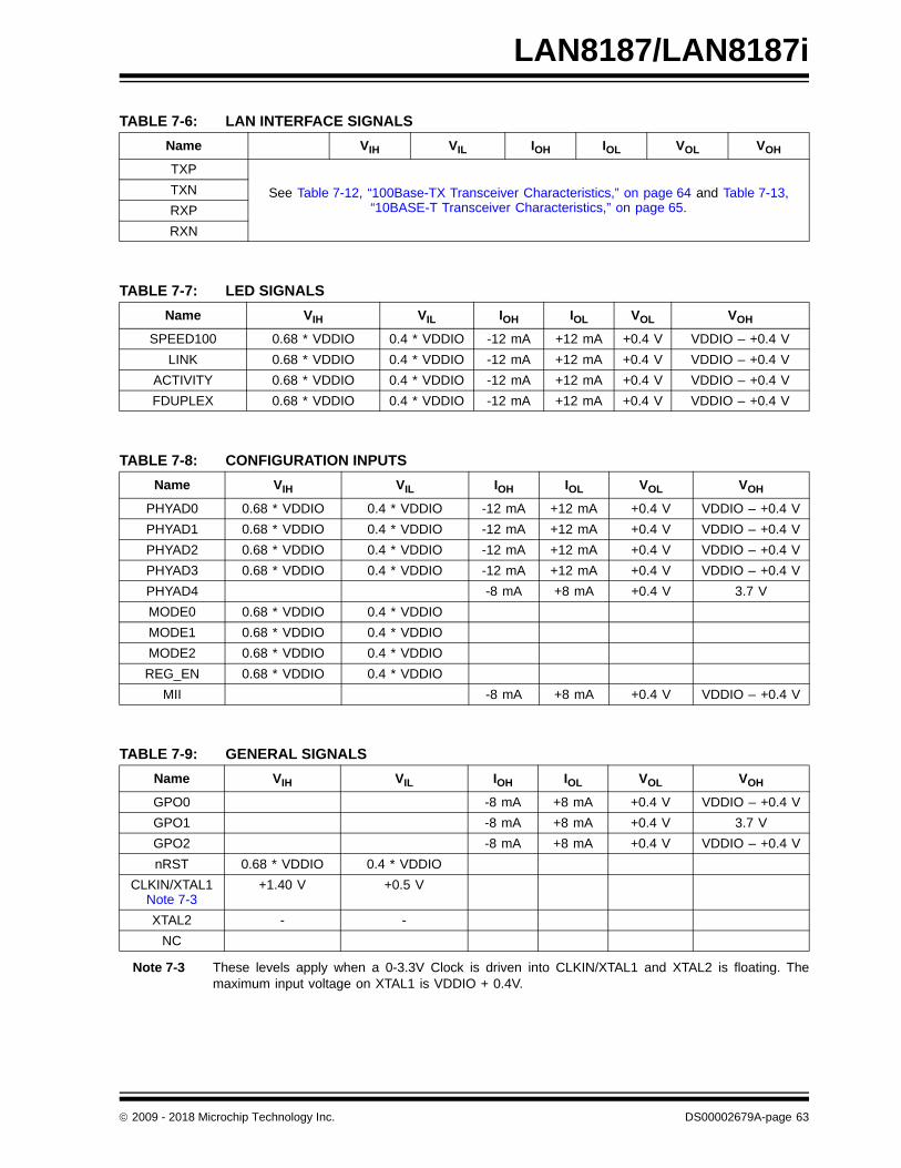
LAN8187/LAN8187i
Note 7-3 These levels apply when a 0-3.3V Clock is driven into CLKIN/XTAL1 and XTAL2 is floating. Themaximum input voltage on XTAL1 is VDDIO + 0.4V.
TABLE 7-6: LAN INTERFACE SIGNALS
Name VIH VIL IOH IOL VOL VOH
TXP
See Table 7-12, “100Base-TX Transceiver Characteristics,” on page 64 and Table 7-13, “10BASE-T Transceiver Characteristics,” on page 65.
TXN
RXP
RXN
TABLE 7-7: LED SIGNALS
Name VIH VIL IOH IOL VOL VOH
SPEED100 0.68 * VDDIO 0.4 * VDDIO -12 mA +12 mA +0.4 V VDDIO – +0.4 V
LINK 0.68 * VDDIO 0.4 * VDDIO -12 mA +12 mA +0.4 V VDDIO – +0.4 V
ACTIVITY 0.68 * VDDIO 0.4 * VDDIO -12 mA +12 mA +0.4 V VDDIO – +0.4 V
FDUPLEX 0.68 * VDDIO 0.4 * VDDIO -12 mA +12 mA +0.4 V VDDIO – +0.4 V
TABLE 7-8: CONFIGURATION INPUTS
Name VIH VIL IOH IOL VOL VOH
PHYAD0 0.68 * VDDIO 0.4 * VDDIO -12 mA +12 mA +0.4 V VDDIO – +0.4 V
PHYAD1 0.68 * VDDIO 0.4 * VDDIO -12 mA +12 mA +0.4 V VDDIO – +0.4 V
PHYAD2 0.68 * VDDIO 0.4 * VDDIO -12 mA +12 mA +0.4 V VDDIO – +0.4 V
PHYAD3 0.68 * VDDIO 0.4 * VDDIO -12 mA +12 mA +0.4 V VDDIO – +0.4 V
PHYAD4 -8 mA +8 mA +0.4 V 3.7 V
MODE0 0.68 * VDDIO 0.4 * VDDIO
MODE1 0.68 * VDDIO 0.4 * VDDIO
MODE2 0.68 * VDDIO 0.4 * VDDIO
REG_EN 0.68 * VDDIO 0.4 * VDDIO
MII -8 mA +8 mA +0.4 V VDDIO – +0.4 V
TABLE 7-9: GENERAL SIGNALS
Name VIH VIL IOH IOL VOL VOH
GPO0 -8 mA +8 mA +0.4 V VDDIO – +0.4 V
GPO1 -8 mA +8 mA +0.4 V 3.7 V
GPO2 -8 mA +8 mA +0.4 V VDDIO – +0.4 V
nRST 0.68 * VDDIO 0.4 * VDDIO
CLKIN/XTAL1Note 7-3
+1.40 V +0.5 V
XTAL2 - -
NC
2009 - 2018 Microchip Technology Inc. DS00002679A-page 63

LAN8187/LAN8187i
Note 7-4 Measured at the line side of the transformer, line replaced by 100 (+/- 1%) resistor.
Note 7-5 Offset from 16 nS pulse width at 50% of pulse peak
Note 7-6 Measured differentially.
TABLE 7-10: ANALOG REFERENCES
Name Buffer Type VIH VIL IOH IOL VOL VOH
EXRES1 AI
NC AI/O
TABLE 7-11: INTERNAL PULL-UP / PULL-DOWN CONFIGURATIONS
Name Pull-Up or Pull-Down
SPEED100/PHYAD0 Pull-up
LINK/PHYAD1 Pull-up
ACTIVITY/PHYAD2 Pull-up
FDUPLEX//PHYAD3 Pull-up
GPO1/PHYAD4 Pull-up
MODE0 Pull-up
MODE1 Pull-up
MODE2 Pull-up
nINT/TX_ER/TXD4 Pull-up
nRST Pull-up
RXD3/nINTSEL Pull-up
MDIO Pull-down
MDC Pull-down
RX_ER/RXD4 Pull-down
RX_DV Pull-down
GPO0/RMII Pull-down
TXEN Pull-down
COL Pull-down
TABLE 7-12: 100BASE-TX TRANSCEIVER CHARACTERISTICS
Parameter Symbol MIN TYP MAX Units Notes
Peak Differential Output Voltage High VPPH 950 - 1050 mVpk Note 7-4
Peak Differential Output Voltage Low VPPL -950 - -1050 mVpk Note 7-4
Signal Amplitude Symmetry VSS 98 - 102 % Note 7-4
Signal Rise & Fall Time TRF 3.0 - 5.0 nS Note 7-4
Rise & Fall Time Symmetry TRFS - - 0.5 nS Note 7-4
Duty Cycle Distortion DCD 35 50 65 % Note 7-5
Overshoot & Undershoot VOS - - 5 %
Jitter 1.4 nS Note 7-6
DS00002679A-page 64 2009 - 2018 Microchip Technology Inc.

LAN8187/LAN8187i
Note 7-7 Min/max voltages provided as measured with 100 resistive load.
TABLE 7-13: 10BASE-T TRANSCEIVER CHARACTERISTICS
Parameter Symbol MIN TYP MAX Units Notes
Transmitter Peak Differential Output Voltage VOUT 2.2 2.5 2.8 V Note 7-7
Receiver Differential Squelch Threshold VDS 300 420 585 mV
2009 - 2018 Microchip Technology Inc. DS00002679A-page 65

LAN8187/LAN8187i
DS00002679A-page 66 2009 - 2018 Microchip Technology Inc.
8.0 APPLICATION NOTES
8.1 Magnetics Selection
For a list of magnetics selected to operate with the Microchip LAN8187, please refer to the Application note “AN 8-13Suggested Magnetics”.
http://ww1.microchip.com/downloads/en/AppNotes/en562793.pdf
8.2 Application Notes
Application examples are given in pdf format on the Microchip LAN8187 web site. The link to the web site is shownbelow.
http://www.microchip.com/search/searchapp/searchhome.aspx?q=lan8187
Please check the web site periodically for the latest updates.
8.3 Reference Designs
The LAN8187 Reference designs are available on the Microchip LAN8187 web site link below.
http://www.microchip.com/search/searchapp/searchhome.aspx?q=lan8187
The reference designs are available in four variations:
a) MII with +3.3V IO
b) RMII with +3.3V IO
c) MII with +1.8V IO
d) RMII with +1.8V IO.
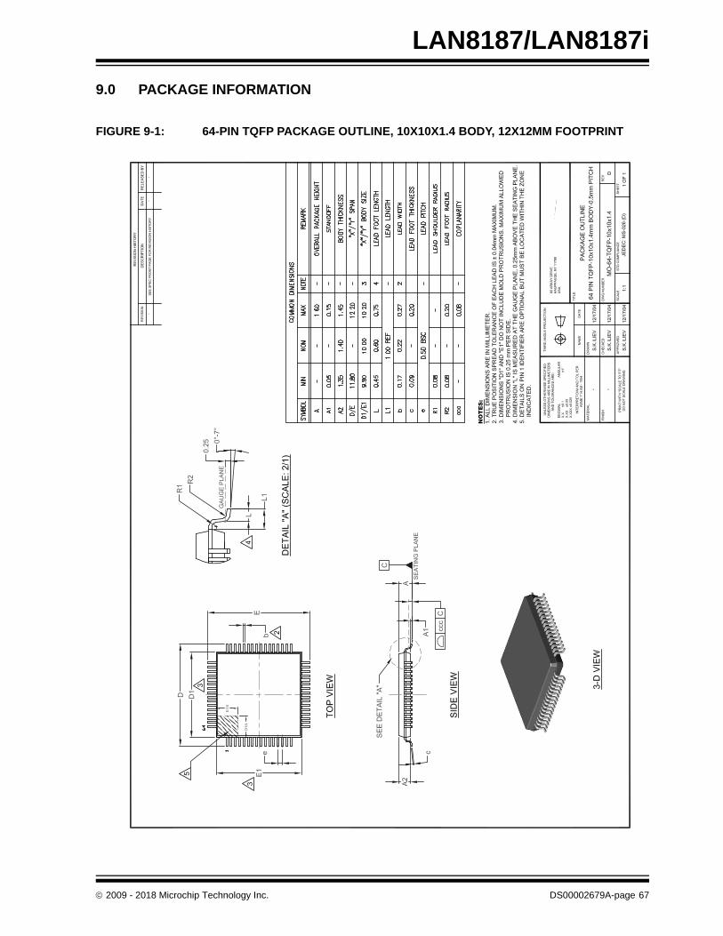
2009 - 2018 Microchip Technology Inc. DS00002679A-page 67
LAN8187/LAN8187i
9.0 PACKAGE INFORMATION
FIGURE 9-1: 64-PIN TQFP PACKAGE OUTLINE, 10X10X1.4 BODY, 12X12MM FOOTPRINT

LAN8187/LAN8187i
APPENDIX A: DATA SHEET REVISION HISTORY
TABLE A-1: REVISION HISTORY
Revision Level & Date Section/Figure/Entry Correction
DS00002679A (03-27-18) REV A replaces previous SMSC version 1.7 (03-04-11)
Product Identification Sys-tem on page 71
Removed tape & reel information
Cover Document title modified: “+15kV ESD Protected” removed.
The following bullets removed:10/100 PCMCIA/CardBus Applications, Automotive Networking”
Section 1.0, "General Description"
“Analog Interface IC” changed to “Ethernet Trans-ceiver”.
Section 1.1, "Architectural Overview" modified.
Section 8.4, “Evaluation Board”
Section removed as EVB no longer available.
Rev. 1.7 (03-04-11) Table 6-1, “SMI Timing Val-ues,” on page 48
Corrected T1.2 maximum value to 300ns.
Table 6-11, “Reset Timing Values,” on page 57
Corrected T11.4 minimum value to 3ns.
Corrected T11.3 to 2ns.
Table 7-5, “MII Bus Interface Signals,” on page 62,
Table 7-7, “LED Signals,” on page 63, Table 7-8, “Config-uration Inputs,” on page 63,
Table 7-9, “General Sig-nals,” on page 63
Corrected VIH and VIL values to 0.68*VDDIO and 0.4*VDDIO, respectively.
Table 5-39, “Register 18 - Special Modes,” on page 38
Corrected errrant bit 15 description (reserved).
Updated MIIMODE bit description and added note: “When writing to this register, the default value of this bit must always be written back.”
Added note regarding default MIIMODE value.
Section 4.6.3, "MII vs. RMII Configuration," on page 21
Updated section to remove information about regis-ter control of the MII/RMII mode.
Section 5.4.8.2, "Far Loop-back," on page 45
Updated section to remove information about regis-ter control of the MII/RMII mode.
DS00002679A-page 68 2009 - 2018 Microchip Technology Inc.

LAN8187/LAN8187i
Rev. 1.6 (02-27-09) Section 4.6.3, "MII vs. RMII Configuration"
Revised the first two paragraphs.
Table 6-11, "Reset Timing Values"
Changed the MIN value for T11.3:From: “400”To: “10”
Section 6.6, "Clock Circuit" Added section on clock, with crystal specification table.
Section 6.3, "RMII 10/100Base-TX/RX Timings"
Improved timing values.
Section 5.4.6, "Reset" Removed reference to internal POR system. Added note that the nRST should be low until VDDIO and VDD_CORE are stable. Added Figure.
Table 5-34, "Register 4 - Auto Negotiation Advertise-
ment"
Corrected bit value for Asymmetric and Symmetric PAUSE.
Section 5.4.8, "Loopback Operation"
Enhanced this section.
Section 4.6.3, "MII vs. RMII Configuration"
Added information about register bit 18.14.
Section 4.6.2.1, "Reference Clock"
First sentence of second paragraph changed:From: “between 35% and 65%”To: “between 40% and 60%“
TABLE A-1: REVISION HISTORY
Revision Level & Date Section/Figure/Entry Correction
2009 - 2018 Microchip Technology Inc. DS00002679A-page 69
LAN8187/LAN8187i
DS00002679A-page 70 2009 - 2018 Microchip Technology Inc.
THE MICROCHIP WEB SITE
Microchip provides online support via our WWW site at www.microchip.com. This web site is used as a means to makefiles and information easily available to customers. Accessible by using your favorite Internet browser, the web site con-tains the following information:
• Product Support – Data sheets and errata, application notes and sample programs, design resources, user’s guides and hardware support documents, latest software releases and archived software
• General Technical Support – Frequently Asked Questions (FAQ), technical support requests, online discussion groups, Microchip consultant program member listing
• Business of Microchip – Product selector and ordering guides, latest Microchip press releases, listing of semi-nars and events, listings of Microchip sales offices, distributors and factory representatives
CUSTOMER CHANGE NOTIFICATION SERVICE
Microchip’s customer notification service helps keep customers current on Microchip products. Subscribers will receivee-mail notification whenever there are changes, updates, revisions or errata related to a specified product family ordevelopment tool of interest.
To register, access the Microchip web site at www.microchip.com. Under “Support”, click on “Customer Change Notifi-cation” and follow the registration instructions.
CUSTOMER SUPPORT
Users of Microchip products can receive assistance through several channels:
• Distributor or Representative
• Local Sales Office
• Field Application Engineer (FAE)
• Technical Support
Customers should contact their distributor, representative or field application engineer (FAE) for support. Local salesoffices are also available to help customers. A listing of sales offices and locations is included in the back of this docu-ment.
Technical support is available through the web site at: http://www.microchip.com/support

2009 - 2018 Microchip Technology Inc. DS00002679A-page 71
LAN8187/LAN8187i
PRODUCT IDENTIFICATION SYSTEM
To order or obtain information, e.g., on pricing or delivery, refer to the factory or the listed sales office.
Device: LAN8187, LAN8187i
Temperature Range:
Blank = 0C to +70C (Commercial)i = -40C to +85C (Industrial)
Package: JT = 64-pin TQFP
Examples:
a) LAN8187-JTCommercial Temperature64-pin TQFP RoHS Compliant PackageTray
b) LAN8187i-JTIndustrial Temperature64-pin TQFP RoHS Compliant PackageTray
PART NO. [X] XX
PackageTemperatureRange
Device
-

LAN8187/LAN8187i
DS
Note the following details of the code protection feature on Microchip devices:
• Microchip products meet the specification contained in their particular Microchip Data Sheet.
• Microchip believes that its family of products is one of the most secure families of its kind on the market today, when used in the intended manner and under normal conditions.
• There are dishonest and possibly illegal methods used to breach the code protection feature. All of these methods, to our knowledge, require using the Microchip products in a manner outside the operating specifications contained in Microchip’s Data Sheets. Most likely, the person doing so is engaged in theft of intellectual property.
• Microchip is willing to work with the customer who is concerned about the integrity of their code.
• Neither Microchip nor any other semiconductor manufacturer can guarantee the security of their code. Code protection does not mean that we are guaranteeing the product as “unbreakable.”
Code protection is constantly evolving. We at Microchip are committed to continuously improving the code protection features of ourproducts. Attempts to break Microchip’s code protection feature may be a violation of the Digital Millennium Copyright Act. If such actsallow unauthorized access to your software or other copyrighted work, you may have a right to sue for relief under that Act.
Information contained in this publication regarding device applications and the like is provided only for your convenience and may besuperseded by updates. It is your responsibility to ensure that your application meets with your specifications. MICROCHIP MAKES NOREPRESENTATIONS OR WARRANTIES OF ANY KIND WHETHER EXPRESS OR IMPLIED, WRITTEN OR ORAL, STATUTORY OROTHERWISE, RELATED TO THE INFORMATION, INCLUDING BUT NOT LIMITED TO ITS CONDITION, QUALITY, PERFORMANCE,MERCHANTABILITY OR FITNESS FOR PURPOSE. Microchip disclaims all liability arising from this information and its use. Use of Micro-chip devices in life support and/or safety applications is entirely at the buyer’s risk, and the buyer agrees to defend, indemnify and holdharmless Microchip from any and all damages, claims, suits, or expenses resulting from such use. No licenses are conveyed, implicitly orotherwise, under any Microchip intellectual property rights unless otherwise stated.
Trademarks
The Microchip name and logo, the Microchip logo, AnyRate, AVR, AVR logo, AVR Freaks, BeaconThings, BitCloud, CryptoMemory, CryptoRF, dsPIC, FlashFlex, flexPWR, Heldo, JukeBlox, KEELOQ, KEELOQ logo, Kleer, LANCheck, LINK MD, maXStylus, maXTouch, MediaLB, megaAVR, MOST, MOST logo, MPLAB, OptoLyzer, PIC, picoPower, PICSTART, PIC32 logo, Prochip Designer, QTouch, RightTouch, SAM-BA, SpyNIC, SST, SST Logo, SuperFlash, tinyAVR, UNI/O, and XMEGA are registered trademarks of Microchip Technology Incorporated in the U.S.A. and other countries.
ClockWorks, The Embedded Control Solutions Company, EtherSynch, Hyper Speed Control, HyperLight Load, IntelliMOS, mTouch, Precision Edge, and Quiet-Wire are registered trademarks of Microchip Technology Incorporated in the U.S.A.
Adjacent Key Suppression, AKS, Analog-for-the-Digital Age, Any Capacitor, AnyIn, AnyOut, BodyCom, chipKIT, chipKIT logo, CodeGuard, CryptoAuthentication, CryptoCompanion, CryptoController, dsPICDEM, dsPICDEM.net, Dynamic Average Matching, DAM, ECAN, EtherGREEN, In-Circuit Serial Programming, ICSP, Inter-Chip Connectivity, JitterBlocker, KleerNet, KleerNet logo, Mindi, MiWi, motorBench, MPASM, MPF, MPLAB Certified logo, MPLIB, MPLINK, MultiTRAK, NetDetach, Omniscient Code Generation, PICDEM, PICDEM.net, PICkit, PICtail, PureSilicon, QMatrix, RightTouch logo, REAL ICE, Ripple Blocker, SAM-ICE, Serial Quad I/O, SMART-I.S., SQI, SuperSwitcher, SuperSwitcher II, Total Endurance, TSHARC, USBCheck, VariSense, ViewSpan, WiperLock, Wireless DNA, and ZENA are trademarks of Microchip Technology Incorporated in the U.S.A. and other countries.
SQTP is a service mark of Microchip Technology Incorporated in the U.S.A.
Silicon Storage Technology is a registered trademark of Microchip Technology Inc. in other countries.
GestIC is a registered trademark of Microchip Technology Germany II GmbH & Co. KG, a subsidiary of Microchip Technology Inc., in other countries.
All other trademarks mentioned herein are property of their respective companies.
© 2009 - 2018, Microchip Technology Incorporated, All Rights Reserved.
ISBN: 9781522428015
00002679A-page 72 2009 - 2018 Microchip Technology Inc.
Microchip received ISO/TS-16949:2009 certification for its worldwide headquarters, design and wafer fabrication facilities in Chandler and Tempe, Arizona; Gresham, Oregon and design centers in California and India. The Company’s quality system processes and procedures are for its PIC® MCUs and dsPIC® DSCs, KEELOQ® code hopping devices, Serial EEPROMs, microperipherals, nonvolatile memory and analog products. In addition, Microchip’s quality system for the design and manufacture of development systems is ISO 9001:2000 certified.
QUALITYMANAGEMENTSYSTEMCERTIFIEDBYDNV
== ISO/TS16949==

2009 - 2018 Microchip Technology Inc. DS00002679A-page 73
AMERICASCorporate Office2355 West Chandler Blvd.Chandler, AZ 85224-6199Tel: 480-792-7200 Fax: 480-792-7277Technical Support: http://www.microchip.com/supportWeb Address: www.microchip.com
AtlantaDuluth, GA Tel: 678-957-9614 Fax: 678-957-1455
Austin, TXTel: 512-257-3370
BostonWestborough, MA Tel: 774-760-0087 Fax: 774-760-0088
ChicagoItasca, IL Tel: 630-285-0071 Fax: 630-285-0075
DallasAddison, TX Tel: 972-818-7423 Fax: 972-818-2924
DetroitNovi, MI Tel: 248-848-4000
Houston, TX Tel: 281-894-5983
IndianapolisNoblesville, IN Tel: 317-773-8323Fax: 317-773-5453Tel: 317-536-2380
Los AngelesMission Viejo, CA Tel: 949-462-9523Fax: 949-462-9608Tel: 951-273-7800
Raleigh, NC Tel: 919-844-7510
New York, NY Tel: 631-435-6000
San Jose, CA Tel: 408-735-9110Tel: 408-436-4270
Canada - TorontoTel: 905-695-1980 Fax: 905-695-2078
ASIA/PACIFICAustralia - SydneyTel: 61-2-9868-6733
China - BeijingTel: 86-10-8569-7000
China - ChengduTel: 86-28-8665-5511
China - ChongqingTel: 86-23-8980-9588
China - DongguanTel: 86-769-8702-9880
China - GuangzhouTel: 86-20-8755-8029
China - HangzhouTel: 86-571-8792-8115
China - Hong Kong SARTel: 852-2943-5100
China - NanjingTel: 86-25-8473-2460
China - QingdaoTel: 86-532-8502-7355
China - ShanghaiTel: 86-21-3326-8000
China - ShenyangTel: 86-24-2334-2829
China - ShenzhenTel: 86-755-8864-2200
China - SuzhouTel: 86-186-6233-1526
China - WuhanTel: 86-27-5980-5300
China - XianTel: 86-29-8833-7252
China - XiamenTel: 86-592-2388138
China - ZhuhaiTel: 86-756-3210040
ASIA/PACIFICIndia - BangaloreTel: 91-80-3090-4444
India - New DelhiTel: 91-11-4160-8631
India - PuneTel: 91-20-4121-0141
Japan - OsakaTel: 81-6-6152-7160
Japan - TokyoTel: 81-3-6880- 3770
Korea - DaeguTel: 82-53-744-4301
Korea - SeoulTel: 82-2-554-7200
Malaysia - Kuala LumpurTel: 60-3-7651-7906
Malaysia - PenangTel: 60-4-227-8870
Philippines - ManilaTel: 63-2-634-9065
SingaporeTel: 65-6334-8870
Taiwan - Hsin ChuTel: 886-3-577-8366
Taiwan - KaohsiungTel: 886-7-213-7830
Taiwan - TaipeiTel: 886-2-2508-8600
Thailand - BangkokTel: 66-2-694-1351
Vietnam - Ho Chi MinhTel: 84-28-5448-2100
EUROPEAustria - WelsTel: 43-7242-2244-39Fax: 43-7242-2244-393
Denmark - CopenhagenTel: 45-4450-2828 Fax: 45-4485-2829
Finland - EspooTel: 358-9-4520-820
France - ParisTel: 33-1-69-53-63-20 Fax: 33-1-69-30-90-79
Germany - GarchingTel: 49-8931-9700
Germany - HaanTel: 49-2129-3766400
Germany - HeilbronnTel: 49-7131-67-3636
Germany - KarlsruheTel: 49-721-625370
Germany - MunichTel: 49-89-627-144-0 Fax: 49-89-627-144-44
Germany - RosenheimTel: 49-8031-354-560
Israel - Ra’anana Tel: 972-9-744-7705
Italy - Milan Tel: 39-0331-742611 Fax: 39-0331-466781
Italy - PadovaTel: 39-049-7625286
Netherlands - DrunenTel: 31-416-690399 Fax: 31-416-690340
Norway - TrondheimTel: 47-7289-7561
Poland - WarsawTel: 48-22-3325737
Romania - BucharestTel: 40-21-407-87-50
Spain - MadridTel: 34-91-708-08-90Fax: 34-91-708-08-91
Sweden - GothenbergTel: 46-31-704-60-40
Sweden - StockholmTel: 46-8-5090-4654
UK - WokinghamTel: 44-118-921-5800Fax: 44-118-921-5820
Worldwide Sales and Service
10/25/17