large area flat panel photon counting imaging … · large area flat panel photon counting imaging...
TRANSCRIPT

Large Area Flat Panel Photon Counting Imaging Detectors for Astronomy and Night Time Sensing
Oswald H. W. Siegmund, Jason B. McPhate, Anton S. Tremsin, John V. Vallerga
Space Sciences Laboratory, U.C. Berkeley Henry Frisch
University of Chicago Robert Wagner, Anil Mane, Jeffrey Elam Argonne National Laboratory, Chicago Il
Gary Varner University of Hawaii
ABSTRACT
The development of large area, high performance, photon counting, imaging, timing detectors based on novel
microchannel plate technology potentially offers significant advantages in a number of applications. To explore this, large area (20 cm) microchannel plates have been constructed using borosilicate microcapillary arrays (20 µm pores) activated by atomic layer deposition. These microchannel plates have demonstrated gain equivalent to conventional microchannel plates, have low background rates (0.07 events cm-2 sec-1), good gain uniformity (10%) and very good lifetime stability (to 7 C cm-2) when using appropriate secondary emissive coatings. Tests with various readout schemes have been done, achieving high thoughput rates of up to 5 MHz and spatial resolution sufficient to resolve individual 20 µm pores. A full process run has been accomplished with a 20 cm format sealed tube configuration. This included deposition of a 20 cm bialkali photocathode with peak quantum efficiency of ~25% at 350 nm, good stability and ±15% uniformity over the active area. Post process testing demonstrates event time determination better than 200 ps FWHM.
Keywords: Photon counting, imaging, timing, microchannel plate
1. INTRODUCTION
The development of large area, high performance, photon counting, imaging, timing detectors has significance for “open faced” configurations for UV and particle detection in space astrophysics, mass spectroscopy and many time-of–flight applications. Furthermore, sealed tube configurations for optical/UV sensing also have applications in detection of Cherenkov light (RICH), scintillation detection, neutron imaging applications, astronomy, night time remote reconnaissance, airborne/space situational awareness, and homeland security. Commercially available devices are generally smaller than 5 cm and do not have high spatial resolution. A collaboration consisting of the U. Chicago, Argonne National Laboratory, U.C. Berkeley, U. Hawaii and other institutions have developed novel technologies to realize 20 cm format open face (NASA) or sealed tube detectors (Large Area Picosecond Photon Detector) to deliver performance characteristics as good, or better, than existing smaller devices.
A depiction of a microchannel plate (MCP) detector scheme is shown in Fig. 1. In this “sealed tube” device the radiation passes through the input window and is converted to photoelectrons by a photocathode. The emitted photoelectrons are amplified by a pair of MCPs and are then detected by a readout anode that is a series of conductive strips, in one, or both X and Y directions. We have used these devices as photon counting, imaging, event time tagging detector schemes for a number of astronomical [1-6], remote sensing [7], time resolved biological imaging [8, 9], photoelectron emission spectroscopy [10] and night time sensing [11] applications. Achieving a detector area of 20 x 20 cm is potentially problematic because MCPs of this size are not typically available, and in such sizes would be costly and less robust. The development of MCPs using borosilicate micro-capillary arrays [12] with pore sizes of 20 µm, functionalized with resistive and photoemissive layers by atomic layer deposition (ALD) potentially solves these issues. These ALD borosilicate MCPs have been tested, mainly in 33mm format, and provide many performance characteristics typical of conventional microchannel plates [12]. We have also assessed ALD MCPs up to 20 cm format. ALD MCPs have shown low intrinsic background [13] (<0.07 events cm-2 s-1), low outgassing during preconditioning vacuum bake [13], and virtually no gain degradation over at least 7 C cm-2 of charge extraction [13]. Tests described here, in large detectors with cross strip, and cross delay line readouts have achieved better than 25µm imaging resolution (FWHM), good gain uniformity, event timing <200ps and >5 MHz event rates. Alongside this effort we have made stable, uniform 20 cm bialkali photocathodes with >20% quantum efficiency on borosilicate windows compatible with construction of the large sealed tube devices. Subsequently, we have begun to construct a fully
functional sealed tube design device with ALD MCPs, and a bialkali photocathode, and have tested a complete device inside a vacuum tube processing chamber. Once completed, a 20cm sealed tube detector will provide a significant new tool for astronomy, night time remote reconnaissance, airborne/space situational awareness and other applications requiring large area photodetectors such as Cherenkov (RICH) imaging.
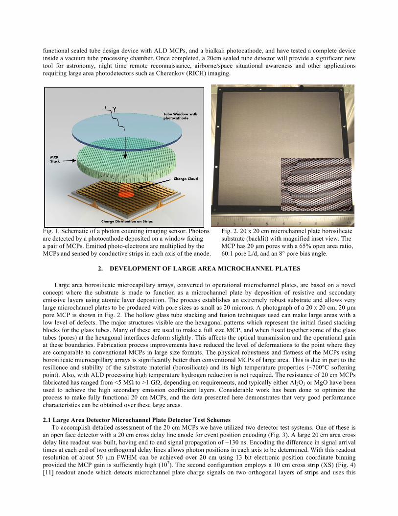
Fig. 1. Schematic of a photon counting imaging sensor. Photons Fig. 2. 20 x 20 cm microchannel plate borosilicate are detected by a photocathode deposited on a window facing substrate (backlit) with magnified inset view. The a pair of MCPs. Emitted photo-electrons are multiplied by the MCP has 20 µm pores with a 65% open area ratio, MCPs and sensed by conductive strips in each axis of the anode. 60:1 pore L/d, and an 8° pore bias angle.
2. DEVELOPMENT OF LARGE AREA MICROCHANNEL PLATES
Large area borosilicate microcapillary arrays, converted to operational microchannel plates, are based on a novel concept where the substrate is made to function as a microchannel plate by deposition of resistive and secondary emissive layers using atomic layer deposition. The process establishes an extremely robust substrate and allows very large microchannel plates to be produced with pore sizes as small as 20 microns. A photograph of a 20 x 20 cm, 20 µm pore MCP is shown in Fig. 2. The hollow glass tube stacking and fusion techniques used can make large areas with a low level of defects. The major structures visible are the hexagonal patterns which represent the initial fused stacking blocks for the glass tubes. Many of these are used to make a full size MCP, and when fused together some of the glass tubes (pores) at the hexagonal interfaces deform slightly. This affects the optical transmission and the operational gain at these boundaries. Fabrication process improvements have reduced the level of deformations to the point where they are comparable to conventional MCPs in large size formats. The physical robustness and flatness of the MCPs using borosilicate microcapillary arrays is significantly better than conventional MCPs of large area. This is due in part to the resilience and stability of the substrate material (borosilicate) and its high temperature properties (~700°C softening point). Also, with ALD processing high temperature hydrogen reduction is not required. The resistance of 20 cm MCPs fabricated has ranged from <5 MΩ to >1 GΩ, depending on requirements, and typically either Al2O3 or MgO have been used to achieve the high secondary emission coefficient layers. Considerable work has been done to optimize the process to make fully functional 20 cm MCPs, and the data presented here demonstrates that very good performance characteristics can be obtained over these large areas. 2.1 Large Area Detector Microchannel Plate Detector Test Schemes
To accomplish detailed assessment of the 20 cm MCPs we have utilized two detector test systems. One of these is an open face detector with a 20 cm cross delay line anode for event position encoding (Fig. 3). A large 20 cm area cross delay line readout was built, having end to end signal propagation of ~130 ns. Encoding the difference in signal arrival times at each end of two orthogonal delay lines allows photon positions in each axis to be determined. With this readout resolution of about 50 µm FWHM can be achieved over 20 cm using 13 bit electronic position coordinate binning provided the MCP gain is sufficiently high (107). The second configuration employs a 10 cm cross strip (XS) (Fig. 4) [11] readout anode which detects microchannel plate charge signals on two orthogonal layers of strips and uses this

charge division and centroiding of the charge distribution to encode event X-Y positions, and event times. The cross strip readout has very high spatial resolution (<25 µm FWHM) at relatively low gain (1 x 10⁶) and can be used to see detailed image features. Both detector schemes provide event by event accumulated images and gain map images for the MCPs that can be used to characterize the efficiency, overall uniformity, background rate and spatial resolution of the 20 cm ALD MCPs when used in a pair configuration (Fig. 1).
Fig. 3: 20 cm cross delay line readout detector (with MCPs Fig. 4: Front face of a 10 cm cross strip readout detector installed) used for tests and imaging of 20 cm ALD MCPs. used for high rate/resolution testing of ALD MCPs. 2.2 Imaging Tests with Large Area Atomic Layer Deposited Microchannel Plates
Tests with 33mm format ALD MCPs on borosilicate substrates have established that the gain, pulse amplitude distribution, and MCP resistance are similar to conventional MCPs [12]. The background rate (~0.07 events cm-2 sec-1, [13]) is 2 to 4 times lower than conventional MCPs because the borosilicate glass has less radioactive beta decay from potassium or rubidium than conventional MCP glass compositions. We have also performed preconditioning steps (bake, burn-in) on 33mm borosilicate ALD microchannel plates [12]. This shows that vacuum baking or burn-in causes an asymptotic gain increase for MgO coated ALD MCPs, which can then remain stable for up to 7 C cm-2 at gains of ~106 [14].
Similar tests on 20 cm MCPs have been initiated, where the standard format is 20cm, pore size of 20 µm, 60:1 L/d with 8° pore bias angle. The gains we have achieved with the 20 cm ALD MCP pairs can reach 107 or greater. However, with a 0.75mm inter-MCP gap and 200 V bias applied we routinely obtain ~ 5 x 10⁶ gain, with a peaked pulse amplitude distribution [15], using ~1000 v applied to each MCP. This is essentially the same as the results for the 33 mm MCPs. However, with the large area format the problems expected were potential issues with the uniformity of the operating characteristics. This was confirmed with early devices [13], but since then considerable improvements have been made. One example is the gain uniformity over a 20 cm MCP pair. A gain map image containing 3 x 10⁸ events (Fig. 5) shows that the gain uniformity over the entire area is better than 10% (Fig. 6). Mottling of the gain map image in Fig. 5 is due to the small gain variations for individual MCP hexagonal multifibers, in common with conventional MCPs. Such a small degree of gain variation promotes better performance characteristics for overall image resolution and detection efficiency.
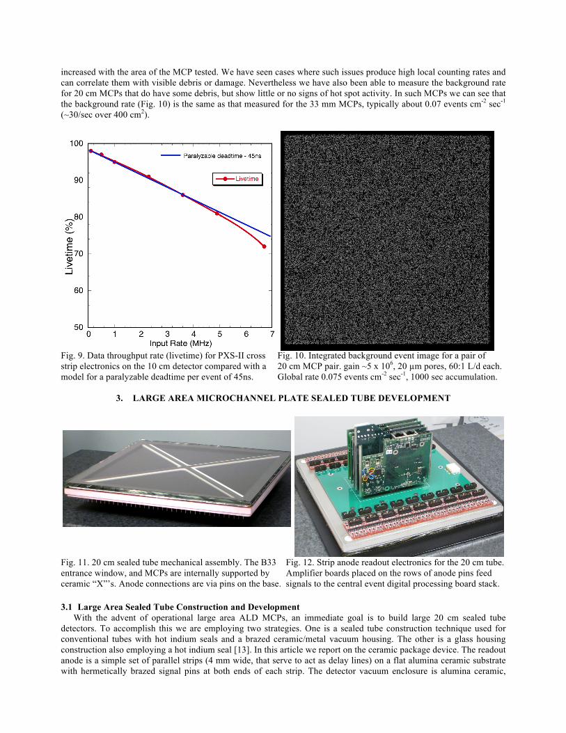
Image quality tests using the 20 cm detector with a cross delay line readout (Fig. 7) at 4k x 4k pixel binning show an overall pattern of striations. This is uniquely due to the cross delay line anode structure used for these tests. Examination of the image at higher magnification shows the effect of the MCP pore stacking structure (hexagonal multifiber) is clearly visible as dark or bright hexagonal edge modulation. Such images can be routinely accumulated at event rates of up to ~1 MHz, and provide useful information on individual MCP ALD processing. More detailed imaging can be achieved over 10 cm areas using the cross strip readout detector. High resolution images of the MCP structure using this system at relatively low gain (2 x 10⁶) reveals (Fig. 8) the image modulation at the hexagonal boundaries and can actually resolve the 20 µm MCP pores in much of the image. To obtain the statistics to achieve this imaging fidelity the cross strip system has the capability of processing events at high rates. The throughput of the PXS-II electronics is primarily limited by the multichannel input amplifier time constant, since the subsequent ADC’s and FPGA position processing algorithms are both faster and digitally pipelined. Throughput tests (Fig. 9) measured comparing the input count rate with the output rate of processed events fits a model with ~45ns dead time. This is close

to expectations, and allows images to be accumulated rapidly over large areas to obtain the statistics necessary for high resolution assessments.
Fig. 5. Gain map “image” showing average gain over a 20 Fig. 6. X and Y gain histograms for Fig. 7, showing that cm MCP pair. Gain ~5 x 10⁶, 20 µm pores, 60:1 L/d each. the gain is globally uniform to the 10% level.
Fig. 7. Uniformly illuminated (184 nm) integrated image for a Fig. 8. Small section of a 20 cm MCP imaged with 20 cm MCP pair. gain ~5 x 10⁶, 20 µm pores, 60:1 L/d each. a 10 cm cross strip detector (Fig. 6). Gain ~2 x 10⁶, Striations are a delay line anode artifacts. Zoomed inset shows 20 µm pores, 60:1 L/d. Spatial resolution is high the hexagonal multifiber structure of the MCPs is visible. enough to resolve the pores in much of the area.
The background rate for borosilicate ALD MCPs is low compared to conventional MCPs as a result of low intrinsic radioactivity in the glass. This is relatively easy to establish with small MCPs, but not so with large areas. In large size formats the incidence of particulates and surface damage causing local field emission (hot spots) is proportionally
!"#$%&'()*+"
,"#$%&'()*+"
increased with the area of the MCP tested. We have seen cases where such issues produce high local counting rates and can correlate them with visible debris or damage. Nevertheless we have also been able to measure the background rate for 20 cm MCPs that do have some debris, but show little or no signs of hot spot activity. In such MCPs we can see that the background rate (Fig. 10) is the same as that measured for the 33 mm MCPs, typically about 0.07 events cm-2 sec-1
(~30/sec over 400 cm2).
Fig. 9. Data throughput rate (livetime) for PXS-II cross Fig. 10. Integrated background event image for a pair of strip electronics on the 10 cm detector compared with a 20 cm MCP pair. gain ~5 x 10⁶, 20 µm pores, 60:1 L/d each. model for a paralyzable deadtime per event of 45ns. Global rate 0.075 events cm-2 sec-1, 1000 sec accumulation.
3. LARGE AREA MICROCHANNEL PLATE SEALED TUBE DEVELOPMENT
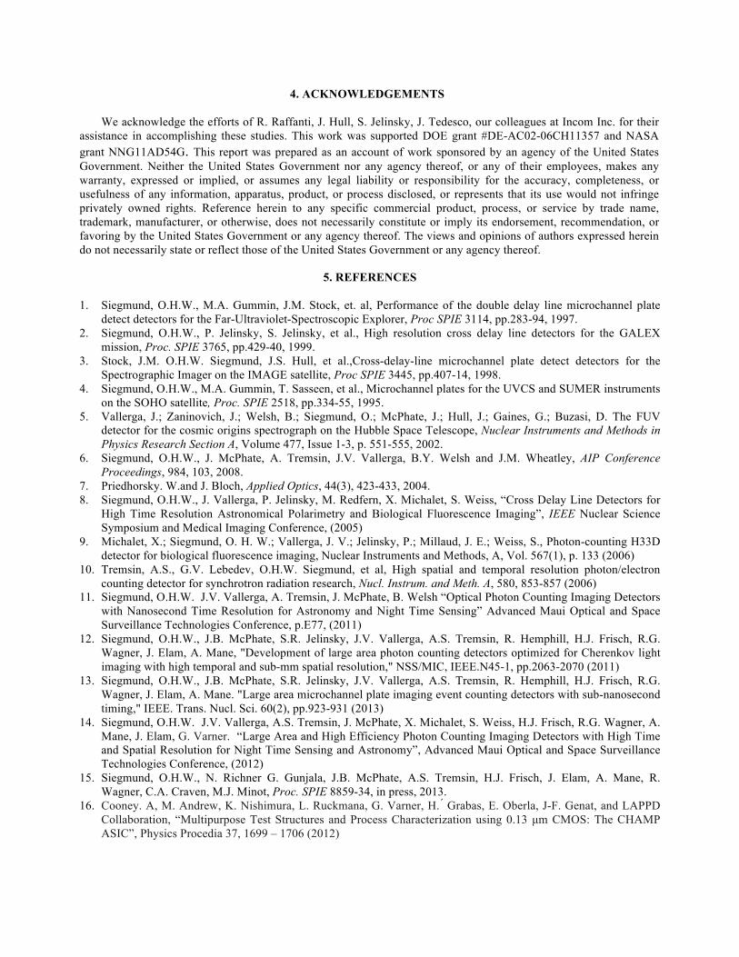
Fig. 11. 20 cm sealed tube mechanical assembly. The B33 Fig. 12. Strip anode readout electronics for the 20 cm tube. entrance window, and MCPs are internally supported by Amplifier boards placed on the rows of anode pins feed ceramic “X”’s. Anode connections are via pins on the base. signals to the central event digital processing board stack. 3.1 Large Area Sealed Tube Construction and Development
With the advent of operational large area ALD MCPs, an immediate goal is to build large 20 cm sealed tube detectors. To accomplish this we are employing two strategies. One is a sealed tube construction technique used for conventional tubes with hot indium seals and a brazed ceramic/metal vacuum housing. The other is a glass housing construction also employing a hot indium seal [13]. In this article we report on the ceramic package device. The readout anode is a simple set of parallel strips (4 mm wide, that serve to act as delay lines) on a flat alumina ceramic substrate with hermetically brazed signal pins at both ends of each strip. The detector vacuum enclosure is alumina ceramic,

which is brazed to the alumina anode substrate and has a copper well for a hot indium vacuum seal. The seal to the 5mm thick borofloat-33 entrance window produces a hermetic package < 15 mm thick (Fig. 11). Internally there are two MCPs to support gain of up to 5 x10⁶, and several getters to keep the vacuum pressure low. The window, MCPs and anode are supported by an “X” shaped set of ceramic spacers keeping the window and anode deflections minimal. The event position and time encoding electronics (Fig. 12) was developed by the University of Hawaii [16], and consists of high speed preamplifiers for each strip end coupled to a timing circuit that determines the difference in signal arrival times. The arrival time difference provides spatial imaging along each strip and allows the event times of arrival to be deduced. In addition the strip at which the signal arrives gives coarse resolution in the orthogonal axis. Facilities to produce such a sealed tube are not straightforward, so a special ultra high vacuum system was designed and built to process the detectors. This accommodates the photocathode fabrication, preconditioning of the MCPs and tube subassembly, and window sealing, and provides for extensive testing modes. Our first run through of the entire process to produce a fully implemented 20 cm sealed tube has been completed and the results are detailed below. 3.2 Large Area Photocathode Development
A key part of the task to make a 20 cm detector is to produce large area photocathodes that can be integrated and sealed into the final detector package. To detect scintillation emission with relatively low cathode noise and acceptable quantum efficiency the use of semitransparent bialkali photocathodes is well established. We have made a number of 20 cm bialkali photocathodes in two different processing chambers. In these previous attempts [13, 14] we have achieved bialkali cathodes with >20% quantum efficiency and good stability on borofloat-33 windows compatible with a 20 cm sealed tube device. During the processing of the fully implemented 20 cm sealed tube we have deposited a 20 cm Na2KSb photocathode (Fig. 13) which was immediately attached to the tube housing via a hot indium seal. The peak efficiency occurs at ~350 nm and is > 20%, tapering to ~10% at 500nm. This is similar to the prior Na2KSb photocathodes which we have constructed, and after initial stabilization the photocathode remained at the same quantum efficiency during the period of testing (~ 2 weeks) (Fig. 13). The cathode uniformity was evaluated with a focused (1 cm) beam of 400 nm light. Spot quantum efficiency measurements were positioned to avoid the “X” support structures of the tube. The general uniformity shows that the quantum efficiency varies less than ±15% over the bulk of the area, with slightly larger deviation only at one corner (Fig 14).
Fig. 13: Quantum efficiency as a function of wavelength Fig. 14: Quantum efficiency uniformity (normalized) of and time for a 20 cm bialkali (Na2KSb) photocathode, the photocathode in Fig 13 as a function of position, after deposited and attached to a 20 cm MCP detector. attachment to the MCP detector. 1 cm spot beam at 400nm. 3.3 Sealed Tube Preconditioning
Prior to photocathode deposition the required steps for preconditioning the detector and chamber were accomplished. This included a high vacuum bake at ~350 °C and burn-in of the MCPs. Earlier tests to assess the behavior of borosilicate ALD MCPs to preconditioning showed the MCP gain rises by an order of magnitude after a
0
5
10
15
20
25
30
350 400 450 500 550 600 650
QE 13 days
QE 9 days
QE 3 days
Initial QE
Qua
ntum
Effi
cien
cy (%
)
Wavelength (nm)
!"##$ #"%%$
!"#&$ !"!!$
#"%&$
#"%'$
!"#($#"%)$
#"%*$!"!!$
#"&'$
#"&*$
!"#%$
!"!*$
#"%%$
#"&)$
#"&%$
#"%*$
#"&+$
#"&%$
#"&%$
!"#,$

vacuum bake [12]. Then the MCP gain stayed virtually unchanged for gains of 105 or greater (Fig. 15) during a long term “burn-in” where 7 C cm-2 was extracted. Further tests [15] have shown that this is characteristic of the MgO secondary emissive layer used for the MCPs tested. The MCPs in this detector used Al2O3 as the secondary emissive layer which does show [15] a gain drop during preconditioning. However, this drop is generally less severe than experienced with conventional MCPs and furthermore stabilization is reached at a much smaller overall charge extraction (~0.05 C cm-2) than conventional MCPs. In this preconditioning process the post bake gas evolution of the MCPs was very low and the burn-in stabilization allowed the process to be concluded at ~0.01 C cm-2.
Fig. 15: Gain at set bias voltages for a 33mm borosilicate- Fig. 16: Detected laser pulses (80 ps laser @ 610 nm) at MgO ALD MCP pair (20 µm pore, 60:1 L/d) as a function 10 kHz rate, using the 20cm detector with a pair of 20 µm of extracted charge during UV burn-in (after 350°C bake). pore ALD MCPs and the cathode in Fig. 13. The single Shows high stability for ALD MgO over 7C cm-2 lifetime. photoelectron noise is also visible. Laser ~15e- equivalent. 3.4 20 cm Detector Testing and Event Time Resolution Performance
As configured inside the vacuum processing tank the 20 cm detector with the bialkali photocathode was not able to be attached to the final electronics package. Therefore we connected alternating ends of the anode strips to form a single continuous delay line with an end to end delay of the order 35 ns. With our standard encoding electronics it was then possible to perform event centroid position determination in both the X and Y directions to the level of 34 x 50 pixels as a guide for “in process” detector testing. One disadvantage in the tank setup is that the connections are long (20 cm), unshielded, and are not 50Ω impedance. Nevertheless we were able to show that the gain uniformity was reasonably flat during and after the preconditioning steps and that the image was uniformly illuminated.
One type of evaluation test that we were also able to accomplish in this setup is the measurement of the event timing characteristics. We have previously discussed the photon event time-tagging requirements [7, 8, 9, 10] for various applications. To measure the temporal resolution, we used a pulsed diode laser (640 nm, 80 ps pulse width) and measured the jitter in the time of arrival of the MCP exit pulse compared to the laser trigger. Detected laser pulses at each end of the delay line (Fig 16) show the laser signal repetition rate of ~10 kHz, as well as the single photoelectron noise from the photocathode. A high bandwidth preamplifier (EG&G Ortec VT100-C) was coupled to the bottom of the MCP via a high voltage capacitor, and its output (Fig. 17) fed to a constant fraction discriminator and time to digital converter to compare the detected event time to the pulse source input trigger (Fig. 17). The detector pulse output width is ~8 ns which is partly due to the 20 cm detector size, but mostly due to the signal attenuation and dispersion in the available connection scheme in the vacuum tank. The first parameter tested was the dependence of the event timing accuracy on the photocathode gap potential. The gap is fairly large (1.5 mm) so that transit time spread for emitted photoelectrons dominates for small gap voltages (< 150 v). Above 150 v the asymptotic value reached is ~ 200 ps. Using the same amplitude laser pulse, and varying the gain of the detector, the timing error asymptotes above ~ 1 x 10⁷ gain (channel ~80) at the same value (~ 200 ps). However, using a higher amplitude laser pulse (~150 photoelectron equivalent) the timing error distribution narrows to ~64 ps FWHM. Since the distribution improves with pulse detection statistics and the timing electronics signal to noise is not dominating, this suggests that some optimization of the MCP
103
104
105
106
107
108
0 1 2 3 4 5 6 7 8
2000 V1750 V1450 V1300 V
Gain
Extracted Charge (C cm-2)
Laser pulses
Single photoelectron noise

and inter MCP geometry and bias are required to make improvements. The laser spot was kept to a size of <5mm, and was placed at various points on the detector field of view, producing a localized spot image within ~ 1 pixel. All locations tested produced similar timing results.
Overall the test run for a fully implemented 20 cm sealed tube has given good results. Some modifications to the configuration and process are indicated by the test results, namely to the connection scheme and MCP configuration, but the basic process to produce photocathodes seems effective and bodes well for making fully functional sensors.
Fig. 17: Laser trigger signal (lower) and detected photon Fig. 18: Jitter of the time stamp for detected laser pulses. pulses (80 ps laser @ 640 nm) at 10 kHz rate, using the 80 ps laser @ 610 nm, at 10 kHz rate 20cm detector with 20cm detector with a pair of 20 µm pore ALD MCPs a pair of 20 µm pore ALD MCPs and the cathode in Fig. and the cathode in Fig. 13. Laser ~15e- equivalent. 13. Laser ~15e- equivalent. Cathode/MCP gap ~1.5 mm.
Fig. 19: Jitter of the time stamp for detected laser pulses. Fig. 20: Time stamp error distributions for detected laser 80 ps laser @ 610 nm, at 10 kHz rate, 20cm detector with pulses (80 ps laser @ 610 nm, 10 kHz), 20cm detector a pair of 20 µm pore ALD MCPs and the cathode in Fig. with 20 µm pore ALD MCP pair and the cathode in Fig. 13. Laser ~15e- equivalent. Cathode gap ~1.5 mm, 250 v. 13. Cathode gap ~1.5 mm, 250 v. High S/N laser ~150e-.
0
100
200
300
400
500
0 50 100 150 200 250 300
FWH
M (p
s)
PC Gap Volts
0
100
200
300
400
500
600
0 20 40 60 80 100 120 140
FWH
M (p
s)
Gain (relative)0
200
400
600
800
1000
9.5 10 10.5 11
30v Gap85v Gap145v Gap257v GapHigh S/N Laser
Cou
nts
Time (ns)
212ps FWHM230ps FWHM
480ps FWHM286ps FWHM
64 ps FWHM (27 ps rms)
4. ACKNOWLEDGEMENTS
We acknowledge the efforts of R. Raffanti, J. Hull, S. Jelinsky, J. Tedesco, our colleagues at Incom Inc. for their assistance in accomplishing these studies. This work was supported DOE grant #DE-AC02-06CH11357 and NASA grant NNG11AD54G. This report was prepared as an account of work sponsored by an agency of the United States Government. Neither the United States Government nor any agency thereof, or any of their employees, makes any warranty, expressed or implied, or assumes any legal liability or responsibility for the accuracy, completeness, or usefulness of any information, apparatus, product, or process disclosed, or represents that its use would not infringe privately owned rights. Reference herein to any specific commercial product, process, or service by trade name, trademark, manufacturer, or otherwise, does not necessarily constitute or imply its endorsement, recommendation, or favoring by the United States Government or any agency thereof. The views and opinions of authors expressed herein do not necessarily state or reflect those of the United States Government or any agency thereof.
5. REFERENCES 1. Siegmund, O.H.W., M.A. Gummin, J.M. Stock, et. al, Performance of the double delay line microchannel plate
detect detectors for the Far-Ultraviolet-Spectroscopic Explorer, Proc SPIE 3114, pp.283-94, 1997. 2. Siegmund, O.H.W., P. Jelinsky, S. Jelinsky, et al., High resolution cross delay line detectors for the GALEX
mission, Proc. SPIE 3765, pp.429-40, 1999. 3. Stock, J.M. O.H.W. Siegmund, J.S. Hull, et al.,Cross-delay-line microchannel plate detect detectors for the
Spectrographic Imager on the IMAGE satellite, Proc SPIE 3445, pp.407-14, 1998. 4. Siegmund, O.H.W., M.A. Gummin, T. Sasseen, et al., Microchannel plates for the UVCS and SUMER instruments
on the SOHO satellite, Proc. SPIE 2518, pp.334-55, 1995. 5. Vallerga, J.; Zaninovich, J.; Welsh, B.; Siegmund, O.; McPhate, J.; Hull, J.; Gaines, G.; Buzasi, D. The FUV
detector for the cosmic origins spectrograph on the Hubble Space Telescope, Nuclear Instruments and Methods in Physics Research Section A, Volume 477, Issue 1-3, p. 551-555, 2002.
6. Siegmund, O.H.W., J. McPhate, A. Tremsin, J.V. Vallerga, B.Y. Welsh and J.M. Wheatley, AIP Conference Proceedings, 984, 103, 2008.
7. Priedhorsky. W.and J. Bloch, Applied Optics, 44(3), 423-433, 2004. 8. Siegmund, O.H.W., J. Vallerga, P. Jelinsky, M. Redfern, X. Michalet, S. Weiss, “Cross Delay Line Detectors for
High Time Resolution Astronomical Polarimetry and Biological Fluorescence Imaging”, IEEE Nuclear Science Symposium and Medical Imaging Conference, (2005)
9. Michalet, X.; Siegmund, O. H. W.; Vallerga, J. V.; Jelinsky, P.; Millaud, J. E.; Weiss, S., Photon-counting H33D detector for biological fluorescence imaging, Nuclear Instruments and Methods, A, Vol. 567(1), p. 133 (2006)
10. Tremsin, A.S., G.V. Lebedev, O.H.W. Siegmund, et al, High spatial and temporal resolution photon/electron counting detector for synchrotron radiation research, Nucl. Instrum. and Meth. A, 580, 853-857 (2006)
11. Siegmund, O.H.W. J.V. Vallerga, A. Tremsin, J. McPhate, B. Welsh “Optical Photon Counting Imaging Detectors with Nanosecond Time Resolution for Astronomy and Night Time Sensing” Advanced Maui Optical and Space Surveillance Technologies Conference, p.E77, (2011)
12. Siegmund, O.H.W., J.B. McPhate, S.R. Jelinsky, J.V. Vallerga, A.S. Tremsin, R. Hemphill, H.J. Frisch, R.G. Wagner, J. Elam, A. Mane, "Development of large area photon counting detectors optimized for Cherenkov light imaging with high temporal and sub-mm spatial resolution," NSS/MIC, IEEE.N45-1, pp.2063-2070 (2011)
13. Siegmund, O.H.W., J.B. McPhate, S.R. Jelinsky, J.V. Vallerga, A.S. Tremsin, R. Hemphill, H.J. Frisch, R.G. Wagner, J. Elam, A. Mane. "Large area microchannel plate imaging event counting detectors with sub-nanosecond timing," IEEE. Trans. Nucl. Sci. 60(2), pp.923-931 (2013)
14. Siegmund, O.H.W. J.V. Vallerga, A.S. Tremsin, J. McPhate, X. Michalet, S. Weiss, H.J. Frisch, R.G. Wagner, A. Mane, J. Elam, G. Varner. “Large Area and High Efficiency Photon Counting Imaging Detectors with High Time and Spatial Resolution for Night Time Sensing and Astronomy”, Advanced Maui Optical and Space Surveillance Technologies Conference, (2012)
15. Siegmund, O.H.W., N. Richner G. Gunjala, J.B. McPhate, A.S. Tremsin, H.J. Frisch, J. Elam, A. Mane, R. Wagner, C.A. Craven, M.J. Minot, Proc. SPIE 8859-34, in press, 2013.
16. Cooney. A, M. Andrew, K. Nishimura, L. Ruckmana, G. Varner, H. ́ Grabas, E. Oberla, J-F. Genat, and LAPPD Collaboration, “Multipurpose Test Structures and Process Characterization using 0.13 µm CMOS: The CHAMP ASIC”, Physics Procedia 37, 1699 – 1706 (2012)