large area zone plate exposure by fixed beam moving stage
TRANSCRIPT

Large area zone plate exposure by
fixed beam moving stage lithography
Johan Meszaros
Master of Science Thesis Biomedical and X-Ray Physics Department of Applied Physics
KTH – Royal Institute of Technology Stockholm, Sweden 2011

ii
TRITA-FYS 2011:50 Biomedical and X-Ray Physics ISSN 0280-316X KTH/Albanova ISRN KTH/FYS/--11:50--SE SE-106 09 Stockholm
This thesis summarizes the diploma work by Johan Meszaros for the Master of Science degree in Engineering Physics. The work was performed during the winter and spring of 2011 in the nanofabrication group under the supervision of Dr. Anders Holmberg at the division of Biomedical and X-Ray Physics, KTH – Royal Institute of Technology in Stockholm, Sweden. Examiner at KTH was Prof. Hans Hertz. © Johan Meszaros, September 7, 2011 Tryck: Universitetsservice US AB

iii
Abstract
In this diploma project the so-called fixed beam moving stage (FBMS) module in the Raith 150 electron beam lithography system has been evaluated for making large area zone plate exposures. The project goal, besides the evaluation of the module, has been to find an exposure recipe for exposing zone plates with diameter up to 500 µm. The zone plates fabricated with this method will be used for synchrotron and x-ray free electron laser applications.
The thesis starts with a short introduction to zone plate properties and fabrication procedures. Then the work where FBMS exposed zone plates are compared with normal write field exposures of 75 µm diameter zone plates is described. The conclusion is that for these small diameters, major problems with wobbly zones occur for the FBMS patterns. However, for larger diameters the pattern typically looks better. The final result with large area exposures are excellent zone plate patterns with 500 µm diameter and 100 nm outermost zone width. The total exposure time was 2 h 15 min. This relatively short time indicate that it will be practically possible to use the Raith system for these large area exposures.

iv

v
Contents Abstract iii
1. Introduction 1
1.1 Fresnel zone plate lens 1
2. Zone plate fabrication process 4
2.1 Electron Beam Lithography 5
2.1.1 The lithography system 5
2.1.2 Main exposure parameter settings 6
2.1.3 Creating the pattern 7
2.1.4 Working distance and write field alignment 7
2.2 Fixed Beam Moving Stage 8
3. Experiments and results 9
3.1 Sample preparation 9
3.2 Exposure and development 9
3.3 Experiments and results 10
3.3.1 Initial experiments with 75 µm diameter zone plates 11
3.3.2 Reducing the stage speed 12
3.3.3 Fbms polygonal mode 16
3.3.4 Use of another position on the sample holder 17
3.3.5 Exposure of 500 µm diameter zone plates 19
4. Conclusion and discussion 20
5. Acknowledgement 23
6. Bibliography 24
1
1. Introduction
The construction of the new synchrotron sources, such as the x-ray free electron laser, XFEL, in Hamburg and Maxlab IV in Lund have resulted in a request for large area zone plates with a diameter of at least 500 µm and a outermost zone width no larger than 100 nm. Up till now, zone plates with a diameter of 100 µm have been fabricated by the Nanofabrication group at the Biomedical and X-Ray Physics group (BIOX) at the Royal Institute of Technology in Stockholm, Sweden. However the electron beam lithography system (Raith 150) that has been used in order to fabricate those zone plates has been the limiting factor in the production of larger zone plates. Therefore a so called FBMS (Fixed Beam Moving Stage) module which would enable the fabrication of larger zone plates was installed. The focus of this diploma work has been to explore the possibilities of this FBMS module when it comes to large area zone plate fabrication. This will be presented in the following chapters. But first, in section 1.1, a short introduction to the basic concept of zone plates is given.
1.1 The Fresnel zone plate lens
The Fresnel zone plate lens is a lens that uses diffraction in order to refract the incoming beam. Figure 1 shows an illustration. As seen, it consists of alternating transparent and opaque rings where the width of each zone is decreasing with increasing radii. The different zones are placed at a distance from the centre such that the optical path length difference for a ray passing through two adjacent zones equals one wavelength at the focal point. The fact that the optical path length difference is one wavelength between consecutive transparent zones means that the ray will add in phase at the image point of the zone plate [1].

2
Figure 1. The principle of a zone plate is shown. rn gives the innermost radius, whereas rN gives the radius of the zone plate. Δr is the zone width of the outermost zone.
For a zone plate the Rayleigh-resolution, ∆𝑟𝑅𝑎𝑦𝑙𝑒𝑖𝑔ℎ, is given by the following formula:
∆𝑟𝑅𝑎𝑦𝑙𝑒𝑖𝑔ℎ = 1.22∆𝑟 eq. 1
where Δr is the outermost zone width [2]. From this it follows that in order to obtain as good resolution as possible, the outermost zone width should be as small as possible.
A Fresnel zone plate will also give rise to higher order diffraction, which is illustrated in Fig. 2.
Figure 2: An illustration of the different diffraction orders that occurs when a ray hits the zone plate. m gives the diffraction order, and in the image, the focal length, f, for the first order is shown.

3
For a zone plate described with alternating opaque and transparent zones, 50% of the energy will be absorbed by the opaque zones, and about 10 % goes into the first order focus. The efficiency will decrease with increasing diffraction order [2]. The efficiency of the zone plate can be increased by replacing the opaque zones with phase reversal zones that will lead to a phase shift of half a wavelength relative to the transparent zones [3]. This method can increase the efficiency at focus by a factor four. The efficiency is then dependent on the thickness of the material as well as the material of choice [2]. Figure 3 illustrates how the zone plate efficiency depends on the thickness and material when hard x-rays with energy of 12.4 keV is being used.
Figure 3. Efficiency of gold, tungsten and diamond as a function of the thickness at 12.4 keV.
Other factors that will have an effect on the efficiency are the quality of the zone plate pattern as well as the line-to-space ratio [4]. It turns out that a local line-to-space ratio of 1:1 gives the best result. This means that the width of the zone should be as large as the space between the zones. The sidewalls should also be vertical [3].The aspect ratio is defined as the height of the profile lines over the distance between them, and this should be as large as possible in order to optimize the zone plate quality [5]. Figure 4 shows a schematic sketch of a structure with vertical walls and a line-to-space ration of 1:1.
Figure 4. A schematic illustration of vertical sidewalls and a line-to-space ratio of 1:1.

4
2. Zone plate fabrication process
This section will shortly describe the fabrication process that has been used in this diploma work. A more detailed description of the fabrication process will be given in chapter 3. First of all, a sample onto which the zone plate pattern is to be written has to be prepared. This is done by depositing a 500 nm layer of W (tungsten) onto a 500 μm thick silicon sample with 2 µm of CVD-diamond on top. The Silicon-Diamond substrate is an economical alternative to thick bulk diamond substrates during process development. When real zone plates are to be created however, bulk diamond substrate has to be used. The second step in the sample preparation was to deposit a 20 nm Cr-layer on top of the W-layer. Then a positive resist, in this case ZEP7000, was spin-coated in top of the Cr-layer and baked for 30 min in 170 °C.
When the sample has been prepared, it is ready for e-beam lithography, see Fig. 5b. The sample was first loaded into the e-beam lithography system where the zone plate pattern could be written on the resist. Thereafter the sample is developed by immersing it into hexyl acetate, isopropanol and then rinsed in n-pentane whereby the zone plate pattern emerged in the resist.
When the sample has been developed, reactive ion etching (RIE) is used for transferring the zone plate pattern into the Cr-layer, see Fig. 5c. Finally another RIE process was used in order to etch through the W-layer, which is illustrated in Fig 5d.
Figure 5. The fabrication process for a zone plate.

5
2.1 Electron Beam Lithography
Electron beam lithography (EBL, e-beam lithography) is the technique used for writing the zone plate pattern in the resist and by developing the sample, the pattern emerges in the resist. For positive resists (e.g. ZEP 7000 that has been used in this thesis), the resist will get dissolved where the sample has been subject to exposure. For negative resists on the other hand (haven’t been considered in this thesis), the resist will get dissolved where it hasn’t been subject to exposure. This section will describe how the e-beam lithography system works and what components it consists of. It should be mentioned that the e-beam lithography system is very sensitive to vibrations and therefore the user could gain from turning off the ventilation in the lab right before starting the exposure. Doors should also be opened and closed carefully in order to avoid any disturbances.
2.1.1 The lithography system At Albanova, KTH, the EBL-system used is a Raith 150 e-beam system. Figure 6 shows a schematic illustration.
Figure 6. A schematic illustration of the Raith 150 e-beam lithography system used at Albanova.
As can be seen, the electron source (electron gun) consists of a cathode and an anode and by applying a voltage between the anode and cathode, the electron beam is created. Right after the electron gun there is a beam blanker that is used for turning the beam on and off. Then there are a number of circular apertures (max aperture diameter = 120 µm and min aperture diameter = 7.5 µm) that are used for changing the current for the e-beam. This can be done since the current of the e-beam is directly proportional to the area of the aperture. Then there are some electromagnetic lenses that are used to focus the e-

6
beam to a spot on the sample. The working distance is defined as the distance between the lowest part of the objective lens and the sample and throughout this diploma work, the working distance was approx. 5 mm. The user of the EBL-system will change the working distance when trying to find the correct focus. The stigmator lens is used to compensate for the imperfections in the column and if the stigmator wasn’t used, there would be astigmatism which would result in an elliptical focus spot. The scan coils are used for deflecting the e-beam across the sample and the area over which the e-beam can scan just by deflecting the beam is called write field. Under high resolution settings, this write field is typically 100 µm × 100 µm. The EBL-system can also be used as a Scanning Electron Microscope (SEM) and therefore the electron detector outside the column is needed (see Fig. 6). The Raith 150 e-beam lithography system has an interferometrically controlled stage that can be moved in the sample plane. When exposing a pattern that doesn’t fit within one writefield, the interferometrically controlled stage can be moved and several writefields can be stitched together. However, thanks to the new fbms-module, large patterns can be exposed without stitching. A more detailed description of the fbms-module is given in section 2.3. In order to be able to expose the desired pattern that previously has been designed in the software, a so called pattern generator is used. The pattern generator basically controls the e-beam so that the lithography system exposes the desired pattern. See ref. [6] for a detailed description of the Raith 150 e-beam lithography system.
2.1.2 Main exposure parameter settings When using the Raith 150 e-beam lithography system, the user can define the acceleration voltage, current aperture size, the working distance etc. Throughout this diploma work, the acceleration voltage was set to 25 keV during exposure. It should be mentioned that the energy of the electrons that hits the sample will be defined by the acceleration voltage. During exposure the current aperture size was set to 7.5 µm or 10 µm (30 µm while using the SEM). With an aperture size of 7.5 µm the e-beam current normally was in the range 15-17 pA and for an aperture size of 10 µm, the e-beam current was in the range 32-35 pA. However, most of the exposures were done with the 7.5 µm aperture since the reduced beam current will result in a reduced stage speed. During the end of this diploma work, the e-beam current for the 7.5 µm-aperture was reduced to about 10 pA and the sudden drop of the beam current is an indication to that the filament (cathode) is about to get old and therefore it might break down soon and then needs to be replaced. Throughout this work, the writefield was set to 100 µm.

7
2.1.3 Creating the pattern As mention earlier, the pattern generator controls the e-beam during exposure so that the desired pattern can be exposed. Before being able to expose a certain pattern however, the pattern has to be designed somehow and for this purpose the Raith 150 e-beam lithography system has its own CAD software program. In order to create the patterns needed for this diploma work Matlab was used. The pattern was first created in Matlab and an ASCII-file describing the pattern was created. This ASCII-file could then be imported to the CAD-software where it was converted to GDSII-format which is used by the Raith 150-system. Then the pattern was available for exposure. It’s worth to point out that if the user wants to make some basic changes in an already existing GDSII-file, e.g. like changing the dose factor or removing some structures, it can be done directly in the GDSII-file in the Raith 150 software. However, if the user wants to do some more extensive changes, like changing the zone plate parameters, the Matlab code needs to be modified and a new ASCII-file that can be read into GDSII-format by the Raith150-software needs to be generated.
2.1.4 Working distance and write field alignment Before exposure some settings for the e-beam lithography system has to be made. First of all, the user has to find the correct focus by adjusting the Working Distance (WD) and correct for astigmatism by adjusting “stigmation” and “aperture alignment”. Besides that, the user also has to do a write field alignment before exposure. The purpose of the write field alignment is to calibrate the write field. Scaling and orthogonality of the axes are corrected together with rotation of the write field to align it with the x and y axes of the interferometic table. This alignment results in a square-shaped write field, which is important for making circular zone plates within one write field and stitching several fields together. This alignment procedure is done by an algorithm in the software.

8
2.2 Fixed Beam Moving Stage
Up till now, zone plates with a diameter up to 100 µm exposed in a single write field have been fabricated at Albanova, KTH. There is however a need for zone plates with a larger diameter but the Raith 150 e-beam lithography system has been the limiting factor in making these larger zone plates. Large area zone plates could be fabricated in that system by stitching several write fields together but the stitching errors that occur would limit the quality of the zone plates [7]. Therefore an fbms-module (fixed beam moving stage) recently was installed in the Raith 150-system here at Albanova. The fbms module enables exposure of large patterns without stitching and as the name “fixed beam moving stage” suggests, the pattern is written by moving the stage while keeping the e-beam fixed along its optical axis. Without the fbms-module, the pattern is written by just deflecting the e-beam. Figure 7 shows an illustration of the functionality of the e-beam lithography system, with and without fbms. The fbms-module uses the laser interferometer that measures the position of the moving stage as feedback to the column so that it can compensate for errors in the stage movement by deflecting the beam. The deflection needed is much smaller than for normal write field exposure and typically only up to 10 µm. Another advantage with the fbms-module, except for that no stitching is needed, is that it reduces the problem with off axis aberrations that otherwise occur when deflecting the beam. It’s well known that the further of axis the beam is deflected, the larger the problems with aberrations become [8].
Figure 7. A comparison with (left picture) and without (right picture) the fbms module.

9
3. Experiments and results
3.1 Sample preparation
The samples onto which the zone plate pattern was exposed consisted of 4 layers. First, a Silicon wafer with 2 µm thick CVD diamond was used as substrate. On top of this substrate, 500 nm W was deposited using the AJA Orion sputtering System. Thereafter, a 20 nm thick layer of Cr was deposited on top of the W in the same system. However, the recipe for depositing Cr onto the W with the AJA system hasn’t been optimized yet. It’s possible that the quality of the zone plate pattern could be improved by optimizing the depositing recipe for Cr. At the beginning of this diploma work, the Edwards Auto 306 system has been used for depositing the Cr-layer onto the W-layer but at the moment, the Edwards Auto 306 system is under service so the AJA Orion sputtering System has been used for this purpose instead, and there hasn’t been time to optimize the recipe for that system. It’s also possible to use the Eurovac system in order to deposit the Cr-layer on top of the W-layer. The last step in the fabrication of the chip was to spin-coat 80 nm ZEP7000 e-beam resist onto the Cr-layer and bake for 30 min in 170 °C.
3.2 Exposure and development
After the chip has been prepared, it is loaded into Raith 150 e-beam system where the desired pattern is written on the resist. Thereafter the chip was developed by first immersing it into hexyl acetate for 30s, then rinsed in isopropanol for 15 s and then rinsed in n-pentane for 10s. Finally the sample was blow-dried by using a hot air gun. Observe however that during this thesis work the gun was used without the heating since earlier experiences from my colleague Fredrik Uhlén has indicated that the heat might damage the sample. As mentioned above, the e-beam resist used in this process (ZEP7000) is a positive resist. This means that the resist will be dissolved where it has been exposed by the e-beam during development [8].

10
3.3 Experiments and results
During this Diploma work, essentially zone plate patterns with a diameter of 75 µm and 500 µm were created. The outermost zone width was either 50 nm or 100 nm but mainly zone plate patterns with 100 nm outer zone width was created, whereas very little time was spent on investigating the 50 nm outermost zone width, and all the results that are presented in this thesis are for a outer zone width of 100 nm. The reason why mostly zone plates with an outer zone width of 100 nm was considered is that there were some problems in making the 100 nm zone plates and there was no idea to focus on the 50 nm zone plates before the problems with the 100 nm zone plates had been solved. It should also be mentioned that often the entire zone plate pattern wasn’t exposed, but only some of the outermost zones. The reason for this was that if the outer zones are ok, the inner zones should be ok as well since they are less complicated to create. By just exposing the outer zones, the exposure goes much faster which means that many more patterns can be written during one session. It’s also worth pointing out that zone plates with a diameter of 75 µm can be fabricated without using the fbms module. By using the fbms module for 75 µm zone plates however, one can get a feeling of how good the fbms module works for smaller patterns compared to the “normal mode” where fbms isn’t used.
Throughout this thesis, some angles will be referred to, and they are defined as follows:
Figure 8. Definition of the angles. (The zone plate pattern has a diameter of 75 µm.)

11
3.3.1 Initial experiments with 75 µm diameter zone plates
At first, an aperture size of 10 µm was used which gave a beam current of approximately 32-35 pA, which resulted in a beam speed of 0.41 mm/s. This gave a very bad result, with a pattern that wobbled, both random and in a periodic fashion. Figure 9 illustrates this problem. Both pictures are images from the same zone plate, and as can be seen, the pattern quality is very angle dependent.
Figure 9. (a) illustrates the problem with the wobbly pattern. (b) shows that the pattern could be wobbly in a periodic fashion. Both pictures are images from the same zone plate, and as can be seen, the exposure was very angle dependent.
There was also a problem at the joint where the different zones didn’t match each other. Sometimes the overlapping error could be as large as one zone width which is unacceptable. In zero degrees however, the pattern looked good.

12
Figure 10. (a) illustrates the problem with the mismatching joints. (b) illustrates the fact that the pattern was looking good in zero degrees (which was a result that could be observed throughout the entire diploma work).
Apart from the pattern wobbliness and the placement errors there was also a problem with dose uniformity.
Figure 11. The pattern could be less exposed for some angles.
The magnitude of these effects appeared different for different exposures. Sometimes they were very apparent and sometimes the errors weren’t that large at all. It seemed like the quality of the exposure was dependent on the “day-status” of the EBL-system. For instance, the big difference in exposed dose, as can be seen in fig. 11 for instance, couldn’t be seen at all for an exposure from another day.
3.3.2 Reducing the stage speed One explanation to the strange behavior that had been observed during earlier exposures was that the stage was moving too fast so that the EBL-system didn’t manage to write the

13
desired pattern perfectly. It also seemed like the system sometimes got into some resonance which would explain the periodic wobbliness. The periodic error normally existed at around 90 degrees. One attempt to avoid this was to reduce the speed of the moving stage. The stage speed, vs, is given by the following
𝑣𝑠 = 𝐵𝑒𝑎𝑚 𝑐𝑢𝑟𝑟𝑒𝑛𝑡𝐴𝑟𝑒𝑎 𝑑𝑜𝑠𝑒×𝐶𝑎𝑙𝑐𝑢𝑙𝑎𝑡𝑖𝑜𝑛 𝑤𝑖𝑑𝑡ℎ
eq. 2a The “Area dose” should be equal to the Area dose that is used in the Raith software under “Exposure parameter calculation” times the dose factor that is set in the GDSII-file. Throughout this diploma work, the Area dose under the “Exposure parameter calculation” tab was set to 200 µC/cm2, whereas the dose factor in the GDSII-file was varied. The “Calculation width” should be replaced with the “Calculation width” that is to be found under the “Exposure parameter calculation” tab in the Raith 150 software, times the outermost zone width in the GDSII-file and this should be divided by the “Calculation width” (throughout this diploma work, the calculation width was set to 10 nm). This will give the following formula for the stage speed:
𝑣𝑠 = 𝐵𝑒𝑎𝑚 𝑐𝑢𝑟𝑟𝑒𝑛𝑡𝐴𝑟𝑒𝑎 𝑑𝑜𝑠𝑒×𝑜𝑢𝑡𝑒𝑟𝑚𝑜𝑠𝑡 𝑧𝑜𝑛𝑒 𝑤𝑖𝑑𝑡ℎ
eq. 2b where the outermost zone width is the zone width given in the GDSII-file. It should also be pointed out that the above formula gives the speed for the stage when the outermost zone is exposed. Since the outermost zone has the narrowest zone width, it will also result in the largest stage speed and therefore it’s the most interesting to consider. As can be seen from the formula, the stage speed can be reduced by reducing the beam current. This was done by changing the aperture size to 7.5 µm. The beam current is directly proportional to the aperture area and by changing the aperture from 10 µm to 7.5 µm the area is reduced by approximately a factor ½ which means that the beam current will be the half of what it was earlier. For the 7.5 µm aperture the beam current normally was in the range 15-17 pA. Another theory on how the stage speed could be reduced even further is to change the bias and correct the dose. This is illustrated in Fig. 12. Assume for instance that a zone that is defined by the innermost and outermost lines in Fig. 12 is to be exposed. What then can be done is to define a smaller zone and increasing the dose which will yield a broader line. The distance that the zone width is shortened is called bias. Assume for instance that we want to expose a zone with a width of 100 nm. Then we can define a

14
zone with the width 50 nm in the GDSII-file instead and just increasing the dose so that the exposed zone will have a zone width of 100 nm. However, it’s difficult to know in advance if this method really will change the stage speed since the stage speed is equal to the “beam current”/(“dose” × ”outermost zone width”). Increasing the bias (i.e. the same as reducing the outermost zone width) means that the dose also has to be increased and since we don’t know exactly how an increase of the bias will affect the required dose, we can’t know whether it will reduce the stage speed or not. Throughout this diploma work, mostly biases of 10 nm and 25 nm were considered. It’s difficult to tell in advance exactly how much the stage speed can be reduced, or if it can be reduced, by this procedure since this requires that the correct dose factor has been found for each bias. Before the ideal dose factor can be found, the etching processes has to be conducted first and during this diploma work, very little time has been spent on the etching process, since there is no idea to etch in case the pattern looks really bad after the e-beam lithography process. Therefore, only a nearly ideal dose factor has been used during the experiments and the results that were obtained indicated that it’s not really sure that the stage speed can be reduced by this method. This is due to the fact that the denominator in eq. 2a/b will remain almost constant. However, if the stage speed could be reduced by this method it won’t be any dramatic reduction since even if the dose factor is adjusted a bit, the denominator in eq. 2a/b will still remain almost the same for the biases of 10 nm and 25 nm. It should also be emphasized that, as can be seen from eq. 2a/b, a larger beam current will result in a larger stage speed and as mentioned above, the beam current varied from time to time which also means that the stage speed could vary from time to time, although the same pattern is exposed.
Figure 12. An illustration of the definition of bias. The outermost circles define the width of the zone that is to be exposed, whereas the filled circle defines the zone as it looks in the GDSII-file.

15
The first exposures that were done after the new settings were done for a pattern with a diameter of 75 µm and an outermost zone width of 100 nm didn’t show any improvement regarding the wobbly tendencies or the joint errors. This is illustrated in Fig. 13 and Fig. 14 respectively. However, this wasn’t very surprising since the stage speed hadn’t been reduced that much. The reason for this is that the dose factor had also been reduced from earlier, and as can be seen from eq. 2a/b, a reduced dose factor will result in an increased stage speed. Signs of waviness could be observed, especially around the angles of 225 and 270 degrees. It’s worth to point out however, that the pattern looked really good in 0 degrees as shown in Fig. 15.
Figure 13. Both pictures show the result of the outer zones for a 75 µm zone plate. (a) the problem with wobbliness still remained. The problem with waviness can also be seen (if you can’t see it, try to defocus your eyes a bit). The stage speed was 0.39 mm/s. (b) the stage speed was reduced to about 0.35 mm/s and the exposed quality was much better. However, at this point, it’s too early to state that the difference depends on the stage speed, or if it was just an incident.

16
Figure 14. The pictures illustrate the difference in the joint error for different stage speeds. Both pictures are from a 75 µm zone plate pattern. The stage speed for (a) was 0.39 mm/s, whereas the stage speed for (b) was 0.47 mm/s.
Figure 15. This picture shows that the pattern was looking good in zero degrees
3.3.3 Fbms polygonal mode Because of problems with that the pattern was wobbly, the zone plate pattern was designed in another way to see if this problem could be avoided. Up till now, all patterns had been created using circle mode, which means that the e-beam writes circles. Now, the patterns were generated using polygonal mode, which means that several points are defining a circle and between each point, straight lines are drawn. The idea behind this is that it should be easier for the EBL-system to expose straight lines instead of curved paths. However, it turned out that this method didn’t give any advantages. On the contrary, new problems connected to the fbms polygonal mode occurred. One problem
17
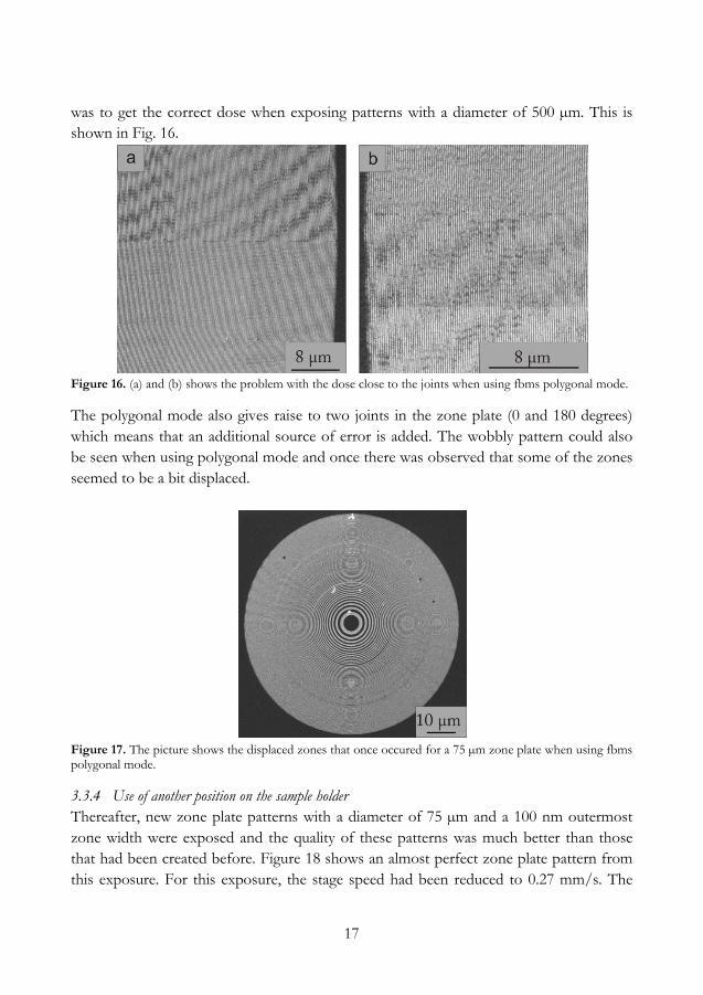
was to get the correct dose when exposing patterns with a diameter of 500 µm. This is shown in Fig. 16.
Figure 16. (a) and (b) shows the problem with the dose close to the joints when using fbms polygonal mode.
The polygonal mode also gives raise to two joints in the zone plate (0 and 180 degrees) which means that an additional source of error is added. The wobbly pattern could also be seen when using polygonal mode and once there was observed that some of the zones seemed to be a bit displaced.
Figure 17. The picture shows the displaced zones that once occured for a 75 µm zone plate when using fbms polygonal mode.
3.3.4 Use of another position on the sample holder Thereafter, new zone plate patterns with a diameter of 75 µm and a 100 nm outermost zone width were exposed and the quality of these patterns was much better than those that had been created before. Figure 18 shows an almost perfect zone plate pattern from this exposure. For this exposure, the stage speed had been reduced to 0.27 mm/s. The

18
sample was now also positioned at another clamp in the sample holder. This indicated that the stage performance could vary for different locations. However, it’s hard to tell if the new position on the sample holder or the reduced stage speed or a combination of both caused the improvements. Earlier experiences from my colleagues however, have indicated that the position in the sample holder at which the sample is positioned is of importance for the quality of the exposure.
Figure 18. The first results from exposure of a 75 µm zone plate pattern when the 2nd clamp on the sample holder was used. Stage speed = 0.27 mm/s.
Once again, a 75 µm zone plate with essentially the same parameters was exposed using the same clamp as during the last exposure, and the stage speed was 0.27 mm/s even this time. This time however, the exposure quality wasn’t as good as last time, as can be seen in Fig. 19.
Figure 19. 75 µm zone plate when the 2nd clamp on the sample holder was used. The pattern quality was worse this time compared to the last exposure. Stage speed = 0.27 mm/s.

19
3.3.5 Exposure of 500 µm diameter zone plates Throughout this diploma work, zone plate patterns with a diameter of 500 µm have been routinely exposed and those patterns were generally of a better quality than the 75 µm diameter zone plate patterns. The wobbly patterns that could be observed for the 75 µm zone plates were almost none existing for the 500 µm zone plate patterns. The problems with the joint error were generally much less for the 500 µm zone plates as well, although they weren’t completely eliminated. Figure 20 shows a 500 µm diameter zone plate with excellent quality over the whole pattern. The extra rings visible are not in the pattern but only a moiré-pattern caused by the circular rings on the rectangular pixel grid during the image scan.
Figure 20. A zone plate pattern with 500 µm diameter exposed with the FBMS module. The whole pattern is of very uniform quality. Figure 21 shows close-ups of two parts of a 500 µm diameter zone plate which shows a small problem with the stitching that occurs at the start/endpoint of a zone. In this case the stage speed was 0.31 mm/s. As can be seen in Fig. 21a, the joint error could be observed although they weren’t that severe. In Fig. 21b it is shown that the zone plate pattern was looking good in 270 degrees as well. Throughout the entire diploma work, it could be observed that the 500 µm zone plate had a better quality than the 75 µm zone plate. This was true even if the same parameters and stage speeds were used.

20
Figure 21. Close-ups of the outermost parts of a 500 µm diameter zone plate at 180 and 270 degrees respectively. As can be seen in (a), the joint error could be observed although they weren’t that severe. (b) shows that the zone plate pattern was looking good in 270 degrees.
4. Conclusion and discussion
As described in Sect. 3, many experiments have been executed in order to find out how good the fbms module works. Since it has been hard to obtain reproducible results it’s difficult to make certain conclusions. Sometimes the pattern was looking great after one exposure, whereas the next exposure gave a totally different outcome. However, there are some trends that often occurred that will be discussed in this section, and suggestions to future work will also be given. Many experiments have resulted in a pattern that is more or less wobbly. Sometimes this effect was almost negligible, whereas it was very apparent for other exposures. It was also clear that the zone plate pattern was more wobbly in some directions than in other. In zero degrees for instance, the pattern showed no signs of being wobbly for any of the exposures. The biggest problem with the pattern being wobbly could be observed in the angles 90, 135, 270 and 315 degrees. In between these angles the pattern could sometimes be perfect or almost perfect. The further away from the zone center, the bigger the problem normally was, although it sometimes could be exceptions to that. There have also been examples of exposures which have given a very periodic wobbly pattern, whereas the wobbly pattern seemed very random for other exposures or angles. All this combined with the difference in magnitude of the wobbly pattern indicates that there is

21
something wrong with the stage and that it’s not moving in a smooth path. Since the quality of the exposures varied so much from time to time, it’s plausible to assume that the stage suffers from some mechanical instability. This idea is supported by the fact that a humming noise that comes from one of the server motors can be heard when the stage is moved with the joystick. This cannot be heard during exposure but this can depend on that the stage speed during exposure is much lower compared to when the stage is being moved by using the joystick. This should be investigated further in the future. The vibration of the e-beam lithography system induced by the stage movement should also be measured in the future to see if that could be one cause of the problems. The attempt to reduce the stage speed by increasing the bias didn’t seem to have any influence of the quality of the exposure. Basically, the increase in dose per unit length is cancelled by the narrower zone. Another conclusion that could be drawn from the experiments is that it’s better to use fbms circle mode than polygonal mode when writing your pattern. This comes from the fact that it was difficult to get the correct dose close to the joints when using polygonal path. The polygonal mode yields two joints (instead for one which is the case for circle mode) and this adds another source of possible error. Besides, the problem with wobbly pattern couldn’t be avoided by using polygonal mode and the circle mode gave results that normally were at least as good as for the polygonal mode. Another thing that was observed was that the use of clamp in the sample holder could be of importance. At the beginning, only the clamp in the middle was used but then the 2nd clamp from left was used which gave a somewhat better result. However when this was done, other changes where done as well which lead to a reduced stage speed which makes it difficult to say whether it was the reduced stage speed that lead to the improvement, or if it was the use of another clamp. Anyway, the different outcome from different exposures with the same settings indicates that the exposure quality is dependent on the “day-status” of the e-beam lithography system. Although it’s hard to say whether the use of another clamp would have any effect on the exposure quality, this should be tested in the future. This means that the remaining clamps should be tested as well and each of the clamps has to be tested several times in order to see if any conclusions can be drawn. Earlier results from my colleagues have namely indicated that the choice of clamp might be of importance for the exposure quality. An important result of the conducted experiments is that the exposure of zone plate patterns with a diameter of 500 µm generally gave a better result than those with a diameter of 75 µm. This means that even if the 75 µm zone plate was wobbly, the 500 µm zone plate could be nearly perfect. One explanation to this is could be that the angular velocity of the stage for the larger zone plate is lower, which should give a better result.

22
The conclusion that can be drawn with this information is that the fbms mode should only be used when fabricating large zone plates, i.e. if it’s possible to expose the zone plate without using the fbms mode, it should be done instead. One important fact is that the exposure time for a 500 µm zone plate is a slightly longer than two hours, although the exposure time will vary depending on the dose factor and the beam current. This means however that it’s possible to expose one 500 µm zone plate in one exposure session, which typically is four hours. This also implies that it is possible to expose somewhat larger zone plate pattern without getting unpractical long exposure time. E.g., a 1 mm diameter zone plate could be estimated to take approximately 4 times as long if one only considers the increase in area. .

23
5. Acknowledgement
I would like to thank Prof. Hans Hertz, head of the BIOX division for giving me the opportunity of doing my diploma work in the nanofabrication group. I’m also very grateful to my supervisor Dr. Anders Holmberg who has helped me a lot during my diploma work. Besides I would like to give special thanks to Fredrik Uhlén and Julia Reinspach who’ve helped me a lot with the equipment in the nanofabrication lab and they’ve also given me valuable feedback during my work. I would also like to thank my family and friends for always supporting me. Last but not least I would like to thank everyone at the BIOX division for being so friendly.

24
6. Bibliography
[1] M.C. Teich, B.E.A. Saleh, Fundamentals of photonics.: John Wiley & Sons, 2007. [2] D. Attwood, Soft X-rays and extreme ultraviolet radiation.: Cambridge University Press,
1999. [3] J. Kirz, "Phase zone plates for x rays and the extreme uv," J. Opt. Soc. Am., 64, March
1974. [4] A. G. Michette, Optical systems for soft x rays. New York: Plenum Press, 1986. [5] F. Uhlén, "Nanofabrication process for tungsten zone plates," KTH - Applied
Physics, Stockholm, Diploma work 2010. [6] A. Holmberg, "Nanofabrication of Zone Plate Optics for Compact Soft X-Ray
Microscopy," KTH, Stockholm, Doctoral Thesis in Physics 2006. [7] S. Rehbein, A. Holmberg, G. Johansson, P. Jansson and H. Hertz, "Fabrication and
characterization of a condenser zone plate for compact x-ray microscopy," J. Vac. Sci Technol. B 22 1118, 2008.
[8] M.J. Rooks M.A. McCord, Microlithography, Micromaching, and Microfabrication, P. Rai-Choudhury, Ed.: SPIE, 1997, vol. 1: Microlithography.