lcd color television p 6 27wl5 technical training …diagramas.diagramasde.com/televisores/toshiba...
TRANSCRIPT
FILE NO. 036-200501
TECHNICAL TRAINING MANUAL
LCD COLOR TELEVISION
PRINTED IN JAPAN, Nov., 2005 S
27WL56P32WL56P37WL56P
���������������� 1-1, SHIBAURA 1-CHOME, MINATO-KU, TOKYO 105-01, JAPAN

Capture 1 Outline
1-1 Construction:・ This is a portable type colour television receiver with a 32 inches wide
・ Full Square picture tube (800.0 mm measured on diagonal of viewable picture area)
・ 1. Cabinet:
・ The cabinet is constructed with 2 parts. They are molded front cabinet and back cover.
・ The molded front cabinet is made of polystyrene, the back cover and bezel are also made
・ of polystyrene.( In addition, there is a stand.)
・ 2. Chassis:
・ This model is constructed of a 3 units. One is the POWER/AC-IN unit,
・ one is SIGNAL unit, and the other one is the AV-OTHER unit.
・ There are 8 printed circuit boards
・ (IF-AV, SIGNAL, POWER, AC-IN, LED/RMT, KEY-SW, PC-IN, and FRONT-AV board).
・ 3. LCD Panel:
・ This model is equipped with the LCD panel of W-XGA(1366 x768 pixel) of an aspect ratio 16:9.
1-1

4. Circuitry:・ a) This model is provided with Frequency Synthesis Tuning system,・ so those channels can be stored in 100 pre-set program position, which can be・ easily selected.・ b) This model can receive,・ from Antenna: PAL-BG/DK/I, SECAM-BG/DK/L and 4.43NTSC-BG system.・ from AV Input: PAL(50&60Hz), SECAM(50Hz), NTSC(50Hz) and
3.58/4.43NTSC・ c) This model has 2 SCART pin (21pin) connectors so that you can connect various・ external units.・ d) This model is equipped with S-Video Input Terminal (Front), PC/RGB Input Terminal
(Rear)・ and HDMI Input Terminal for DVD (Rear).・ e) This model is provided with head-phone socket and AV Input Terminals (Front).・ f) This model is equipped with 6 screen modes.・ (SUPER LIVE/CINEMA/SUBTITLE/14:9/WIDE/4:3 mode)・ g) This model is equipped with Sound Multiplex Processing Circuit.・ (NICAM-L/I/BG, IGR-BG/DK system)・ h) This model is equipped with ON-TIMER and SLEEP-TIMER.・ i) This model is equipped with TELETEXT(2,100pages) Receiving system. And Level 2.5
system・ j) This model is equipped with “WOW SRS 3D” system.・ k) This model is equipped with ATS system.
1-2

32・37WL56P
REARAV
POWER
AC IN
SIGNAL
LED
KEY
FRONTAV
SCART
SCART
2P
3P
RCA×3、S×1
TU RGB/PC HDMI
FFCCable
LVDSCable
SP SP
HP
1-2 PCB Layout Representative 32-37 size
1-3
PCB Layout Representative 32 size
23
26 32
Signal
AV
POWER
AC-INPUT
1-4
1-3 Commonness of PCB
Domestic Japan
USA
AJIA
Euro
US
JPN
Main Power
AC,Low-BSignal
23~26 32
WIDE POWER
Supply
Other..etc
(AV,Key,LED,CARD..etc)
Common(Only Soft)
20
① ② ③ ④
⑤
⑥
⑦
⑧
⑨
23LC100
37HL95
27/32/37WL55C
27/32/37WL56P
Digital
Common
Individual change(Jack shape etc.)
Digital Unit27/32/37WL55EAT
China
1-5
- + ▼ ▲MENU P
∧∨><OK
TOSHIBA
1-4 LCD TV Operation arrangement and display specification
( 3 )
AUDIO
VIDEO
R
L/MONO( 3 )
AUDIO
VIDEO
R
L/MONO
Model Name 27WL56P +-MENU P
OK
1-6
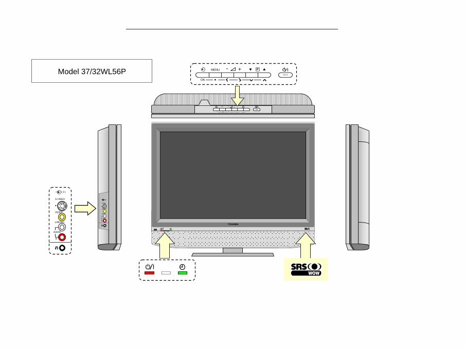
- + ▼ ▲MENU P
∧∨><OK
TOSHIBA
+-MENU P
OK
VIDEO
AUDIO
R
L/MONO
S-VIDEO
( 3 )
▶VIDEO
AUDIO
R
L/MONO
S-VIDEO
( 5 )( 5 )
▶
Model 37/32WL56P
LCD TV Operation arrangement and display specification
1-7
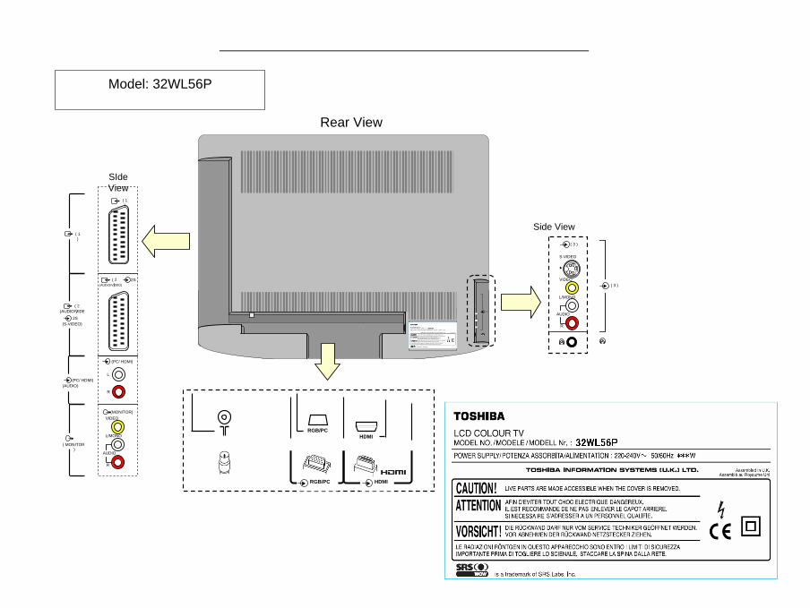
SIdeView
( 1 )
( 1 )
( 2 )(AUDIO/VIDEO)
2S
( 2 )
2S(AUDIO/VIDEO)
(S-VIDEO)
( MONITOR)
VIDEO
AUDIO
R
L/MONO
(MONITOR)
(AUDIO)R
L
(PC/ HDMI)
(PC/ HDMI)
Rear View
( 5 )
Side View
( 3 )VIDEO
AUDIO
R
L/MONO
S-VIDEO
( 3 )
▶
Model: 32WL56P
RGB/PC
RGB/PC
HDMI
HDMI
LCD TV Operation arrangement and display specification
1-8
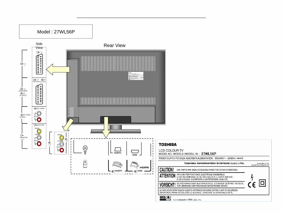
Rear View
Model : 27WL56P
Side View
( 1 )
( 1 )
( 2 )(AUDIO/VIDEO)
2S
( 2 )
2S(AUDIO/VIDEO)
(S-VIDEO)
( MONITOR)
VIDEO
AUDIO
R
L/MONO
(MONITOR)
(AUDIO)
(PC/ HDMI)
(PC/ HDMI)
R
L
AUDIO
RGB/PC
RGB/PC
HDMI
HDMI
(S-VIDEO)
( 3 )
( 3 )
VIDEO
AUDIO
R
L/MONO
LCD TV Operation arrangement and display specification
1-9
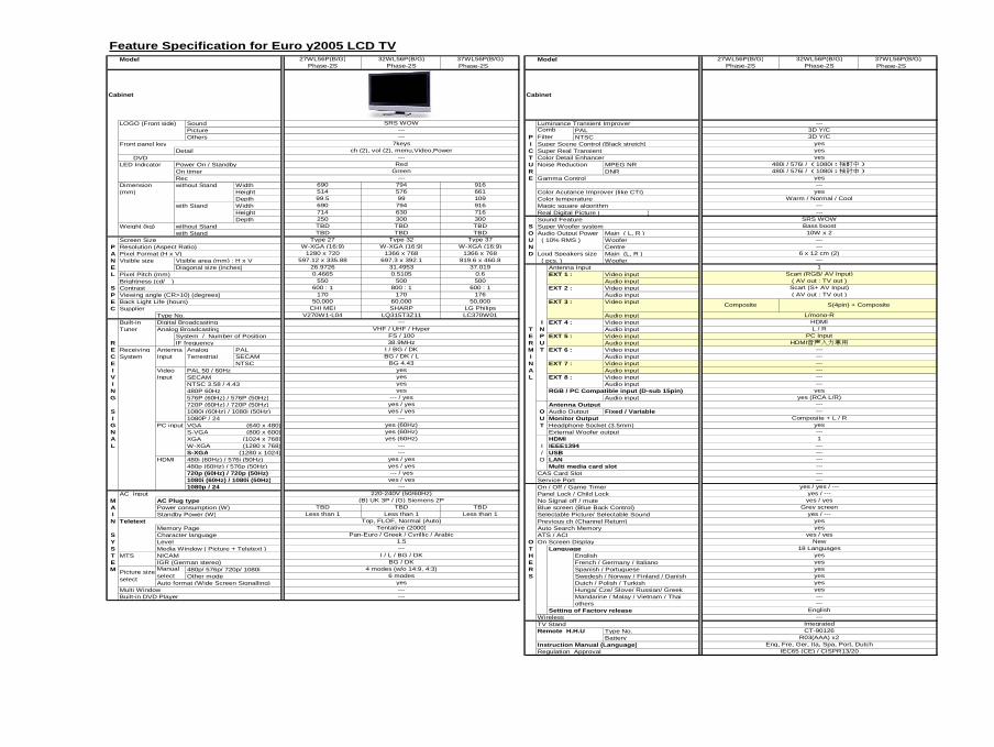
Feature Specification for Euro y2005 LCD TVModel Model
Cabinet Cabinet
LOGO (Front side) Sound Luminance Transient ImproverPicture PALOthers P NTSC
Front panel key I Super Scene Control (Black stretch)Detail C Super Real Transient
内蔵DVD操作キー T Color Detail EnhancerLED Indicator Power On / Standby U Noise Reduction MPEG NR
On timer R DNRRec E Gamma Control
Dimension without Stand Width Color Management(mm) Height Color Acutance Improver (like CTI)
Depth Color temperaturewith Stand Width Magic square algorithm
Height Real Digital Picture (デジタル一貫処理)Depth Sound Feature
Weight (kg) without Stand S Super Woofer systemwith Stand O Audio Output Power Main ( L, R )
Screen Size U ( 10% RMS ) WooferP Resolution (Aspect Ratio) N CentreA Pixel Format (H x V) D Loud Speakers size Main (L, R )N Visible size Visible area (mm) : H x V ( pcs. ) WooferE Diagonal size (inches) Antenna InputL Pixel Pitch (mm) EXT 1 : Video input
Brightness (cd/㎡) Audio inputS Contrast EXT 2 : Video inputP Viewing angle (CR>10) (degrees) Audio inputE Back Light Life (hours) EXT 3 : Video inputC Supplier
Type No. Audio inputBuilt-in Digital Broadcasting I EXT 4 : Video inputTuner Analog Broadcasting T N Audio input
System / Number of Position E P EXT 5 : Video inputR IF frequency R U Audio inputE Receiving Antenna Analog PAL M T EXT 6 : Video inputC System Input Terrestrial SECAM I Audio inputE NTSC N EXT 7 : Video inputI Video PAL 50 / 60Hz A Audio inputV Input SECAM L EXT 8 : Video inputI NTSC 3.58 / 4.43 Audio inputN 480P 60Hz RGB / PC Compatible input (D-sub 15pin)G 576P (60Hz) / 576P (50Hz) Audio input
720P (60Hz) / 720P (50Hz) Antenna OutputS 1080i (60Hz) / 1080i (50Hz) O Audio Output Fixed / VariableI 1080P / 24 U Monitor OutputG PC input VGA (640 x 480) T Headphone Socket (3.5mm) N S-VGA (800 x 600) External Woofer outputA XGA (1024 x 768) HDMIL W-XGA (1280 x 768) I IEEE1394
S-XGA (1280 x 1024) / USBHDMI 480i (60Hz) / 576i (50Hz) O LAN
480p (60Hz) / 576p (50Hz) Multi media card slot720p (60Hz) / 720p (50Hz) CAS Card Slot1080i (60Hz) / 1080i (50Hz) Service Port1080p / 24 On / Off / Game Timer
AC Input Panel Lock / Child LockM AC Plug type No Signal off / muteA Power consumption (W) Blue screen (Blue Back Control)I Standby Power (W) Selectable Picture/ Selectable SoundN Teletext Previous ch (Channel Return)
Memory Page Auto Search MemoryS Character language ATS / ACIY Level O On Screen DisplayS Media Window ( Picture + Teletext ) T LanguageT MTS NICAM H EnglishE IGR (German stereo) E French / Germany / ItalianoM 480p/ 576p/ 720p/ 1080i R Spanish / Portuguese
Other mode S Swedesh / Norway / Finland / DanishAuto format (Wide Screen Signalling) Dutch / Polish / Turkish
Multi Window Hunga/ Cze/ Slove/ Russian/ GreekBuilt-in DVD Player Mandarine / Malay / Vietnam / Thai
othersSetting of Factory release
WirelessTV StandRemote H.H.U Type No.
BatteryInstruction Manual (Language)Regulation Approval
Eng, Fre, Ger, Ita, Spa, Port, DutchIEC65 (CE) / CISPR13/20
CT-90126R03(AAA) x2
---Integrated
---English
yes---
yesyes
yesyes
18 Languagesyes
yes / yesNew
yesyes
Grey screenyes / ---
yes / ---yes / yes
------
yes / yes / ---
---------
1---
yes---
---Composite + L / R
yes (RCA L/R)---
------yes
------
------
PC InputHDMI音声入力兼用
L/mono-RHDMIL / R
( AV out : TV out )
Composite S(4pin) + Composite
( AV out : TV out )Scart (S+ AV Input)
1Scart (RGB/ AV Input)
6 x 12 cm (2)---
------
Bass boost10W x 2
---SRS WOW
Warm / Normal / Cool---
---yes
480i / 576i / (1080i:検討中)
yes
yes480i / 576i / (1080i:検討中)
yesyes
3D Y/C3D Y/C
---
27WL56P(B/G) 32WL56P(B/G) 37WL56P(B/G)Phase-2S Phase-2S Phase-2S展開
CombFilter
---
yes---
4 modes (w/o 14:9, 4:3)6 modesPicture size
select
Manualselect
BG / DKI / L / BG / DK
---1.5
Pan-Euro / Greek / Cyrillic / ArabicTentative (2000)
Top, FLOF, Normal (Auto)
TBD TBD TBDLess than 1 Less than 1 Less than 1
(B) UK 3P / (G) Siemens 2P
---220-240V (50/60Hz)
--- / yesyes / yes
yes / yesyes / yes
------
yes (60Hz)yes (60Hz)yes (60Hz)
---yes / yesyes / yes--- / yes
yesyesyesyes
BG 4.43BG / DK / LI / BG / DK38.9MHzFS / 100
VHF / UHF / Hyper
V270W1-L04 LQ315T3Z11 LC370W01---
60,000 50,000CHI MEI SHARP LG Philips50,000
800 : 1 600 : 1170 170 176
600 : 1
0.4665 0.5105 0.6550 500 500
597.12 x 335.88 697.3 x 392.1 819.6 x 460.826.9726 31.4953 37.019
W-XGA (16:9) W-XGA (16:9)1280 x 720 1366 x 768 1366 x 768
W-XGA (16:9)
TBD TBD TBDType 27 Type 32 Type 37
250 300 300TBD TBD TBD
690 794 916714 630 716
514 576 66199.5 99 109
---690 794 916
Green
---Red
ch (2), vol (2), menu,Video,Power7keys
------
SRS WOW
27WL56P(B/G) 32WL56P(B/G) 37WL56P(B/G)Phase-2S Phase-2S Phase-2S展開
1-5
1-10

2-1
Chapter 2. Analog Signal Reception circuit
2.1 Outline
Receiving Frequency Range 48.25~855.25MHz
Receiving RF System BG,I,DK,L
High Performance Split carrier IF receiving module unit
TIF module (H001) is consisting of the Tuner and IF blocks.
SIF signal corresponding to the receiving RF system is demodulated in MSP (Multi Sound Processor)
in IC600.
RF system switching is performed by controlling the switching circuit in IC TDA9886 on TIF module
through IIC Bus line.
When receiving L-system VHF Low Band signal, IF frequency is switched accordingly.
Fig 2-1 Analog Signal Reception Circuit Block
AV UNIT
H001 TUNER
SIGNAL UNIT
IC600 MSP
IC700 Cortez
SIF
V-TV
ANT
2-2
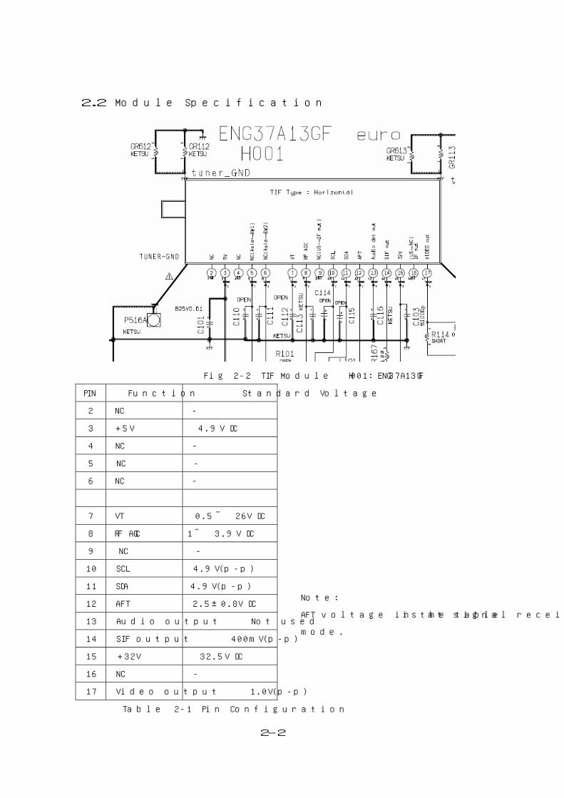
2.2 Module Specification
Fig 2-2 TIF Module H001:ENG37A13GF
PIN Function Standard Voltage
2 NC -
3 +5V 4.9V DC
4 NC -
5 NC -
6 NC -
7 VT 0.5 ̃ 26V DC
8 RF AGC 1 ̃ 3.9V DC
9 NC -
10 SCL 4.9V(p-p)
11 SDA 4.9V(p-p)
12 AFT 2.5±0.8V DC
13 Audio output Not used
14 SIF output 400mV(p-p)
15 +32V 32.5V DC
16 NC -
17 Video output 1.0V(p-p)
Table 2-1 Pin Configuration
Note:
AFT voltage in the table is at signal receiving
mode.

2-3
2.3 Troubleshooting
1)No Picture output
YES
Yes
Yes
YES
No
YES
NO
NO
No Picture
H001 Check voltage at #3:5V、#15:32V
Check the power supply circuit
Check that the voltage at #7 of H001 varies when changing CH position.
Check the waveform at #17 (approx. 1Vp-p)
H001 is OK. Check the
circuits after H001.
BUS line patter open or Check Connector fitting
Check the voltage at #10 and 11. Check the waveform at BUS line (approx. 4.9Vp-p)
Replace H001
Check that the voltage at #8 varies more than 3.5V at no signal receiving. Replace H001
Replace H001
No
NO
2-4
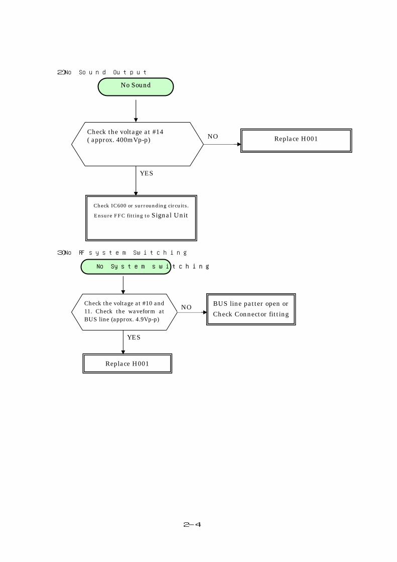
2)No Sound Output
3)No RF system Switching
YES
No Sound
Replace H001 Check the voltage at #14 ( approx. 400mVp-p)
Check IC600 or surrounding circuits.
Ensure FFC fitting to Signal Unit
NO
YES
No System switching
BUS line patter open or Check Connector fitting
Check the voltage at #10 and 11. Check the waveform at BUS line (approx. 4.9Vp-p)
Replace H001
NO
3-1
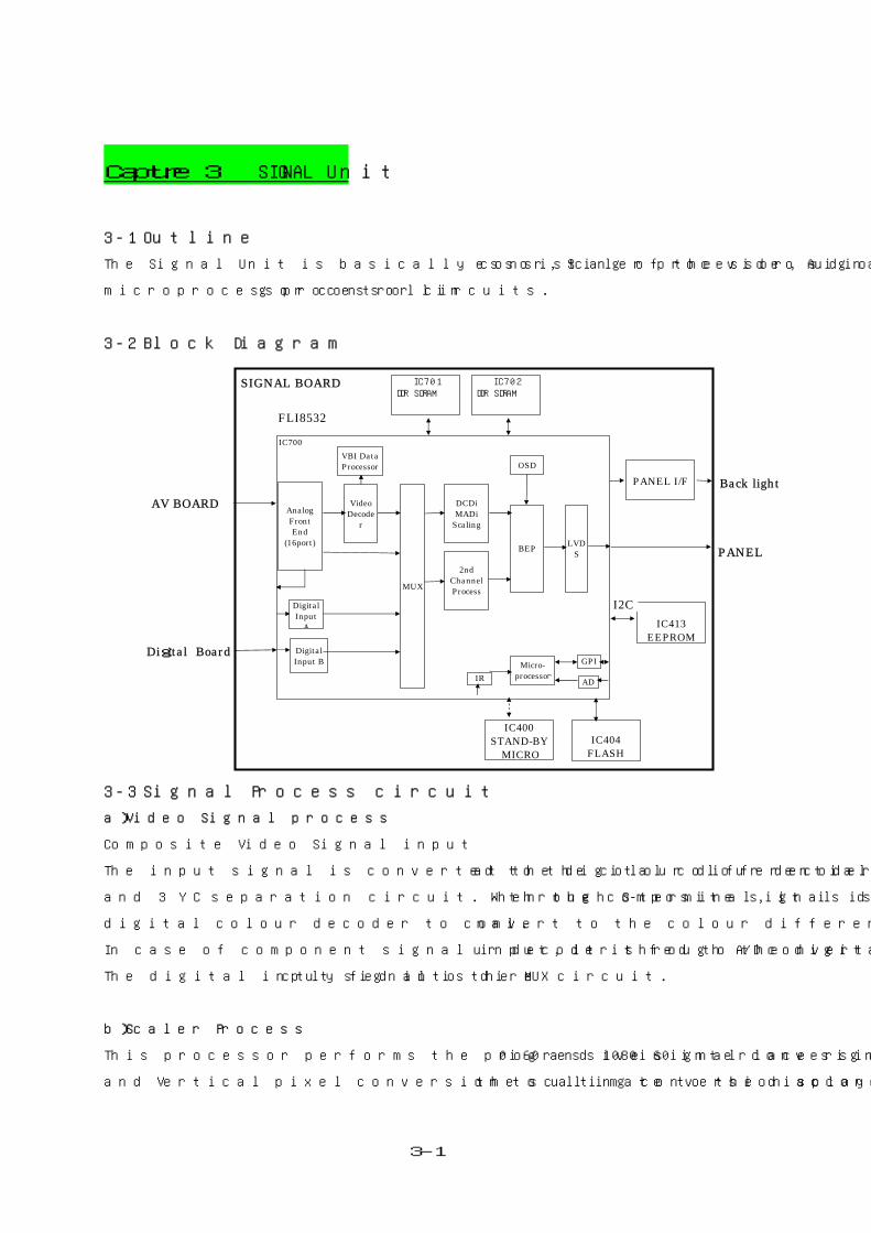
Capture 3 SIGNAL Unit
3-1 Outline
The Signal Unit is basically consisting of the video signal processor, Scaler processor, Audio signal processor and
microprocessor controlling processor circuits.
3-2 Block Diagram
IC700
AnalogFrontEnd
(16port)
VideoDecode
r
MUX
VBI DataProcessor
DCDiMADi
Scaling
BEP
OSD
LVDS
Micro-processorIR AD
GPI
DigitalInput
A
DigitalInput B
2ndChannelProcess
IC400STAND-BY
MICRO
IC701DDR SDRAM
IC413EEPROM
IC702DDR SDRAM
IC404FLASH
I2C
SIGNAL BOARD
FLI8532
AV BOARD
Digital Board
Back lightPANEL I/F
PANEL
3-3 Signal Process circuit
a)Video Signal process
Composite Video Signal input
The input signal is converted to the colour differential signal at the digital colour decoder through A/D converter
and 3 YC separation circuit. When the composite signal is input through S-terminal, it is directly fed into the
digital colour decoder to convert to the colour differential signal.
In case of component signal input, it is fed to the digital colour decoder through A/D converter.
The digital input signal is directly fed into the MUX circuit.
b)Scaler Process
This processor performs the progressive signal conversion for 480i60 and 1080i60 interlace signal, the Horizontal
and Vertical pixel conversion to ultimate to the display panel, the scaling conversion according to the picture size
3-2
and the insertion of OSD signal from SEINE.
IC701 and IC702 (DDR-SDRAM) are for the progressive conversion and the scaling process.
c) Back End Processor
This functions various picture controls such as Contrast, Colour, TINT, Sharpness and Black level and also for
Dynamic gamma collection, colour management, colour matrix and RGB gamma collection.
d) LVDS
The interface signal LVDS generated in IC400 and IC700 is fed to the panel.
3-4 Microprocessor control process
There are two microprocessors of IC400 (Stand-by microprocessor) and IC 700 (FLI8532).
The Firmware in Stand-by microprocessor IC400 is possible to rewriting.
The program for IC700 is stored in IC404 Flash Memory and it is possible to rewriting.
IC 700 controls IC400 through IIC BUS line.
To control power On or Off is shown below. I/O expansion on IC700 is used for LED control, S1/S2 detection and
so on by using I/O expander.
The microprocessor in IC700 is controlled by Seine microprocessor via UART and also it controls IC700 itself,
multiplex sound IC, analogue tuner and others.
Power On Control
Power Off Control
The default data for IC700 is stored in E2PROM.
Power On
command received
in IC400
Turn IC700
power on. User action
Power Off
command
received in IC700
IC 700 feeds a
power off
command to
IC400
IC400 turns
IC700 off. User action
3-3
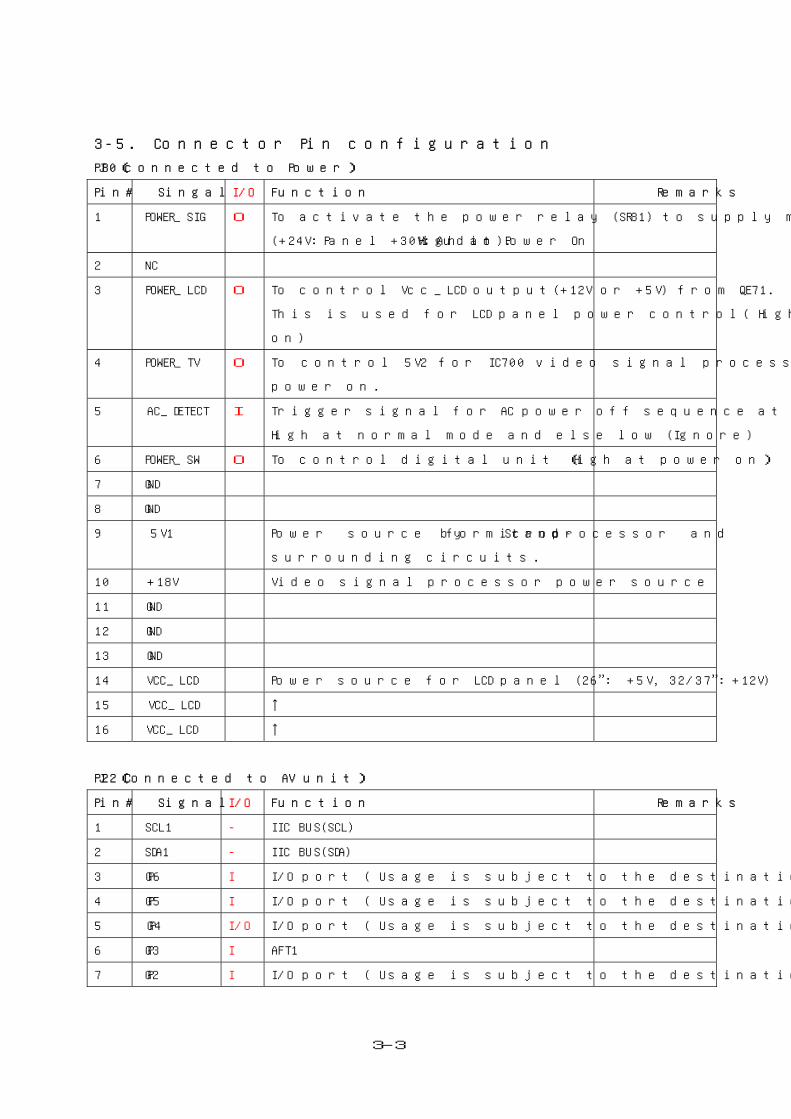
3-5. Connector Pin configuration
PJ80(connected to Power)
Pin# Singal I/O Function Remarks
1 POWER_SIG O To activate the power relay (SR81) to supply main power
(+24V:Panel +30V:Audio). High at Power On
2 NC
3 POWER_LCD O To control Vcc_LCD output(+12V or +5V) from QE71.
This is used for LCD panel power control( High at power
on)
4 POWER_TV O To control 5V2 for IC700 video signal process. High at
power on.
5 AC_DETECT I Trigger signal for AC power off sequence at AC power off.
High at normal mode and else low (Ignore)
6 POWER_SW O To control digital unit (High at power on)
7 GND
8 GND
9 5V1 Power source for Stand-by microprocessor and
surrounding circuits.
10 +18V Video signal processor power source
11 GND
12 GND
13 GND
14 VCC_LCD Power source for LCD panel (26”: +5V, 32/37”:+12V)
15 VCC_LCD ↑
16 VCC_LCD ↑
PJ22(Connected to AV unit)
Pin# Signal I/O Function Remarks
1 SCL1 - IIC BUS(SCL)
2 SDA1 - IIC BUS(SDA)
3 GP6 I I/O port ( Usage is subject to the destination)
4 GP5 I I/O port ( Usage is subject to the destination)
5 GP4 I/O I/O port ( Usage is subject to the destination)
6 GP3 I AFT1
7 GP2 I I/O port ( Usage is subject to the destination)
3-4
8 GP1 O I/O port ( Usage is subject to the destination)
9 MOUT O IC700 MONITOR Signal output 1Vp-p
10 GND MONITOR Signal GND
11 C_BS Not in use
12 Y_BS Not in use
13 V_BS_GND GND
14 V_BS O Not in use (In use for digital unit incorporated ) 2Vp-p
15 RET I ADC SV RETURN Terminal
16 GND GND
17 C4 I ADC C Ch4 video input
18 GND GND
19 B4 I ADC B Ch4video input
20 GND GND
21 A4 ADC A Ch4 video input
22 GND GND
23 SV4 I ADC SV Ch4 video input
24 RET ADC C RETURN
25 GND GND
26 C3 I ADC C Ch3 video input (TV) 1Vp-p
27 GND GND
28 B3 ADC B Ch3 video input
29 GND GND
30 A3 I ADC A Ch3 video input
31 GND GND
32 SV3 ADC SV Ch3 video input
33 RET ADC B RETURN
34 GND GND
35 C2 I ADC C Ch2 video input
36 GND GND
37 B2 I ADC B Ch2 video input
38 GND GND
39 A2 I ADC A Ch2 video input
40 GND GND
41 SV2 ADC SV Ch2 video input
42 RET ADC A RETURN

3-5
43 GND GND
44 B1 I ADC B Ch1 video input
45 GND GND
46 C1 I ADC C Ch1 video input
47 GND GND
48 SV1 ADC SV Ch1 video input
49 GND GND
50 A1 I ADC A Ch1 video input
PJ21(Connected to AV unit)
Pin# Signal I/O Function remarks
1 5V2 Power source for IC700 Analogue signal process
2 GND
3 9V Power source for Analogue signal process
PJ42(Connected to KEY)
Pin# Signal I/O Function remarks
1 KEY3 I Local key for HDD ( only with HDD incorporated)
2 POWER_KE
Y
I Power On/Off Key
3 KEY2 I Receiving signal/input signal selection key
4 GND
5 KEY1 I Channel +/-、Volume +/- Key
6 KEY GND
PJ41(Connected to IR)
Pin# Signal I/O Function remarks
1 BS_ROKUG
A
O Status LED control
2 SHIYOUTHU O Network using LED control
3 LED(TAIKI) O Stand-by LED control
4 GND
5 ROKUGA_Y
OYAKU
O Timer Recording LED control
6 JYUZOU_LE O Power On LED control

3-6
D
7 5V1 Power source for Stand-by microprocessor and
surrounding circuits
8 GND
9 RMT_IN I Remote signal reception signal
10 3.3V Remote sensor power source
11 RMT_FGND
PJ404(Flash Firmware rewriting)
Pin# Signal I/O Function remarks
1 5V2
2 ATXD O IC404(Flash Memory) rewriting
3 - Not in use
4 - Not in use
5 GND
6 SDA0 I IC413(E2P ROM)rewriting
7 - Not in use
8 - Not in use
9 SUB_CL
K
I IC400(Standby microprocessor )rewriting
10 SUB_PG
M
I IC400(Standby microprocessor)rewriting
11 GND
12 - Not in use
13 GND
14 - Not in use
15 - Not in use
16 - Not in use
17 - Not in use
18 - Not in use
19 - Not in use
20 - Not in use
21 ARXD I IC404(Flash Memory)rewriting
22 GND
23 /RESET I IC700 Reset
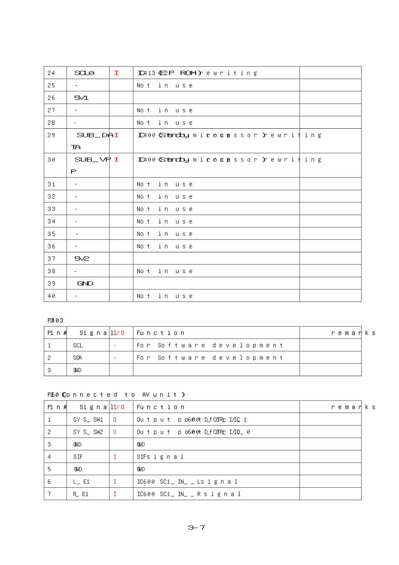
3-7
24 SCL0 I IC413(E2P ROM)rewriting
25 - Not in use
26 5V1
27 - Not in use
28 - Not in use
29 SUB_DA
TA
I IC400(Standby microprocessor)rewriting
30 SUB_VP
P
I IC400(Standby microprocessor)rewriting
31 - Not in use
32 - Not in use
33 - Not in use
34 - Not in use
35 - Not in use
36 - Not in use
37 5V2
38 - Not in use
39 GND
40 - Not in use
PJ403
Pin# Signal I/O Function remarks
1 SCL - For Software development
2 SDA - For Software development
3 GND
PJ60(Connected to AV unit)
Pin# Signal I/O Function remarks
1 SYS_SW1 O Output port for IC600 D_CTR_I/_1
2 SYS_SW2 O Output port for IC600 D_CTR_I/O_0
3 GND GND
4 SIF I SIFsignal
5 GND GND
6 L_E1 I IC600 SC1_IN__Lsignal
7 R_E1 I IC600 SC1_IN__R signal
3-8
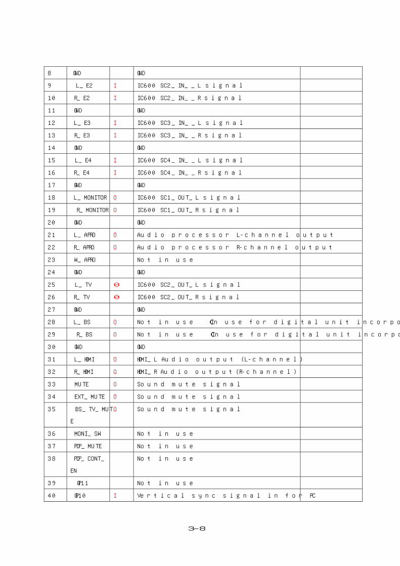
8 GND GND
9 L_E2 I IC600 SC2_IN__L signal
10 R_E2 I IC600 SC2_IN__R signal
11 GND GND
12 L_E3 I IC600 SC3_IN__L signal
13 R_E3 I IC600 SC3_IN__R signal
14 GND GND
15 L_E4 I IC600 SC4_IN__L signal
16 R_E4 I IC600 SC4_IN__R signal
17 GND GND
18 L_MONITOR O IC600 SC1_OUT_L signal
19 R_MONITOR O IC600 SC1_OUT_R signal
20 GND GND
21 L_APRO O Audio processor L-channel output
22 R_APRO O Audio processor R-channel output
23 W_APRO Not in use
24 GND GND
25 L_TV 0 IC600 SC2_OUT_L signal
26 R_TV 0 IC600 SC2_OUT_R signal
27 GND GND
28 L_BS O Not in use (In use for digital unit incorporated )
29 R_BS O Not in use (In use for digital unit incorporated )
30 GND GND
31 L_HDMI O HDMI_L Audio output (L-channel)
32 R_HDMI O HDMI_R Audio output(R-channel)
33 MUTE O Sound mute signal
34 EXT_MUTE O Sound mute signal
35 BS_TV_MUT
E
O Sound mute signal
36 MONI_SW Not in use
37 PDP_MUTE Not in use
38 PDP_CONT_
EN
Not in use
39 GP11 Not in use
40 GP10 I Vertical sync signal in for PC

3-9
41 GP9 I Horizontal sync signal in for PC
42 ATXD Not in use
43 SW_DVI1 O IC700 AE23 output port
44 SW_DVI2 O IC700 AF22 output port
45 STOP_FAN I FAN STOP detection ( not in use )
46 POWER_LN
B
O Power On/Off signal for LNB power unit
47 LR_LNB O To select power voltage of LNB power unit
48 SHORT_LNB I To detect short circuit on LNB power unit
49 GP8 I SW2 signal for TELTEXT ( TXT model only )
50 GP7 I SW1 signal for TELTEXT ( TXT model only )
PJ910(Connected to display panel)
Pin# Signal I/O Function remarks
1 Vcc +5V or +12V power line
2 Vcc +5V or +12V power line
3 Vcc +5V or +12V power line
+5V:26” only
+12V:others
4 Vcc +5V or +12V power line
5 GND GND
6 GND GND
7 GND GND
8 GND GND
9 Select
LVDS Data
format
O To select data mapping
0V
10 NC NC
11 GND GND
12 RA- O LVDS CH A data signal - VOC=1.25V
13 RA+ O LVDS CH A data signal + VOD=500mV
14 GND GND
15 RB- O LVDS CH B data signal - VOC=1.25V
16 RB+ O LVDS CH B data signal + VOD=500mV
17 GND GND
18 RC- O LVDS CH C data signal - VOC=1.25V
19 RC+ O LVDS CH C data signal + VOD=500mV
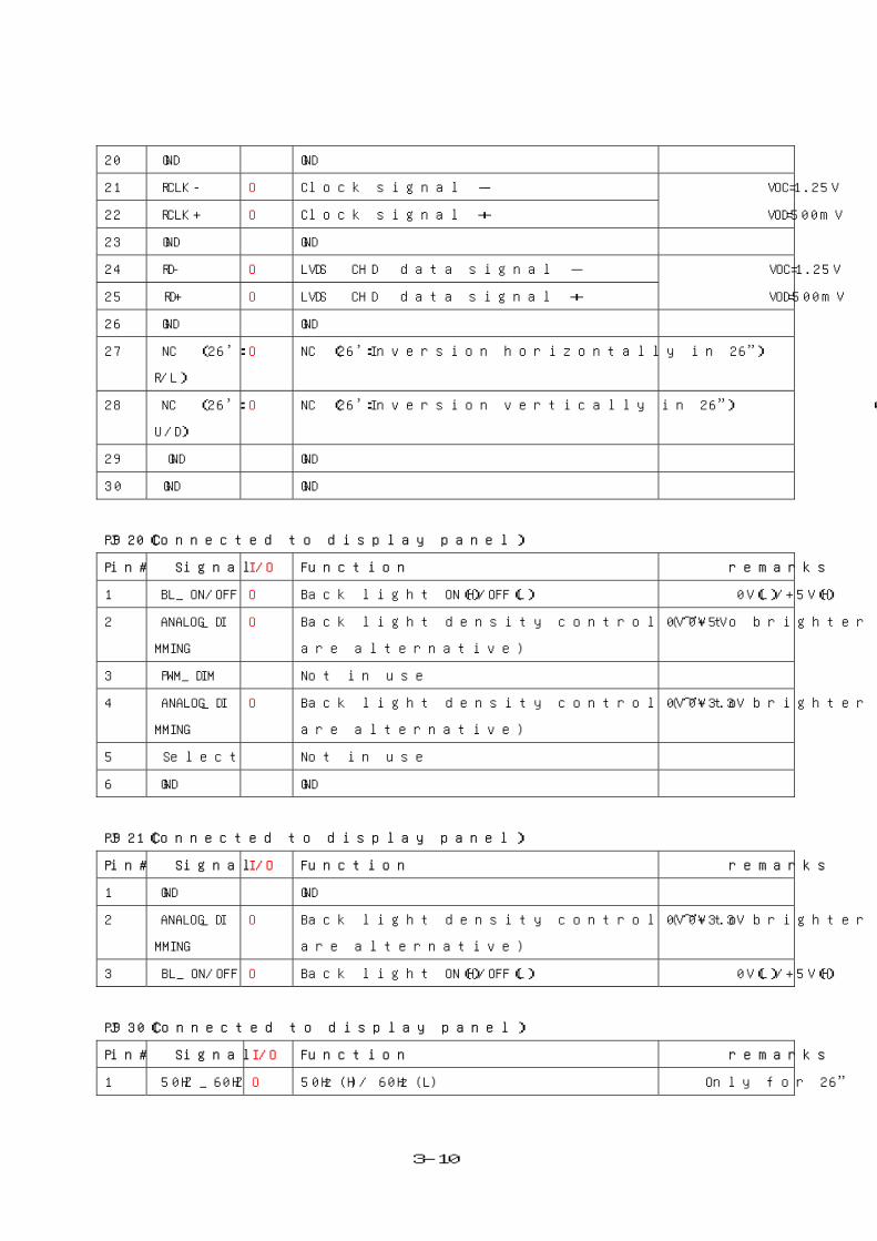
3-10
20 GND GND
21 RCLK- O Clock signal - VOC=1.25V
22 RCLK+ O Clock signal + VOD=500mV
23 GND GND
24 RD- O LVDS CH D data signal - VOC=1.25V
25 RD+ O LVDS CH D data signal + VOD=500mV
26 GND GND
27 NC ( 26’ :
R/L)
O NC (26’:Inversion horizontally in 26”) 0V:26’
28 NC ( 26’ :
U/D)
O NC (26’:Inversion vertically in 26”) 0V:26’
29 GND GND
30 GND GND
PJ920(Connected to display panel)
Pin# Signal I/O Function remarks
1 BL_ON/OFF O Back light ON(H)/OFF(L) 0V(L)/+5V(H)
2 ANALOG_DI
MMING
O Back light density control ( 0V to brighter on 26”, others
are alternative)
0V~+5V
3 PWM_DIM Not in use
4 ANALOG_DI
MMING
O Back light density control ( 0V to brighter on 26”, others
are alternative)
0V~+3.3V
5 Select Not in use
6 GND GND
PJ921(Connected to display panel)
Pin# Signal I/O Function remarks
1 GND GND
2 ANALOG_DI
MMING
O Back light density control ( 0V to brighter on 26”, others
are alternative)
0V~+3.3V
3 BL_ON/OFF O Back light ON(H)/OFF(L) 0V(L)/+5V(H)
PJ930(Connected to display panel)
Pin# Signal I/O Function remarks
1 50HZ_60HZ O 50Hz(H)/ 60Hz(L) Only for 26”
3-11
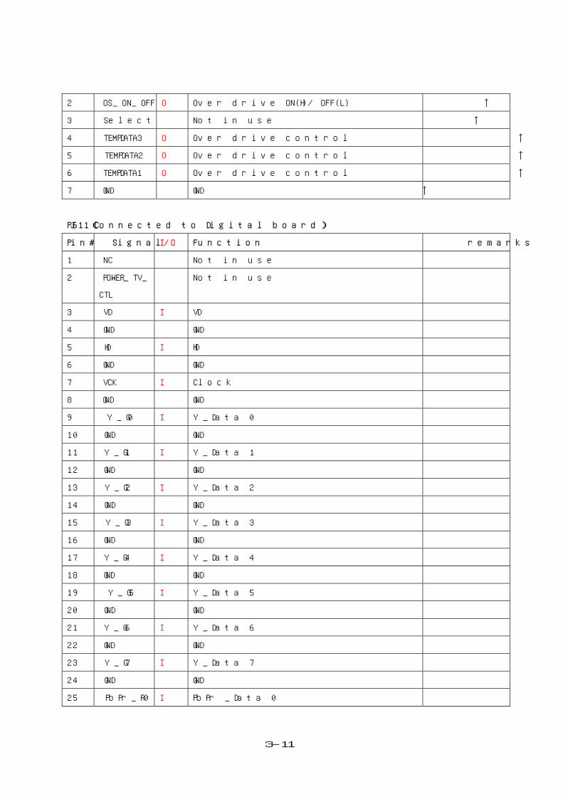
2 OS_ON_OFF O Over drive ON(H)/ OFF(L) ↑
3 Select Not in use ↑
4 TEMPDATA3 O Over drive control ↑
5 TEMPDATA2 O Over drive control ↑
6 TEMPDATA1 O Over drive control ↑
7 GND GND ↑
PJ611(Connected to Digital board)
Pin# Signal I/O Function remarks
1 NC Not in use
2 POWER_TV_
CTL
Not in use
3 VD I VD
4 GND GND
5 HD I HD
6 GND GND
7 VCK I Clock
8 GND GND
9 Y_G0 I Y_Data 0
10 GND GND
11 Y_G1 I Y_Data 1
12 GND GND
13 Y_G2 I Y_Data 2
14 GND GND
15 Y_G3 I Y_Data 3
16 GND GND
17 Y_G4 I Y_Data 4
18 GND GND
19 Y_G5 I Y_Data 5
20 GND GND
21 Y_G6 I Y_Data 6
22 GND GND
23 Y_G7 I Y_Data 7
24 GND GND
25 PbPr_R0 I PbPr _Data 0
3-12
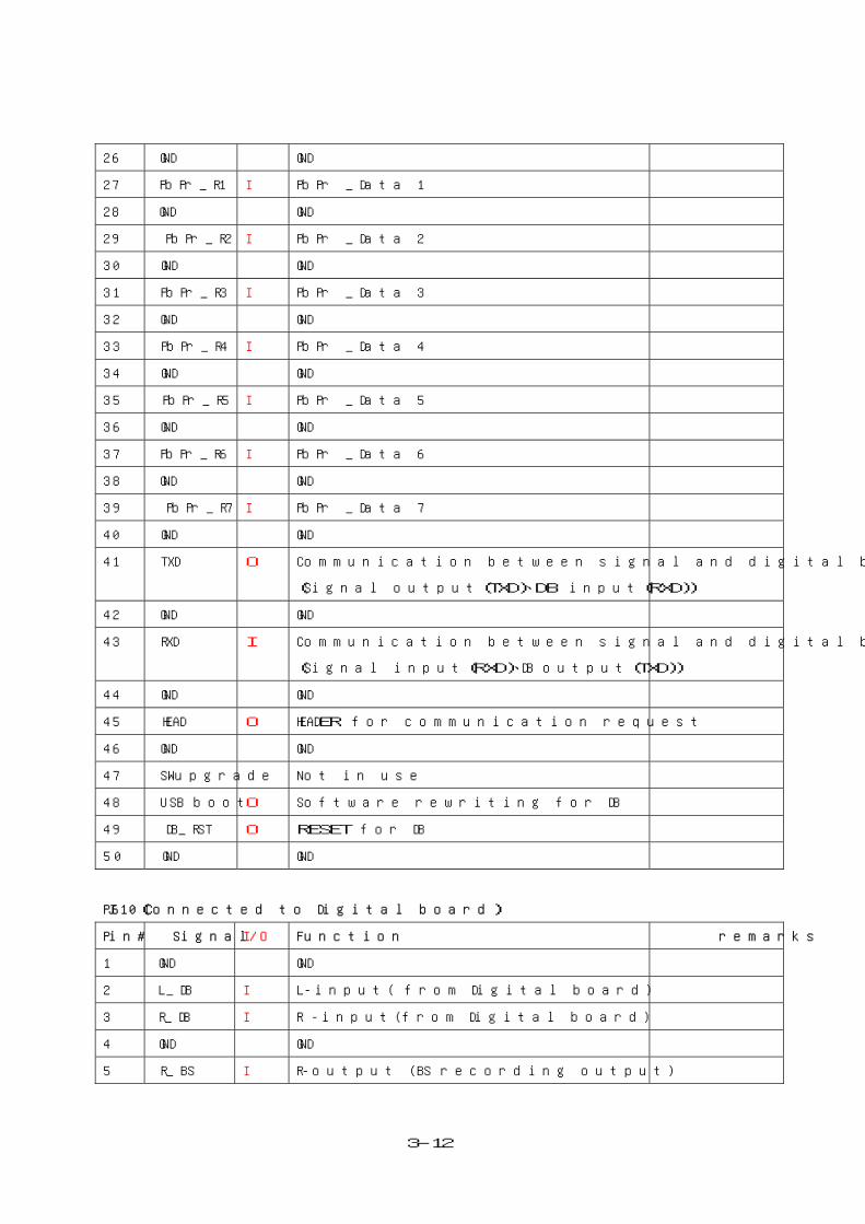
26 GND GND
27 PbPr_R1 I PbPr _Data 1
28 GND GND
29 PbPr_R2 I PbPr _Data 2
30 GND GND
31 PbPr_R3 I PbPr _Data 3
32 GND GND
33 PbPr_R4 I PbPr _Data 4
34 GND GND
35 PbPr_R5 I PbPr _Data 5
36 GND GND
37 PbPr_R6 I PbPr _Data 6
38 GND GND
39 PbPr_R7 I PbPr _Data 7
40 GND GND
41 TXD O Communication between signal and digital boards
(Signal output(TXD)、DB input(RXD))
42 GND GND
43 RXD I Communication between signal and digital boards
(Signal input(RXD)、DB output(TXD))
44 GND GND
45 HEAD O HEADER for communication request
46 GND GND
47 SWupgrade Not in use
48 USB boot O Software rewriting for DB
49 DB_RST O RESET for DB
50 GND GND
PJ610(Connected to Digital board)
Pin# Signal I/O Function remarks
1 GND GND
2 L_DB I L-input( from Digital board)
3 R_DB I R -input(from Digital board)
4 GND GND
5 R_BS I R-output (BS recording output)
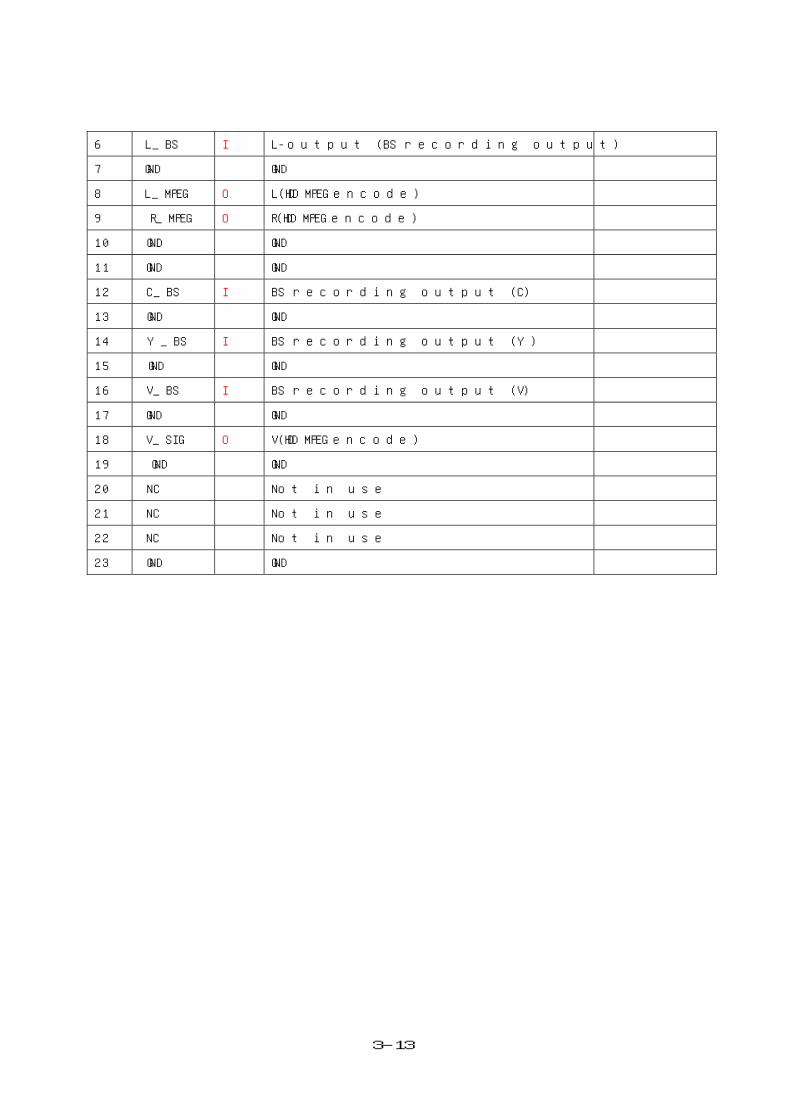
3-13
6 L_BS I L-output (BS recording output)
7 GND GND
8 L_MPEG O L(HDD MPEG encode)
9 R_MPEG O R(HDD MPEG encode)
10 GND GND
11 GND GND
12 C_BS I BS recording output (C)
13 GND GND
14 Y_BS I BS recording output (Y)
15 GND GND
16 V_BS I BS recording output (V)
17 GND GND
18 V_SIG O V(HDD MPEG encode)
19 GND GND
20 NC Not in use
21 NC Not in use
22 NC Not in use
23 GND GND
4-1
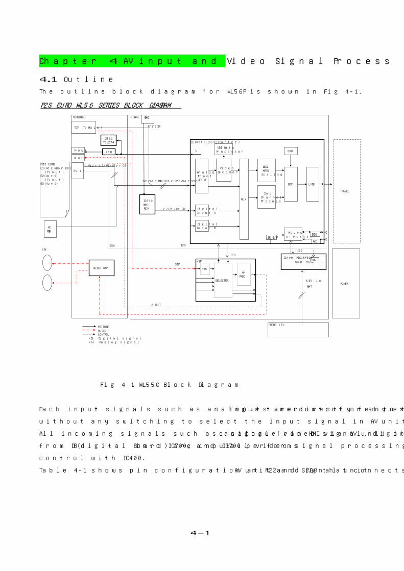
Chapter 4 AV input and Video Signal Process
4.1 Outline
The outline block diagram for WL56P is shown in Fig 4-1.
P2S EURO WL56 SERIES BLOCK DIAGRAM
PICTUREAUDIOCONTROL
(D) Digital signal(A) Analog signal
TERMINAL SIGNAL
OSD
HDMI
AV-in
AUDIO AMP
I2S
MSP
MTS
SELECTER
A-PROC
A.OUT
PANEL
V
Sub MICRO
POWER
75Ω
SIF
IC700:FLI8532(Cortez)
AnalogFrontEnd
VideoDecoder
MUX
VBI DataProcessor
DCDiMADi
Scaling
BEP LVDS
Micro-processorIR I/F
ADC
GPIO
DigitalInput A
DigitalInput B
2ndChannelProcess
TV/V1orRGB/V2orS2/V3orS3/PC
V1orYC/V2/V3orCS
ADC
I2S
I2S
Y/Cb/Cr(D)
IC400:PIC16F819
IC300HDMIRCV
R/G/B(D)
SPK
V-out
TIF (TV Main)
A-out
SSW
FRONT KEY
KEY in
RMT
PH2S EUROE1(VorRGBorTXT) (TV out)E2(VorS) (TV out)E3(VorS)
PCRGB
Q501TB1274
Fig 4-1 WL55C Block Diagram
Each input signals such as analogue tuner output or any external inputs are directly fed to the Signal unit via AV unit
without any switching to select the input signal in AV unit.
All incoming signals such as analogue video signal, digital video signal from HDMI via AV unit or digital video signal
from DB(digital Board) are input into IC700, and IC700 performs all video signal processing including the switching
control with IC400.
Table 4-1 shows pin configuration at PJ22 and PJ60 that connects AV unit and Signal unit
4-2
PJ22 PJ60
Pin# Signal Function Pin# Signal Function 50 A1 PC BLUE 50 GP7 TXT SW (TXT model only)
49 GND GND 49 GP8 Not in use
48 SV1 SCART 1 composite video signal 48 NC Not in use
47 GND GND 47 NC Not in use
46 C1 SCART 1 Blue 46 NC Not in use
45 GND GND 45 STOP_FAN
44 B1 SCART 2 C signal 44 SW_DVI2
43 GND GND 43 SW_DVI1
42 AN(RET) GND 42 NC
41 SV2 Not in use 41 GP9 PC Horizontal sync input
40 GND Not in use 40 GP10 PC Vertical sync input
39 A2 SCART 1 composite video signal 39 GP11 SCART 2 SLOW SWITCHING
38 GND GND 38 PDP_CONT
37 B2 SCART1 Green 37 PDP_MUTE
36 GND GND 36 NC
35 C2 PC GREEN 35 TV_MUTE
34 GND GND 34 EXT_MUTE
33 BN(RET) GND 33 MUTE
32 SV3 SCART 1 FAST BLANKING 32 R_HDMI
31 GND GND 31 L_HDMI
30 A3 SCART 1 RED 30 GND
29 GND GND 29 R_BS
28 B3 VIDEO3(S-video) C signal 28 L_BS
27 GND GND 27 GND
26 C3 TV composite video signal 26 R_TV
25 GND GND 25 L_TV
24 CN(RET) GND 24 GND
23 SV4 VIDEO3 composite video signal 23 W_APRO
22 GND GND 22 R_APRO
21 A4 VIDEO3(S-video) Y signal 21 L_APRO
20 GND GND 20 GND
19 B4 PC RED 19 R_MONITOR
18 GND GND 18 L_MONITOR
17 C4 SCART 2 (S-video) Y signal 17 GND
16 GND GND 16 R_E4
15 SVN(RET) GND 15 L_E4
14 V_BS Not in use 14 GND
13 V_BS_GND Not in use 13 R_E3
12 Y_BS Not in use 12 L_E3
11 C_BS Not in use 11 GND
10 GND GND 10 R_E2
9 MOUT IC700 Monitor output video signal 9 L_E2
8 GP1 Not in use 8 GND
7 GP2 Not in use 7 R_E1
6 GP3 AFT 6 L_E1
5 GP4 Not in use 5 GND
4 GP5 Video-3 S-video detection 4 SIF
3 GP6 SCART 1 SLOW SWITCHING 3 GND
2 SDA1 SDA1 2 SYS_SW2
1 SCL1 SCL1 1 SYS_SW1
Table 4-1 Pin configuration at connectors PJ22/PJ60

4-3
4.2 Circuitry
(1) Input/Output connection
Fig4-2 shows AV input/output block diagram on AV unit for 32/37WL56P.
The AV unit for 27WL56P is the same as except Video-2 terminal is fitted on Front AV unit.
AV BOARD SIGNAL BOARD PJ22
IC700UV TUNER V 26 C3
信号切り替えA/D変換
SCART 1 V 48 SV1 3D-YCSR 30 A3 Color DecoderG 37 B2 ScalerB 46 C1 画質制御FB 32 SV3 LVDS
その他
SCART 2 V/Y 17 C4C 44 B1
VIDEO3 V 23 SV4Y 21 A4C 28 B3
PC R 19 B4G 35 C2B 50 A1HV
MONITOR OUTV 9 MOUT
PJ60
41 GP940 GP10
Digital input port A
HDMI
HDMI DECODER
Fig 5-2 AV input/output block
TV tuner video signal, external input video signals ( Composite/S-video/SCART RGB(R/G/B/FB)), PC input
signal(R/G/B/H/V) are fed into IC700 on the signal unit through PJ22/PJ60, HDMI signal is directly fed into IC700
with digital signal conversion through HDMI receiver in Signal unit. The digital video signal from DB (Digital Board) is
directly fed into IC700.
IC700 performs the video signal process such as A/D convert, 3DYCS process, color decoding, scaling process and
picture controlling accordingly with input signal format.
IC700 outputs the monitor video output signal to QV16 that is a 75 ohm driver on AV unit through PJ22.
The monitor output signal is fed out from the monitor output terminal while the input signal is either composite
video signal or S-video signal only. When the input signal is either component signal, PC input or HDMI signal, the
monitor output is muted.
Signal selection
A/D converter
3DYCS
Colour Decoder
Scaler
Picture control
LVDS
Others
4-4
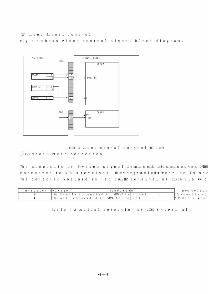
(2) Video Signal control
Fig 4-3 shows video control signal block diagram.
AV BOARD SIGNAL BOARD
IC700
SCART 1 8 316 32 SV3, M1
SCART 2 816
VIDEO3 S 4 M2
IC400RA1
39 RA0
PJ60
PJ22
FIG4-3 Video signal control Block
(1) Video1 S-Video detection
The composite or S-video signal input is accepted at VIDEO3 terminal and it is controlled whether S cable is
connected to VIDEO-3 terminal. The logical detection is shown in the table 4-2.
The detected voltage is fed to M2 terminal of IC700 via #4 of PJ22.
Detection voltage Condition IC700 selection
H No S cable connected to VIDEO-3 terminal Composite video signal
L S cable connected to VIDEO-3 terminal S-Video signal
Table 4-2 Logical detection at VIDEO-3 terminal
4-5
(2) SCART 1, 2 SLOW SWITCHING Control
When any external equipments connected either SCART 1 or SCART 2 terminal are turned on while viewing TV
program, the input is automatically set to either SCART 1 or SCART 2 by detecting the voltage at #8 of SCART
terminal. The picture size is also set automatically according to the output of the equipment. The detected
voltage is fed to IC400 on Signal unit through PJ22/PJ60 and IC400 controls IC700 to select signal switching
and picture size.
The SLOW SWITCHING control is in common control for SCART 1 and SCART 2 but the priority is set to the
condition changed lastly. (Last Memory function)
Detected voltage Condition IC700 Control
H The picture not in 4 by 3 format at SCART Select SCART input and set picture size
as last memory
M The Picture in 4 by 3 format at SCART Select SCART input and set picture size
as 4 by 3.
L No Picture at SCART No control
Table 4-3 Logical function of SCART SLOW SWITCHING
(3) SCART1 FAST BLANKING Control
SCART 1 adopts to receive the composite video signal or RGB video signal. To select those is performed by
detecting the voltage at pin 16 (FAST BLANKING) of SCART 1 terminal.
The detected voltage is fed to pin M1 of IC700 through PJ22 and IC700 controls the input signal as shown in
table 4-4.
In case of TOGGLE mode, the picture may appear like RGB picture superimposed on the composite video
picture.
FFLASH BLANKING is available on SCART-1 only.
Detected Voltage Condiiiton IC700 Control
H RGB signal input to SCART 1 Switch to RGB input
L Composite video signal input to SCART 1 Switch to composite video input
TOGGLE Superimposed video signal input to SCART 1 Switch to composite at L
Switch to RGB input at H
Table 4-4 Logical FAST BLANKING control
5-1
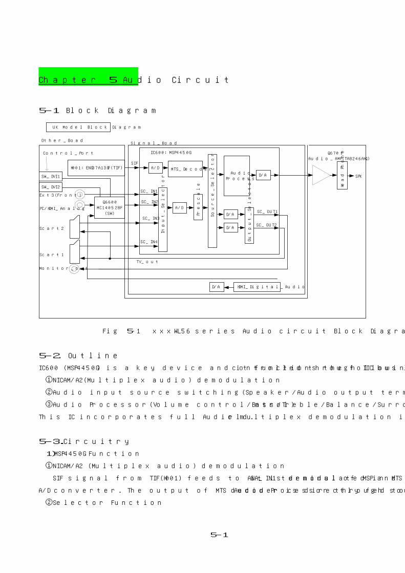
Chapter 5 Audio Circuit
5-1 Block Diagram
H001:ENG37A13GF(TIF)
Q6600MC14052BF
(SW)PC/HDMI_Analog
Ext3(Front)
Monitor_out
Signal_Boad
Q670:Audio_AMP(TA8246AHQ)
Head
Pho
ne
SPK
Other_Boad
UK Model Block Diagram
Scart1
Scart2
TV_out
AudioProcessor
Sour
ce_
Sel
ecto
r
MTS_Decoder
IC600:MSP4450G
SIFIn
put_
Sel
ecto
r A/D
Pre
scal
e
D/A
D/A
Out
put_
Sele
cto
r
A/D
D/A
HDMI_Digital_Audio
SC_IN1
SC_IN2
SC_IN3
SC_OUT1
SC_OUT2
SC_IN4
D/A
SW_DVI1
Control_Port
SW_DVI2
Fig 5-1 xxxWL56 series Audio circuit Block Diagram
5-2. Outline
IC600 (MSP4450G) is a key device and it functions the following controlled through IIC bus line.
①NICAM/A2(Multiplex audio) demodulation
②Audio input source switching(Speaker/Audio output terminal)
③Audio Processor(Volume control/Bass/Treble/Balance/Surround control)
This IC incorporates full Audio multiplex demodulation in the world.
5-3.Circuitry
1)MSP4450G Function
①NICAM/A2 (Multiplex audio) demodulation
SIF signal from TIF(H001) feeds to ANA_IN1 terminal of MSP and it is demodulated in MTS decoder after
A/D converter. The output of MTS decoder is directly fed to the Audio Processor through source selector.
②Selector Function
5-2
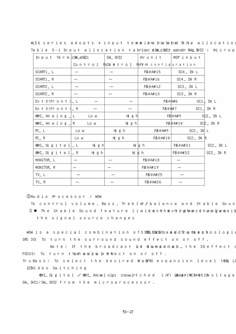
WL56 series adopts 4 input terminals and the allocation is shown in table 5-1.
Table 5-1 Input allocation table (SW_DVI1 and SW_DVI2 : Microprocessor ports)
Input Terminal
SW_DVI1
Control Port
SW_DVI2
Control Port
AV unit
Pin configuration
MSP input
SCART1_L - - PJ60A#15 SC4_IN L
SCART1_R - - PJ60A#16 SC4_IN R
SCART2_L - - PJ60A#12 SC3_IN L
SCART2_R - - PJ60A#13 SC3_IN R
Ext3(Front)_L - - PJ60A#6 SC1_IN L
Ext3(Front)_R - - PJ60A#7 SC1_IN R
HDMI_Analog_L Low High PJ60A#9 SC2_IN L
HDMI_Analog_R Low High PJ60A#10 SC2_IN R
PC_L Low High PJ60A#9 SC2_IN L
PC_R Low High PJ60A#10 SC2_IN R
HDMI_Digital_L High High PJ60A#31 SC2_IN L
HDMI_Digital_R High High PJ60A#32 SC2_IN R
MONITOR_L - - PJ60A#18 -
MONITOR_R - - PJ60A#19 -
TV_L - - PJ60A#25 -
TV_R - - PJ60A#26 -
③Audio Processor / WOW
To control volume, Bass, Treble, balance and Stable Sound On/Off.
The Stable Sound feature limits the highest volume level to prevent extreme changes in volume when
the signal source changes
WOW is a special combination of SRS Labs audio technologies (SRS 3D,FOCUS and TruBass).
SRS 3D: To turn the surround sound effect on or off.
Note: If the broadcast is monaural, the 3D effect does not function.
FOCUS: To turn the vocal emphasis effect on or off.
TruBass: To select the desired bass expansion level (HIGH, LOW or OFF)
2)Video Switching
HDMI_Digital / HDMI_Analog source is switched in Q6600(MC14052BF) by the voltage of
SW_DVI1/SW_DVI2 from the microprocessor.
5-3
5-4. Troubleshooting
1.No Sound from the speaker
No Sound Set the volume at 50 display
Output copper patter
open circuit or C681
and C682
Replace Q670
Check the waveform
at SPK terminal Check speaker OK
Check the waveforms at
#2,3 on P602?
Check the wiring to
the speaker
OK
Check the waveform
at #8,#12 of Q670 Check the waveform at (+)
of C660 and C661 OK
Check that DC voltage at (+) of
C660 and C661 is approx. 5.3V
Check the
waveform at
#11/#7 of IC602 OK
Check the waveform at
#20/21 of IC600
Check FCC fitting after IC600
OK
Check +5V and +9V line to Signal unit.
OK
Check Vcc at #9
of Q670
Check Vcc=+26V line
NG
NG
NG
NG
NG
NG
NG
OK
5-4
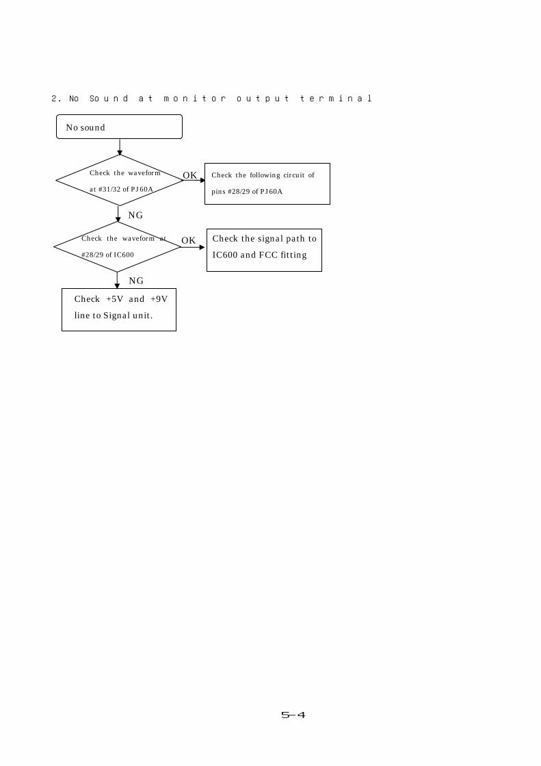
2. No Sound at monitor output terminal
No sound
Check the waveform
at #31/32 of PJ60A
Check the following circuit of
pins #28/29 of PJ60A OK
Check the waveform at
#28/29 of IC600
Check the signal path to IC600 and FCC fitting
OK
Check +5V and +9V
line to Signal unit.
NG
NG
6-1
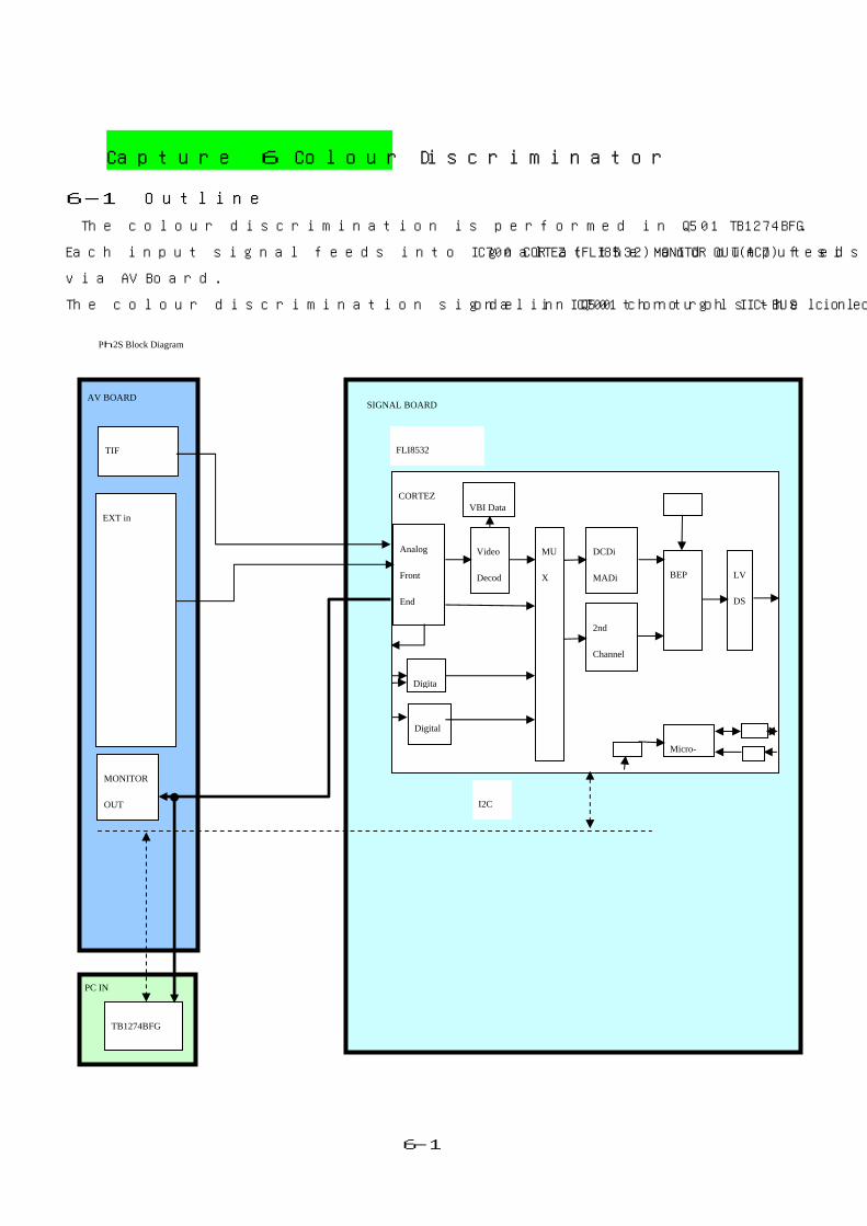
Capture 6 Colour Discriminator
6-1 Outline
The colour discrimination is performed in Q501 TB1274BFG.
Each input signal feeds into IC700 CORTEZ(FLI8532) and output signal at the MONITOR OUT(AC7) feeds into Q501
via AV Board.
The colour discrimination signal in Q501 controls the colour decode in IC700 through IIC-BUS line.
CORTEZ
Analog
Front
End
Video
Decod
MU
X
VBI Data
DCDi
MADi BEP LV
DS
Micro-
Digita
Digital
2nd
Channel
I2C
SIGNAL BOARD
FLI8532
PC IN
Ph2S Block Diagram
AV BOARD
TIF
EXT in
TB1274BFG
MONITOR
OUT
6-2
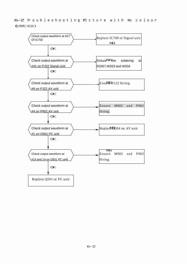
6-2 Troubleshooting:Picture with No colour
(EUROPE/ASIA)
NG
OK
NG
OK
NG
OK
NG
OK
NG
OK
NG
OK
Ensure the soldering at
R2057,W203 and W204
Replace IC700 or Signal unit
Ensure PJ22 fitting.
Check output waveform at AC7 Of IC700
Check output waveform at
#41 on PJ22 Signal Unit
Check output waveform at
#9 on PJ22 AV unit
Check output waveform at
#4 on P902 AV unit
Check output waveform at
#1 on Q501 PC unit
Ensure M902 and P902 fitting.
Replace Q504 on AV unit
Ensure M902 and P902 fitting.
Replace Q501 or PC unit
Check output waveform at
#13 and 14 on Q501 PC unit
7-1
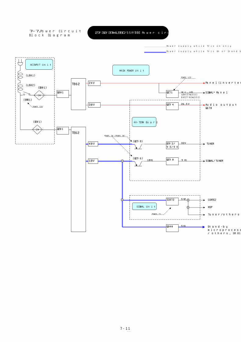
Chapter 7. Power Circuit
7-1 Outline
The power circuit is consisting of several blocks as shown in Block diagram. It is mainly consisting of AC
INPUT Unit, Main Power Unit, Sub-Power Unit and regulators for signal process.
①ACINPUTUnit
It is consisting of line filter (T801and T802), Reactors(L801 and L80), rectifying stuck diodes(D801 and
DE01), AC relay (SR81) and others to rectify the AC input.
②MAIN POWER Unit
It generates +24V for LCD panel and +30V for Audio output with using Q801(STR-Z4369).
While the stand-by mode, the MAIN POWER Unit is turned off by SR81 off.(Open)
③SUB-POWER Unit
It generates +40V, +18V, +6.5V1 and +6.5V2 for stand-by microprocessor, Signal Unit, Tuner and
others. New device STR-W6765 is employed as QE01.
④Regulator for Signal process
The Regulators QE71, QE40 and QE40 are located in the MAIN POWER Unit.
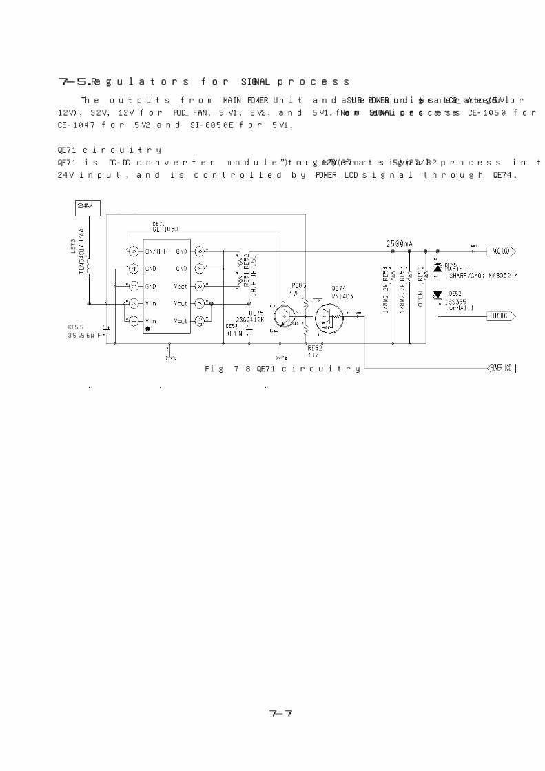
・ Regulator : QE71 (Device Name: CE-1050)
QE71 is DC-DC converter module to generate +5V(27/32”) or +12V(37”) that controls Signal
process in LCD Panel module at +24V input and it is controlled by POWER_LCD signal.
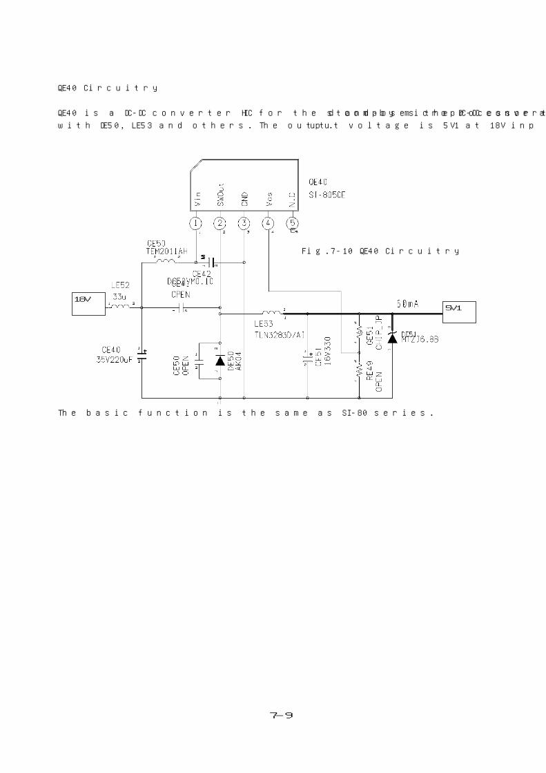
・ Regulator : QE40 (Device Name: SI-8050E)
QE40 is HIC to compose DC-DC Converter with DE50, LE53 and other components for stand-by
microprocessor. It outputs 5V1 at 18V input
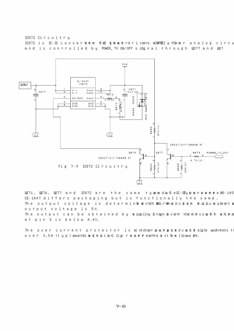
・ Regulator : IC872 (Device Name: CE-1047) located in Signal Unit
IC872 is DC-DC Converter module to generate 5V2 at 18V input for CPRTEZ, TUNER and other
analog circuit and it is controlled by POWER_TV signal.
Power Line control
Main power lines (+24V and +30V) is off when the power SW is turned off or in stand-by mode due to
SR81 open circuit controlled by POWER_SIG OFF signal.
The SUB-Power Line through DE01 remains the output while Stand-by mode.
7-2
7-2.AC INPUT Unit
AC input is rectified through AC INPUT Unit. D899 is a varistor and absolves the surge current on AC line.
It protects the circuit bypassing the surge current as shown below. C801, C802, T801, T802, C811, C812,
CE13 and CE14 compose the filtering circuit to eliminate the unnecessary noises. D801 is a bridge rectifier to
generate main power with C810 and C8100 for the Main power source. DE01 with CE10 generates Sub Power
source.
The Coke coils L801 and L802 suppress the AC line noises and harmonic wave noise.
FIG 7-1 AC INPUT Unit
POWER_SIG
SR81
DE01
CE10
L802
D801
C810 ,C8100
F801 D899
C801
C811 C812
C802
T801
Main Power output
5V1
Secondary
GND
Surge
+
+
Sub –Power output
L801
D852
Q851
Q852
CE13
CE14
Secondary GND
7-3
7-3.MAIN POWER Unit
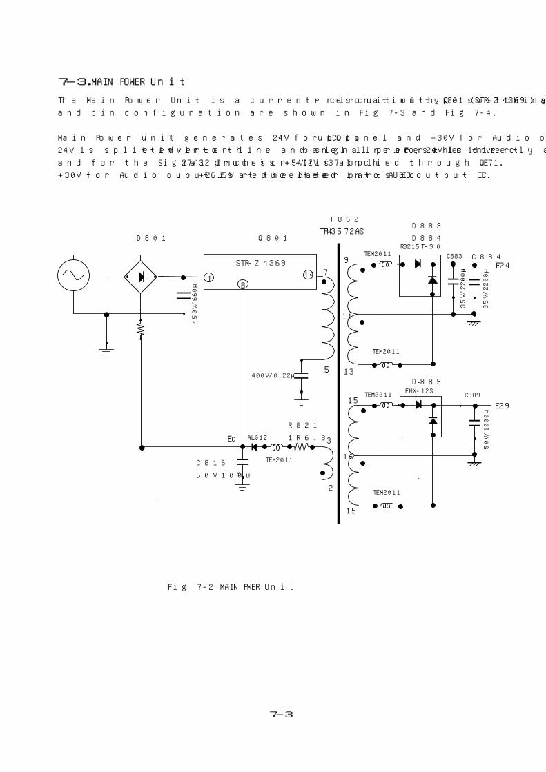
The Main Power Unit is a current- resonation type switching power circuit with Q801 (STR-Z4369) and IC block
and pin configuration are shown in Fig 7-3 and Fig 7-4.
Main Power unit generates 24V for LCD panel and +30V for Audio ouput.
24V is splitted into the inverter line and signal process in the panel line. For the inverter, 24V is direcly applied
and for the Signal process +5V (27/32 Inch ) or +12V (37 Inch ) is applied through QE71.
+30V for Audio ouput is reduced to +26.5V at the later parts to feed into AUDIO output IC.
Fig 7-2 MAIN PWER Unit
TPW3572AS
450V
/660
μ
7
5
3
2
1 14
STR-Z4369
13
9
11
AL01Z 1R68
E24C883
16
RB215T-90
Ed
C81550V/100μ
TEM2011
8
400V/0.22μ
35V
/220
0μ
TEM2011
TEM2011
35V
/220
0μ
15
50V
/100
0μ
15
TEM2011
TEM2011 C889
E29
FMX-12S
D801 Q801
T862D883
D884
C884
D885
C816
50V100u
R821
1R6.8
7-4
Pin # Signal Function
1 VIN Half bridge power in
3 GND GND for controlling
4 CONT Controls oscillator
5 Css For soft start-up capacitor connection
6 CD For delayed latch capacitor connection
7 DT For dead-time setting resistor connection
8 Vcc Power for control
9 DRI Vcc Power output for gate drive circuit
10 OC To detect over current
11 RC To detect resonated current
12 COM Half bridge GND
14 OUT Half bridge output
15 VB Power input for high-side Gate drive circuit
Fig7-3 STR-Z4369 Block Diagram
Fig 7-4 STR-Z4369 Pin Configuration
7-5
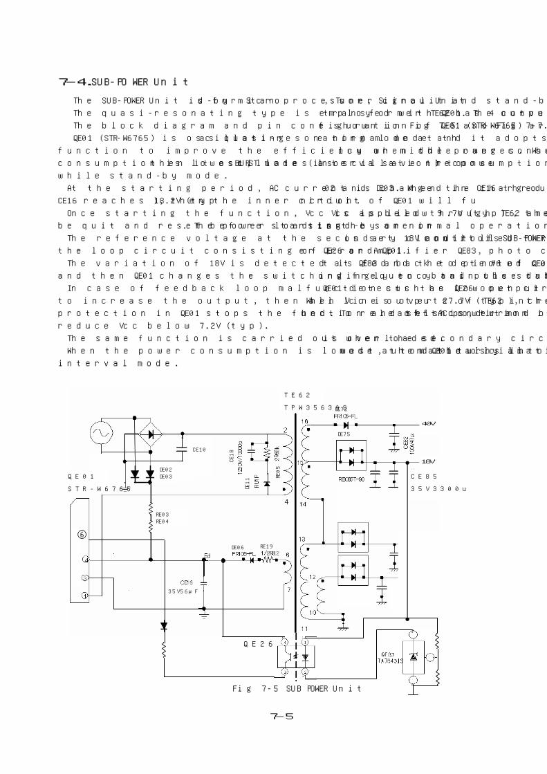
7-4.SUB-POWER Unit
The SUB-POWER Unit is for Stand-by microprocessor, Signal Unit, Tuner circuit and stand-by power source.
The quasi-resonating type is employed with QE01. The converter transformer TE62 has 4 output lines.
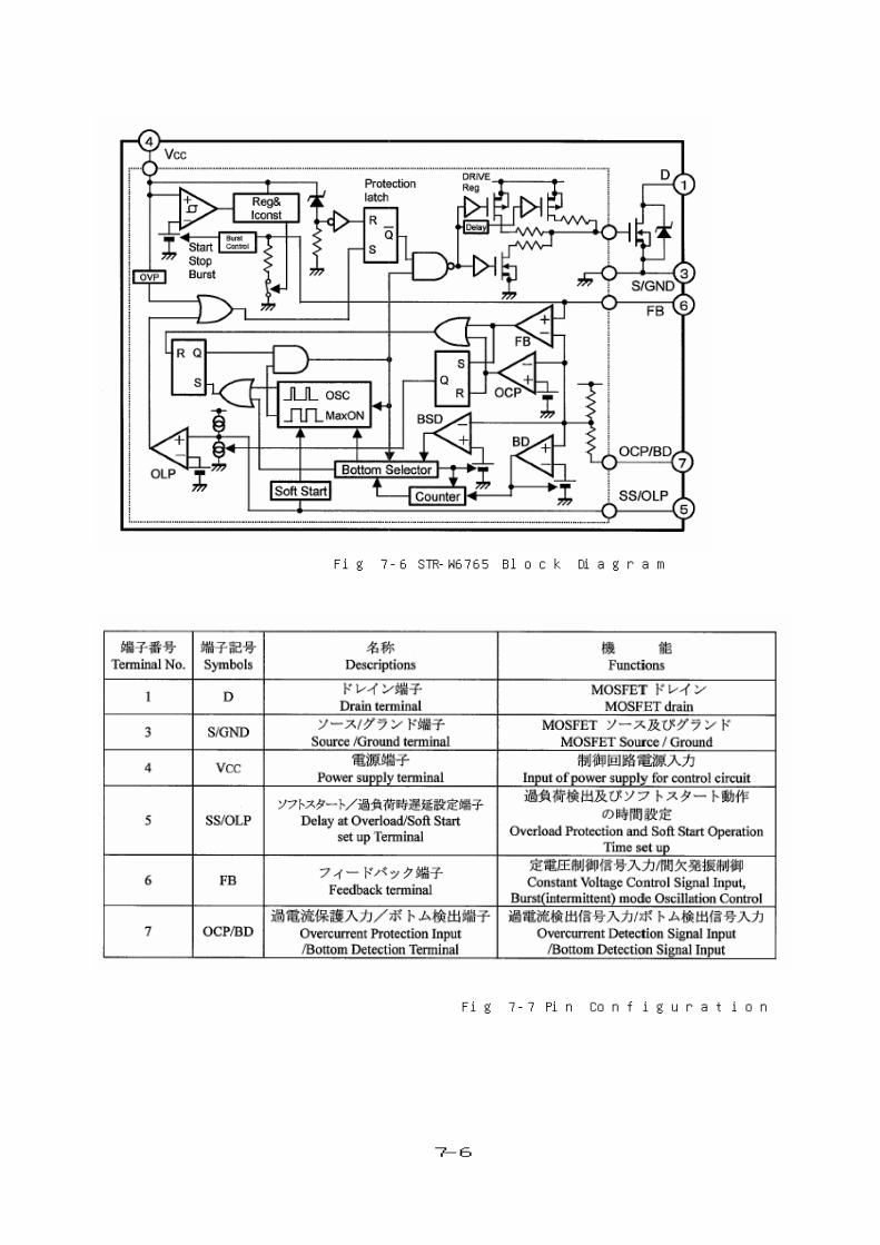
The block diagram and pin configuration of QE01 (STR-W6765) are shown in Fig 7-5 and Fig 7-7.
QE01 (STR-W6765) is oscillating as quasi-resonating mode at the normal mode and it adopts the bottom skip
function to improve the efficiency when the power consumption is low or middle ranges. When the power
consumption is lowest, then it oscillates as BURST mode (interval oscillation) to save the power consumption
while stand-by mode.
At the starting period, AC current is charged in CE16 through DE02 and DE03. When the charged voltage at
CE16 reaches 18.2V (typ), then the inner circuit of QE01 will function.
Once starting the function, Vcc is applied through TE62 and when Vcc is below 9.7V (typ) , the function will
be quit and reset before starting. The power load is the same in stand-by or normal operation mode.
The reference voltage at the secondary circuit of SUB-POWER Unit is set 18V and it is controlled through
the loop circuit consisting of Error Amplifier QE83, photo coupler QE26 and QE01.
The variation of 18V is detected at QE83 and the detected current is fed back to pin#6 of QE01 though QE26
and then QE01 changes the switching frequency and pulse duty accordingly to obtain the stable 18V.
In case of feedback loop malfunction such as QE26 open circuit, QE01 detects the low output and functions
to increase the output, then all line outputs of TE62 increase. When Vcc is over 27.7V (typ), the over voltage
protection in QE01 stops the function and this condition is latched. To release this, turn off AC power and on to
reduce Vcc below 7.2V (typ).
The same function is carried out when the secondary circuit load is overloaded.
When the power consumption is lowest, then QE01 turns into BURST mode automatically and the oscillation is
interval mode.
Fig 7-5 SUB POWER Unit
QE01STR-W6756
TE62
35V56μF
DE06 RE19
DE11
CE18
RE05
DE72
DE75
DE73
DE77
40V
18V
6.5V1
6.5V2
DE02DE03
RE03RE04
CE10
QE26
⑥
CE85
35V3300u
TE62
TPW3563AS
QE01
STR-W6765
7-6
Fig 7-6 STR-W6765 Block Diagram
Fig 7-7 Pin Configuration
7-7
7-5.Regulators for SIGNAL process
The outputs from MAIN POWER Unit and SUB POWER Unit are regulated and generated as LCD_Vcc(5V or
12V), 32V, 12V for POD_FAN, 9V1, 5V2, and 5V1 for SIGNAL process. New Devices are CE-1050 for LCD_Vcc,
CE-1047 for 5V2 and SI-8050E for 5V1.
QE71 circuitry
QE71 is DC-DC converter module to generate 5V(27/32”) or 12V(37”) for signal process in the LCD panel at
24V input, and is controlled by POWER_LCD signal through QE74.
CE55 35V56μF
LE
73
24V
Fig 7-8 QE71 circuitry
7-8
IC872 Circuitry
IC872 is DC-DC converter to generate 5V2 that drives CORTEZ, Tuner and other analog circuits at 18V input
and is controlled by POWER_TV ON/OFF signal through Q877 and Q878.
QE71, QE76, QE77 and IC872 are the same type of DC-DC converter module. Type name CE-1050 or
CE-1047 differs packaging but is functionally the same.
The output voltage is determined the resistor value between pin 8 and GND. When pin 8 is open circuit, the
output voltage is 5V.
The output can be obtained by applying over 3V or open circuit at pin 5 and it turns off when the applied voltage
at pin 5 is below 0.4V.
The over current protector is incorporated and it works to reduce the output voltage when the load current is
over 3.5A (typ) and also it is automatically reset when the load current is below 1A.
18V
Fig 7-9 IC872 Circuitry
7-9
QE40 Circuitry
QE40 is a DC-DC converter HIC for the stand-by microprocessor and composes the DC-DC converter circuit
with DE50, LE53 and others. The output voltage is 5V1 at 18V input.
The basic function is the same as SI-80 series.
18V5V1
Fig.7-10 QE40 Circuitry
7-10
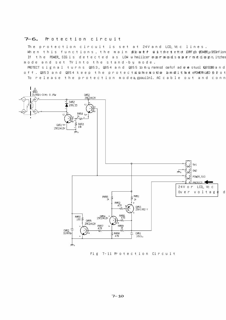
7-6. Protection circuit
The protection circuit is set at 24V and LCD_Vcc lines.
When this functions, the main power is set to OFF by turning SR-81 off with setting POWER_SIG forced LOW.
If the POWER_SIG is detected as LOW while normal operation, the microprocessor recognizes the protection
mode and set TV into the stand-by mode.
PROTECT signal turns Q853, Q854 and Q855 on, and as a result SR81 turns off due to Q851 and Q852 turns
off. Q853 and Q854 keep the protection mode and the POWER LED flashes to indicate the protection mode.
To release the protection mode, pull AC cable out and connect it again.
Fig 7-11 Protection Circuit
24VorLCD_Vccの過電圧検出回路
24V or LCD_Vcc
Over voltage detection
Power supply while TV is on only
Power supply while TV is On or Stand by
26.5V
32V
18V1 9V1
5V2
5V1
7-11
24V Panel(inverter)
SIGNAL→PanelQ801
QE01
30V
T862
TE62
QE71
Stand-bymicroprocessor/ others, SR 81
(SR81)
DE92/93/94
(D801)
Audio outputQ670
TUNER
CORTEZ
MSP
SIGNAL/TUNERQE90
40V
18V
(DE01)
(L801)
IC872
Q840
(L802)
QE94
Vcc_LCD12V(37WL55C)5V(27・32WL55C)
(QE98)
(QE96)
Tuner/others
27/32/37WL55C/55P/55E Power circuit Block
MAIN POWER Unit
SIGNAL Unit
POWER_LCD
POWER_SIG
POWER_SW (POWER_DB)
POWER_TV
AV-TERM Board
ACINPUT Unit
7-7.Power CircuitBlock Diagram
7-11
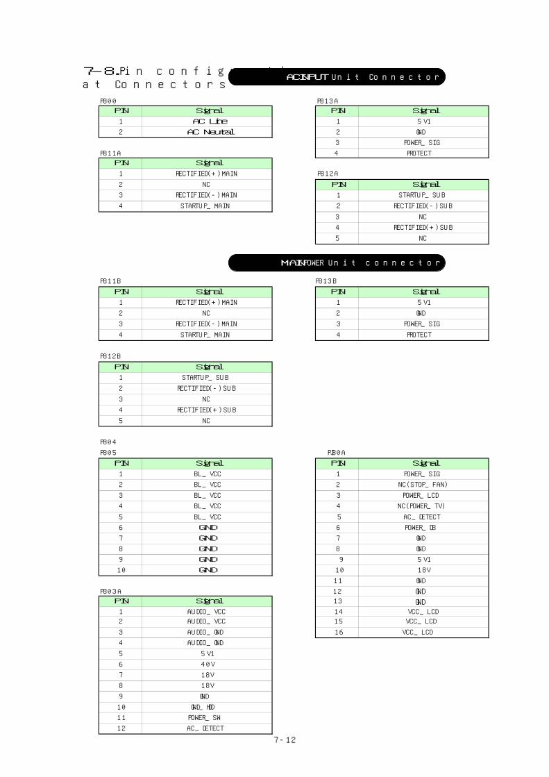
P800 P813APIN PIN
1 1
2 2
3
P811A 4PIN
1 P812A
2 PIN
3 1
4 2
3
4
5
P811B P813B
PIN PIN
1 1
2 2
3 3
4 4
P812B
PIN
1
2
3
4
5
P804
P805 PJ80A
PIN PIN
1 1
2 2
3 3
4 4
5 5
6 6
7 7
8 8
9 9
10 10
11
P803A 12PIN 13
1 142 15
3 16
4
5
6
7
8
9
10
11
12
7-12
18V
GND
18V
RECTIFIED(-)SUB
RECTIFIED(+)SUB
AC_DETECT
POWER_SW
GND_HDD
5V1
40V
AUDIO_GND VCC_LCD
AUDIO_VCC
AUDIO_GND
VCC_LCDAUDIO_VCC VCC_LCD
GND
GND
BL_VCC
GND
BL_VCC
BL_VCC
GND
GND
GND
NC(POWER_TV)
POWER_LCD
POWER_SIG
Signal
BL_VCC
NC(STOP_FAN)
GND
Signal
5V1
18V
GND
AC_DETECT
POWER_DB
GND
NC
RECTIFIED(+)SUB
NC
RECTIFIED(-)MAIN
STARTUP_MAIN
Signal
RECTIFIED(-)MAIN
STARTUP_MAIN
Signal
AC Line
RECTIFIED(+)MAIN
AC Neutral
NC
RECTIFIED(+)MAIN
NC
STARTUP_SUB
Signal
GND
NC
Signal
Signal
NC
BL_VCC
Signal
5V1
GND
POWER_SIG
PROTECT
Signal
STARTUP_SUB
RECTIFIED(-)SUB
GND
POWER_SIG
PROTECT
Signal
5V1
ACINPUTボードコネクタ仕様7-8.Pin configurationat Connectors
ACINPUT Unit Connector
MAINPOWER Unit connector
7-13
POWER_DB(POWER_SW)
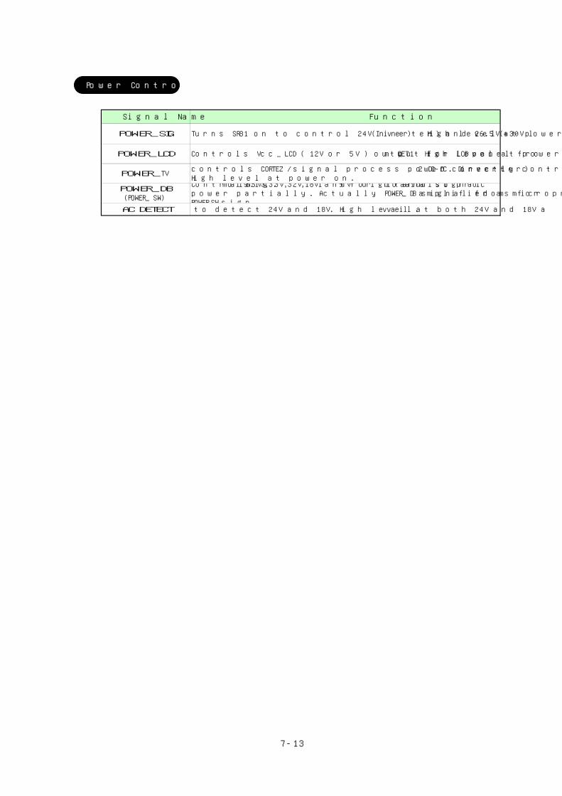
Controls mainly 6.5V3, 3.3V, 32V, 18V1 and 9V for digital board and also signal processpower partially. Actually POWER_DB signal from microprocessor is amplified as forPOWER SW signal
AC DETECT to detect 24V and 18V. High level at both 24V and 18V avail.
Signal Name Function
POWER_SIG Turns SR81 on to control 24V(Inverter) and 26.5V(+30V line) High level at power on.
POWER_LCD Controls Vcc_LCD ( 12V or 5V ) output for LCD panel from QE71 High level at power on.
POWER_TVcontrols CORTEZ/signal process power. Directly controls IC872(5V2 DC-DC converter)High level at power on.
Power Control Signal
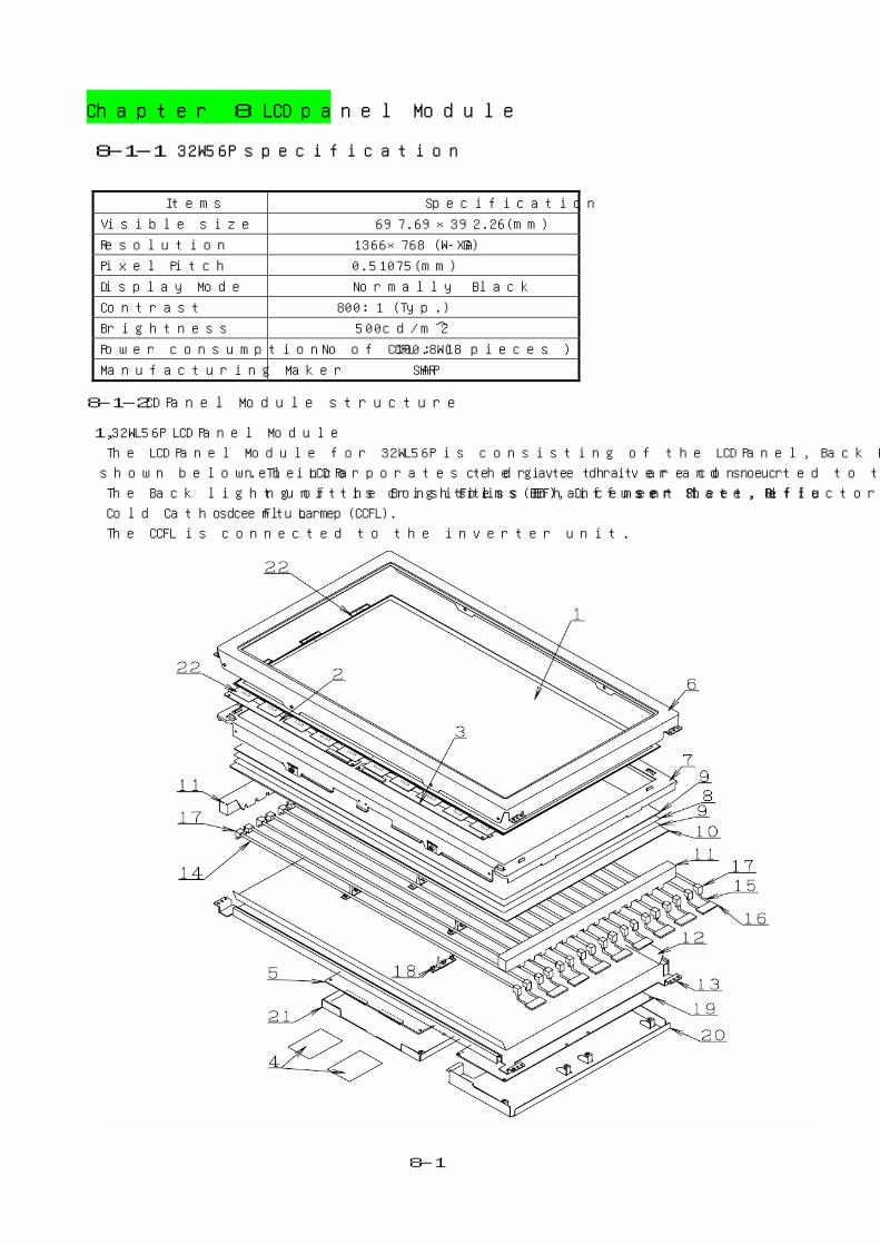
8-1
Chapter 8 LCD panel Module
8-1-1 32W56P specification
Items Specification
Visible size 697.69×392.26(mm)
Resolution 1366×768 (W-XGA)
Pixel Pitch 0.51075(mm)
Display Mode Normally Black
Contrast 800:1 (Typ.)
Brightness 500cd/m^2
Power consumption 100.8W( No of CCFL : 18 pieces )
Manufacturing Maker SHARP
8-1-2CD Panel Module structure
1,32WL56P LCD Panel Module
The LCD Panel Module for 32WL56P is consisting of the LCD Panel, Back Light unit, the inverter unit and the drive unit as
shown below. The LCD Panel incorporates the gate driver and source drive that are connected to the drive unit through FPC.
The Back light unit is consisting of the Brightness Enhancement Films(BEF), Diffuser Sheet, Diffuser Plate, Reflector and the
Cold Cathode Fluorescent Lamp(CCFL).
The CCFL is connected to the inverter unit.
8-2
2.Connection
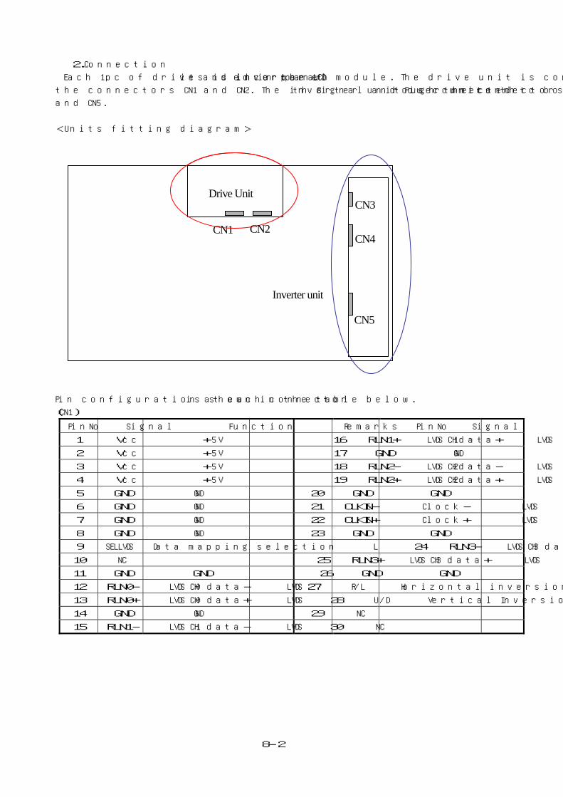
Each 1pc of drive and inverter units is incorporated in the LCD panel module. The drive unit is connected to Signal unit through
the connectors CN1 and CN2. The inverter unit is connected to both Signal and Power units through the connectors CN3, CN4
and CN5.
<Units fitting diagram>
Pin configuration at each connector is shown in the table below.
(CN1)
PinNo Signal Function Remarks PinNo Signal Function Remarks
1 Vcc +5V 16 RLN1+ LVDS CH1data+ LVDS
2 Vcc +5V 17 GND GND
3 Vcc +5V 18 RLN2- LVDS CH2data- LVDS
4 Vcc +5V 19 RLN2+ LVDS CH2data+ LVDS
5 GND GND 20 GND GND
6 GND GND 21 CLKIN- Clock- LVDS
7 GND GND 22 CLKIN+ Clock+ LVDS
8 GND GND 23 GND GND
9 SELLVDS Data mapping selection L 24 RLN3- LVDS CH3 data- LVDS
10 NC 25 RLN3+ LVDS CH3 data+ LVDS
11 GND GND 26 GND GND
12 RLN0- LVDS CH0 data- LVDS 27 R/L Horizontal inversion
13 RLN0+ LVDS CH0 data+ LVDS 28 U/D Vertical Inversion
14 GND GND 29 NC
15 RLN1- LVDS CH1 data- LVDS 30 NC
CN1
ドライブ基板
CN3
インバータ基板 スタ側
インバータ基板スレーブ側
CN2
CN1
Drive Unit
CN5
Inverter unit
CN2 CN4
CN3
8-3
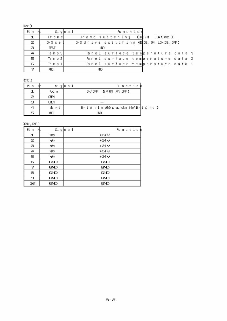
(CN2)
Pin No Signal Function
1 Frame Frame switching (HIGH:60Hz LOW:50Hz)
2 O/S set O/S drive switching(HIGH:OS_ON LOW:OS_OFF)
3 TEST GND
4 Temp3 Panel surface temperature data 3
5 Temp2 Panel surface temperature data 2
6 Temp1 Panel surface temperature data 1
7 GND GND
(CN3)
Pin No Signal Function
1 Von ON/OFF (5V:ON 0V:OFF)
2 OPEN -
3 OPEN -
4 Vbrt Brightness control (5V:dark 0V:Bright)
5 GND GND
(CN4,CN5)
Pin No Signal Function
1 VINV +24V
2 VINV +24V
3 VINV +24V
4 VINV +24V
5 VINV +24V
6 GND GND
7 GND GND
8 GND GND
9 GND GND
10 GND GND
8-4
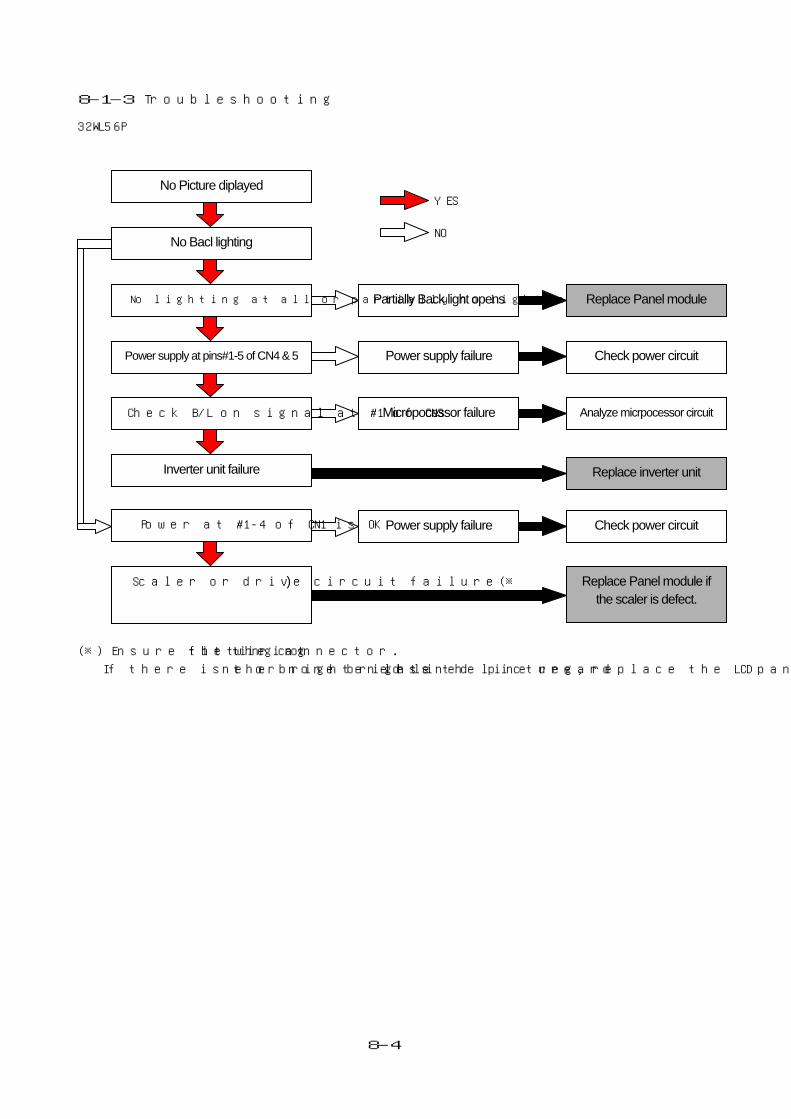
8-1-3 Troubleshooting
32WL56P
(※) Ensure the wiring fitting at the connector.
If there is the brightened line or none brightened line regardless the picture, replace the LCD panel module.
No Bacl lighting
No lighting at all or partially no lighting
Power supply at pins#1-5 of CN4 & 5
Check B/L on signal at #1 of CN3
No Picture diplayed
Inverter unit failure
Scaler or drive circuit failure(※)
Partially Back light opens
Power supply failure
Micropocessor failure
Replace inverter unit
Replace Panel module if the scaler is defect.
Replace Panel module
Check power circuit
Analyze micrpocessor circuit
YES
NO
Power at #1-4 of CN1 is OK Power supply failure Check power circuit
8-5
8-1-4 HANDLING THE LCD MODULE
Safety Precautions
In the event that the screen is damaged or the liquid crystal (fluid) leaks, Do not breath in or drink it. Also, never touch the fluid.
Such actions could cause toxicity or skin irritation. If the fluid should enter the mouth, rinse the mouth thoroughly with water. If the
fluid should contact the skin or clothing, wipe off with alcohol, etc., and rinse thoroughly with water. If the fluid should enter the eyes,
rinse the eyes immediately thoroughly with running water, and consult the doctor.
Precautions for handling the LCD module
The LCD module can easily be damaged during dismantling or reassembling, therefore, observe the following precautions while
handling the LCD module.
1. When fitting the LCD module to the LCD cover, position it appropriately and fix it in the position where the display can be
viewed most conveniently.
2. Align the holes at each corners of the LCD module carefully to the corresponding holes on the LCD cover and fix with screws.
Do not push the LCD module with excessive forces to avoid any possible improper performance due to the excessive impact
to the module.
Be careful with handling the polarized screen because it can be easily damaged.
3. In case of the panel surface soiled, wipe with the cotton or a soft cloth. The soiling is still remained, breath on the surface and
then wipe off. In case the panel surface soiled extremely, wipe off the panel surface with CRT cleaner dropping to the cloth.
Do not drop the CRT cleaner directly to the panel surface.
4. Leaving water or other fluids on the panel surface for a long time can easily cause the discoloration or stripes on the surface.
Wipe off immediately the surface.
5. Do not drop or hit with hard objects the panel to avoid any damages on the glass used in the LCD module.
6. Avoid any static electric shocks to the LCD module due to COMOS-LSI incorporated in.
7. Do not expose the LCD module under the direct sunlight or any strong ultraviolet rays for a long time.
8. Do not store the LCD module below the temperature specified to avoid any possible damages such as a bending, freezing the
liquid crystal or others.
9. Do not dismantle the LCD module itself to avoid any possible damages.
10. Do not pack the LCD module with any packing materials containing epoxy resin (amine) or silicon resin (Alcohol, oxim) to avoid
any polarity loss due to the gas generated from them.
Precaution for the LCD module response
1. Display response timing may vary the using temperature. When the temperature is low, the display response may be slower.
2. The brightness or the colour uniformity may change due to the temperature.
3. The condensation due to dew may occur if the LCD module is used in the sudden temperature changed circumstances and
may cause malfunctions.
4. Do not fit or disconnect any wirings with power On condition to avoid any possible malfunction.
Precaution for the static electric shocks to the LCD module
1. Do not touch directly to any connectors without any preparation not to apply any static electric shock to the LCD module.
2. Pull slowly the protection sheet on the surface of the LCD module off to avoid any possible static electric shocks to the LCD
module.
Precaution for the storing the LCD module
1. Keep it off from the direct sunlight or any ultraviolet light source.
2. Store it within the temperature between -5 ̃ 35 degree centigrade with less than RH60%.
3. Store it without any possible touching of any objects to the surface.
8-6
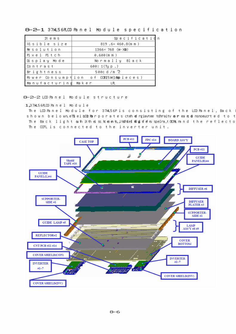
8-2-1 37WL56PLCD Panel Module specification
Items Specification
Visible size 819.6×460.8(mm)
Resolution 1366×768 (W-XGA)
Pixel Pitch 0.600(mm)
Display Mode Normally Black
Contrast 600:1(Typ.)
Brightness 500cd/m^2
Power Consumption 125W( No of CCFL :16pieces)
Manufacturing Maker LPL
8-2-2 LCD Panel Module structure
1,37WL56PLCD Panel Module
The LCD Panel Module for 37WL56P is consisting of the LCD Panel, Back Light unit, the inverter unit and the drive unit as
shown below. The LCD Panel incorporates the gate driver and source drive that are connected to the drive unit through FPC.
The Back light unit is consisting of the sheet, diffuser platter, the diffuser, CCFL and the reflector.
The CCFL is connected to the inverter unit.

8-7
2.Connection
1pc of drive unit and 2pcs of inverter units are incorporated in the LCD panel module. The drive unit is connected to Signal unit
through the connectors CN1. The inverter unit is connected to the Power units through the connectors CN2 and CN3.
<Units fitting diagram>
Pin configuration at each connector is shown in the table below
(CN1)
PinNo Signal Function Remarks PinNo Signal Function Remarks
1 Vcc +5V 16 RLN1+ LVDS CH1data+ LVDS
2 Vcc +5V 17 GND GND
3 Vcc +5V 18 RLN2- LVDS CH2data- LVDS
4 Vcc +5V 19 RLN2+ LVDS CH2data+ LVDS
5 GND GND 20 GND GND
6 GND GND 21 CLKIN- Clock- LVDS
7 GND GND 22 CLKIN+ Clock+ LVDS
8 GND GND 23 GND GND
9 SELLVDS Data mapping selection L 24 RLN3- LVDS CH3 data- LVDS
10 NC 25 RLN3+ LVDS CH3 data+ LVDS
11 GND GND 26 GND GND
12 RLN0- LVDS CH0 data- LVDS 27 R/L Horizontal inversion
13 RLN0+ LVDS CH0 data+ LVDS 28 U/D Vertical Inversion
14 GND GND 29 NC
15 RLN1- LVDS CH1 data- LVDS 30 NC
CN1
ドライブ基板
CN3
インバータ基板マスタ側
インバータ基板 スレーブ側
CN2
CN1
Drive unit
CN3
Inverter unit Inverter unit
CN2
8-8
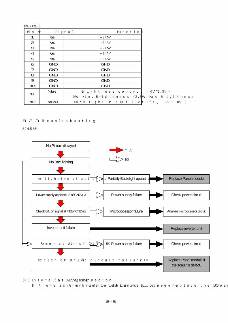
(CN2/CN3)
Pin No Signal Function
1 VINV +24V
2 VINV +24V
3 VINV +24V
4 VINV +24V
5 VINV +24V
6 GND GND
7 GND GND
8 GND GND
9 GND GND
10 GND GND
11 VBR Brightness control ( 0V~3.3V )
0V: Min. Brightness /3.3V: Max Brightness
12 VOnOff Back Light On / Off ( 0V : Off, 5V : On )
8-2-3 Troubleshooting
37WL56P
(※) Ensure the wiring fitting at the connector.
If there is the brightened line or none brightened line regardless the picture, replace the LCD panel module.
No Bacl lighting
No lighting at all or partially no lighting
Power supply at pins#1-5 of CN2 & 3
Check B/L on signal at #12of CN2 &3
No Picture diplayed
Inverter unit failure
Scaler or drive circuit failure(※)
Partially Back light opens
Power supply failure
Micropocessor failure
Replace inverter unit
Replace Panel module if the scaler is defect.
Replace Panel module
Check power circuit
Analyze micrpocessor circuit
YES
NO
Power at #1-4 of CN1 is OK Power supply failure Check power circuit
8-9
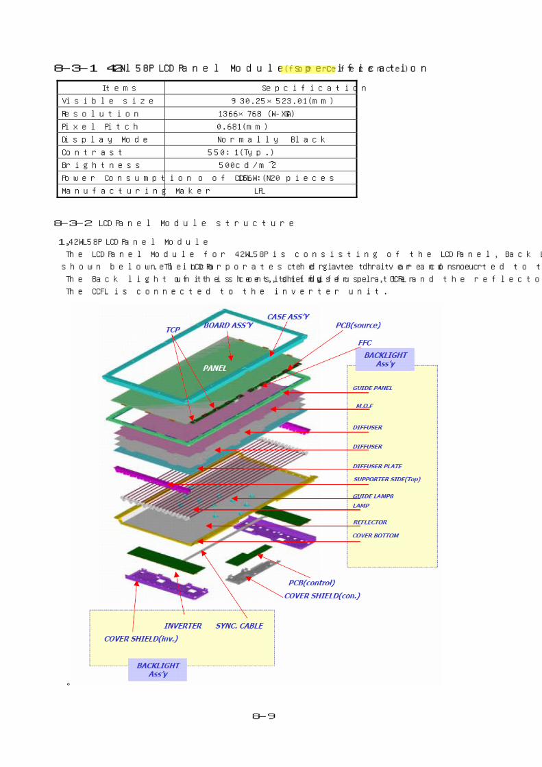
8-3-1 42Wl58P LCD Panel Module specification (for reference)
Items Sepcification
Visible size 930.25×523.01(mm)
Resolution 1366×768 (W-XGA)
Pixel Pitch 0.681(mm)
Display Mode Normally Black
Contrast 550:1(Typ.)
Brightness 500cd/m^2
Power Consumption 166W (No of CCFL : 20 pieces
Manufacturing Maker LPL
8-3-2 LCD Panel Module structure
1,42WL58P LCD Panel Module
The LCD Panel Module for 42WL58P is consisting of the LCD Panel, Back Light unit, the inverter unit and the drive unit as
shown below. The LCD Panel incorporates the gate driver and source drive that are connected to the drive unit through FPC.
The Back light unit is consisting of the sheet, diffuser platter, the diffuser, CCFL and the reflector.
The CCFL is connected to the inverter unit.
。
8-10
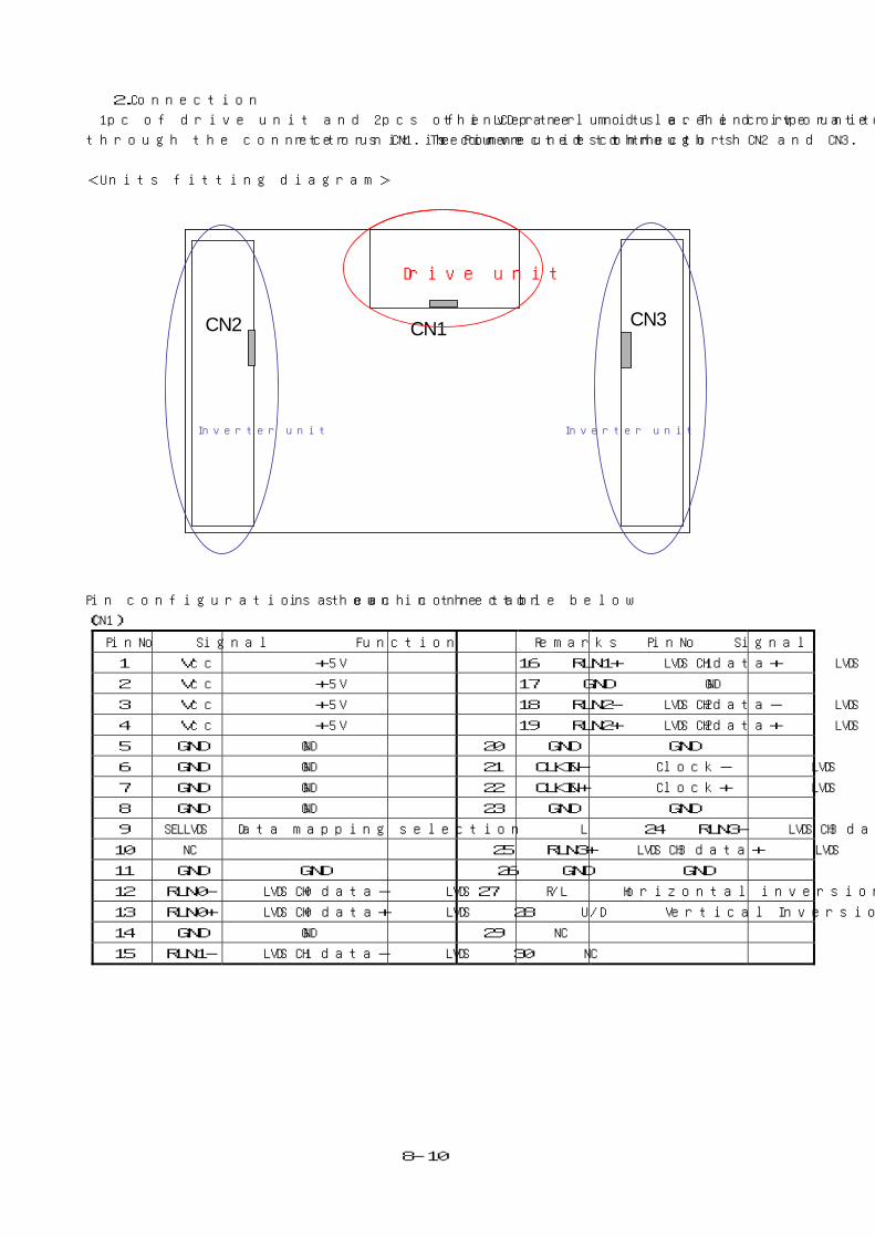
2.Connection
1pc of drive unit and 2pcs of inverter units are incorporated in the LCD panel module. The drive unit is connected to Signal unit
through the connectors CN1. The inverter unit is connected to the Power units through the connectors CN2 and CN3.
<Units fitting diagram>
Pin configuration at each connector is shown in the table below
(CN1)
PinNo Signal Function Remarks PinNo Signal Function Remarks
1 Vcc +5V 16 RLN1+ LVDS CH1data+ LVDS
2 Vcc +5V 17 GND GND
3 Vcc +5V 18 RLN2- LVDS CH2data- LVDS
4 Vcc +5V 19 RLN2+ LVDS CH2data+ LVDS
5 GND GND 20 GND GND
6 GND GND 21 CLKIN- Clock- LVDS
7 GND GND 22 CLKIN+ Clock+ LVDS
8 GND GND 23 GND GND
9 SELLVDS Data mapping selection L 24 RLN3- LVDS CH3 data- LVDS
10 NC 25 RLN3+ LVDS CH3 data+ LVDS
11 GND GND 26 GND GND
12 RLN0- LVDS CH0 data- LVDS 27 R/L Horizontal inversion
13 RLN0+ LVDS CH0 data+ LVDS 28 U/D Vertical Inversion
14 GND GND 29 NC
15 RLN1- LVDS CH1 data- LVDS 30 NC
CN1
ドライブ基板
CN3
インバータ基板マスタ側
インバータ基板 スレーブ側
CN2
CN1
Drive unit
CN3
Inverter unit Inverter unit
CN2
8-11
(CN2/CN3)
Pin No Signal Function
1 VINV +24V
2 VINV +24V
3 VINV +24V
4 VINV +24V
5 VINV +24V
6 GND GND
7 GND GND
8 GND GND
9 GND GND
10 GND GND
11 VBR Brightness control ( 0V~3.3V )
0V: Min. Brightness /3.3V: Max Brightness
12 VOnOff Back Light On / Off ( 0V : Off, 5V : On )
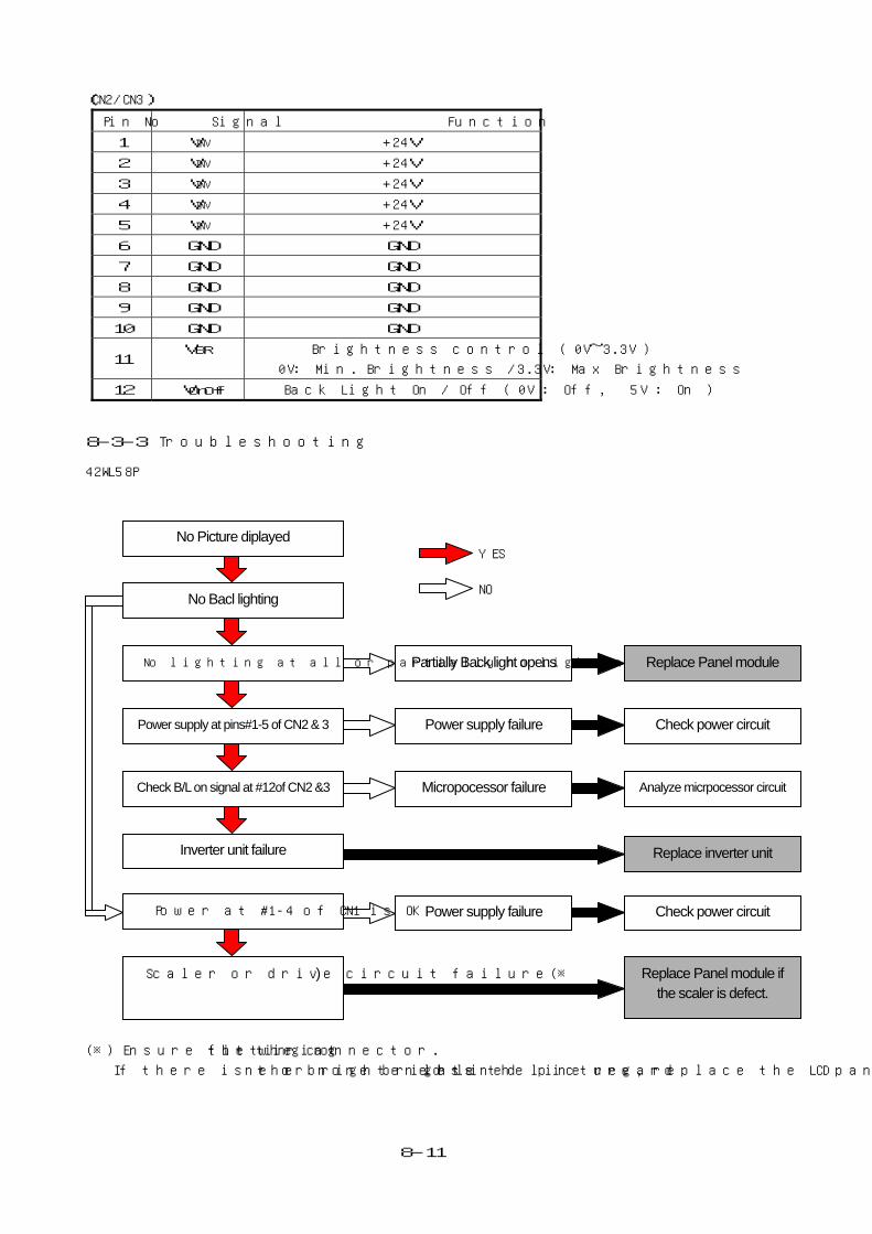
8-3-3 Troubleshooting
42WL58P
(※) Ensure the wiring fitting at the connector.
If there is the brightened line or none brightened line regardless the picture, replace the LCD panel module.
No Bacl lighting
No lighting at all or partially no lighting
Power supply at pins#1-5 of CN2 & 3
Check B/L on signal at #12of CN2 &3
No Picture diplayed
Inverter unit failure
Scaler or drive circuit failure(※)
Partially Back light opens
Power supply failure
Micropocessor failure
Replace inverter unit
Replace Panel module if the scaler is defect.
Replace Panel module
Check power circuit
Analyze micrpocessor circuit
YES
NO
Power at #1-4 of CN1 is OK Power supply failure Check power circuit
8-12
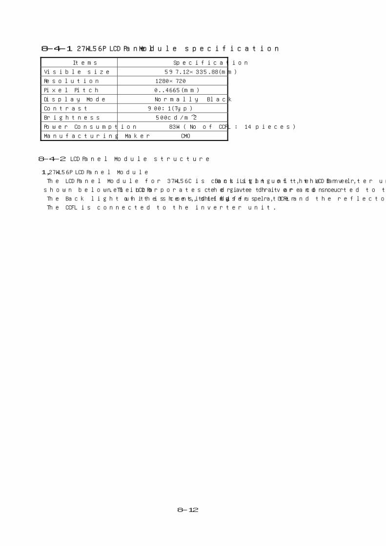
8-4-1 27WL56P LCD Panel Module specification
Items Specification
Visible size 597.12×335.88(mm)
Resolution 1280×720
Pixel Pitch 0..4665(mm)
Display Mode Normally Black
Contrast 900:1(Typ)
Brightness 500cd/m^2
Power Consumption 83W ( No of CCFL : 14 pieces)
Manufacturing Maker CMO
8-4-2 LCD Panel Module structure
1,27WL56P LCD Panel Module
The LCD Panel Module for 37WL56C is consisting of the LCD Panel, Back Light unit, the inverter unit and the drive unit as
shown below. The LCD Panel incorporates the gate driver and source drive that are connected to the drive unit through FPC.
The Back light unit is consisting of the sheet, diffuser platter, the diffuser, CCFL and the reflector.
The CCFL is connected to the inverter unit.
8-13
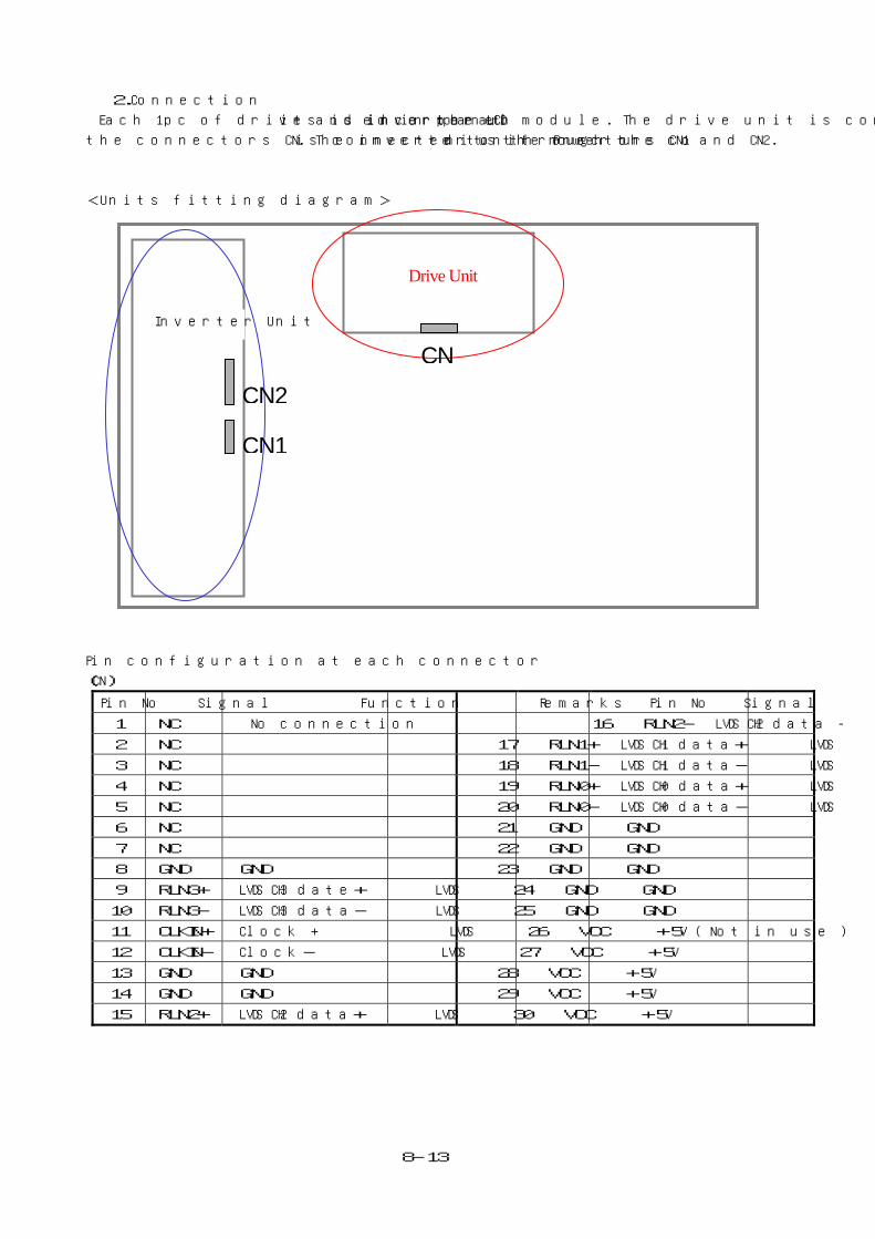
2.Connection
Each 1pc of drive and inverter units is incorporated in the LCD panel module. The drive unit is connected to Signal unit through
the connectors CN. The inverter unit is connected to the Power units through the connectors CN1 and CN2.
<Units fitting diagram>
Pin configuration at each connector
(CN)
Pin No Signal Function Remarks Pin No Signal Function Remarks
1 NC No connection 16 RLN2- LVDS CH2 data - LVDS
2 NC 17 RLN1+ LVDS CH1 data+ LVDS
3 NC 18 RLN1- LVDS CH1 data- LVDS
4 NC 19 RLN0+ LVDS CH0 data+ LVDS
5 NC 20 RLN0- LVDS CH0 data- LVDS
6 NC 21 GND GND
7 NC 22 GND GND
8 GND GND 23 GND GND
9 RLN3+ LVDS CH3 date+ LVDS 24 GND GND
10 RLN3- LVDS CH3 data- LVDS 25 GND GND
11 CLKIN+ Clock + LVDS 26 VCC +5V ( Not in use )
12 CLKIN- Clock- LVDS 27 VCC +5V
13 GND GND 28 VCC +5V
14 GND GND 29 VCC +5V
15 RLN2+ LVDS CH2 data+ LVDS 30 VCC +5V
Drive Unit
CNCN2
CN1
Inverter Unit
8-14
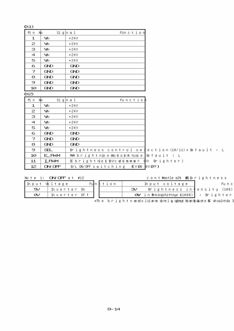
(CN1)
Pin No Signal FUnction
1 VINV +24V
2 VINV +24V
3 VINV +24V
4 VINV +24V
5 VINV +24V
6 GND GND
7 GND GND
8 GND GND
9 GND GND
10 GND GND
(CN2)
Pin No Signal Function
1 VINV +24V
2 VINV +24V
3 VINV +24V
4 VINV +24V
5 VINV +24V
6 GND GND
7 GND GND
8 GND GND
9 SEL Brightness control selection(10/11): Default : L
10 E_PWM PWM brightness control ‐ Not in use Default : L
11 I_PWM DC brightness control ( 3V: dimmer 0V: Brighter)
12 ON/OFF B/L ON/OFF switching (5V:ON 0V:OFF)
Note 1: ON/OFF at #12 Note 2: DC brightness control at #11
Input Voltage Function Input voltage Function
5V Inverter On 3V Brightness intensity (10%) : Dimmer
0V Inverter Off 0V Brightness intensity (100%) : Brighter
*The brightness can be controlled linearly by input DC voltage between 0 and 3V.

8-15
8-4-3 Troubleshooting
27WL56P
(※) Ensure the wiring fitting at the connector.
If there is the brightened line or none brightened line regardless the picture, replace the LCD panel module.
No Bacl lighting
No lighting at all or partially no lighting
Power supply at pins#1-5 of CN2 & 3
Check B/L on signal at #12of CN2
No Picture diplayed
Inverter unit failure
Scaler or drive circuit failure(※)
Partially Back light opens
Power supply failure
Micropocessor failure
Replace inverter unit
Replace Panel module if the scaler is defect.
Replace Panel module
Check power circuit
Analyze micrpocessor circuit
YES
NO
Power at #27-30 of CN is OK Power supply failure Check power circuit

- 9-1 -
Test signal selection : a button (on Remote)Selection of the adjustment items : Channel s/t (on TV or Remote)Change of the data value : Volume ; +/– (on TV or Remote)Adjustment menu mode ON/OFF : MENU button (on TV)Initialization of the memory : CALL + Channel button on TV (s)Reset the count of operating protect
circuit to “00”: CALL + Channel button on TV (t)“RCUT” selection : 1 button“GCUT” selection : 2 button“BCUT” selection : 3 button“SCNT” selection : 4 button“COLP” selection : 5 button“TNTC” selection : 6 button
Color thickness correctionnote: Displayed differently as shown below, de-
pending on the setting of the receiving colorsystem.COLP (PAL)COLC (NTSC)COLS (SECAM)
Automatic A/D Adjustment(PC, Component) : 7 buttonSelf diagnostic display ON/OFF : 9 button
CAUTION : Never try to perform initialization unless you have changed the memory IC.
Capture 9 SERVICE MODE
9-1. ENTERING SERVICE MODE
1) Press button once on 2) Press button again and 3) While pressing the button,
Remote Control. keep pressing. press MENU button on TV set.
(Service mode display)
9-2. DISPLAYING THE ADJUSTMENT MENU
1) Press MENU button on TV.
Service mode Adjustment mode
9-3. KEY FUNCTION IN THE SERVICE MODE
The following key entry during display of adjustment menu provides special functions.
Press
Press
or Sound Mute
- 9-2 -
9-4. SELECTING THE ADJUSTING ITEMS1) Every pressing of CHANNEL s button in the service mode changes the adjustment items in the order of table-2.
(t button for reverse order)
9-5. ADJUSTING THE DATA1) Pressing of VOLUME ; +/– button will change the value of data in the range from 00H to FFH. The variable range
depends on the adjusting item.
9-6. EXIT FROM SERVICE MODE1) Pressing POWER button to turn off the TV once.
■ INITIALIZATION OF MEMORY DATAAfter replacing EEPROM IC, the following initialization is required.
1. Enter the service mode, then select any register item.2. Press and hold the CALL button on the Remote, then press the CHANNEL s button on the TV.The initialization of EEPROM IC
has been complated.3. Check the picture carefully. If necessary, adjust any adjustment item above.
Perform “Auto tune” on the owner’s manual. CAUTION: Never attempt to initialize the data unless EEPROM IC has been replaced.
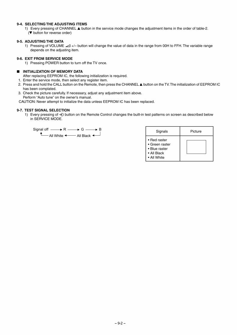
9-7. TEST SIGNAL SELECTION1) Every pressing of a button on the Remote Control changes the built-in test patterns on screen as described below
in SERVICE MODE.
Signals Picture
• Red raster• Green raster• Blue raster• All Black• All White
R
All BlackAll White
BSignal off G
- 9-3 -
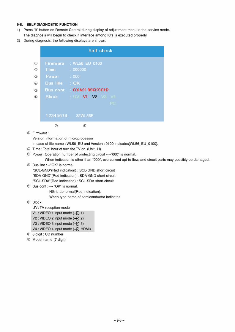
9-8. SELF DIAGNOSTIC FUNCTION
1) Press “9” button on Remote Control during display of adjustment menu in the service mode.
The diagnosis will begin to check if interface among IC’s is executed properly.
2) During diagnosis, the following displays are shown.
1 Firmware :
Version information of microprocessor
In case of file name : WL56_EU and Version : 0100 indicates[WL56_EU_0100].
2 Time : Total hour of turn the TV on. (Unit : H)
3 Power :Operation number of protecting circuit ----"000" is normal.
When indication is other than "000", overcurrent apt to flow, and circuit parts may possibly be damaged.
4 Bus line : --"OK" is normal
"SCL-GND"(Red indication) : SCL-GND short circuit
"SDA-GND"(Red indication) : SDA-GND short circuit
"SCL-SDA"(Red indication) : SCL-SDA short circuit
5 Bus cont : --- "OK" is normal.
NG is abnormal(Red indication).
When type name of semiconductor indicates.
6 Block
UV : TV reception mode
V1 : VIDEO 1 input mode ( 1)
V2 : VIDEO 2 input mode ( 2)
V3 : VIDEO 3 input mode ( 3)
V4 : VIDEO 4 input mode ( HDMI)
7 8 digit : CD number
8 Model name (7 digit)
000
000000
32WL56P32WL56P
WL56_EU_0100WL56_EU_01001
2
3
4
5
6
7 8
- 9-4 -
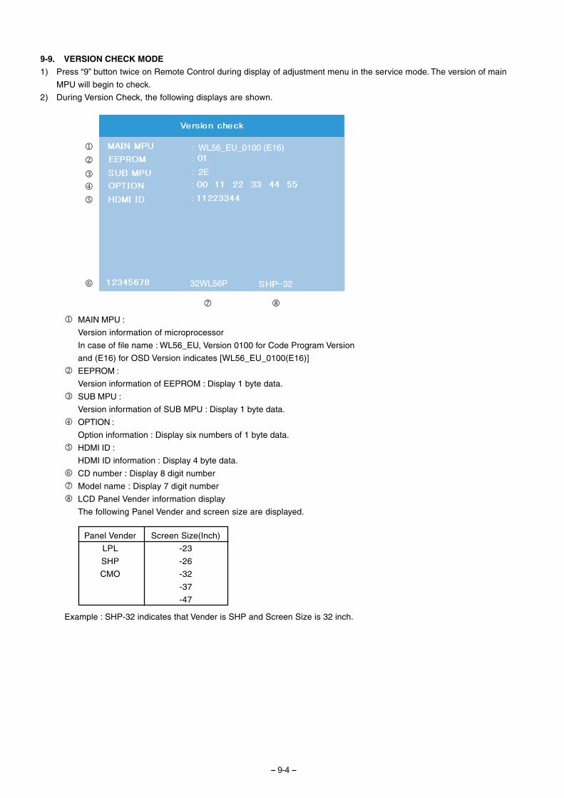
9-9. VERSION CHECK MODE
1) Press “9” button twice on Remote Control during display of adjustment menu in the service mode. The version of main
MPU will begin to check.
2) During Version Check, the following displays are shown.
1 MAIN MPU :
Version information of microprocessor
In case of file name : WL56_EU, Version 0100 for Code Program Version
and (E16) for OSD Version indicates [WL56_EU_0100(E16)]
2 EEPROM :
Version information of EEPROM : Display 1 byte data.
3 SUB MPU :
Version information of SUB MPU : Display 1 byte data.
4 OPTION :
Option information : Display six numbers of 1 byte data.
5 HDMI ID :
HDMI ID information : Display 4 byte data.
6 CD number : Display 8 digit number
7 Model name : Display 7 digit number
8 LCD Panel Vender information display
The following Panel Vender and screen size are displayed.
WL56_EU_0100 (E16)
2E
32WL56P 32
1
2
34
5
6
7 8
Panel Vender Screen Size(Inch)
LPL -23
SHP -26
CMO -32
-37
-47
Example : SHP-32 indicates that Vender is SHP and Screen Size is 32 inch.
- 9-5 -
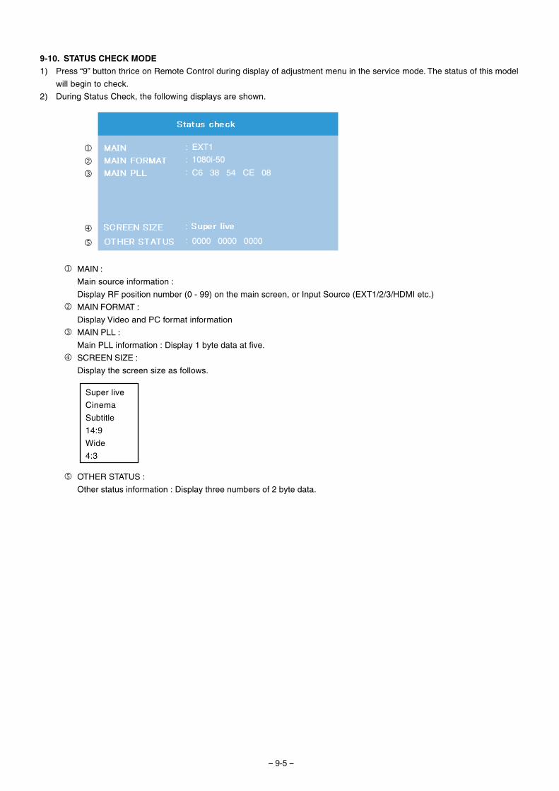
9-10. STATUS CHECK MODE
1) Press “9” button thrice on Remote Control during display of adjustment menu in the service mode. The status of this model
will begin to check.
2) During Status Check, the following displays are shown.
1 MAIN :
Main source information :
Display RF position number (0 - 99) on the main screen, or Input Source (EXT1/2/3/HDMI etc.)
2 MAIN FORMAT :
Display Video and PC format information
3 MAIN PLL :
Main PLL information : Display 1 byte data at five.
4 SCREEN SIZE :
Display the screen size as follows.
5 OTHER STATUS :
Other status information : Display three numbers of 2 byte data.
Super live
Cinema
Subtitle
14:9
Wide
4:3
EXT1
1080i-50
C6 38 54 CE 08
0000 0000 0000
1
2
4
5
3

FILE NO. 336-9707
TECHNICAL TRAINING MANUAL
3 LCD DATA PROJECTOR
PRINTED IN JAPAN, Nov., 1997 S
TLP511UTLP510UTLP511ETLP510E
���������������� 1-1, SHIBAURA 1-CHOME, MINATO-KU, TOKYO 105-01, JAPAN