lecture 13: alu & sequential logic - uc santa barbara
TRANSCRIPT
Lecture 13: !ALU & Sequential Logic !
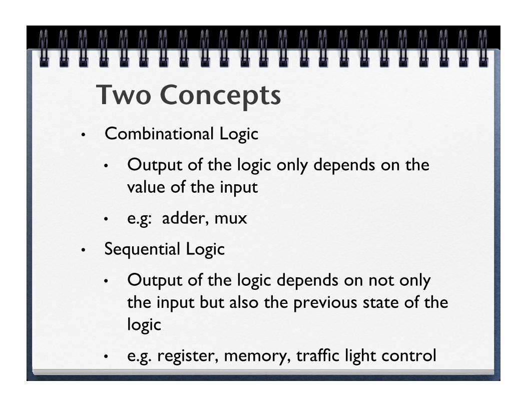
Two Concepts!• Combinational Logic
• Output of the logic only depends on the value of the input
• e.g: adder, mux
• Sequential Logic
• Output of the logic depends on not only the input but also the previous state of the logic
• e.g. register, memory, traffic light control

An Abstract View of the CPU!
Data Out
Clk
5
Rw Ra Rb 32 32-bit Registers
Rd
ALU
Clk
Data In
Data Address Ideal
Data Memory
Instruction
Instruction Address
Ideal Instruction
Memory
Clk
PC
5 Rs
5 Rt
32
32 32 32 A
B
Nex
t Add
ress
Control
Datapath
Control Signals Conditions
MUX & ALU!
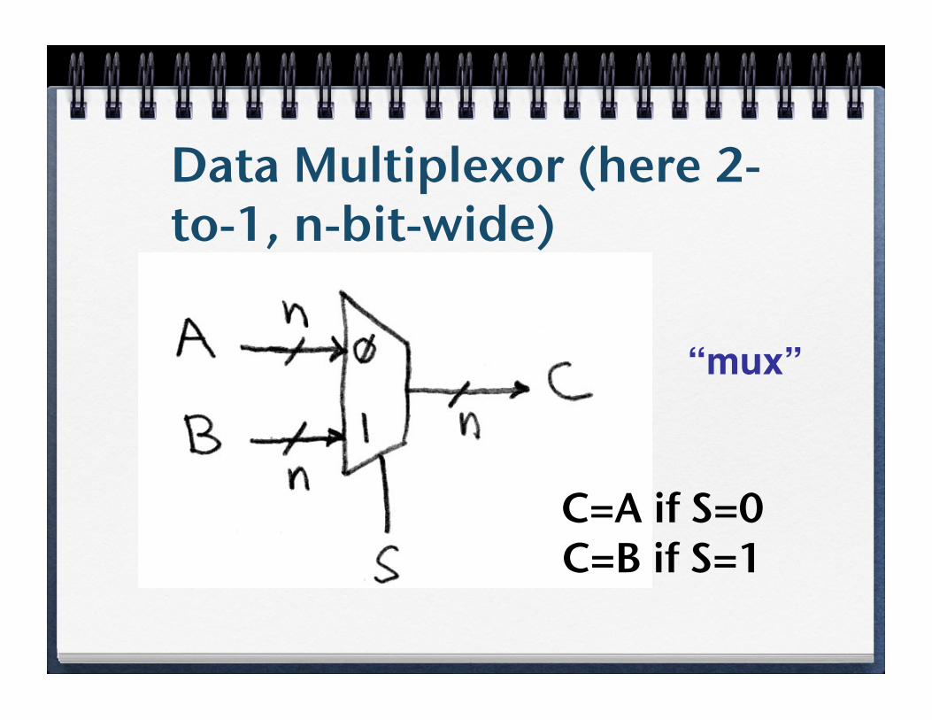
Data Multiplexor (here 2-to-1, n-bit-wide)!
“mux”!
C=A if S=0!C=B if S=1!
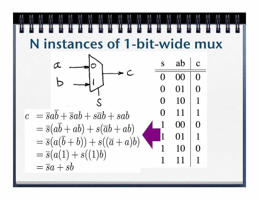
N instances of 1-bit-wide mux!
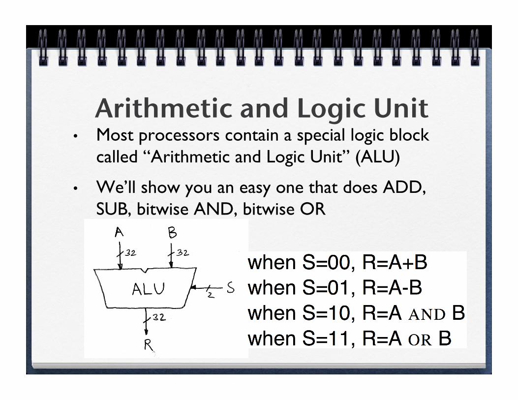
Arithmetic and Logic Unit!• Most processors contain a special logic block
called “Arithmetic and Logic Unit” (ALU)
• We’ll show you an easy one that does ADD, SUB, bitwise AND, bitwise OR
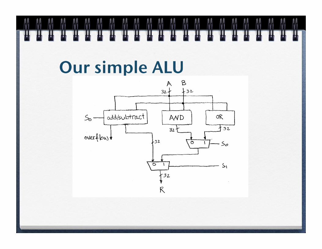
Our simple ALU!

Arithmetic Logic Units (1)!
A 1-bit ALU.
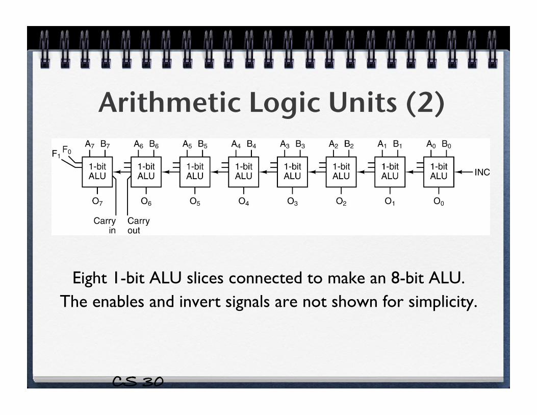
Arithmetic Logic Units (2)!
Eight 1-bit ALU slices connected to make an 8-bit ALU. The enables and invert signals are not shown for simplicity.
CS 30 !
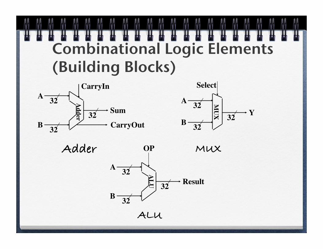
Combinational Logic Elements !(Building Blocks)!
32
32
A
B 32 Sum
CarryOut
Adder
CarryIn
Adder!
32 A
B 32
Y 32
Select
MU
X
MUX!
32
32
A
B 32 Result
OP
ALU
ALU!
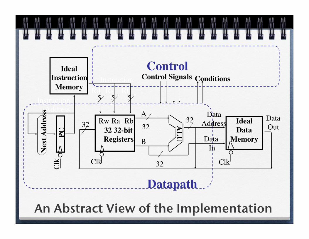
An Abstract View of the Implementation!
Data Out
Clk
5
Rw Ra Rb 32 32-bit Registers
Rd
ALU
Clk
Data In
Data Address Ideal
Data Memory
Instruction
Instruction Address
Ideal Instruction
Memory
Clk
PC
5 Rs
5 Rt
32
32 32 32 A
B
Nex
t Add
ress
Control
Datapath
Control Signals Conditions
Sequential logic!Memory
element: latches,
flip-flops!
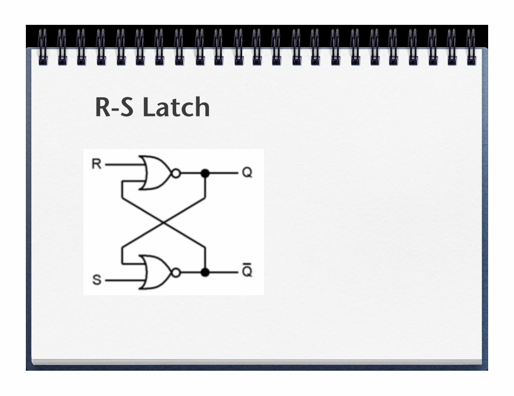
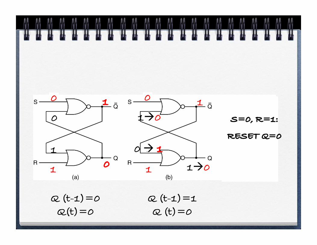
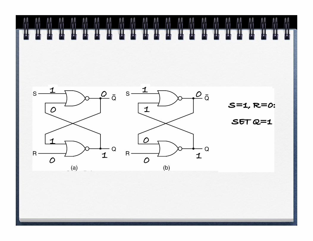
R-S Latch!
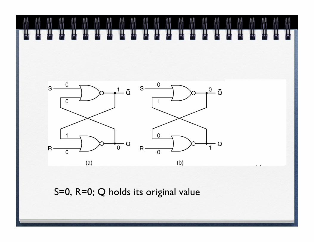
S=0, R=0; Q holds its original value
0!
0!
1!
1!
1! 0!
0!
0 1!
10!
1!
1!
10!
S=0, R=1:!
RESET Q=0!
Q (t-1)=0!Q(t)=0!
Q (t-1)=1!Q (t)=0!
CS 30 !
1!
0!
0!
1!
0! 1!
1!
0!
1!
0! 1!
0!S=1, R=0:!
SET Q=1!
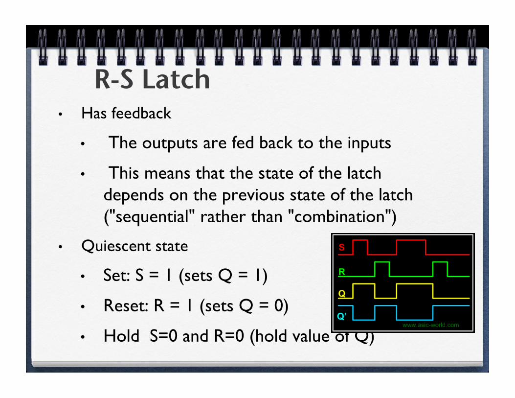
R-S Latch!• Has feedback
• The outputs are fed back to the inputs
• This means that the state of the latch depends on the previous state of the latch ("sequential" rather than "combination")
• Quiescent state
• Set: S = 1 (sets Q = 1)
• Reset: R = 1 (sets Q = 0)
• Hold S=0 and R=0 (hold value of Q)
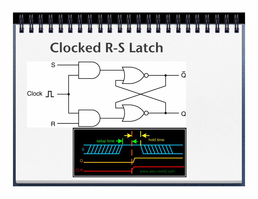
Clocked R-S Latch!

Clocked D Latches !D CK Q
0 1 0
1 1 1
X 0 Q0
Truth table!
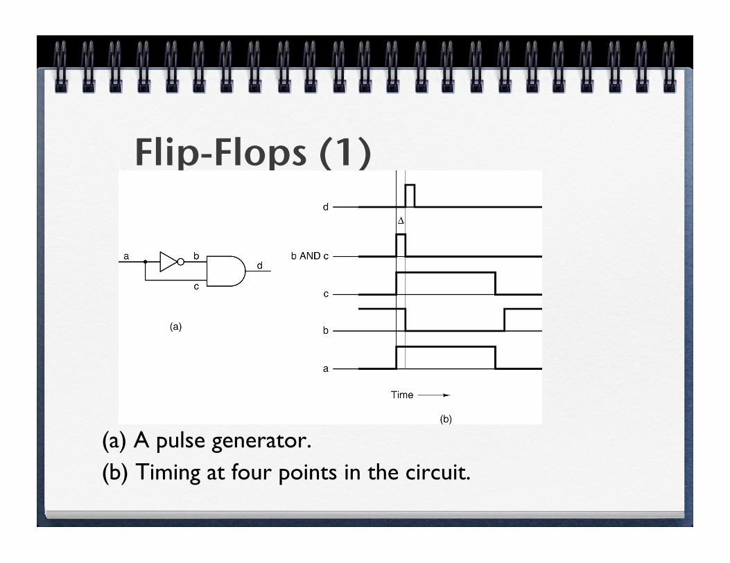
Flip-Flops (1)!
(a) A pulse generator. (b) Timing at four points in the circuit.

Flip-Flops (2) – D flip flop!
CS 30 !
D CK Q
0 ↑ 0
1 ↑ 1
X 0,1 Q0
Truth table!
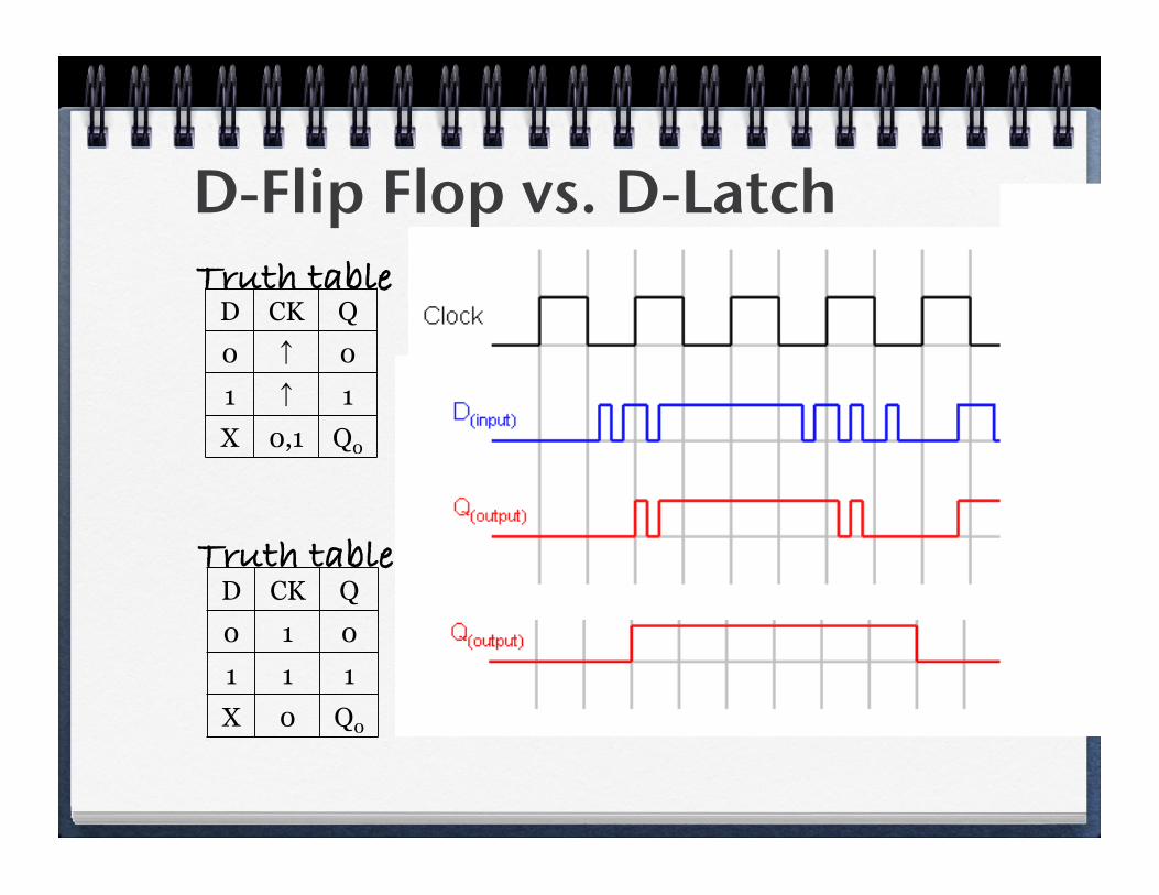
D-Flip Flop vs. D-Latch!
D CK Q
0 1 0
1 1 1
X 0 Q0
Truth table!
D CK Q
0 ↑ 0
1 ↑ 1
X 0,1 Q0
Truth table!

An Abstract View of the Implementation!
Data Out
Clk
5
Rw Ra Rb 32 32-bit Registers
Rd
ALU
Clk
Data In
Data Address Ideal
Data Memory
Instruction
Instruction Address
Ideal Instruction
Memory
Clk
PC
5 Rs
5 Rt
32
32 32 32 A
B
Nex
t Add
ress
Control
Datapath
Control Signals Conditions
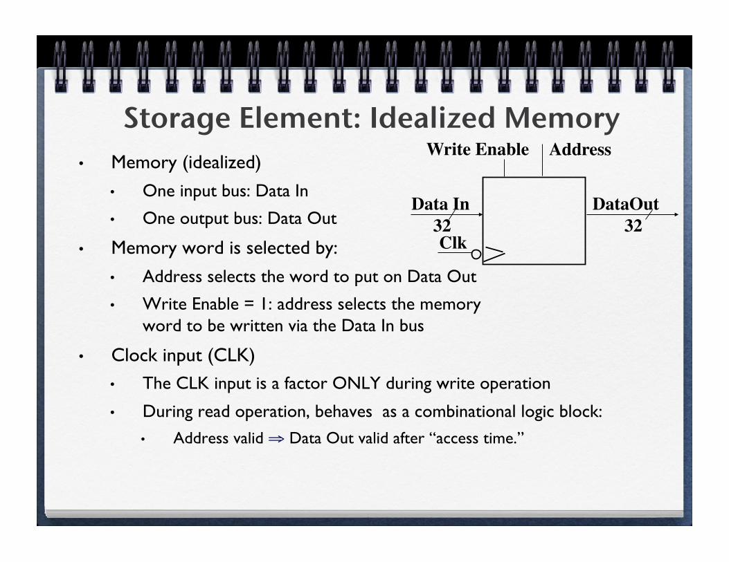
Storage Element: Idealized Memory!• Memory (idealized)
• One input bus: Data In
• One output bus: Data Out
• Memory word is selected by:
• Address selects the word to put on Data Out
• Write Enable = 1: address selects the memory���word to be written via the Data In bus
• Clock input (CLK) • The CLK input is a factor ONLY during write operation
• During read operation, behaves as a combinational logic block:
• Address valid ⇒ Data Out valid after “access time.”
Clk
Data In
Write Enable
32 32 DataOut
Address
Clk
Data In
Write Enable
N N Data Out
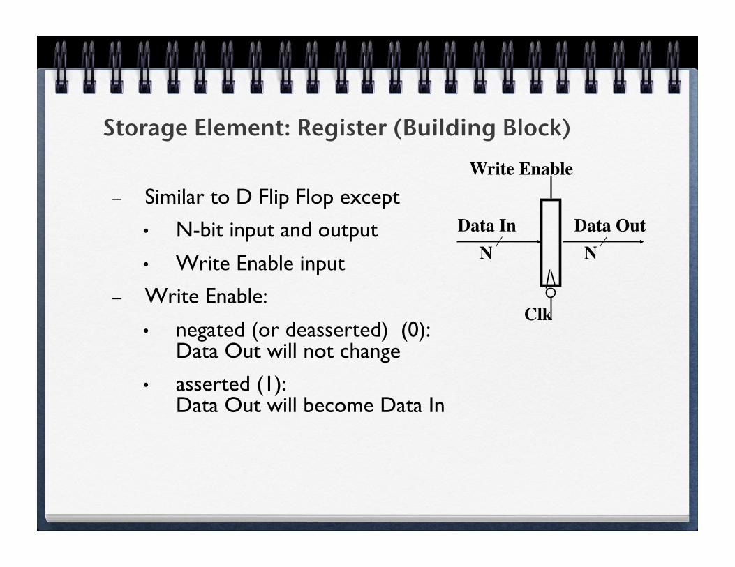
Storage Element: Register (Building Block)!
– Similar to D Flip Flop except
• N-bit input and output
• Write Enable input
– Write Enable:
• negated (or deasserted) (0): ���Data Out will not change
• asserted (1): ���Data Out will become Data In
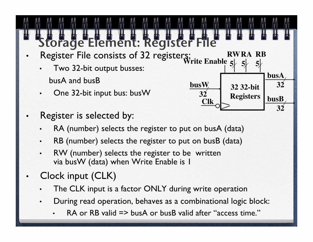
Storage Element: Register File!• Register File consists of 32 registers:
• Two 32-bit output busses:
busA and busB
• One 32-bit input bus: busW���
• Register is selected by: • RA (number) selects the register to put on busA (data)
• RB (number) selects the register to put on busB (data) • RW (number) selects the register to be written���
via busW (data) when Write Enable is 1
• Clock input (CLK) • The CLK input is a factor ONLY during write operation
• During read operation, behaves as a combinational logic block: • RA or RB valid => busA or busB valid after “access time.”
Clk
busW
Write Enable
32 32
busA
32 busB
5 5 5 RW RA RB
32 32-bit Registers
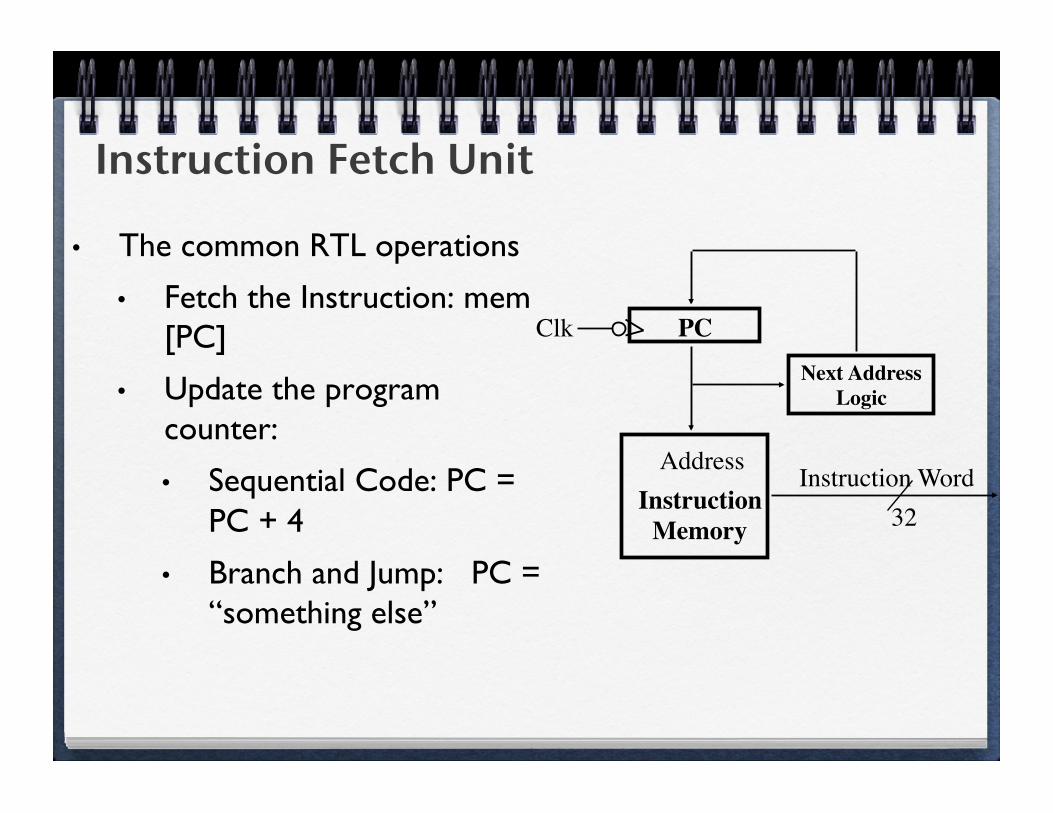
Instruction Fetch Unit!
• The common RTL operations
• Fetch the Instruction: mem[PC]
• Update the program counter:
• Sequential Code: PC = PC + 4
• Branch and Jump: PC = “something else”
32 Instruction Word Address
Instruction Memory
PC Clk Next Address
Logic