lecture 9 - system-on-chips (soc) labesc.inu.ac.kr/~chung/epc6055_2017/lecture_09.pdf · ·...
TRANSCRIPT

Jaeyong Chung
Robust Systems Laboratory
Incheon National University
Digital Integrated Circuits
Lecture 9

DIGITAL DESIGN FLOW
Chung EPC6055 2
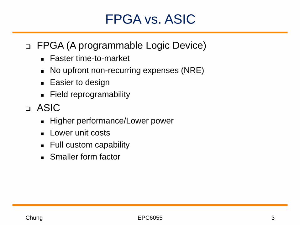
FPGA vs. ASIC
FPGA (A programmable Logic Device)
Faster time-to-market
No upfront non-recurring expenses (NRE)
Easier to design
Field reprogramability
ASIC
Higher performance/Lower power
Lower unit costs
Full custom capability
Smaller form factor
Chung EPC6055 3

FPGA vs. ASIC
Chung EPC6055 4

FPGA vs. CPU+Software
ASIC is chips customized for specific tasks
CPU is general-purpose chips that run software
FPGA is generic chips that can be programmed
FPGA
Good for parallelizable tasks
Provides true concurrency
CPU + Software
Provide high performance for a serial task
Emulates concurrency
Chung EPC6055 5

PROGRAMMABLE LOGIC DEVICES
Chapter 3 – Programmable Logic Devices
Many Ways to Implement Combinational Circuit
NAND, NOR
Multiplexers
Decoders
ROMs (LUTs)
Programmable Logic Device
Puts Different Building Blocks in Chip
Provides Mechanism to Reconfigure (Program) It
Chung EPC6055 6

PROGRAMMABLE LOGIC DEVICES
Chung EPC6055 7

POPULAR PROGRAMMABLE DEVICES
SPLD CPLD FPGA
Density Low
Few hundred gates
Low to Medium
500 to 12,000 gates
Medium to High
3,000 to 5,000,000 gates
Timing Predictable Predictable Unpredictable
Cost Low Low to Medium Medium to High
Major
Vendors
Lattice Semiconductor
Cypress
AMD
Xilinx
Altera
Xilinx
Altera
Actel
Example
Devices
Lattice Semiconductor
GAL16LV8
GAL22V10
Cypress
PALCE16V8
Xilinx
CoolRunner
XC9500
Altera
MAX
Xilinx
Virtex
Spartan
Altera
Stratix
Actel
Accelerator
Chung EPC6055 8

8-WORD x 4-BIT ROM
Chung EPC6055 9

ROM WITH N-INPUT AND M-OUTPUTS
Chung EPC6055 10

BASIC ROM STRUCTURE
Chung EPC6055 11

8-WORD BY 4-BIT ROM
Chung EPC6055 12

EQUIVALENT OR-GATE FOR F0
Chung EPC6055 13

TYPES OF ROMS
ROM – Read Only Memory
PROM – User Programmable ROM
EPROM – Erasable PROM
EEPROM – Electrically Erasable PROM
Flash – Particular Type of EEPROM
Uses Special Type of Charge Storage
Usually Has Built-In Programming and Erasure Capability
Doesn’t Require Separate Programmer Hardware
Chung EPC6055 14

PROGRAMMABLE LOGIC ARRAY
F0 = ∑m(0, 1, 4, 6) = A'B' + AC'
F1 = ∑m(2, 3, 4, 6, 7) = B + AC'
F2 = ∑m(0, 1, 2, 6) = A'B' + BC'
F3 = ∑m(2, 3, 5, 6, 7) = AC + B
Chung EPC6055 15

PROGRAMMABLE ARRAY LOGIC (PAL)
Programmable Array Logic (PAL)
OR Connections Fixed
Cannot Share Products
Less Flexible Than PLA
Example
PAL for I1I'2 + I'1I2
Chung EPC6055 16

GALs
Erasible/Reprogrammable PALs Called
GALs (Generic Array Logic)
EPROM AND EEPROM type
Require Hardware Programmer
Flash type
In-Circuit Programmable
Often PALs Have GAL Equivalents
E.g., PALCE22V10 Equivalent to GAL22V10
Most Also Have Macroblocks
Contain MUXes and Additional Programmability
Chung EPC6055 17

COMPLEX PLDs
Complex PLDs (CPLDs)
Equivalent to Several PLDs on Same Chip
Uses Programmable Interconnect Matrix
Built From Crossbar Switch
NxM Crossbar Switch
Allows N Input Lines to be Connected to Any M Output Lines
Expensive to Build
Provides Predictable Interconnect Delay
Chung EPC6055 18

FPGAs
Field-Programmable Gate Arrays (FPGAs)
ICs Containing Array of Logic Blocks with Programmable
Interconnections
Larger than PALs, PLAs, CPLDs
Invented around 1985
Xilinx XC2000
Xilinx chips - SRAM programmable
In-Circuit Reconfigurable
Chung EPC6055 19

FPGAs vs. MPGAs
Mask Programmable Gate Arrays (MPGAs)
Needs Custom Mask
Programmable Only in Factory
Larger Turn Around Time (Time to Market)
Low Flexibility (Error Necessitates New Mask)
Field Programmable Gate Arrays (FPGAs)
Standard Off the Shelf Products
Needs No Custom Mask
User Can Reprogram Many Times
Negligible Turn Around Time (Fast Time to Market)
High Flexibility (Easy to Change Design and Fix Errors)
Cheaper Than MPGAs at Low Volumes
Chung EPC6055 20

DISADVANTAGES OF FPGAs
Less Dense than MPGAs
Extra Hardware Need to Support Field Programmability
Slower than MPGAs
Programmable Interconnect Results in Higher Resistance
and Capacitance (Longer RC Delay)
Unpredictable Delays
More Power
Chung EPC6055 21

POPULAR XILINX FPGAs
Spartan/XL - 5K to 40K
Spartan 3 - 50K to 5M
Spartan-3E - 100K to 1.6M
Spartan-3L - 1M to 4M
Spartan-II - 15K to 200K
Spartan-IIE - 50K to 600K
Virtex - 57,906 to 1,124,022
Virtex-4 FX - 12,312 to 142,128 LCBs
Virtex-4 LX - 13,824 to 200,448 LCBs
Virtex-4 SX - 23,040 to 55,296 LCBs
Virtex-E - 71,693 to 4,074,387
Virtex-E Extended Memory - 129,600 to 254,016
Virtex-II - 40K to 8M
Virtex-II Pro - 3,168 to 99,216 LCBs
Virtex-II Pro/X - 22,032 to 74,448 LCBs
Chung EPC6055 22

POPULAR ALTERA FPGAs
ACEX 1K - 56K to 257K
APEX 20K - 113K to 2.5M
APEX II - 1.9M to 5.25M
Cyclone - 2,910 to 20,060 LEs
Cyclone II - 4,608 to 68,416 LEs
FLEX 10K - 10K to 50K
FLEX 6000 - 5K - 24K
Mercury - 120K to 350K
Stratix - 10,570 to 79,040 LEs
Stratix GX - 10,570 to 41,250 LEs
Stratix II -15,600 to 179,400 LEs
Stratix II GX - 33,880 to 132,540 LEs
Chung EPC6055 23

POPULAR ACTEL FPGAs
Axcelerator - 125K To 2M
eX - 3K to 12K
SX/SXA - 8K to 72K
ProASIC3 - 30K to 3M
ProASICplus - 75K to 1M
ProASIC - 100 to 450K
MX - 3K to 54K
Chung EPC6055 24
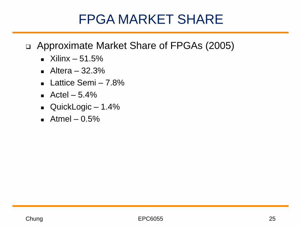
FPGA MARKET SHARE
Approximate Market Share of FPGAs (2005)
Xilinx – 51.5%
Altera – 32.3%
Lattice Semi – 7.8%
Actel – 5.4%
QuickLogic – 1.4%
Atmel – 0.5%
Chung EPC6055 25

FOUR ARCHITECTURES FOR FPGAs
Chung EPC6055 26

TYPICAL MATRIX BASED FPGA LAYOUT
Chung EPC6055 27

SIMPLE CONFIGURABLE LOGIC BLOCK
Chung EPC6055 28

MUX-BASED LOGIC BLOCK
A B C F
0 0 0 0} C
0 0 1 1
0 1 0 1} C '
0 1 1 0
1 0 0 0} 0
1 0 1 0
1 1 0 1} 1
1 1 1 1
Chung EPC6055 29

XILINX VIRTEX CLB
Chung EPC6055 30

GENERAL ROUTING MATRIX
Chung EPC6055 31

SWITCH MATRIX
Chung EPC6055 32

DIRECT INTERCONNECTS
Chung EPC6055 33

GLOBAL LINES
Chung EPC6055 34

PROGRAMMABLE I/O BLOCK
Chung EPC6055 35

EMBEDDED RAM
Distributed RAM from LUTs
Create RAM from LUTs;
Done in Early FPGAs up to XC4000
Had No Dedicated Memory
BlockRAM
Starting with VIRTEX
Blocks of Dedicated Memory Embedded in FPGAs
Variable Width RAM
Chung EPC6055 36

VARIABLE WIDTH RAM ASPECT RATIOS
Width Depth Addr Bus Data Bus
1 32 K 15 bits 1 bit
2 16 K 14 bits 2 bits
4 8 K 13 bits 4 bits
8 4 K 12 bits 8 bits
16 2K 11 bits 16 bits
Chung EPC6055 37

Special
Components
Xilinx
Virtex-4 FX,
Virtex-II Pro
Xilinx
Spartan-3E,
3/3L
Altera
Stratix II
Altera
APEX,
APEX II
DSP
Support
18 X 18
Multipliers
18 X 18
Multipliers
DSP Blocks
Embedded
Multipliers
Embedded
Processor
IBM
PowerPC
400MHz
MicroBlaze,
PicoBlaze
Nios2 ARM,
MIPS,
Nios
Comm.
Support
Multi-
GigaBit
Transceivers
None
Memory Block RAM
Content
Addressable
Mem. (CAM)
No No No Yes
COMPARE FPGAs
Chung EPC6055 38

Spartan-3 FPGA attributes
Chung EPC6055 39
Spartan-3 FPGA Family Data Sheet

Spartan-3 Family Architecture
Chung EPC6055 40
Spartan-3 FPGA Family Data Sheet
Input/Output BlockDigital Clock Manager

CLB of Spartan-3
All four slices have following elements in common: two logic function generators,
two storage elements, wide-function multiplexers, carry logic, and arithmetic and
ROM functions
Besides these, the left-hand pair supports two additional functions: storing data
using Distributed RAM and shifting data with 16-bit registers.
Chung EPC6055 41
Spartan-3 FPGA Family Data Sheet

Slice of Spartan-3
Chung EPC6055 42
Spartan-3 FPGA Family Data Sheet

Design Report of ICE
Chung EPC6055 43

Placement of ICE
Chung EPC6055 44

Chung EPC6055 45
Routing of ICE

APPLICATIONS OF FPGAs
Rapid Prototyping
5 Million Gate FPGAs Allows Large Applications
Can Also Have Multiple FPGAs on Boards
Final Product in Medium Speed Systems
Can Operate in 150-200 MHz Range
Reconfigurable Circuits and Systems
Reconfigurable “Soft” Hardware Systems
Glue Logic
Handle Interface Between Chips
Can Be Updated for Changes in Protocol
Hardware Accelerators/Coprocessors
Implement Key Kernels to Speed Up Application
Chung EPC6055 46

DESIGN FLOW FOR FPGAs
Create Model of Design in HDL
Simulate and Debug Design
Synthesize Design Targeting Desired Device
Run Mapping/Partitioning Program
Maps to CLBs
Run Place and Route Program
Places CLBs and Routes Interconnect
Run Program to Generate Configuration Bits
Download Configuration Bits into FPGA
Chung EPC6055 47

INITIALIZING SRAM-BASED FPGA
Chung EPC6055 48