licatio ote 13 october 2013 wireless power user...
TRANSCRIPT
Application Note 138
AN138-1
an138fc
October 2013
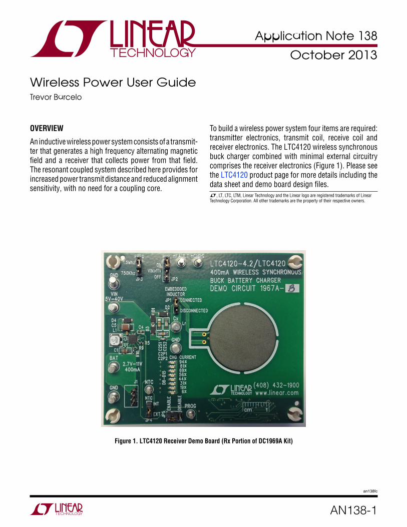
Figure 1. LTC4120 Receiver Demo Board (Rx Portion of DC1969A Kit)
OVERVIEW
An inductive wireless power system consists of a transmit-ter that generates a high frequency alternating magnetic field and a receiver that collects power from that field. The resonant coupled system described here provides for increased power transmit distance and reduced alignment sensitivity, with no need for a coupling core.
Wireless Power User GuideTrevor Barcelo
L, LT, LTC, LTM, Linear Technology and the Linear logo are registered trademarks of Linear Technology Corporation. All other trademarks are the property of their respective owners.
To build a wireless power system four items are required: transmitter electronics, transmit coil, receive coil and receiver electronics. The LTC4120 wireless synchronous buck charger combined with minimal external circuitry comprises the receiver electronics (Figure 1). Please see the LTC4120 product page for more details including the data sheet and demo board design files.

Application Note 138
AN138-2
an138fc
Figure 3. Proxi-Point Transmitter Figure 4. Proxi-2D Transmitter
Figure 2. Implementation of Basic Transmitter Reference Design (Tx Portion of DC1969A Kit)
Application Note 138
AN138-3
an138fc
Transmitter Solutions
Currently there are four transmitter options available for design or off-the-shelf purchase:
1. Basic: This wireless power design (Figure 2) was developed by collaboration between PowerbyProxi Inc. and Linear Technology. It is provided as an open source reference design that can be used to integrate the LTC4120 into a wireless power system. The details of the push-pull current-fed resonant converter are described later in this document.
2. Proxi-Point: This is an advanced transmitter (Figure 3) that is available from PowerbyProxi. For further infor-mation visit www.powerbyproxi.com. It is ready to use or incorporate directly into a product. Unlike the basic transmitter, it offers features such as foreign metal detec-tion, low standby power and a stable crystal-controlled operating frequency. The transmit coil is built in.
3. Proxi-2D: This is an advanced transmitter (Figure 4) that is available from PowerbyProxi. For further informa-tion visit www.powerbyproxi.com. It is ready to use or incorporate directly into a product. Unlike Proxi-Point, it is capable of charging multiple receivers simultane-ously in any orientation on the 2D charging surface. The transmit coil is built in.
4. Proxi Custom: If the above options are not suitable for your application, a custom transmitter can be designed and manufactured to meet your requirements. Please con-tact PowerbyProxi at [email protected] for further information and pricing or visit www.powerbyproxi.com.
BASIC TRANSMITTER
The basic transmitter for the LTC4120, described in the following sections, combined with a receive coil and LTC4120-based receiver electronics can be used to produce a wireless battery charging system. This wire-less battery charging system enables evaluation of the LTC4120 using standard components.
Basic is a resonant DC-AC transmitter. It is a simple, easy and inexpensive transmitter designed to work with the LTC4120. Pre-regulation is required to provide a relatively precise DC input voltage to meet a given set of receive power requirements. The basic transmitter does not feature foreign object metal detection and can therefore cause these objects to heat up. Furthermore, the operating fre-quency of the basic transmitter can vary with component selection and load.
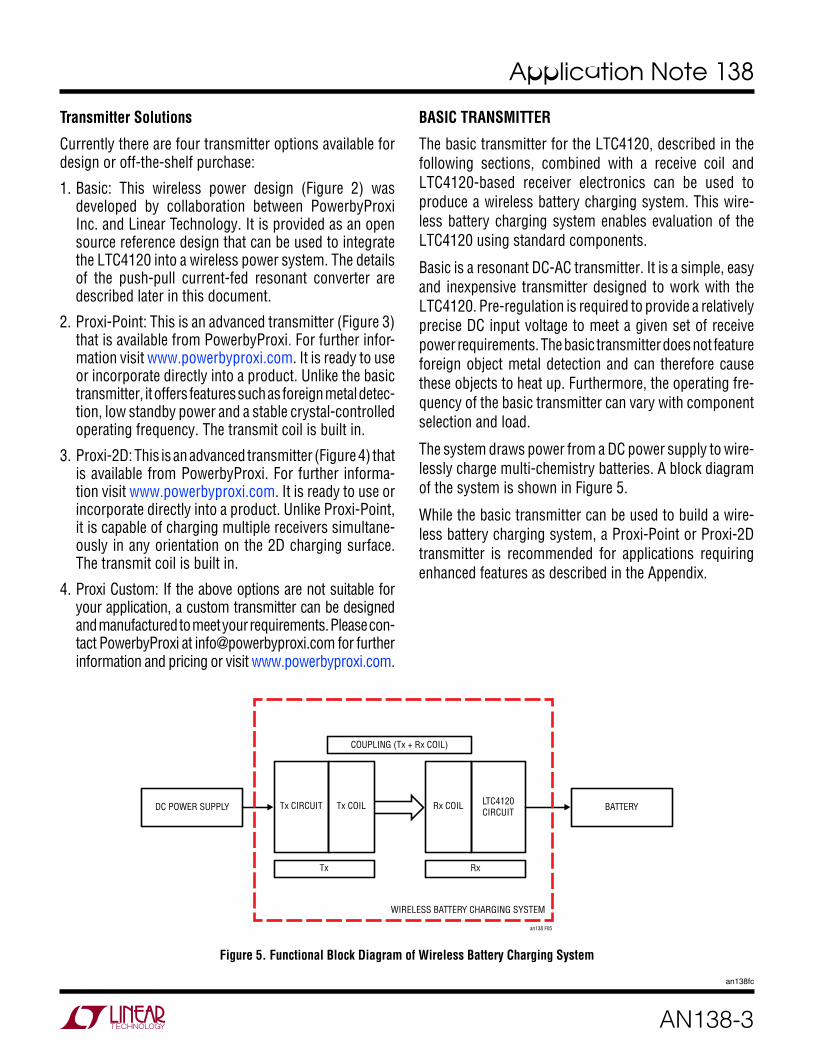
The system draws power from a DC power supply to wire-lessly charge multi-chemistry batteries. A block diagram of the system is shown in Figure 5.
While the basic transmitter can be used to build a wire-less battery charging system, a Proxi-Point or Proxi-2D transmitter is recommended for applications requiring enhanced features as described in the Appendix.
Figure 5. Functional Block Diagram of Wireless Battery Charging System
DC POWER SUPPLY
WIRELESS BATTERY CHARGING SYSTEM
BATTERY
COUPLING (Tx + Rx COIL)
Tx Rx
Tx CIRCUIT LTC4120CIRCUIT
Tx COIL Rx COIL
an138 F05

Application Note 138
AN138-4
an138fc
System Functional Block Description
LTC4120-based wireless battery charging systems use wireless power transfer technology with Dynamic Harmo-nization Control (DHC), a patented technique that enables optimal wireless power transfer across a variety of condi-tions while providing thermal management and overvoltage protection. The resonant coupled system described here eliminates both the need for precise mechanical alignment as well as the need for a coupling core. The charging system is composed of transmitter electronics, transmit coil, receive coil and receiver electronics.
The transmit coil, LX, is energized by the transmitter electronics to generate a high frequency magnetic field (typically around 130kHz, though the operating frequency varies depending on the load at the receiver and the cou-pling to the receive coil). This magnetic field induces a voltage in the power receive coil, LR. After being tuned with a capacitor, this induced voltage is managed by the LTC4120 in order to control the power transfer. A typical transmitter generates an AC coil current of about 2.5A RMS.
The receive coil, LR, is configured in a resonant circuit followed by a rectifier and the LTC4120. Please see the LTC4120 product page for more details including the data sheet and demo board design files. The receive coil presents a load reflected back to the transmitter through the mutual inductance between LR and LX. The reflected impedance of
the receiver may influence the operating frequency of the transmitter. Likewise, the power output by the transmitter depends on the load at the receiver. The charging system, consisting of both the transmitter and LTC4120 charger, provides an efficient method for wireless battery charging. The power output by the transmitter varies automatically based on the power used to charge a battery.
Circuit Description
The basic transmitter is a current-fed push-pull transmit-ter capable of delivering 2W to the battery output of the LTC4120. The basic transmitter schematic is shown in Figure 6. The switches in this push-pull transmitter are driven from the voltage on the opposing leg and no ad-ditional control circuitry is required to drive them. The switch driving circuitry consists of a resistor, turn-off diode, gate capacitor and a Zener diode for each switch.
The voltage rating of the Zener diodes D1 and D4 is cho-sen to fully turn on M1 and M2 while protecting them from overvoltage.
The current limiting gate resistors R1 and R2 are selected according to the maximum VDS of M1, M2 and the current rating of the Zener diodes.
The resultant voltage waveforms across LX are shown in
C40.01µF
R1100Ω
C50.01µF
CX0.3µF
LX5µH
68µH
LB1• •68µH
LB2
VDC5V TRANSMITTER
R2100Ω
D3
M1 M2
D2
D1BZX84C16
D4BZX84C16
an138 F06
Figure 6. Schematic of a Basic Transmitter for LTC4120
Application Note 138
AN138-5
an138fc
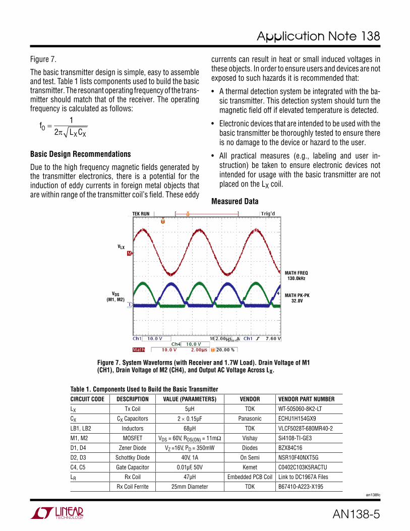
Figure 7.
The basic transmitter design is simple, easy to assemble and test. Table 1 lists components used to build the basic transmitter. The resonant operating frequency of the trans-mitter should match that of the receiver. The operating frequency is calculated as follows:
fO =
12π LX CX
Basic Design Recommendations
Due to the high frequency magnetic fields generated by the transmitter electronics, there is a potential for the induction of eddy currents in foreign metal objects that are within range of the transmitter coil’s field. These eddy
currents can result in heat or small induced voltages in these objects. In order to ensure users and devices are not exposed to such hazards it is recommended that:
• A thermal detection system be integrated with the ba-sic transmitter. This detection system should turn the magnetic field off if elevated temperature is detected.
• Electronic devices that are intended to be used with the basic transmitter be thoroughly tested to ensure there is no damage to the device or hazard to the user.
• All practical measures (e.g., labeling and user in-struction) be taken to ensure electronic devices not intended for usage with the basic transmitter are not placed on the LX coil.
Measured Data
Table 1. Components Used to Build the Basic TransmitterCIRCUIT CODE DESCRIPTION VALUE (PARAMETERS) VENDOR VENDOR PART NUMBER
LX Tx Coil 5µH TDK WT-505060-8K2-LT
CX CX Capacitors 2 × 0.15µF Panasonic ECHU1H154GX9
LB1, LB2 Inductors 68µH TDK VLCF5028T-680MR40-2
M1, M2 MOSFET VDS = 60V, RDS(ON) = 11mΩ Vishay Si4108-TI-GE3
D1, D4 Zener Diode VZ =16V, PD = 350mW Diodes BZX84C16
D2, D3 Schottky Diode 40V, 1A On Semi NSR10F40NXT5G
C4, C5 Gate Capacitor 0.01µF, 50V Kemet C0402C103K5RACTU
LR Rx Coil 47µH Embedded PCB Coil Link to DC1967A Files
Rx Coil Ferrite 25mm Diameter TDK B67410-A223-X195
Figure 7. System Waveforms (with Receiver and 1.7W Load). Drain Voltage of M1 (CH1), Drain Voltage of M2 (CH4), and Output AC Voltage Across LX.
TEK RUN
VDS(M1, M2)
VLX
an138 F07
MATH FREQ130.0kHz
MATH PK-PK32.8V
Application Note 138
AN138-6
an138fc
Table 2.Basic Transmitter Circuit Parameters (4.5mm Gap)
SPECIFICATION
WITHOUT RECEIVER (STANDBY)
WITH RECEIVER (NO LOAD)
WITH RECEIVER
(1.58W LOAD)
Operational Frequency 130.5kHz 128.7kHz 128.9kHz
Input Voltage 4.99V 4.99V 4.95V
Input Current 0.15A 0.173A 0.676A
RMS Value of Tx Output AC Voltage
10.9V 10.8V 10.4V
Peak Value of Tx Output AC Voltage
15.2V 15.2V 15.2V
Receiver Output DC Voltage
N/A 34.9V 27V
Standby Loss 0.75W 0.873W N/A
Efficiency N/A N/A 47.1%
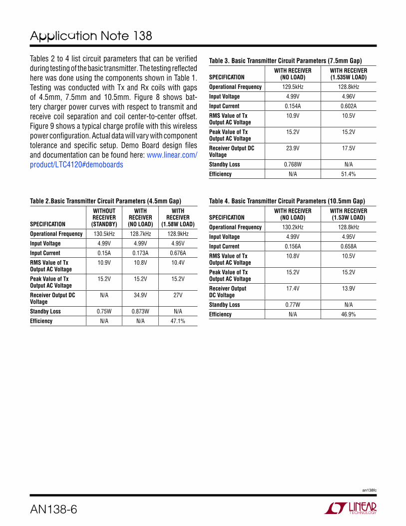
Table 3. Basic Transmitter Circuit Parameters (7.5mm Gap)
SPECIFICATIONWITH RECEIVER
(NO LOAD)WITH RECEIVER (1.535W LOAD)
Operational Frequency 129.5kHz 128.8kHz
Input Voltage 4.99V 4.96V
Input Current 0.154A 0.602A
RMS Value of Tx Output AC Voltage
10.9V 10.5V
Peak Value of Tx Output AC Voltage
15.2V 15.2V
Receiver Output DC Voltage
23.9V 17.5V
Standby Loss 0.768W N/A
Efficiency N/A 51.4%
Table 4. Basic Transmitter Circuit Parameters (10.5mm Gap)
SPECIFICATIONWITH RECEIVER
(NO LOAD)WITH RECEIVER (1.53W LOAD)
Operational Frequency 130.2kHz 128.8kHz
Input Voltage 4.99V 4.95V
Input Current 0.156A 0.658A
RMS Value of Tx Output AC Voltage
10.8V 10.5V
Peak Value of Tx Output AC Voltage
15.2V 15.2V
Receiver Output DC Voltage
17.4V 13.9V
Standby Loss 0.77W N/A
Efficiency N/A 46.9%
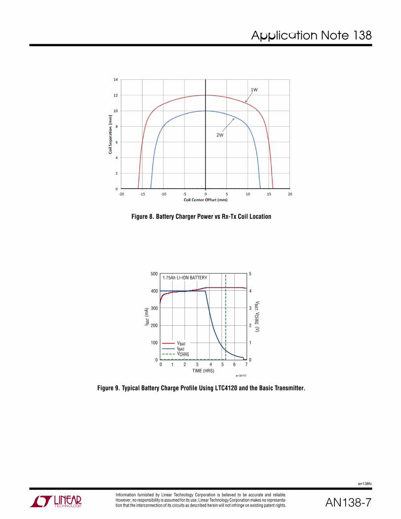
Tables 2 to 4 list circuit parameters that can be verified during testing of the basic transmitter. The testing reflected here was done using the components shown in Table 1. Testing was conducted with Tx and Rx coils with gaps of 4.5mm, 7.5mm and 10.5mm. Figure 8 shows bat-tery charger power curves with respect to transmit and receive coil separation and coil center-to-center offset. Figure 9 shows a typical charge profile with this wireless power configuration. Actual data will vary with component tolerance and specific setup. Demo Board design files and documentation can be found here: www.linear.com/product/LTC4120#demoboards
Application Note 138
AN138-7
an138fc
Information furnished by Linear Technology Corporation is believed to be accurate and reliable. However, no responsibility is assumed for its use. Linear Technology Corporation makes no representa-tion that the interconnection of its circuits as described herein will not infringe on existing patent rights.
Figure 9. Typical Battery Charge Profile Using LTC4120 and the Basic Transmitter.
TIME (HRS)0
0
100
I BAT
(mA)
200
300
400
500
0
VBAT , V
CHRG (V)
2
1
3
4
5
1 2 3 4 5 6 7
an138 F07
VCHRGIBAT
VBAT
1.75Ah LI-ION BATTERY
Figure 8. Battery Charger Power vs Rx-Tx Coil Location

Application Note 138
AN138-8
an138fc
Linear Technology Corporation1630 McCarthy Blvd., Milpitas, CA 95035-7417 (408) 432-1900 ● FAX: (408) 434-0507 ● www.linear.com LINEAR TECHNOLOGY CORPORATION 2013
LT 1214 REV C • PRINTED IN USA
APPENDIX: PROXI-POINT AND PROXI-2D
The patented Proxi-Point and Proxi-2D transmitters are available as fully assembled, tested and certified off-the-shelf solutions from PowerbyProxi. For further information visit, www.powerbyproxi.com.
The receive coil is configured in a resonant circuit followed by a rectifier and the LTC4120. The transmitter frequency is controlled by a crystal oscillator and will not vary significantly from the designed value. The power output by the transmitter depends on the load at the receiver. The impedance of the resonant receiver presents a load reflected back to the transmitter, so the transmitted power will automatically vary depending on receiver power as the LTC4120 charges the battery. The wireless power charging system—consisting of either the Proxi-Point or Proxi-2D transmitter and the LTC4120-based receiver—provides an efficient method for wireless battery charging.
Table 5. Features and Functions of Transmitter OptionsFEATURES AND FUNCTIONS BASIC PROXI-POINT PROXI-2D
Rated Power 2W 2W 2W per Receiver
Receivers per Transmitter Single Single Multiple
Freedom of Placement × × √
Intelligent Foreign Metal Object Detection*
× √ √
EMC/EMI Compliant Off-The-Shelf × √ √
Fixed Operating Frequency × √ √
Supplied AC/DC Adaptor × √ √
Reverse-Polarity Protection × √ √
Built-In Transmit Coil × √ √
Low Power Standby** × √ √
Available for Purchase × √ √
*This feature is a way of preventing foreign metal objects from heating when they are placed over the transmit coil.
**This feature allows the transmitter to autonomously enter a low power state when there is no receiver within charging range of a transmitter or if the receiver in range does not require power.
Table 5 compares features offered by the various trans-mitter options.
Further details regarding Proxi-Point, Proxi-2D and Proxi custom solutions can be found at www.powerbyproxi.com