linear integrated circuits€¦ · difference between digital ic and linear ic ... 741, 741a, 741c,...
TRANSCRIPT
0
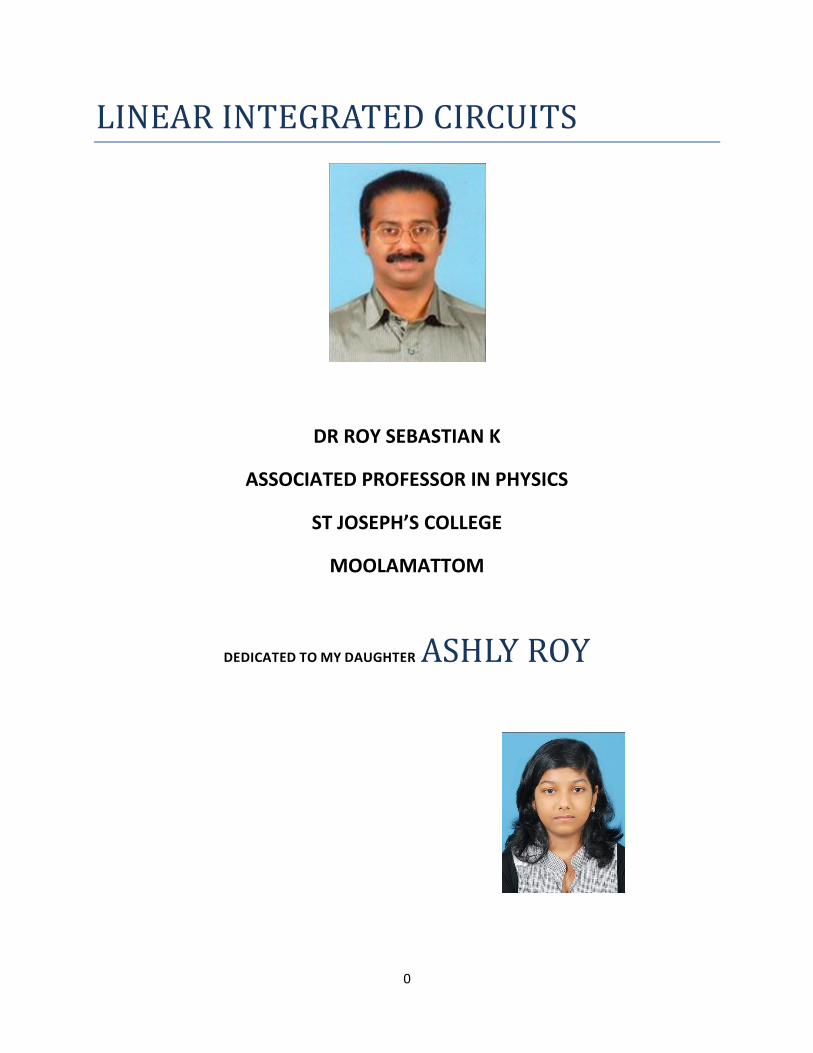
LINEAR INTEGRATED CIRCUITS
DR ROY SEBASTIAN K
ASSOCIATED PROFESSOR IN PHYSICS
ST JOSEPH’S COLLEGE
MOOLAMATTOM
DEDICATED TO MY DAUGHTER ASHLY ROY

1
CHAPTER 1
THE OPERATIONAL AMPLIFIER (OP AMP)
An operational amplifier is a direct-coupled high gain amplifier usually consisting of one or more
differential amplifiers followed by a level translator (shifter) and an output stage. The output stage is
generally a push-pull or push-pull complementary symmetry pair. An op-amp is available as a single
integrated circuit package.
The op-amp can be used to amplify both A.C. and D.C. signals. Op-amp can be used for
performing mathematical operations such as addition, subtraction, multiplication, integration and
differentiation etc. and thus get the name operational amplifier.
Block diagram representation of a typical op-am
Since an op-amp is a multistage amplifier, it can be represented by a block diagram as shown in
figure.
The first stage is the dual input, balanced output differential amplifier. This stage generally
provides most of the voltage gain of the amplifier and also establishes the input resistance of the op-
amp. The second stage is usually another differential amplifier, which is driven by the output of the first
stage. In most amplifiers the second stage is dual input, unbalanced output (single ended). Because
direct coupling is used in these stages, the dc voltage at the output of the second stage is well above
ground potential. Therefore, generally the level translator (shifting) circuit is used after the
intermediate stage to shift the dc level at the output of the intermediate stage downward to zero volts
with respect to ground. The final stage is usually a push- pull complementary amplifier output stage.
The output stage increases the output voltage swing and raises the current supplying capability of the
op-amp. A well designed output stage also provides low output resistance.

2
Schematic symbol
Figure shows the schematic symbol for the op-amp.
For simplicity power supply and other pin connections are omitted. Since the inputs differential
amplifier stage of the op-amp is designed to be operated in the differential mode, the differential inputs
are designed by the (+) and (-) notations. The (+) input is the non-inverting input. An ac signal (or dc
voltage) applied to this input produces an in phase (or same polarity) signal at the output. On the other
hand the (-) input is the inverting input because an ac signal (or dc) applied to this input produces an
180° out of phase (or opposite polarity) signal at the output.
In the schematic symbol
Voltage at the non-inverting input =V1
Voltage at the inverting input = V2
Output voltage = Vo
All these voltages are measured w.r.t. ground
Large signal voltage gain = A
3
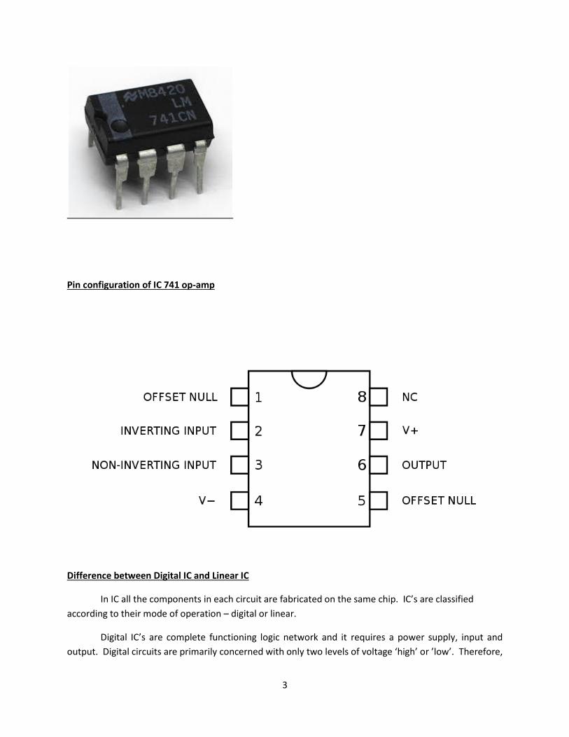
Pin configuration of IC 741 op-amp
Difference between Digital IC and Linear IC
In IC all the components in each circuit are fabricated on the same chip. IC’s are classified
according to their mode of operation – digital or linear.
Digital IC’s are complete functioning logic network and it requires a power supply, input and
output. Digital circuits are primarily concerned with only two levels of voltage ‘high’ or ’low’. Therefore,
4
accurate control of operating region characteristic is not required in digital circuit, unlike in linear circuit.
For this reason, digital circuits are easy to design and are produced in large quantities as low cost
devices.
Linear IC’s are equivalent of discrete transistor networks, such as amplifiers, filters, frequency
multipliers and modulators that often require additional external components for satisfactory operation.
For example, external resistors are necessary to control the voltage gain and frequency response of an
op-amp. In linear circuits the output electrical signals vary in proportion to the input signals applied or
the physical quantities they represent. Since the electrical signals are analogous to the physical
quantities, linear circuits are also referred to as analog circuits.
Power supplies for Op-amp
Most linear IC’s (particularly op-amp) use one or more differential amplifier stages and
differential amplifiers require both a positive and negative power supply for proper operation of the
circuit. This means that most linear IC’s need both a positive and negative power supply. A few linear
IC’s use unequal power supplies and some IC’s require only a positive supply. For example the 702 op-
amp requires unequal power supplies, whereas the 324 requires only a positive power supply. Some
dual supply op-amp IC’s can also be operated from a single supply voltage provided that a special
external circuit is used with it. The two power supplies required for a linear IC are usually equal in
magnitude, +15V and -15V, for example.
Manufacturer’s designations for integrated circuits
There is large number of IC manufactures producing millions of IC’s per year. Each
manufacturer uses a specific code and assigns a specific type number to the IC’s produced by them.
Each manufacturer uses its own identifying initials followed by its own type number. For example, the
741 type of internally compensated op-amp was originally manufactured by Fairchild and is sold as the
µA741, where ‘µA’ represent the identifying initials used by Fairchild. Initials used by some of the well
known manufactures of linear IC’s are as follows
Fairchild : - µA &µAF
National semiconductor: - LM, LH, LF and TBA
Motorola: - MC & MFC
RCA :- CA & CD
Signetics: - N/S, NE/SE &SU
Texas Instruments: - SN
5
The initials used by manufacturers in designing digital IC’s may differ from those used for linear
IC’s. For example DM and CD are the initials used for digital monolithic and CMOS digital IC’s
respectively by National Semiconductor.
In addition to producing their own IC’s a number of manufacturers also produce one another’s
popular IC’s. In such IC’s the manufactures usually retain the original type number of the IC in their own
IC designation. For example, Fairchild’s original µA741 is also manufactured by various other
manufacturers under their own designations as follows
National semiconductor: - LM 741
Motorola: - MC1 741
RCA: - CA3 741
Texas Instruments: - SN52 741
Signetics: - N5 741
Note that the last three digits in each manufacturer’s designation are 741. All these op-amps have the
same specifications, and therefore, behave the same.
Some linear IC’s are available in different classes, such as A, C, E, S and SE. For example, the
741, 741A, 741C, 741E, 741S and 741SE are different versions of the same op-amp. The 741 is a military
grade op-amp (operating temperature range:- -55°C to +125°C) and the 741C is a commercial grade op-
amp (operating temp. range:- 0°C to +70/75°C). On the other hand 741A and 741E are improved
versions of the 741 and 741C respectively.
Package types
There are three basic types of linear IC packages
(a) The flat pack
(b) The metal can or transistor pack
(c) The dual-in-line package (for short DIP)
If the IC is used for experimentation/bread boarding purpose, the best choice is the DIP
package, because it is easy to mount. The flat pack is more reliable and lighter than a
comparable DIP package and is, therefore, suited for airborne applications. On the other hand,
the metal can is the best choice if the IC is to be operated at relatively high power and expected
to dissipate considerable heat.
Temperature ranges
1. Military temperature range : -55°C to +125°C (or -55°C to +85°C)
2. Industrial temperature range: -20°C to +85°C (or -40°C to +85°C)
3. Commercial temperature range: 0°C to +75°C)

6
Military and commercial grade IC’s differ in specifications for supply voltages, input current and
voltage offsets and drifts, voltage gain, etc. The military grade devices are almost always of superior
quality, and costly. Commercial grade IC’s had the worst tolerance among the three types but is the
cheapest.
Ordering Information
Generally in ordering an IC the following information must be specified: device type, package type
and temperature range. The device type is a group of alphanumeric characters such as µA 741. The
basic package type (flat pack, DIP etc) is represented by one letter. The military, industrial or
commercial temperature range is either numerically specified or included in the device type number
or represented by a letter. For example
Characteristics of an Op-amp
1. Input offset voltage
Input offset voltage is the voltage that must be applied between the two input terminals of an op-
amp to null the output as shown in figure.
Vio = |Vdc1 –Vdc2|
In the figure Vdc1 and Vdc2 are dc voltages and Rs represents the source resistance. We denote
input offset voltage by Vio. This voltage Vio could be positive or negative. For a 741 IC the
maximum value of Vio is 6mV dc. The smaller the value of Vio, the better the input terminals is
matched.
7
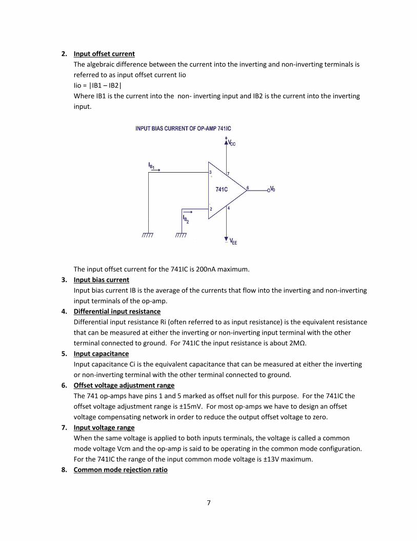
2. Input offset current
The algebraic difference between the current into the inverting and non-inverting terminals is
referred to as input offset current Iio
Iio = |IB1 – IB2|
Where IB1 is the current into the non- inverting input and IB2 is the current into the inverting
input.
The input offset current for the 741IC is 200nA maximum.
3. Input bias current
Input bias current IB is the average of the currents that flow into the inverting and non-inverting
input terminals of the op-amp.
4. Differential input resistance
Differential input resistance Ri (often referred to as input resistance) is the equivalent resistance
that can be measured at either the inverting or non-inverting input terminal with the other
terminal connected to ground. For 741IC the input resistance is about 2MΩ.
5. Input capacitance
Input capacitance Ci is the equivalent capacitance that can be measured at either the inverting
or non-inverting terminal with the other terminal connected to ground.
6. Offset voltage adjustment range
The 741 op-amps have pins 1 and 5 marked as offset null for this purpose. For the 741IC the
offset voltage adjustment range is ±15mV. For most op-amps we have to design an offset
voltage compensating network in order to reduce the output offset voltage to zero.
7. Input voltage range
When the same voltage is applied to both inputs terminals, the voltage is called a common
mode voltage Vcm and the op-amp is said to be operating in the common mode configuration.
For the 741IC the range of the input common mode voltage is ±13V maximum.
8. Common mode rejection ratio

8
Common mode rejection ratio (CMRR) is defined as the ratio of the differential voltage gain (Ad)
to the common mode voltage gain (A cm)
i.e. CMRR = Ad/A cm
The differential voltage gain Ad is the same as the large signal voltage gain A. Common mode
voltage gain, A cm = V0 cm/Vi cm
Where Vo cm = output common mode voltage
Vi cm = input common mode voltage
A cm = common mode voltage gain
Generally the A cm is very small and Ad = A is very large, therefore, the CMRR is very large.
Being a large value, CMRR is most often expressed in decibels (dB).
CMRR in dB = 20 log10 (Ad/A cm)
Problem 1: A differential dc amplifier has a differential mode gain of 100 and a common mode gain
0.01. What is its CMRR in dB?
Solution:
CMRR in dB = 20 log (Ad/A cm) = 20 log (100/0.01) = 20 log (10000) = 20 x 4 =80dB.
Problem 2: For a given op-amp, CMRR = 104 and differential gain Ad = 105. What is the common mode
gain?
Solution:
CMRR = Ad/ A cm
A cm = Ad/CMRR = 105/104 = 10
9. Supply voltage rejection ratio
The change in an op-amp input offset voltage Vio caused by variations in supply voltages is
called the supply voltage rejection ration (SVRR) or power supply rejection ratio (PSRR) or power
supply sensitivity (PSS). For 741IC SVRR = 150 µV/V. Lower the value of SVRR the better for op-
amp performance.
10. Large signal voltage gain
Since the op-amp amplifies difference voltage between two input terminals, the voltage gain of
the amplifier is defined as
Voltage gain = output voltage/differential input voltage
i.e. A = Vo/Vid
Because output signal amplitude is much larger than the input signal, the voltage gain is
commonly called large signal voltage gain. Under test condition the large signal voltage gain of
the 741IC is 2 lacks typically.
11. Output voltage swing

9
The output voltage swing Vo (max) of the 741 IC is guaranteed to be between -13V to +13V for
RL ≥ 2KΩ. i.e. a 26 V peak-to-peak undistorted sine wave for ac input signals. The output voltage
swing indicates the values of positive and negative saturation voltages of the op-amp.
12. Output resistance
Output resistance Ro is the equivalent resistance that can be measured between the output
terminal of the op-amp and the ground. It is 75Ω for the 741 op-amp.
13. Output short circuit current
If the output of the op-amp is shorted to ground, the current will be much higher than IB of Iio.
This high current may damage the op-amp if it does not have output short circuit protection.
However, the 741 family op-amps have built in short circuit protection circuit.
14. Supply current
Supply current Is is the current drawn by the op-amp from the power supply. For the 741IC op-
amp the supply current Is = 2.8mA.
15. Power consumption
Power consumption Pc is the amount of quiescent power (Vin = 0V) that must be consumed by
the op-amp in order to operate properly. The amount of power consumed by the 741C is
85mW.
16. Transient response
The response of any practically useful network to a given input is composed of two parts: the
transient and steady state response. The transient response is that portion of the complete
response before the output attains some fixed value. Once reached, this fixed value remains at
that level and is, therefore, referred to as a steady state value. The response of the network
after it attains a fixed value is independent of time and is called the steady state response.
Unlike the steady state response the transient response is time variant. The rise time and the
presence of overshoot are the characteristics of the transient response. The time required by
the output to go from 10% to 90% of its final value is called the rise time. Conversely
overshoot is the maximum amount by which the output deviates from the steady state value.
Overshoot is generally expressed as a percentage.
The rise time0.3µs and overshoot is 5% for the 741C op-amp.
The transient response is one of the important considerations in selecting an op-amp in ac
applications. In fact, the rise time is inversely proportional to the unity gain bandwidth of the
op-amp. This means that the smaller the value of rise time the higher is the band width.
17. Slew rate
Slew rate (SR) is defined as the maximum rate of change of output voltage per unit time. It is
expressed in volts per microseconds.
i.e. Slew rate = (dVo/dt) maximum V/µs
Slew rate indicates how rapidly the output of an op-amp can change in response to changes in
the input frequency. The slew rate changes with change in voltage gain and is normally
specified at unity gain. The slew rate of an op-amp is fixed, therefore, if the slope requirement
of the output signal are greater than the slew rate, then distortion occurs. Thus slew rate is one
of the important factors in selecting the op-amp for ac applications, particularly at relatively
high frequencies.
10
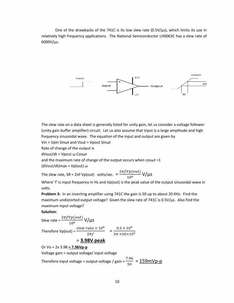
One of the drawbacks of the 741C is its low slew rate (0.5V/µs), which limits its use in
relatively high frequency applications. The National Semiconductor LH0063C has a slew rate of
6000V/µs.
The slew rate on a data sheet is generally listed for unity gain, let us consider a voltage follower
(unity gain buffer amplifier) circuit. Let us also assume that input is a large amplitude and high
frequency sinusoidal wave. The equation of the input and output are given by
Vin = Vpin Sinωt and Vout = Vpout Sinωt
Rate of change of the output is
dVout/dt = Vpout ω Cosωt
and the maximum rate of change of the output occurs when cosωt =1
(dVout/dt)max = Vp(out) ω
The slew rate, SR = 2πf Vp(out) volts/sec. =
V/µs
Where’ f’ is input frequency in Hz and Vp(out) is the peak value of the output sinusoidal wave in
volts.
Problem 3: In an inverting amplifier using 741C the gain is 50 up to about 20 KHz. Find the
maximum undistorted output voltage? Given the slew rate of 741C is 0.5V/µs. Also find the
maximum input voltage?
Solution:
Slew rate =
V/µs
Therefore Vp(out) =
=
= 3.98V peak Or Vo = 2x 3.98 = 7.96Vp-p
Voltage gain = output voltage/ input voltage
Therefore input voltage = output voltage / gain =
= 159mVp-p

11
Problem 4: For 741C the maximum output voltage swing is 28Vp-p and slew rate is 0.5 V/µs.
Find the maximum input frequency (fmax) to get undistorted output.
Solution:
= 56µs must be the minimum time between the two zero crossing. Hence
the maximum input frequency fmax at which the output will be undistorted is given by
Fmax =
=
The ideal op-amp 1. Its open loop gain A is infinite. When an op-amp is operated without any connection
between the output and any of the inputs (i.e. without feedback), it is said to be in the open
loop condition. Infinite voltage gain means the voltage difference required between the
two inputs to produce any output voltage is zero.
2. Its input resistance (i.e. the resistance measured between inverting and non-inverting
terminals) Rin is infinite. It means that the input current (current drawn from the source) is
zero and so it does not load the source. It also means that an ideal op amp is a voltage
controlled device.
3. Its output impedance Rout is zero. i.e. the output voltage Vout does not depend on the load
resistance connected between the outputs terminals i.e. output voltage Vout is independent
of the current drawn by the load. The output thus can drive an infinite number of other
devices.
4. Perfect balance. Because of infinite voltage gain, the voltage between the inverting and
non-inverting terminals of inputs i.e. differential input voltage Vd = V2-V1 is essentially zero
(i.e. V1 = V2) for finite output voltage Vout. This implies that V1 and V2 track each other i.e.
a virtual short circuit exists between the two input terminals but with no current flowing
between the two terminals, as Rin is infinite.
5. Infinite frequency bandwidth. i.e. it has flat frequency response from d.c. to infinity so that
any frequency signal from zero to infinity Hz can be amplified without attenuation.
6. Drift of characteristic with temperature is nil.
7. Common-mode-rejection ratio (CMRR) is infinite so that amplifier is free from undesired
common-mode-signals such as pick-ups, thermal noise etc.
8. Slew rate is infinite so that output voltage changes occur simultaneously with input voltage
changes.
9. Output voltage is zero when input voltage is zero i.e. offset voltage is zero.
12
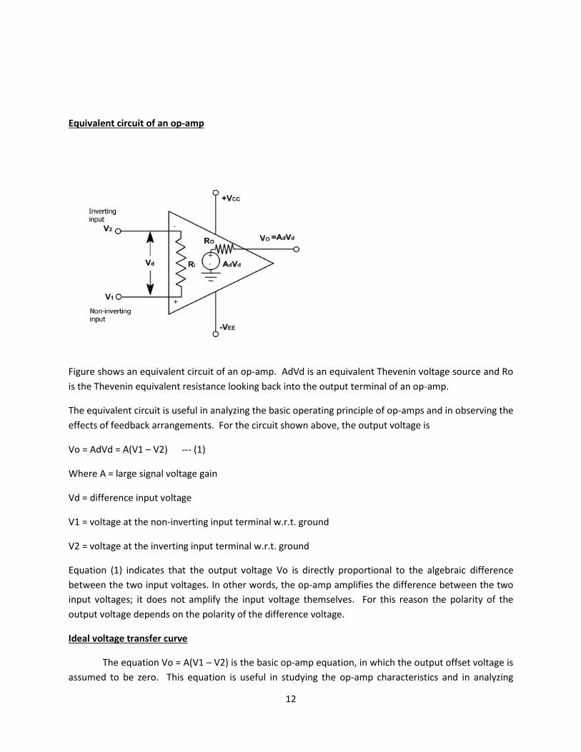
Equivalent circuit of an op-amp
Figure shows an equivalent circuit of an op-amp. AdVd is an equivalent Thevenin voltage source and Ro
is the Thevenin equivalent resistance looking back into the output terminal of an op-amp.
The equivalent circuit is useful in analyzing the basic operating principle of op-amps and in observing the
effects of feedback arrangements. For the circuit shown above, the output voltage is
Vo = AdVd = A(V1 – V2) --- (1)
Where A = large signal voltage gain
Vd = difference input voltage
V1 = voltage at the non-inverting input terminal w.r.t. ground
V2 = voltage at the inverting input terminal w.r.t. ground
Equation (1) indicates that the output voltage Vo is directly proportional to the algebraic difference
between the two input voltages. In other words, the op-amp amplifies the difference between the two
input voltages; it does not amplify the input voltage themselves. For this reason the polarity of the
output voltage depends on the polarity of the difference voltage.
Ideal voltage transfer curve
The equation Vo = A(V1 – V2) is the basic op-amp equation, in which the output offset voltage is
assumed to be zero. This equation is useful in studying the op-amp characteristics and in analyzing

13
different circuit configurations that employ feedback. The graphic representation of this equation is
shown in figure, where the output voltage Vo is plotted against input difference voltage Vid, keeping
gain A constant.
Note that the output voltage cannot exceed the positive and negative saturation voltages. These
saturation voltages are specified by an output voltage swing rating of the op-amp for given values of
supply voltages. This means that the output voltage is directly proportional to the input difference
voltage only until it reaches the saturation voltages and thereafter output voltage remains constant as
shown in figure.
The curve shown above is called an ideal voltage transfer curve. The curve would be almost
vertical because of the very large values of A.
Open Loop Op-amp configurations
Open loop means that there is no connection between input and output terminals (either direct
or via another network). It means that output signal is not feedback in any form to the input. The op-
amp in open loop configuration acts as a high gain amplifier. There are three open loop op-amp
configurations.
1. Differential amplifier
2. Inverting amplifier
3. Non-inverting amplifier
1. Differential amplifier
The circuit of open loop op-amp differential amplifier is shown in figure.

14
In this circuit, inputs are applied to both the inverting and non-inverting terminals. Since, in this
configuration the difference between two input signals is amplified, the configuration is called
the differential amplifier. Source resistances Ri1 and Ri2 are usually negligibly small as
compared to input resistance of op-amp (Rin). Neglecting voltage drop across source resistors.
V1 = Vin1 and V2 = Vin2 and output voltage is given as Vout = A(V1-V2) = A(Vin1 – Vin2), where
A is open loop gain.
2. Inverting amplifier
In inverting configuration, the input signal is applied to the inverting (-) input and non-inverting
(+) input terminal is grounded as shown in figure. Since V1=0 and V2 = Vin, the output voltage
Vout = AVd = A(V1-V2) = -AVin
The negative sign indicates that the output voltage is out of phase w.r.t. input voltage by 180°.
Thus output voltage is A times the input voltage and is of opposite polarity.
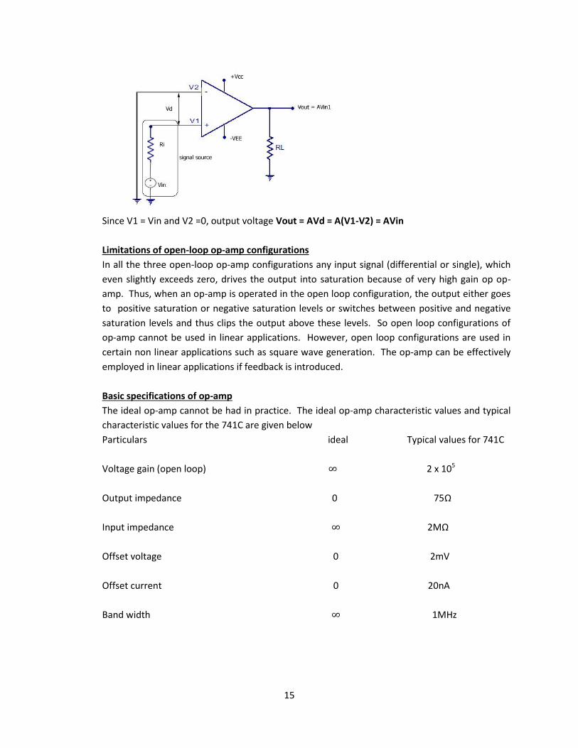
3. Non-inverting amplifier
In this configuration, the input signal is applied to the non-inverting (+) input terminal and
inverting (-) input terminal is grounded.
15
Since V1 = Vin and V2 =0, output voltage Vout = AVd = A(V1-V2) = AVin
Limitations of open-loop op-amp configurations
In all the three open-loop op-amp configurations any input signal (differential or single), which
even slightly exceeds zero, drives the output into saturation because of very high gain op op-
amp. Thus, when an op-amp is operated in the open loop configuration, the output either goes
to positive saturation or negative saturation levels or switches between positive and negative
saturation levels and thus clips the output above these levels. So open loop configurations of
op-amp cannot be used in linear applications. However, open loop configurations are used in
certain non linear applications such as square wave generation. The op-amp can be effectively
employed in linear applications if feedback is introduced.
Basic specifications of op-amp
The ideal op-amp cannot be had in practice. The ideal op-amp characteristic values and typical
characteristic values for the 741C are given below
Particulars ideal Typical values for 741C
Voltage gain (open loop) 2 x 10⁵
Output impedance 0 75Ω
Input impedance 2MΩ
Offset voltage 0 2mV
Offset current 0 20nA
Band width 1MHz

16
Frequency response
The gain of an op-amp is a complex number and is a function of frequency. Therefore,
at a given frequency the gain will have a specific magnitude as well as a phase angle. This means
that the variation in operating frequency will cause the variation in gain magnitude and its phase
angle. The manner in which the gain of the op-amp responds to different frequencies is called
the frequency response. A graph of the magnitude of the gain versus frequency is called a
frequency response curve (plot). Although gain magnitude may be expressed either in decibels
(dB) or as a numerical value, the frequency is always plotted on a logarithmic scale. To
accommodate large frequency ranges the frequency is assigned a logarithmic scale. To
accommodate large frequency ranges the frequency is assigned a logarithmic scale. Similarly
gain magnitude is expressed in decibels to accommodate very high gain. The frequency
response for the amplifier is obtained from the experimental results by measuring its input and
output voltages at different frequencies.
Another technique used in the ac analysis of network is the Bode plot, composed of
magnitude versus frequency and phase angle versus frequency plot. Bode plot is generally used
for stability determination and network design.
Generally for an amplifier, as the operating frequency increases, twp effects become
more evident. (1) The gain of the amplifier decreases and (2) the phase shift between the output

17
and input signals increases. In the case of an op-amp the change in gain and phase shift as a
function of frequency is attributed to the internally integrated capacitors as well as stray
capacitors.
The manner in which the gain of the op-amp changes with variation in frequency is
known as the magnitude plot and the manner in which the phase shift changes with variation in
frequency is known as the phase angle plot.
The rate of change of gain as well as the phase shift can be changed using specific
components with the op-amp. The most commonly used components are resistors and
capacitors. The network formed by such components and used for modifying the rate of change
of gain and the phase shift is called a compensating network. There are two types of op-amps
internally compensated and externally compensated. 741 is an internally compensated op-amp.
The above figure shows the open loop frequency response of an internally compensated
op-amp. The unity gain band width of the 741C is approximately 1MHz. The 741C has a single
break frequency fo before the unity gain bandwidth. The break frequency fo is the -3db
frequency corresponding to 0Hz (dc). The gain of the op-amp remains constant from 0Hz to the
break frequency fo and thereafter rolls off at a constant rate, i.e. 20dB per decade (ten fold
increase in frequency). Thus the open loop band width is the frequency band extending from
0Hz to fo, i.e. 5Hz.
Closed loop frequency response
To increase the band width of an op-amp a negative feedback must be used. The open
loop band width of an op-amp is very small and is about 5Hz. The closed loop band width can
be determined using a frequency response curve. For instance, if the 741C is wired for a gain of
100 or 40dB, its band width will be about 10KHz as shown in the above figure.
Op-amp with negative feedback
The open loop gain of the op-amp is very high. Therefore only smaller signals having
very low frequency can be amplified accurately without distortion. Very small signals are
susceptible to noise and are difficult to obtain in the laboratory. The open loop voltage gain is
not a constant it varies with temperature, power supply voltage and by production itself. The
open loop band width is very small (for 741C it us 5Hz).
We can control the gain of the op-amp by using feedback network. Feed back is the
process of giving a portion of the output back to the input. There are two types of feedback-
positive feedback and negative feedback. If the feedback signal is in phased with the input
signal the feedback is called +ve feedback. On the other hand if the feedback signal is out off
phase (180° phase difference) with the input signal the feedback is called –ve feedback.
Positive feedback is also called regenerative feedback, because it increases the gain.
+ve feedback is used in oscillatory circuit.
Negative feedback is also known as degenerative feedback because it reduces the gain.
–ve feedback stabilizes the gain, increases the band width and changes the input and output
resistances. It also decreases the distortion. –ve feedback reduces the variations in
temperature and power supply voltages on the output of the op-amp.

18
An op-amp that uses feedback is called a feedback amplifier. A feedback amplifier is
sometimes referred to as a closed loop amplifier because the feedback forms a closed loop
between the input and the output. A feedback amplifier essentially consists of two parts: an op-
amp and a feedback circuit. The feedback circuit may be made up of passive components,
active components or combinations of both. There are four types of feedback.
1. Voltage-series feedback
2. Voltage-shunt feedback
3. Current-series feedback
4. Crrrent-shunt feedback

19
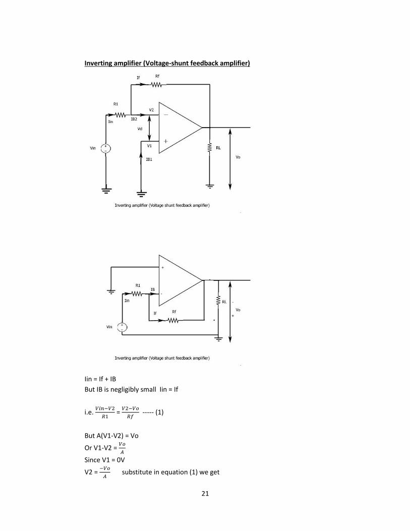
Non inverting amplifier (Voltage –series feedback amplifier)
The above circuit is commonly known as a non-inverting amplifier with feedback.
Open loop voltage gain, A =
Closed loop voltage gain, Af =
Gain of the feedback circuit, β =
In the circuit shown above Vd = Vin – Vf
Vd = difference input voltage
Vin = input voltage
Vf = feedback voltage
20
Closed loop voltage gain
Closed loop voltage gain, Af =
But Vo = A (V1-V2)
V1 = Vin and
V2 = Vf = (
)Vo
Therefore Vo = A(Vin –
) = AVin –AVo
Or Vo+AVo
= AVin
Or Vo(1+A
) = AVin
i.e. Vo(
) = AVin
or Vo =
Thus Af =
=
Generally A is very large (~ 105). Therefore AR1»R1+Rf and R1+Rf+AR1 = AR1
Therefore Af =
=
=
= (1+
)
The gain of the non-inverting amplifier is determined by the ratio of two resistors R1 & Rf.
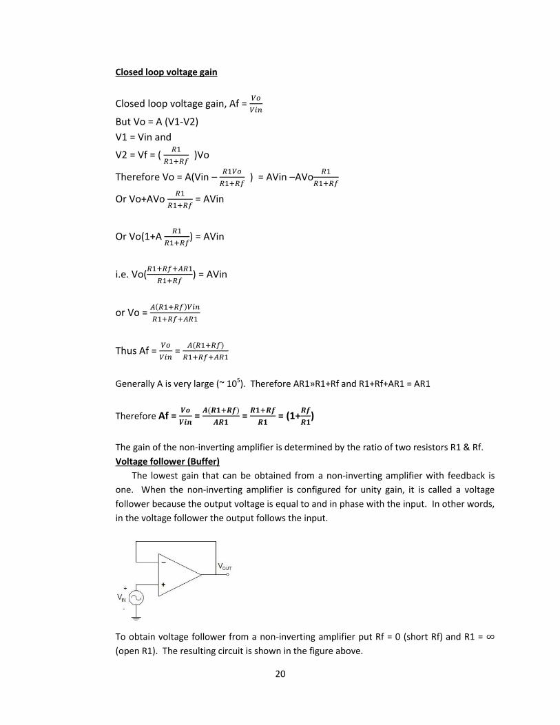
Voltage follower (Buffer)
The lowest gain that can be obtained from a non-inverting amplifier with feedback is
one. When the non-inverting amplifier is configured for unity gain, it is called a voltage
follower because the output voltage is equal to and in phase with the input. In other words,
in the voltage follower the output follows the input.
To obtain voltage follower from a non-inverting amplifier put Rf = 0 (short Rf) and R1 =
(open R1). The resulting circuit is shown in the figure above.
21
Inverting amplifier (Voltage-shunt feedback amplifier)
Iin = If + IB
But IB is negligibly small Iin = If
i.e.
=
----- (1)
But A(V1-V2) = Vo
Or V1-V2 =
Since V1 = 0V
V2 =
substitute in equation (1) we get

22
=
+
=
-
= -Vo (
+
+
)
= -Vo (
)
i.e.
=
=
but closed loop gain
Af =
=
The negative sign shows that the input and output are out off phase by 180°. Since the
internal gain (open loop gain) A is very high
AR1 » (R1 +Rf)
Therefore Af =
=
=
Virtual Ground
Figure (a)
For an ideal op-amp the input resistance is infinite, hence there is no current flow into
either of the input terminals. This characteristic plays an important role in explaining the
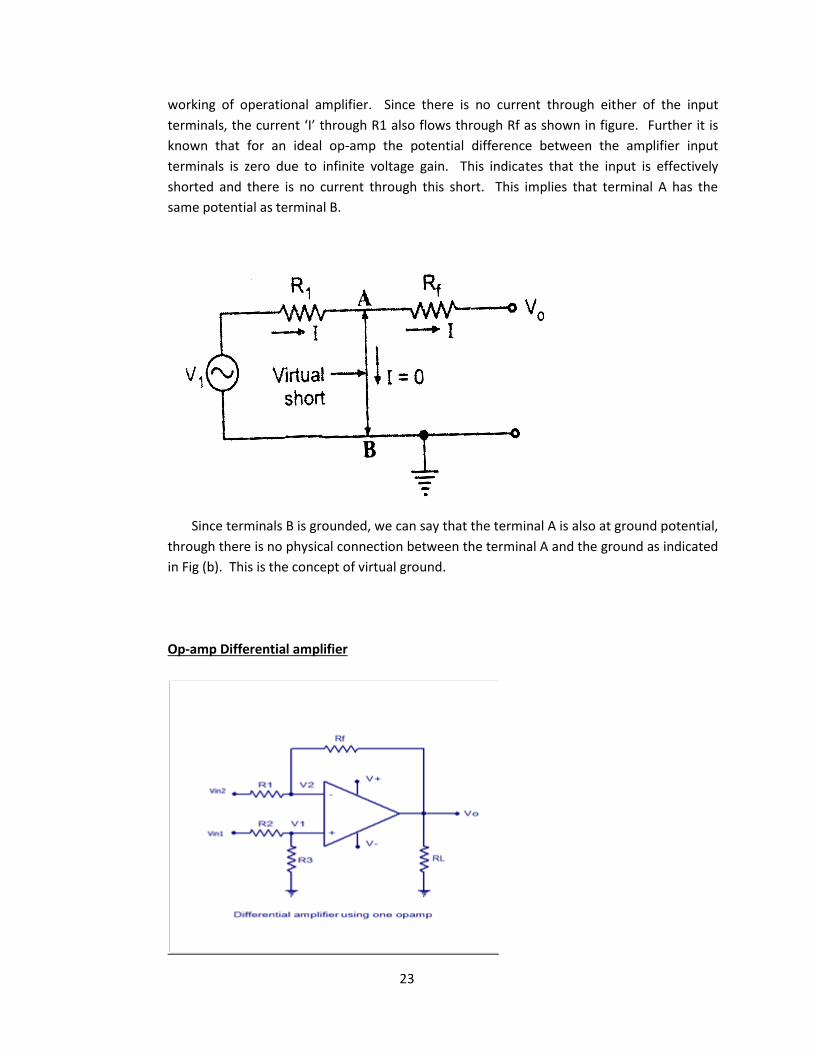
23
working of operational amplifier. Since there is no current through either of the input
terminals, the current ‘I’ through R1 also flows through Rf as shown in figure. Further it is
known that for an ideal op-amp the potential difference between the amplifier input
terminals is zero due to infinite voltage gain. This indicates that the input is effectively
shorted and there is no current through this short. This implies that terminal A has the
same potential as terminal B.
Since terminals B is grounded, we can say that the terminal A is also at ground potential,
through there is no physical connection between the terminal A and the ground as indicated
in Fig (b). This is the concept of virtual ground.
Op-amp Differential amplifier

24
Figure shows a differential amplifier. It is a combination of inverting and non-inverting
amplifiers. When Vin1 is zero, the circuit appears as an inverting amplifier while when Vin2
is zero the circuit becomes a non-inverting amplifier.
Since the circuit has two inputs Vin1 and Vin2, superposition theorem will be used for
determination of voltage gain of the amplifier.
When Vin1 is zero volts, circuit becomes an inverting amplifier and, therefore, output
voltage due to Vin2 is
Vout2 =
Vin2 --- (1)
Now assuming Vin2 = 0, the circuit is a non-inverting amplifier having a voltage divider
network consisting of resistor R2 and R3 at the non-inverting input. Therefore
V1 =
Vin1
And the output due to Vin1 is
Vout1 = (1 +
) V1 = (1 +
) (
) Vin1
If R1 = R2 and Rf = R3
Vout1 = (
) (
) Vin1 =
Vin1 ------(2)
The net output voltage, Vout = Vout1 + Vout2
=
Vin1 -
Vin2
=
(Vin1 – Vin2) =
(Vin2 – Vin1) -----(3)
Differential voltage gain, Ad =
=
The gain of the differential amplifier is same as that of inverting amplifier.
Summing amplifier (Scaling or Averaging)
The most useful op-amp circuits employed in analog computers is the summing
amplifier circuit. This circuit can be used to add ac or dc signals. This circuit provides an output
voltage proportional to or equal to the algebraic sum of two or more input voltages each
multiplied by a constant gain factor. A three input summing circuit is shown in figure below
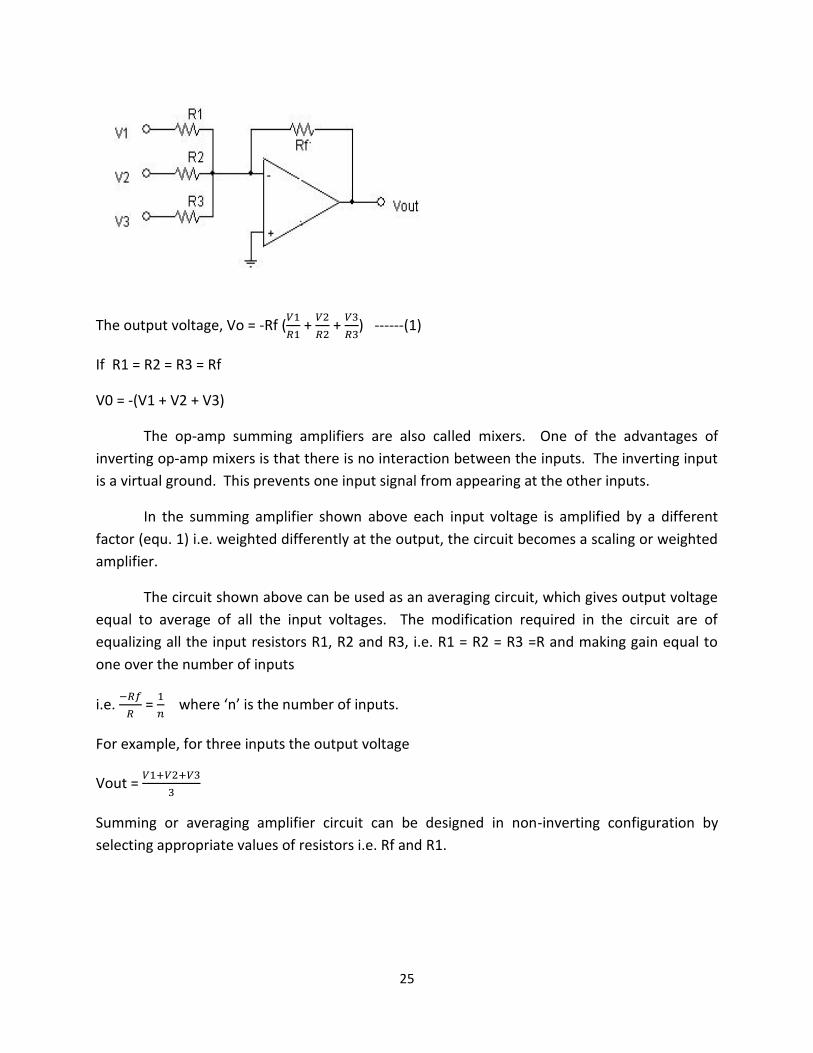
25
The output voltage, Vo = -Rf (
+
+
) ------(1)
If R1 = R2 = R3 = Rf
V0 = -(V1 + V2 + V3)
The op-amp summing amplifiers are also called mixers. One of the advantages of
inverting op-amp mixers is that there is no interaction between the inputs. The inverting input
is a virtual ground. This prevents one input signal from appearing at the other inputs.
In the summing amplifier shown above each input voltage is amplified by a different
factor (equ. 1) i.e. weighted differently at the output, the circuit becomes a scaling or weighted
amplifier.
The circuit shown above can be used as an averaging circuit, which gives output voltage
equal to average of all the input voltages. The modification required in the circuit are of
equalizing all the input resistors R1, R2 and R3, i.e. R1 = R2 = R3 =R and making gain equal to
one over the number of inputs
i.e.
=
where ‘n’ is the number of inputs.
For example, for three inputs the output voltage
Vout =
Summing or averaging amplifier circuit can be designed in non-inverting configuration by
selecting appropriate values of resistors i.e. Rf and R1.

26
The voltage V1 at the non-inverting terminal is
V1 =
Va +
Vb +
Vc =
Hence output voltage is, Vo = (1 +
) (
)
If the gain of the circuit i.e. (1 +
) is made equal to the number of inputs, the output voltage
will become equal to the sum of all the input voltages.
i.e. Vo = Va + Vb + Vc
Summing amplifier in Differential configuration
27
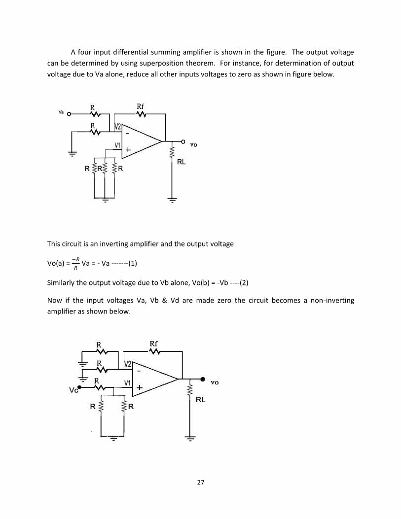
A four input differential summing amplifier is shown in the figure. The output voltage
can be determined by using superposition theorem. For instance, for determination of output
voltage due to Va alone, reduce all other inputs voltages to zero as shown in figure below.
This circuit is an inverting amplifier and the output voltage
Vo(a) =
Va = - Va -------(1)
Similarly the output voltage due to Vb alone, Vo(b) = -Vb ----(2)
Now if the input voltages Va, Vb & Vd are made zero the circuit becomes a non-inverting
amplifier as shown below.

28
The voltage V1 at the non-inverting input terminal is
V1 =
Vc =
So the output voltage due to Vc alone
Vo(c) = (1 +
)V1 = 3(
) = Vc -----(3)
Similarly the output voltage due to Vd alone
Vo(d) = Vd -------(4)
The net output voltage is Vo = Vo(a) + Vo(b) + Vo(c) + Vo(d)
i.e. Vo = -Va – Vb + Vc +Vd ------(5)
The above equation shows that the output voltage is equal to the sum of the input
voltages applied to the non-inverting input terminal plus the negative sum of the input voltages
applied to the inverting input terminal.
The Integrator
An integrator is a circuit that performs a mathematical operation called integration.
Integration is a process of continuous addition. The most popular application of an integrator is
to produce a ramp of output voltage, which is a linearly increasing or decreasing voltage.

29
The integrator is similar to an inverting amplifier except that the feedback is through a
capacitor ‘C’ instead of resistor Rf.
The virtual ground equivalent circuit shows that an expression between input and output
voltage can be derived from the current i, which flows from input to output. The virtual ground
means that the voltage at the junction point of resistor R and capacitor ‘C’ can be considered to
be at ground but no current passes into the ground at that point.
Hence i(t) =
and output voltage
Vo(t) = -
(t) dt = -
dt = -
∫ v(t) dt + A
Where A is the constant of integration and is proportional to the value of the output voltage Vo
at time t = 0 second.
The output voltage is the integral of the input voltage, with an inversion and scale factor of
.
If the input voltage is a step voltage, then the output voltage will be a ramp or linearly changing
voltage. If the input voltage is a square wave, the output voltage will be a triangular wave.
Integrators are widely used in ramp or sweep generators, filters, analog computers etc.

30
A practical integrator is shown below. The resistor Rf limits the low frequency gain and hence
minimizes the variations in the output voltage. The frequency response of the basic integrator
is shown in figure below.
31
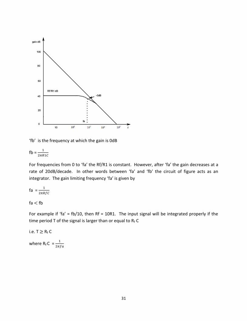
‘fb’ is the frequency at which the gain is 0dB
fb =
For frequencies from 0 to ‘fa’ the Rf/R1 is constant. However, after ‘fa’ the gain decreases at a
rate of 20dB/decade. In other words between ‘fa’ and ‘fb’ the circuit of figure acts as an
integrator. The gain limiting frequency ‘fa’ is given by
fa =
fa fb
For example if ‘fa’ = fb/10, then Rf = 10R1. The input signal will be integrated properly if the
time period T of the signal is larger than or equal to Rf C
i.e. T Rf C
where Rf C =

32
The Differentiator
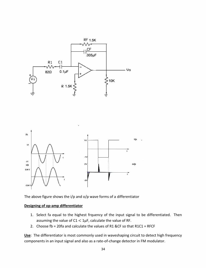
Figure 1
Figure shows the differentiator or differentiation amplifier. The circuit performs the
mathematical operation of differentiation. i.e. The output waveform is the derivative of the
input waveform.
The expression for the output voltage can be obtained from Kirchhoff’s current equation
written at node v2 as
iC = IB + iF
since IB = 0
iC = iF
C1
(vin – v2) =
But v1 = v2 = 0V
C1
=
Or vo = -RF C1
Thus the output ‘vo’ is equal to the RF C1 times the negative instantaneous rate of change of
the input voltage ‘vin’ with time. Since the differentiator performs the reverse of the
integrator’s function, a cosine wave input will produce a sine wave output, or triangular input
will produce a square wave output. The differentiator given above is an unstable one and its
frequency response is shown in the figure below.

33
In this figure ‘fa’ is the frequency at which the gain is 0dB and is given by
fa =
Both the stability and high frequency noise problems in the differentiator shown in Fig (1) can
be corrected by the addition of two components R1 and CF as shown in Fig (3). This circuit is a
practical differentiator, the frequency response of which is shown in Fig (2) by the dotted lines.
Up to frequency ‘fb’ the gain increases at 20dB /decade. After ‘fb’ gain decreases at
20dB/decade. This change in gain is caused by R1C1 and RFCF combinations. The gain limiting
frequency fb is given by
fb =
where R1C1 = RFCF
RFCF and RFCF help to reduce significantly the effect of high frequency input, amplifier noise
and offsets. Above all, it makes the circuit more stable by presenting the increase in gain with
frequency. The value of fb fa
Where fa =
And fb =
=
The input signal will be differentiated properly if the time period T of the input signal is larger
than or equal to RFC1. i.e. T RFC1
34
The above figure shows the i/p and o/p wave forms of a differentiator
Designing of op-amp differentiator
1. Select fa equal to the highest frquency of the input signal to be differentiated. Then
assuming the value of C1 1µF, calculate the value of RF.
2. Choose fb = 20fa and calculate the values of R1 &CF so that R1C1 = RFCF
Use: The differentiator is most commonly used in waveshaping circuit to detect high frequency
components in an input signal and also as a rate-of-change detector in FM modulator.
35
Oscillators
The function of an oscillator is to generate alternating current or voltage waveforms. Or
an oscillator is a circuit that generates a repetitive waveform of fixed amplitude and frequency
without any external input signal.
Oscillator principle
An oscillator is a +ve feedback amplifier. The voltage gain of the amplifier is
=
For an oscillator Vin = 0. Therefore Aβ = 1
The two requirements for oscillation are
1. Aβ 1 (Also known as Barkhausen criterion) and
2. The total phase shift must be equal to 0° or 360° (+ve feedback).
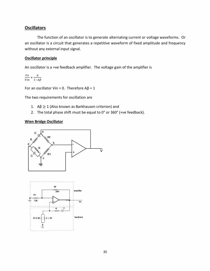
Wien Bridge Oscillator

36
Wien bridge oscillator uses both +ve and –ve feedback. The –ve feedback is used for stability
and the +ve feedback is used for oscillation.
In Wein bridge oscillaator the op-amp is used in the non-inverting mode. The +ve
feedback network in this circuit is a balanced bridge circuit. It consist of a series RC network
and a parallel RC network in two arms of the bridge. The other arms have the resistors R1 and
Rf to form part of the negative feedback.
The phase angle criterion for oscillation is that the total phase shift around the circuit
must be 0°. This condition occurs only when the bridge is balanced, that is at resonance. The
frequency of oscillation fo is exactly the resonant frequency of the balanced Wein bridge and is
given by
fo =
=
(Assume that the resistors are equal in value and capacitors are equal in value in the reactive
leg of the Wein bridge. If they are different then
fo =
)
At this frequency the gain required for sustained oscillation is given by
A = 1/β = 3
i.e. 1 +
= 3
or Rf = 2R1
Colpitt’s Oscillator
Colpitt’s oscillator is widely used in commercial signal generators upto 100MHz.
Colpitt’s oscillator, using an inverting amplifier and a phase shift network consisting of an
inductor and two capacitors is shown in figure.
In this circuit the LC network (L and C1 and C2) provides the required phase shift
between amplifier output voltage and feedback voltage and acts as a filter to pass the desired
oscillating frequency and block all other frequencies.

37
The filter circuit resonates at the desired oscillating frequency. For resonance XL =XC,
where XC is the reactance of the equivalent capacitance in parallel with the inductance. This
provides the resonance or oscillating frequency.
fo =
where C =
=
Consideration of L-C network shows that its attenuation is because of potential divider effect of
L and C2. This gives
It can be shown that for 180° phase shift
XL – XC2 = XC1
So
=
Also A
Or A
38
The resistance of the inductor is negligibly small in comparison to the inductor impedance. i.e.
Q factor (ωL/R) of the inductor is very large.
The capacitors C1 and C2 are ganged. As the tuning is varied, the values of both
capacitors increase or decrease simultaneously, but the ratio of the two capacitances remains
the same.
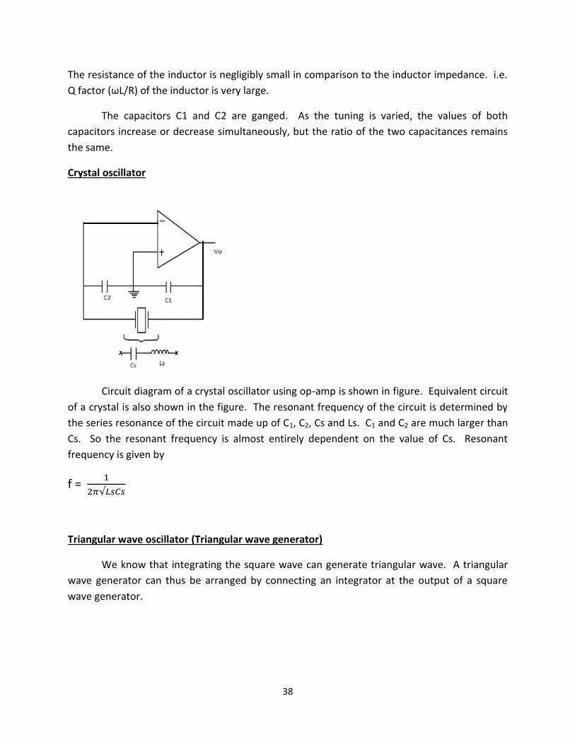
Crystal oscillator
Circuit diagram of a crystal oscillator using op-amp is shown in figure. Equivalent circuit
of a crystal is also shown in the figure. The resonant frequency of the circuit is determined by
the series resonance of the circuit made up of C1, C2, Cs and Ls. C1 and C2 are much larger than
Cs. So the resonant frequency is almost entirely dependent on the value of Cs. Resonant
frequency is given by
f =
Triangular wave oscillator (Triangular wave generator)
We know that integrating the square wave can generate triangular wave. A triangular
wave generator can thus be arranged by connecting an integrator at the output of a square
wave generator.

39
The circuit diagram of a triangular wave oscillator is shown in figure. Here the first op-amp
forms a square wave generator and is followed by a second op-amp, which act as an integrator.
Assume that Vl is at +Vsat. This forces a constant current (+Vsat/R3) through C2 to drive Vo
negative linearly. When Vl is low at –Vsat, it forces a constant current (-Vsat/R3) through C2 in
opposite direction to drive Vo positive linearly as shown in figure.
The frequency of the triangular wave is same as that of the square wave. Although the
amplitude of the square wave is constant ( Vsat), the amplitude of the triangular wave
decreases with an increase in its frequency and vice versa. This is because the reactance of the
capacitors decreases at high frequencies and increases at low frequencies
40
Vo(p-p) =
The output of the integrator will be triangular wave only when 5R4C2 T/2, where T is the time
period of the square wave. As a general rule R3C2 should be equal to T.
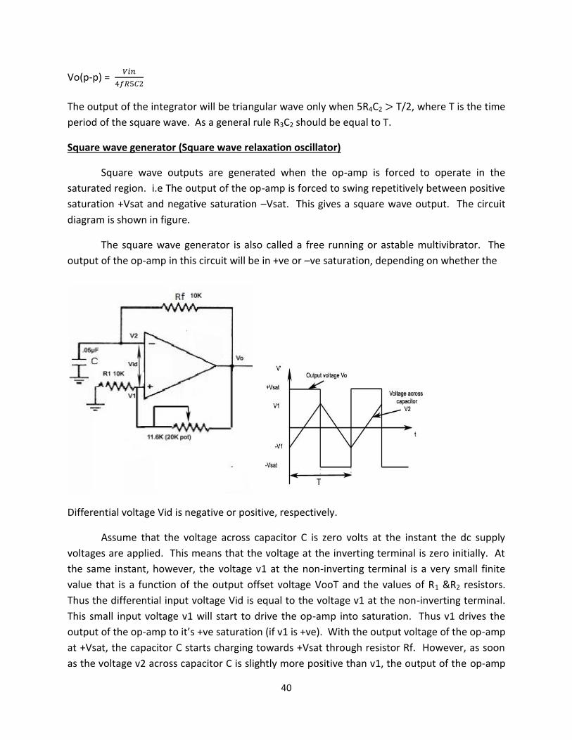
Square wave generator (Square wave relaxation oscillator)
Square wave outputs are generated when the op-amp is forced to operate in the
saturated region. i.e The output of the op-amp is forced to swing repetitively between positive
saturation +Vsat and negative saturation –Vsat. This gives a square wave output. The circuit
diagram is shown in figure.
The square wave generator is also called a free running or astable multivibrator. The
output of the op-amp in this circuit will be in +ve or –ve saturation, depending on whether the
Differential voltage Vid is negative or positive, respectively.
Assume that the voltage across capacitor C is zero volts at the instant the dc supply
voltages are applied. This means that the voltage at the inverting terminal is zero initially. At
the same instant, however, the voltage v1 at the non-inverting terminal is a very small finite
value that is a function of the output offset voltage VooT and the values of R1 &R2 resistors.
Thus the differential input voltage Vid is equal to the voltage v1 at the non-inverting terminal.
This small input voltage v1 will start to drive the op-amp into saturation. Thus v1 drives the
output of the op-amp to it’s +ve saturation (if v1 is +ve). With the output voltage of the op-amp
at +Vsat, the capacitor C starts charging towards +Vsat through resistor Rf. However, as soon
as the voltage v2 across capacitor C is slightly more positive than v1, the output of the op-amp
41
is forced to switch to a negative saturation –Vsat. With the op-amp’s output voltage at –ve
saturation, -Vsat, the voltage v1 across R1 is also negative
V1 =
(-Vsat)
Thus the net differential voltage vid = v1 –v2 is negative, which holds the output of the op-amp
in negative saturation. The output remains in negative saturation until the capacitor C
discharges and then recharges to a negative voltage slightly higher than –v1. Now as soon as
the capacitor’s voltage v2 becomes more negative than –v1, the net differential voltage vid
becomes +ve and hence drives the output of the op-amp back to its positive saturation +Vsat.
This completes one cycle. With output at +Vsat, voltage v1 at the non-inverting input is
V1 =
(+Vsat)
The time period T of the output waveform is given by
T = 2RfC ln (
)
fo =
If R2 = 1.16R1
fo =
This equation shows that smaller the RfC time constant, the higher the output frequency fo and
vice versa.
Saw tooth wave generator
The difference between the triangular and saw tooth waveforms is that in triangular
waves the rise time is always equal to its fall time while the saw tooth waveform have different
rise and fall times.
The circuit shown (below) provides the ability of controlling ramp generation with an
external signal. In the circuit show an npn transistor has been placed around the charging
capacitor C and emitter of the transistor is tied to the inverting terminal of the op-amp, which is
at virtual ground. Resistor RB is for limiting the base current and so for protecting the
transistor. However, RB is to be kept relatively small to ensure that the transistor can be driven
into saturation.

42
. With a zero or negative control input voltage, the transistor is off. The capacitor charges
up from the op-amp output, through C, Rin and to V--. The charge rate is given as
Rate =
If the control voltage is not changed, the capacitor C will eventually charge up, and hold the
output at +Vsat.
However, when a positive control input is applied, the transistor gets turned on. If this voltage
is large enough to force transistor into saturation the capacitor is effectively short circuited.
The capacitor C rapidly discharges.
The output voltage falls to zero (about 0.2V) and stays there as long as positive control voltage
keeps the transistor saturated.
43
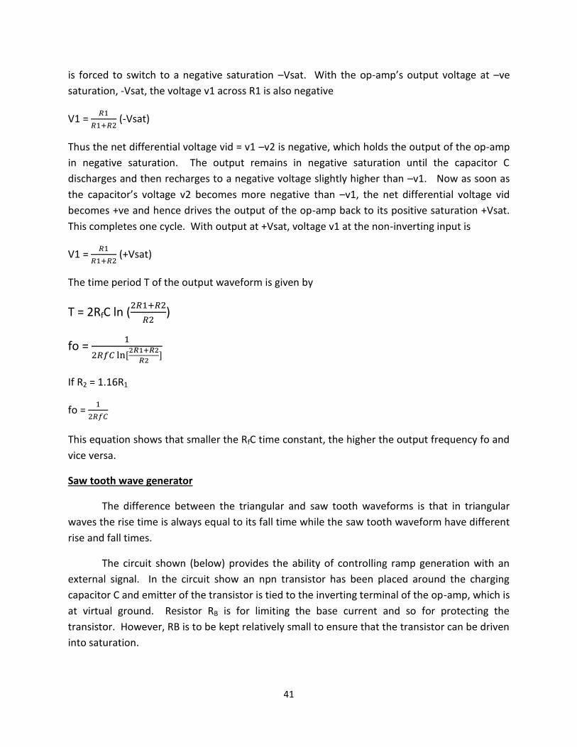
The control input and output wave form are shown in figure. To get negative going ramp:-
1. Reverse the charging voltage V+ connected to Rin.
2. Reverse the capacitor, if it is an electronic one.
3. Replace the npn transistor to a pnp transistor.
Comparators
The comparator is a circuit that is used to compare two voltages and provide an output
indicating the relationship between those two voltages. Comparators are used to compare
1. Two changing voltages to each other, as in comparing two sine waves or
2. A changing voltage to a set dc reference voltage.
Figure shows the circuit of an op-amp comparator. There is no feedback path in the circuit. In
this circuit, the input voltage is applied to the non-inverting input terminal and a set reference
voltage (Vref) is applied to the inverting terminal of the op-amp.

44
F
Figure 1. Figure 2.
As long as the input voltage is below Vref, the comparator output is
approximately –Vmax volts. But if the input voltage equals Vref or exceeds it, the comparator
output changes to +Vmax volts. Thus depending upon the value of input voltage, the
comparator produces a dc voltage that indicates the polarity (or magnitude) relationship
between the two input voltages as shown in Figure 2.
If the reference input (inverting input) of the op-amp is grounded (Vref =
0) and the input signal voltage is applied to the non-inverting input. The output of the op-amp
is equal to –Vmax when the input signal is –ve and the output become +Vmax when the input
signal equal to or greater than zero. Such a circuit is called zero level detectors. This can be
used as a squaring circuit to produce a square wave from a sine wave.
Audio amplifier
In communication receivers, the final output stage is the audio amplifier. The ideal
audio amplifier will have the following characteristics.
1. High gain
2. Minimum distortion in the audio frequency range
3. High input resistance
4. Low output resistance to provide optimum coupling to the speaker.
The above requirements can be fulfilled by using op-amp in an audio amplifier. The op-
amp audio amplifier is shown in figure.

45
The op-amp is supplied only from +V volt power supply, the –V terminal is grounded.
Because of this the output will be between the limits of (+V – 1)volt and +1 volt approximately.
The capacitor Cc2 is used to reference the speaker signal around ground. The capacitor Cs is
included in the Vcc line to prevent any transient current caused by the operation of op-amp
from being coupled back to Q1 through the power supply. The high gain requirement is
accomplished by the combination of two amplifier stages. The high Rin/low Rout of the audio
amplifier is accomplished by the op-amp itself.
High Impedance Voltmeter
46
Figure shows the circuit of a high impedance voltmeter. In such a circuit, the closed
loop gain depends on the internal resistance of the meter, RM. The input voltage will be
amplified and the output voltage will cause a proportional current to flow through the meter.
By adding a small series potentiometer in the feedback loop, the meter can be calibrated to
provide a more accurate reading.
The high input impedance of the op-amp reduces the circuit loading that is caused by
the use of the meter. Although this type of circuit would cause some circuit loading, it would
be much more accurate than a VOM (volt-ohm meter) with an input impedance of 20KΩ/V.
Active Filters
The tuned amplifier circuits using op-amp are generally referred to as active filters. The
frequency response of the circuit is determined by resistor and capacitor values.
Passive filter can be constructed by using passive components like resistors and
capacitors. But in active filter in addition to passive components (resistors and capacitors) an
amplifier using op-amp is also used. The amplifier in the active filter circuit may provide voltage
amplification and signal isolation or buffering.
There are four major types of filter namely, low-pass filter, high- pass filter, band-pass
filter and band- stop filter or notch filter.
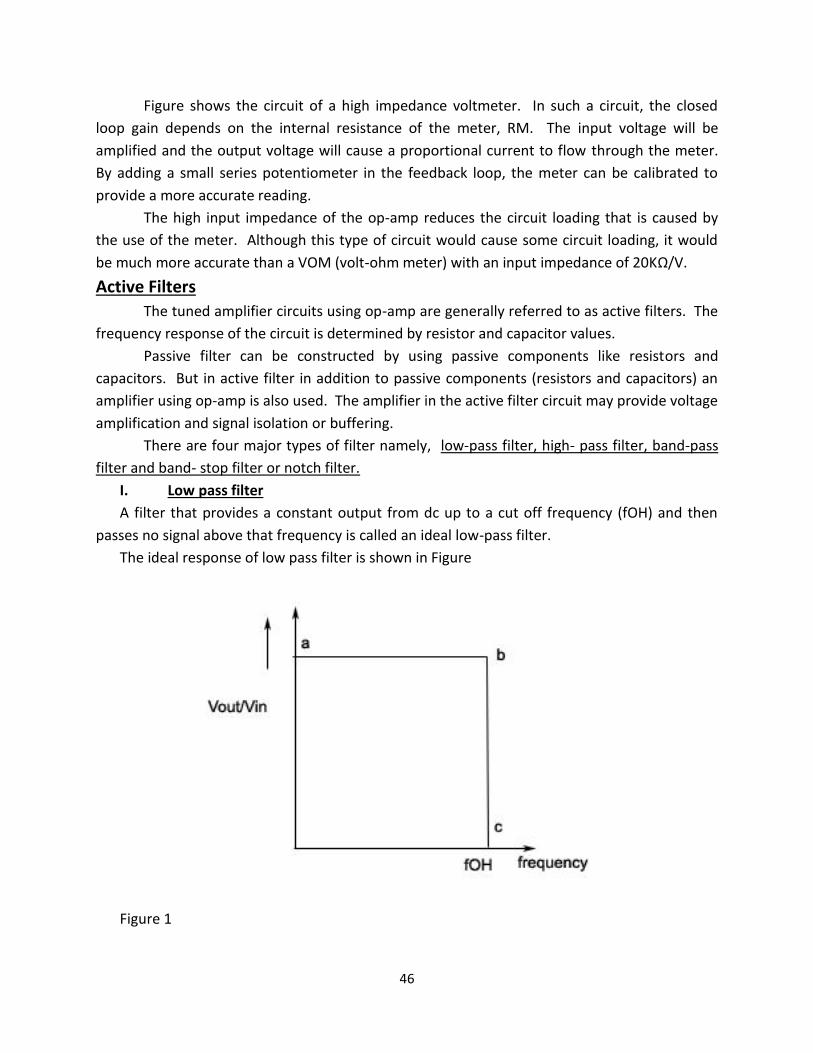
I. Low pass filter
A filter that provides a constant output from dc up to a cut off frequency (fOH) and then
passes no signal above that frequency is called an ideal low-pass filter.
The ideal response of low pass filter is shown in Figure
Figure 1
47
The response shows that the filter has a constant output (ab) from dc up to cut off
frequency fOH. Beyond fOH output becomes zero (bc).
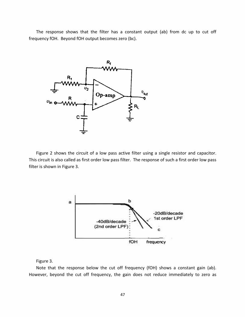
Figure 2 shows the circuit of a low pass active filter using a single resistor and capacitor.
This circuit is also called as first order low pass filter. The response of such a first order low pass
filter is shown in Figure 3.
Figure 3.
Note that the response below the cut off frequency (fOH) shows a constant gain (ab).
However, beyond the cut off frequency, the gain does not reduce immediately to zero as
48
expected in Figure 1, but reduces with a slope of 20dB/decade. The voltage gain for a low pass
filter below the cut off frequency (fOH) is given by the relation
Av = 1 +
And the cut off frequency
fOH =
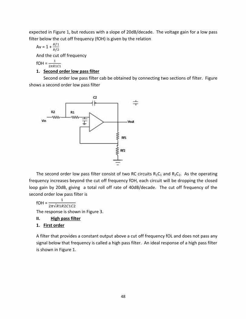
1. Second order low pass filter
Second order low pass filter cab be obtained by connecting two sections of filter. Figure
shows a second order low pass filter
The second order low pass filter consist of two RC circuits R1C1 and R2C2. As the operating
frequency increases beyond the cut off frequency fOH, each circuit will be dropping the closed
loop gain by 20dB, giving a total roll off rate of 40dB/decade. The cut off frequency of the
second order low pass filter is
fOH =
The response is shown in Figure 3.
II. High pass filter
1. First order
A filter that provides a constant output above a cut off frequency fOL and does not pass any
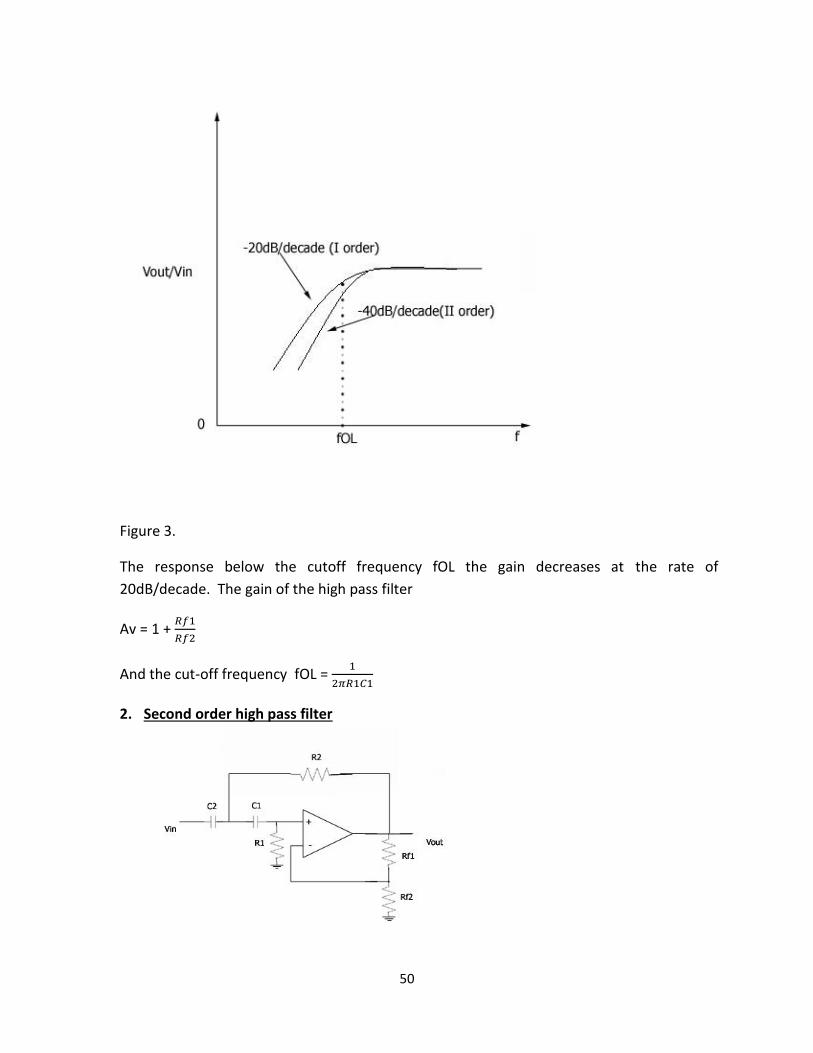
signal below that frequency is called a high pass filter. An ideal response of a high pass filter
is shown in Figure 1.

49
The output become zero from dc to fOL (oa) and a constant output above fOL (bc).
Figure 2.
Figure 2 shows the circuit of a first order high pass filter using a single resistor and
capacitor. The response of a practical 1st order high pass filter is shown in Figure 3.
50
Figure 3.
The response below the cutoff frequency fOL the gain decreases at the rate of
20dB/decade. The gain of the high pass filter
Av = 1 +
And the cut-off frequency fOL =
2. Second order high pass filter
51
Second order high pass filter can be obtained by connecting two sections of filters. The
second order high pass filter consist of two RC circuits R1C1 and R2C2. As the operating
frequency decreases below fOL each RC circuit will be dropping the closed loop gain by
20dB, giving a total roll off rate of 40dB/decade. The output frequency of the second
order low pass filter s
fOL =
The response of 2nd order high pass filter is shown in Figure 3.
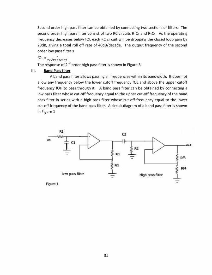
III. Band Pass filter
A band pass filter allows passing all frequencies within its bandwidth. It does not
allow any frequency below the lower cutoff frequency fOL and above the upper cutoff
frequency fOH to pass through it. A band pass filter can be obtained by connecting a
low pass filter whose cut-off frequency equal to the upper cut-off frequency of the band
pass filter in series with a high pass filter whose cut-off frequency equal to the lower
cut-off frequency of the band pass filter. A circuit diagram of a band pass filter is shown
in Figure 1
52
Figure 2
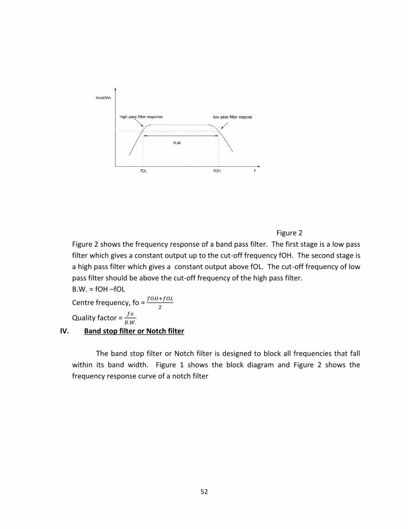
Figure 2 shows the frequency response of a band pass filter. The first stage is a low pass
filter which gives a constant output up to the cut-off frequency fOH. The second stage is
a high pass filter which gives a constant output above fOL. The cut-off frequency of low
pass filter should be above the cut-off frequency of the high pass filter.
B.W. = fOH –fOL
Centre frequency, fo =
Quality factor =
IV. Band stop filter or Notch filter
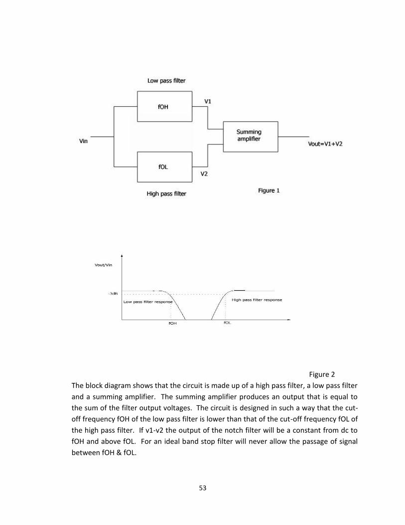
The band stop filter or Notch filter is designed to block all frequencies that fall
within its band width. Figure 1 shows the block diagram and Figure 2 shows the
frequency response curve of a notch filter
53
Figure 2
The block diagram shows that the circuit is made up of a high pass filter, a low pass filter
and a summing amplifier. The summing amplifier produces an output that is equal to
the sum of the filter output voltages. The circuit is designed in such a way that the cut-
off frequency fOH of the low pass filter is lower than that of the cut-off frequency fOL of
the high pass filter. If v1-v2 the output of the notch filter will be a constant from dc to
fOH and above fOL. For an ideal band stop filter will never allow the passage of signal
between fOH & fOL.
54
CHAPTER 2
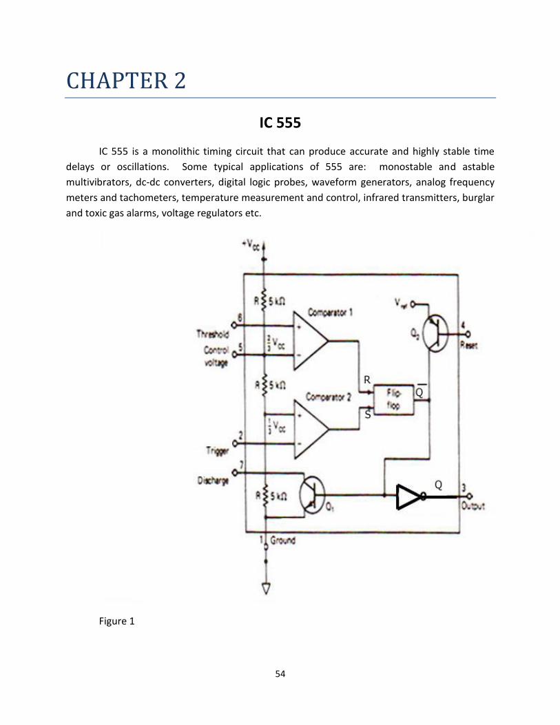
IC 555
IC 555 is a monolithic timing circuit that can produce accurate and highly stable time
delays or oscillations. Some typical applications of 555 are: monostable and astable
multivibrators, dc-dc converters, digital logic probes, waveform generators, analog frequency
meters and tachometers, temperature measurement and control, infrared transmitters, burglar
and toxic gas alarms, voltage regulators etc.
Figure 1

55
Figure-2
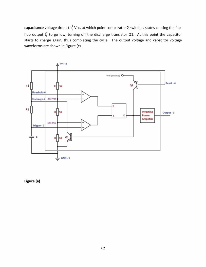
The figure-1 shows the functional diagram of SE/NE 555 timer. Figure-2 shows the pin
configuration of IC 555. The IC 555 consist of two comparators that drives the set(S) and reset
(R) terminals of a flip-flop, which in turn controls the ‘on’ and ‘off’ cycles of the discharge
transistor Q1. The comparator reference voltages are fixed at 2/3Vcc for comparator 1 and
Vcc/3 for comparator 2, by means of the voltage divider made up of three series resistors (R).
These reference voltages are required to control the timing. The timing can be controlled
externally by applying voltage to the control voltage terminal. If no such control is required
then the control voltage terminal can be bypassed by a capacitor to ground. Typically the
capacitor chosen is about 0.01µF.
On a negative transition of pulse applied at the trigger terminal and when the
voltage at the trigger terminal passes through Vcc/3, the output of comparator 2 changes state
because its positive input terminal is fixed at Vcc/3. This change of state sets the flip-flop, so
that output of flip-flop, , goes to low level. On the other hand when the voltage applied at the
threshold terminal of comparator 1 goes positive and passes through the reference level
2/3Vcc, the output of the comparator changes its state. This change of state resets the flip-flop,
so that is latches into high level. A separate reset terminal is provided for timer which is used
to reset the flip-flop externally. This reset voltage applied externally would override the effect
of the output of lower comparator which sets the flip-flop. This overriding reset will be in effect
whenever the reset input is less than about 10.4 Volts. Normally, when the reset terminal is
56
not used, it should be connected to positive supply (Vcc). The transistor Q2 act as a buffer,
isolating the reset terminal from the flip-flop and transistor Q1. The output of the flip –flop is
which is also used as an output terminal taken through an output stage or buffer. When the
flip-flop is reset, the output at the output terminal is low and when the flip-flop is set the
output is in high logic state. The buffer is necessary to source current as high as 200mA. A
capacitor is connected between the discharge terminal and ground. When Q1, is OFF the
capacitor charges and when Q1 is ON it discharges through Q1.
Pin functions of 8 pin DIP 555
Pin 1: Ground:- All voltages are measured with respect to this terminal.
Pin 2: Trigger:- The output of the timer depends on the amplitude of the external
trigger pulse applied to this pin. The output is low when the trigger is 1/3Vcc. When a
negative going pulse of amplitude greater than 1/3Vcc the output goes high.
Pin 3: Output:- There are two ways a load can be connected to the output terminal :
either between pin3 and ground (pin1) or between pin 3 and supply voltage +Vcc (pin 8).
When the output is low, the load current passes through the load connected between
pin 3 and +Vcc into the output terminal and is called the sink current. However, the current
through the grounded load is zero, when the output is low. For this reason, the load connected
between pin 3 and +Vcc is called the normally ON load and that between pin 3 and ground is
called the normally OFF load. On the other hand, when the output is high, the current through
the load connected between pin 3 and +Vcc (normally on load) is zero. However, the output
terminal supplies current to the normally OFF load. This current is source current. The
maximum value of sink or source current is 200mA.
Pin 4: Reset:- The device 555 is reset (disabled) by applying a negative pulse to this pin
when the reset function is not in use, the reset terminal should be connected to +Vcc to avoid
any possibility of false triggering.
Pin 5: Control voltage:- An external voltage applied to this terminal changes the
threshold as well as the trigger voltage. In other words, by imposing a voltage on this pin or by
connecting a potentiometer between this pin and ground, the pulse width of the output
waveform can be varied. When not used, the control pin should be bypassed to ground with a
0.01µF capacitor to prevent any noise disturbances.
Pin 6: Threshold:- This is the non-inverting terminal of comparator C1, which monitors
the voltage across the external capacitor. When the voltage at this pin is greater than or equal
57
to
Vcc, the output of comparator C1 goes high, which in turn switches the output of the timer
low.
Pin 7: Discharge:- This pin is connected internally to the collector of transistor Q1.
When the output is high Q1 is off and act as an open circuit to the external capacitor connected
between pin 7 and ground. On the other hand, when the output is low, Q1 is saturated and act
as a short circuit, shorting out the external capacitor C to ground.
Pin 8: +Vcc :- The supply voltage of +5V to +18 V is applied to this pin with respect to
ground (pin 1).
Timer 555 – Monostable operation
The circuit in Figure 1 is connected as a monostable multivibrator, the resistance RA and
the capacitor C are external to the chip, and their values determine the output pulse width.
The three equal resistances R, inside the chip, establish the reference voltages
Vcc and
Vcc
for comparators 1 and 2 of timer respectively. The value of R cannot be controlled precisely.
However, IC fabrication techniques control resistance ratios accurately so that reference
voltages are precise.

58
Figure 1
Before the application of the trigger pulse Vin(t) (Figure 1), the voltage at the trigger
input pin is high which is equal to Vcc. With this high trigger input, the output of comparator 2
will be low, causing the flip-flop output to be high, and Vo =0 (due to inverter circuit). With
high, the discharge transistor Q1 will be saturated and the voltage across the timing capacitor C
will be essentially zero (Vc(t) = 0). The output Vo = 0V is the quiescent state of the timer device.
At t=0, application of trigger Vin(t) (-ve going pulse shown in Fig 2) less than
Vcc, causes
the output of comparator 2 to be high. This will set the flip-flop with now low. This makes
Vo high. Due to low, discharge transistor will be turned ‘off’. Note that after termination of
the trigger pulse the flip-flop will remain in the low state. Now, the timing capacitor charges
up towards Vcc via resistor R, with a time constant Ԏ = RAC.

59
Figure 2
The charging up expression is
Vc(t) = Vcc (1 - ) -----(1)
Where vc(t) is the voltage across C at any time ‘t’.
When vc(t) reaches the threshold voltage level of
Vcc, comparator 1 will switch state
and its output voltage will now be high. This causes the flip-flop to reset so that will go high
and Vo returns to original level low. The high value of turns on the discharge transistor Q1.
The low saturation resistance of Q1 discharges C quickly.
The end of the output pulse occurs at time T1, at which point Vc(t) =
Vcc. Thus the
pulse width T1 is determined by the time required for the capacitor voltage Vc(t) to charge
from zero to
Vcc. This period can be obtained by putting Vc(t) =
Vcc at t = T1 in Equation (1)
i.e.
Vcc = Vcc (1 - )
so T1 = RAC ln (
)
60
or T1 = 1.1 RC ----(2)
The trigger pulse must be shorter in duration than T1 for proper operation of the timer.
A decoupling capacitor (10µF) may be connected between pin 8 and pin 1 to eliminate
unwanted voltage spikes in the output waveform.
Sometimes, to prevent any possibility of mis-triggering the monostable multivibrator on
positive pulse edges, a wave shaping circuit consisting of R1, C1 and diode D is connected
between the trigger input (pin 2) and Vcc (pin 8) as shown in figure. The value of R1 and C1
should be selected so that the time constant R1C1 is smaller than the output pulse width T1.
The monstable timing period can be varied by voltage applied to the control terminal.
Design considerations
The practical value of RA (figure 1 or 2 above) range from 2KΩ to well into the MΩ range.
The minimum value of the timing capacitor C is approximately 500PF, its maximum value is
determined by the quality of the capacitor used, but is generally less than 2000µF. The
maximum value of RA is
RA(max)
The minimum value of RA is 1KΩ
Monostable multivibrator Applications
(i) Frequency Divider
The monostable multivibrator can be used as a frequency divider by adjusting the length of
the timing cycle T1 with respect to the time period T of the trigger input signal applied to pin 2.
To use the monostable multivibrator as a divide by 2 circuit, the timing interval T1 must be
slightly larger than the time period T of the trigger input signal, as shown in Figure 3.

61
By the same concept, to use the monostable multivibrator as a divide by 3 circuit, T1 must be
slightly larger than twice the period of the input trigger signal.
The frequency divider application is possible because the monostable multivibrator cannot be
triggered during the timing cycle.
Figure 3
(ii) Pulse Stretcher
Since we find that the output pulse width of monostable multivibrator is of
longer duration than the negative pulse width of the input trigger, the output
pulse can be considered as a stretched version of the narrow input
Timer 555 used in Astable mode
Figure (a) shows the 555 timer connected as an astable multivibrator. In this mode of
operation, the timing capacitor charges up towards Vcc through R1 and R2 until the voltage
across the capacitor reaches the threshold level of
Vcc. At this point comparator 1 switches
state causing the flip-flop output to go high. This turns on the discharge transistor Q1 and
the timing capacitor C then discharges through R2 and Q1. The discharging continues until the
62
capacitance voltage drops to
Vcc, at which point comparator 2 switches states causing the flip-
flop output to go low, turning off the discharge transistor Q1. At this point the capacitor
starts to charge again, thus completing the cycle. The output voltage and capacitor voltage
waveforms are shown in Figure (c).
Figure (a)
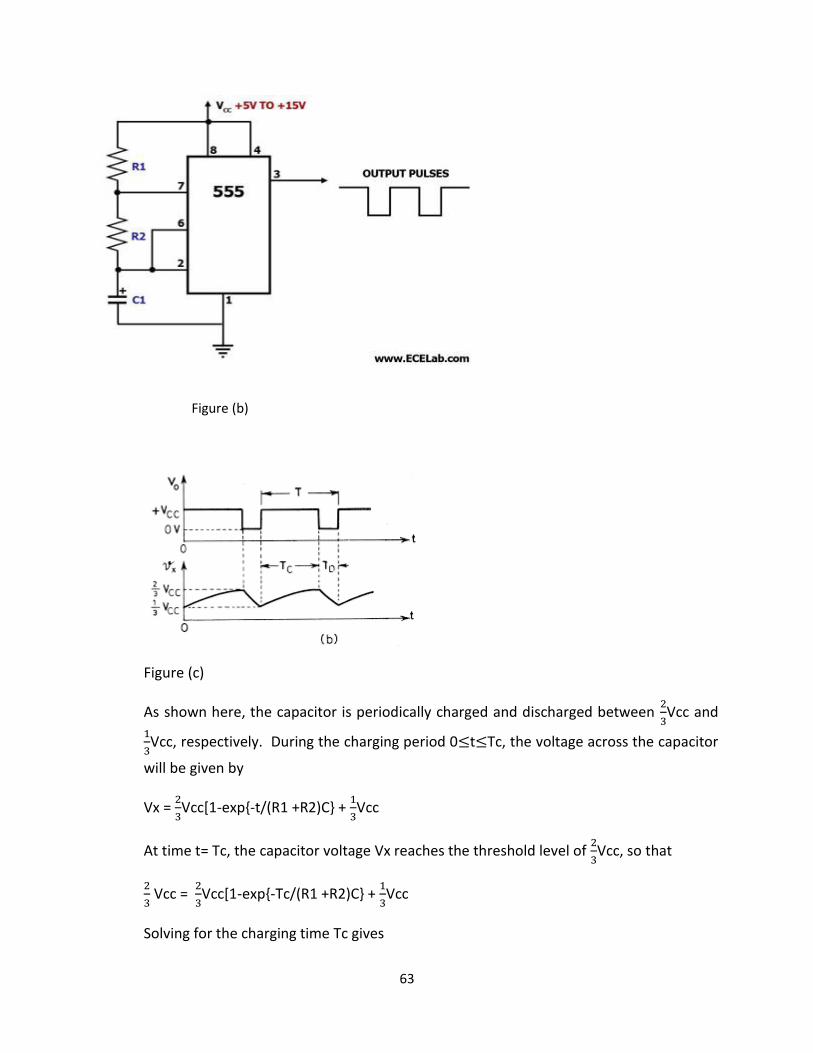
63
Figure (b)
Figure (c)
As shown here, the capacitor is periodically charged and discharged between
Vcc and
Vcc, respectively. During the charging period 0 t Tc, the voltage across the capacitor
will be given by
Vx =
Vcc[1-exp-t/(R1 +R2)C +
Vcc
At time t= Tc, the capacitor voltage Vx reaches the threshold level of
Vcc, so that
Vcc =
Vcc[1-exp-Tc/(R1 +R2)C +
Vcc
Solving for the charging time Tc gives

64
Tc = (R1 +R2)C ln2 = 0.693 (R1 +R2)C
During the discharge interval 0 TD we have that
Vx =
Vcc exp(-t1/R2C)
At time t1 = TD, the voltage across the capacitor reaches the trigger level of
Vcc, so we
have
Vcc =
Vcc exp(-TD/R2C)
Solving for TD, we obtain
TD = R2C ln2 = 0.693R2 C
Where TD is the discharge time. The total period T = Tc + TD and is given as
T = 0.693(R1 + 2R2)C
And the frequency of oscillation will be
fo =
=
=
The frequency fo is independent of Vcc. The duty cycle of the output waveform is given
by
d% =
x 100 =
x 100
The duty cycle will always be greater than 50% for this circuit.
To achieve 50% duty cycle we should make R1 = 0Ω, which will damage Q1.
Square wave oscillator
The circuit producing 50% duty cycle is achieved by connecting a diode D across
resistor Rb as shown in Fig (d). Astable multivibrator with 50% duty cycle is also known
as square wave oscillator.

65
In this circuit the capacitor C charges through Ra and diode D, to approximately
Vcc
and discharges, through Rb and Q1, until the capacitor voltage equals approximately
Vcc, then
the cycle repeats.
To obtain a square wave output Ra must be a combination of a fixed resistor and
potentiometer so that the potentiometer can be adjusted for the exact square wave.
Voltage controlled oscillator

66
The circuit is sometimes called a voltage-to-frequency converter because the output
frequency can be changed by changing the input voltage.
The pin 5 terminal is voltage control terminal and its function is to control the threshold and
trigger levels. Normally, the control voltage is +2/3VCC because of the internal voltage divider.
However, an external voltage can be applied to this terminal directly or through a pot, as illustrated in
figure, and by adjusting the pot, control voltage can be varied. Voltage across the timing capacitor is
shown in figure, which varies between +Vcontrol and ½ Vcontrol. If control voltage is increased, the
capacitor takes a longer to charge and discharge; the frequency, therefore, decreases. Thus the fre-
quency can be changed by changing the control voltage. Incidentally, the control voltage may be
made available through a pot, or it may be output of a transistor circuit, op-amp, or some other
device.
Design considerations for Astable operation
The duty cycle, d, can be selected between 60% to 90%. The value of timing capacitor C can be
selected between 500pF and 1000µF. For a given duty cycle d, frequency fo and C, the Ra and
Rb are selelcted using following equations.
Ra =
Generally 1KΩ Ra 3.3MΩ
And Rb =
Where 1KΩ Rb 3.5MΩ
Bypass capacitor C1 and C2 range between 0.1 and 10µF. Disc ceramic or tantalum capacitors
should be used. The timing capacitor should be silver mica, polyhstyrene, tantalum, or mylar
for best result. Also, the timing capacitor leakage should be much less than available charging
current.
Pin 5 can be used to vary the timing as a function of control voltage. As a guide, the control
voltage should be between 0.45 Vcc and 0.9 Vcc.
67
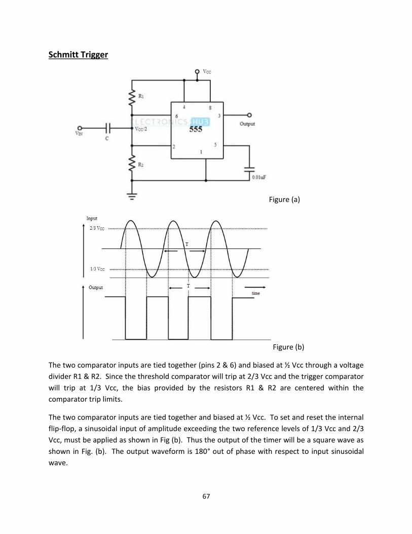
Schmitt Trigger
Figure (a)
Figure (b)
The two comparator inputs are tied together (pins 2 & 6) and biased at ½ Vcc through a voltage
divider R1 & R2. Since the threshold comparator will trip at 2/3 Vcc and the trigger comparator
will trip at 1/3 Vcc, the bias provided by the resistors R1 & R2 are centered within the
comparator trip limits.
The two comparator inputs are tied together and biased at ½ Vcc. To set and reset the internal
flip-flop, a sinusoidal input of amplitude exceeding the two reference levels of 1/3 Vcc and 2/3
Vcc, must be applied as shown in Fig (b). Thus the output of the timer will be a square wave as
shown in Fig. (b). The output waveform is 180° out of phase with respect to input sinusoidal
wave.

68
The important characteristic of the Schmitt trigger is Hysteresis. The output of the Schmitt
trigger is high if the input voltage is greater than the upper threshold value and the output of
the Schmitt trigger is low if the input voltage is lower than the lower threshold value.
The output retains its value when the input is between the two threshold values. The usage of
two threshold values is called Hysteresis and the Schmitt trigger acts as a memory element (a
bistable multivibrator or a flip-flop).
The threshold values in this case are 2/3 VCC and 1/3 VCC i.e. the upper comparator trips at 2/3
VCC and the lower comparator trips at 1/3 VCC. The input voltage is compared to these
threshold values by the individual comparators and the flip-flop is SET or RESET accordingly.
Based on this the output becomes high or low.
When a sine wave of amplitude greater than VCC / 6 is applied at the input, the flip-flop is set
and reset alternately for the positive cycle and the negative cycle. The output is a square wave
and the waveforms for input sine wave and output square wave are shown above (Figure b).
Bistable multivibrator using IC 555
In bistable mode the 555 timer act as a basic flip-flop. The trigger and reset inputs (2 &4) are
connected to +Vcc via resistors while the threshold input (6) is simply grounded. To set the
multivibrator (o/p high) connect the trigger input (2) to ground. Also to reset the multivibrator
(o/p zero) connect the reset input (4) to ground. No capacitors are required in a bistable
configuration. Pins 5 & 7 are left floating.
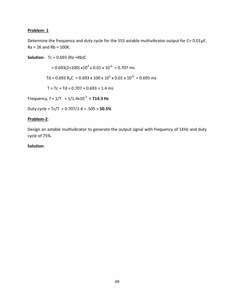
69
Problem- 1
Determine the frequency and duty cycle for the 555 astable multivibrator output for C= 0.01µF,
Ra = 2K and Rb = 100K.
Solution: Tc = 0.693 (Ra +Rb)C
= 0.693(2+100) x103 x 0.01 x 10-6 = 0.707 ms
Td = 0.693 RbC = 0.693 x 100 x 103 x 0.01 x 10-6 = 0.693 ms
T = Tc + Td = 0.707 + 0.693 = 1.4 ms
Frequency, f = 1/T = 1/1.4x10-3 = 714.3 Hz
Duty cycle = Tc/T = 0.707/1.4 = .505 = 50.5%
Problem-2:
Design an astable multivibrator to generate the output signal with frequency of 1KHz and duty
cycle of 75%.
Solution:
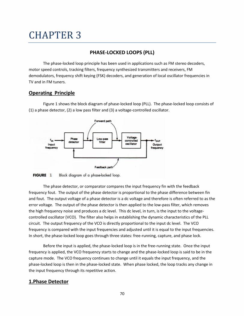
70
CHAPTER 3
PHASE-LOCKED LOOPS (PLL)
The phase-locked loop principle has been used in applications such as FM stereo decoders,
motor speed controls, tracking filters, frequency synthesized transmitters and receivers, FM
demodulators, frequency shift keying (FSK) decoders, and generation of local oscillator frequencies in
TV and in FM tuners.
Operating Principle
Figure 1 shows the block diagram of phase-locked loop (PLL). The phase-locked loop consists of
(1) a phase detector, (2) a low pass filter and (3) a voltage-controlled oscillator.
The phase detector, or comparator compares the input frequency fin with the feedback
frequency fout. The output of the phase detector is proportional to the phase difference between fin
and fout. The output voltage of a phase detector is a dc voltage and therefore is often referred to as the
error voltage. The output of the phase detector is then applied to the low-pass filter, which removes
the high frequency noise and produces a dc level. This dc level, in turn, is the input to the voltage-
controlled oscillator (VCO). The filter also helps in establishing the dynamic characteristics of the PLL
circuit. The output frequency of the VCO is directly proportional to the input dc level. The VCO
frequency is compared with the input frequencies and adjusted until it is equal to the input frequencies.
In short, the phase-locked loop goes through three states: free-running, capture, and phase lock.
Before the input is applied, the phase-locked loop is in the free-running state. Once the input
frequency is applied, the VCO frequency starts to change and the phase-locked loop is said to be in the
capture mode. The VCO frequency continues to change until it equals the input frequency, and the
phase-locked loop is then in the phase-locked state. When phase locked, the loop tracks any change in
the input frequency through its repetitive action.
1.Phase Detector

71
The phase detector compares the input frequency and the VCO frequency and generates a dc
voltage that is proportional to the phase difference between the two frequencies. Depending on
whether the analog or digital phase detector is used, the PLL is called either an analog or digital type,
respectively. Even though most of the monolithic PLL integrated circuits use analog phase detectors, the
majority of discrete phase detectors in use are of the digital type mainly because of its simplicity. For
this reason, we shall consider only digital type phase detectors here.
A double-balanced mixer is a classic example of an analog phase detector. On the other hand,
examples of digital phase detectors are:
1. Exclusive-OR phase detector
2. Edge-triggered phase detector
3. Monolithic phase detector
1. Exclusive-OR phase detector
Figure 2(a) shows the exclusive-OR phase detector that uses an exclusive-OR gate such as CMOS type
4070. The output of the exclusive-OR gate is high only when fin or fout is high, as shown in figure 2(b)
Figure 2(a)

72
Figure 2(b)
In this figure, fin is leading fout by ɸ(phi) degrees; that is, the phase difference between fin and
fout is ɸ degrees. The dc output voltage of the exclusive-OR phase detector is a function of the phase
difference between its two inputs.
Figure 2(c)
Figure 2(c) shows dc output voltage as a function of the phase difference between fin and fout.
This graph indicates that the maximum dc output voltage occurs when the phase difference is π radians
or 180°. The slope of the curve between 0 and π radians is the conversion gain kp of the phase detector.
For example, if the exclusive-OR gate uses a supply voltage Vcc = 5V, the conversion gain kp is
Kp =
= 1.59V/rad
The exclusive-OR type of phase detector is generally used if the fin and fout are square waves.
The edge-triggered phase detector, on the other hand, is preferred if the fin and fout are pulse
waveforms with less than 50% duty cycles.
2. Edge-triggered phase detector
Figure 3(a) shows the edge-triggered type of phase detector using an R-S ( reset-set) flip-flop.
The R-S flip-flop, in turn, is formed from a pair of cross coupled NOR gates. The R-S flip-flop is triggered;
that is the output of the detector changes its logic state on the positive (leading) edge of the inputs fin
and fout [Figure 3(b)]. The graph of the dc output voltage versus phase difference between fin and fout
is shown in Figure 3(c).
The advantages of the edge-triggered phase detector over the exclusive-OR type of detector are
(1) the dc output voltage is linear over 2π radians or 360°, as opposed to π radians or 180° in the case of
the exclusive-OR detector, and
(2) the edge-triggered detector also exhibits better capture, tracking, and locking characteristics than
the exclusive-OR detector.

73
However, both types of detectors are sensitive to harmonics of the input signal and changes in the duty
cycles of fin and fout.
Figure 3(a)
Figure 3(b)
Figure 3(c)
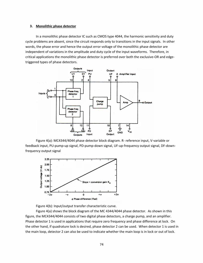
74
3. Monolithic phase detector
In a monolithic phase detector IC such as CMOS type 4044, the harmonic sensitivity and duty
cycle problems are absent, since the circuit responds only to transitions in the input signals. In other
words, the phase error and hence the output error voltage of the monolithic phase detector are
independent of variations in the amplitude and duty cycle of the input waveforms. Therefore, in
critical applications the monolithic phase detector is preferred over both the exclusive-OR and edge-
triggered types of phase detectors.
Figure 4(a): MC4344/4044 phase detector block diagram. R- reference input, V-variable or
feedback input, PU-pump-up signal, PD-pump-down signal, UF-up-frequency output signal, DF-down-
frequency output signal
Figure 4(b): Input/output transfer characteristic curve.
Figure 4(a) shows the block diagram of the MC 4344/4044 phase detector. As shown in this
figure, the MC4344/4044 consists of two digital phase detectors, a charge pump, and an amplifier.
Phase detector 1 is used in applications that require zero frequency and phase difference at lock. On
the other hand, if quadrature lock is desired, phase detector 2 can be used. When detector 1 is used in
the main loop, detector 2 can also be used to indicate whether the main loop is in lock or out of lock.

75
The input/output transfer characteristic curve of phase detector 1 is shown in Fig. 4(b). As
shown here, the curve is linear over 4π radians or 720° and has a conversion gain kp of 1.5V/4π =
0.12V/rad.
2.Low- Pass filter
The function of the low pass filter is to remove the high frequency components in the output of
the phase detector and to remove high frequency noise. The low-pass filter controls the dynamic
characteristics of the phase-locked loop. These characteristics include capture and lock ranges, band
width, and transient response.
Lock range
The lock range is defined as the range of frequencies over which the PLL system follows the
changes in the input frequency fin. An equivalent term for lock range is tracking range. The lock range
is usually expressed as percentage of the VCO frequency.
Capture range
The range of frequencies over which the PLL can acquire lock with an input signal is called the
capture range. The capture range is always smaller than the lock range. This is expressed as percentage
of fo.
Pull-in time
The total time taken by the PLL to establish lock is called pull-in time. This depends on the initial
phase and frequency difference between two signals as well as on the overall loop gain and loop filter
characteristics.
As the filter bandwidth is reduced, its response time increases. However, reduced bandwidth
reduces the capture range of the PLL. Nevertheless, reduced bandwidth helps to keep the loop in lock
through momentary losses of signal and also minimizes noise.
The loop filter used in the PLL may be one of the three types shown in Figure 5. With the
passive filters of Figure 5(a) and (b), an amplifier is generally used for gain. On the other hand, the
active filter of Figure 5(c) includes the gain.

76
Figure 5(a) (b) Passive filter
Figure 5(c) Active filter
3.Voltage-Controlled Oscillator
The third section of the PLL is the voltage-controlled oscillator. The VCO generates an output
frequency that is directly proportional to its input voltage. The block diagram of the VCO is shown in
Figure 6(a).
Figure 6(a) VCO block diagram
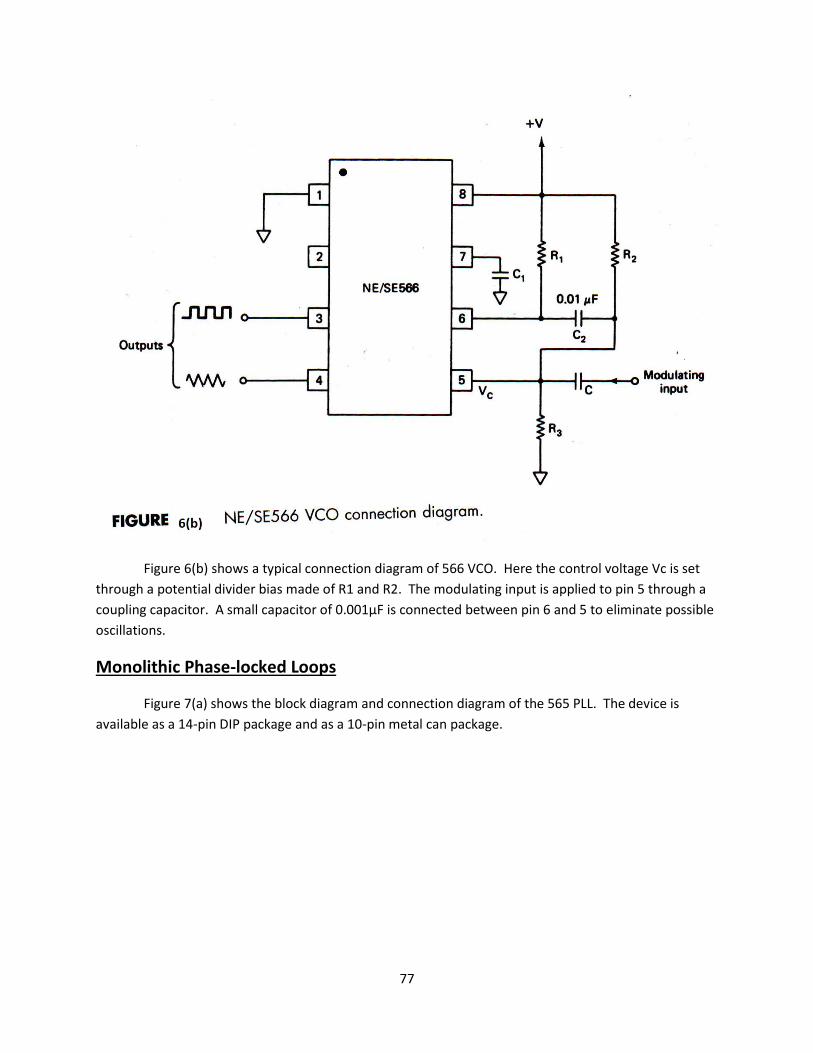
77
Figure 6(b) shows a typical connection diagram of 566 VCO. Here the control voltage Vc is set
through a potential divider bias made of R1 and R2. The modulating input is applied to pin 5 through a
coupling capacitor. A small capacitor of 0.001µF is connected between pin 6 and 5 to eliminate possible
oscillations.
Monolithic Phase-locked Loops
Figure 7(a) shows the block diagram and connection diagram of the 565 PLL. The device is
available as a 14-pin DIP package and as a 10-pin metal can package.
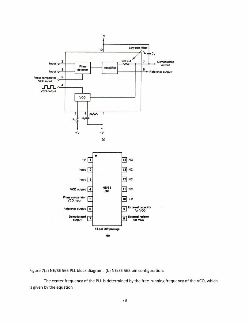
78
Figure 7(a) NE/SE 565 PLL block diagram. (b) NE/SE 565 pin configuration.
The center frequency of the PLL is determined by the free-running frequency of the VCO, which
is given by the equation
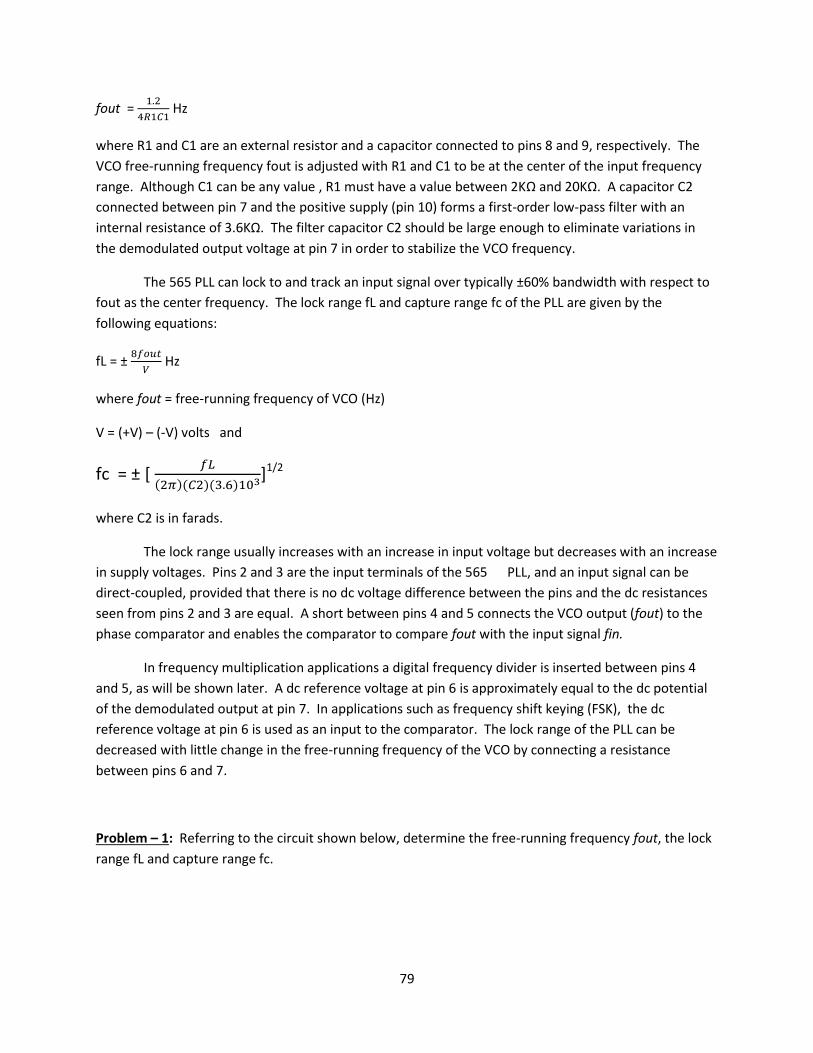
79
fout =
Hz
where R1 and C1 are an external resistor and a capacitor connected to pins 8 and 9, respectively. The
VCO free-running frequency fout is adjusted with R1 and C1 to be at the center of the input frequency
range. Although C1 can be any value , R1 must have a value between 2KΩ and 20KΩ. A capacitor C2
connected between pin 7 and the positive supply (pin 10) forms a first-order low-pass filter with an
internal resistance of 3.6KΩ. The filter capacitor C2 should be large enough to eliminate variations in
the demodulated output voltage at pin 7 in order to stabilize the VCO frequency.
The 565 PLL can lock to and track an input signal over typically ±60% bandwidth with respect to
fout as the center frequency. The lock range fL and capture range fc of the PLL are given by the
following equations:
fL = ±
Hz
where fout = free-running frequency of VCO (Hz)
V = (+V) – (-V) volts and
fc = ± [
]1/2
where C2 is in farads.
The lock range usually increases with an increase in input voltage but decreases with an increase
in supply voltages. Pins 2 and 3 are the input terminals of the 565 PLL, and an input signal can be
direct-coupled, provided that there is no dc voltage difference between the pins and the dc resistances
seen from pins 2 and 3 are equal. A short between pins 4 and 5 connects the VCO output (fout) to the
phase comparator and enables the comparator to compare fout with the input signal fin.
In frequency multiplication applications a digital frequency divider is inserted between pins 4
and 5, as will be shown later. A dc reference voltage at pin 6 is approximately equal to the dc potential
of the demodulated output at pin 7. In applications such as frequency shift keying (FSK), the dc
reference voltage at pin 6 is used as an input to the comparator. The lock range of the PLL can be
decreased with little change in the free-running frequency of the VCO by connecting a resistance
between pins 6 and 7.
Problem – 1: Referring to the circuit shown below, determine the free-running frequency fout, the lock
range fL and capture range fc.
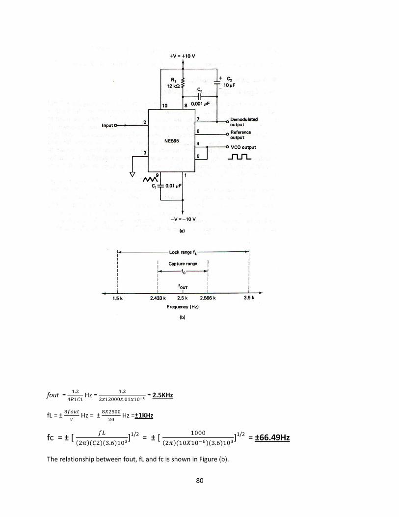
80
fout =
Hz =
= 2.5KHz
fL = ±
Hz = ±
Hz =±1KHz
fc = ± [
]1/2 = ± [
]1/2 = ±66.49Hz
The relationship between fout, fL and fc is shown in Figure (b).
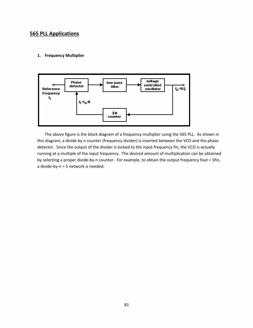
81
565 PLL Applications
1. Frequency Multiplier
The above figure is the block diagram of a frequency multiplier using the 565 PLL. As shown in
this diagram, a divide by n counter (frequency divider) is inserted between the VCO and the phase
detector. Since the output of the divider is locked to the input frequency fin, the VCO is actually
running at a multiple of the input frequency. The desired amount of multiplication can be obtained
by selecting a proper divide-by-n counter. For example, to obtain the output frequency fout = 5fin,
a divide-by-n = 5 network is needed.