linearized cmos high effeciency class-e rf … · linearized cmos high effeciency class-e rf power...
TRANSCRIPT

LINEARIZED CMOS HIGH EFFECIENCY CLASS-E RF POWER AMPLIFIER
SAAD M. AL-SHAHARANI Department of Electrical Engineering
King Fahd University of Petroleum and Minerals Box 185, Dhahran 31261, SAUDI ARABIA
http://faculty.kfupm.edu.sa/ee/saadms/ Abstract: - This paper presents a CMOS class-E power amplifier that has a simple structure and exhibits high linearity. The amplifier operates at 900 MHz from a 2.5-V, and delivers 1-W output power with 80% drain efficiency. Simulation results show that 3rd and 5th IMD products of the proposed PA are lower than that of the conventional class-E amplifier by 14 dB and 9dB respectively. The proposed amplifier shows a good performance when tested with linear modulation scheme such as that used in North American Digital Cellular (NADC). Key-Words: CMOS, Class-E, RF, Power Amplifier. 1 Introduction Last few years have seen an increase in the popularity of the wireless communication systems. As a result, the demand for compact, low-cost, and low power portable transceivers has increased dramatically [1]. A proposed solution is single-chip radio transceiver realized in a low-cost CMOS, [2][3]. Since it is known that Radio Frequency (RF) power amplifier (PA) consumes most of the dissipated power within a transmitter, reducing its power consumption will improve the transceiver performance. Due to its superior performance over the MOS transistors, Gallium Arsenide (GaAs) transistors have been used extensively to build high performance RF PA. GaAs based PAs have several drawbacks: costly to implement, require high level power supply, and have large size. On the other hand, CMOS power amplifier’s has a limited performance because of its low breakdown voltage, low current drive, and lossy substrate. In spite of its limitation, sub-micron CMOS prove to be a good candidate process for RF PA implementation. Recently, several RF power amplifiers have been implemented in a low-cost digital CMOS technology [4-9]. These PAs were designed for constant envelop modulation scheme which are employed by various systems such as European standard for mobile communications and Advanced mobile phone
system (AMPS). The reported amplifiers utilized switching classes amplifiers to achieve their high efficiency and output power. Designing a high efficiency PA for a linearly
modulated RF signal such as that used in NADC is not an easy task. Traditionally, class A or AB amplifiers, which are backed off the compression point, are used in these systems. As a result, these PAs have low efficiency and low output power. Another approach is using high efficiency switching amplifiers with an additional linearization circuit [10-11]. This technique resulted in an amplifier that has good linearity, efficiency, and output power. However, the required linearization circuits usually tend to be very complex and chip’s area and power consuming.
RL
VDD
+ Vi
-
LOCO
CP
LChoke
Figure.1 Single-ended Power Class-E Amplifier
M1
Proceedings of the 5th WSEAS Int. Conf. on Electronics, Hardware, Wireless and Optical Communications, Madrid, Spain, February 15-17, 2006 (pp209-213)

The goal of this work is to design a simple linear CMOS RF PA, which can be used in NADC system. This amplifier is designed to achieve good performance in terms of linearity, efficiency, and output power. Moreover, it does not require additional linearization circuit.
2 Class-E Amplifier The conventional configuration of class-E is a single-transistor amplifier as shown in Fig. 1. Transistor M1 operates as a switch; M1 is on half cycle and off in the other half. A heavily overdriven transistor realizes switching behavior required for class-E operation. Moreover, an adequate load needs to be placed across the realized switch. The analysis of the class-E amplifiers has been reported in several papers [12-16]. Equation (1), which describes the required ZL at the fundamental frequency, is obtained from [14]. Load at second and third harmonics need to be strong reactive load.
oj
ssL e
CZ 4928.0
⋅⋅
=ω
(1)
The resonance frequency of the load is designed to be slightly higher than the fundamental frequency for two reasons: To force the fundamental current only to pass to the load and to provide the transistor with the required inductive load. In [12] and [13] the maximum class-E frequency operation (fmax) for a given device can be respectively approximated as follows:
DDT VCI
f⋅⋅
=5.56
maxmax (2) (high choke inductor
assumption [12])
Tchook Cf
L⋅
= 2max).2(7436.0
π (3) (finite choke inductor
assumption [13]) Imax is the maximum current that the device can provide. CT is the total capacitance across the transistor, which includes intrinsic capacitance, package effects and added capacitance if needed. Usually at radio frequency (RF) the intrinsic capacitance is adequate if not more than sufficient in some cases. Therefore, CT puts a limit on the maximum operating frequency. As depicted in equation (3), fmax can be enhanced by using smaller choke inductor.
As mentioned in [17], the resonance frequency of the output loop has different values when M1 is on and when it is off. This generates harmonic distortion. Steve and Toumazou proposed a new configuration for class-E, Fig. 2 [17]. Based on which transistor is on and which is off, this typology has the following resonance frequencies:
)/()(/1
/1
222222
111
TT CCCCLw
CLw
+⋅=
⋅= (M1 on and M2 off)
)/()(/1
/1
111114
223
TT CCCCLw
CLw
+⋅=
⋅= (M1 off and M2 on)
Harmonic distortion can be minimized by making w1 and w3 equal to the operating frequency wo. Although this configuration can provide two equal resonance frequencies in both cycles, it generates other distortion frequencies, w2 and w4. Another disadvantage of Fig. 2, it uses a PMOS transistor. It is known that PMOS transistors have lower transconductance gain and operating frequency compared to the NMOS transistors.
3 Proposed Typology Figure 3 shows the proposed class-E output stage. Ideally, M1 and M2 act as switches; one-transistor switches on and the other off alternatively every half cycle. This typology uses NMOS transistors only. V1 and V2 have equal amplitude and are 180 degrees out off phase. By proper selection of Cp1 and Cp2, the resonance frequency will be the same in both half cycles, )/()((/1 ToToooo CCCCCLw +⋅+= . In fact, due to the non-ideality of the switches there will be still harmonic distortion. This circuit is expected to generate less harmonics distortion compare to the other circuits. Advantages of the proposed circuit: • It uses the differential structure which results in
lower drain peak voltage required to deliver certain output power compared to the conventional class-E. This point was proved by simulation; two 1-watt PA circuits were implemented one uses the conventional typology and the other uses the proposed one. The conventional and the proposed circuits have a peak voltage of 8V and 6.4V respectively.
Proceedings of the 5th WSEAS Int. Conf. on Electronics, Hardware, Wireless and Optical Communications, Madrid, Spain, February 15-17, 2006 (pp209-213)
50Ω
VDD
+ V1
4pF
VDD
+ V2
18pF
18pF
4pF
3.3n
3nH
3nH
15p
3.5n
15p
7nH
12pF
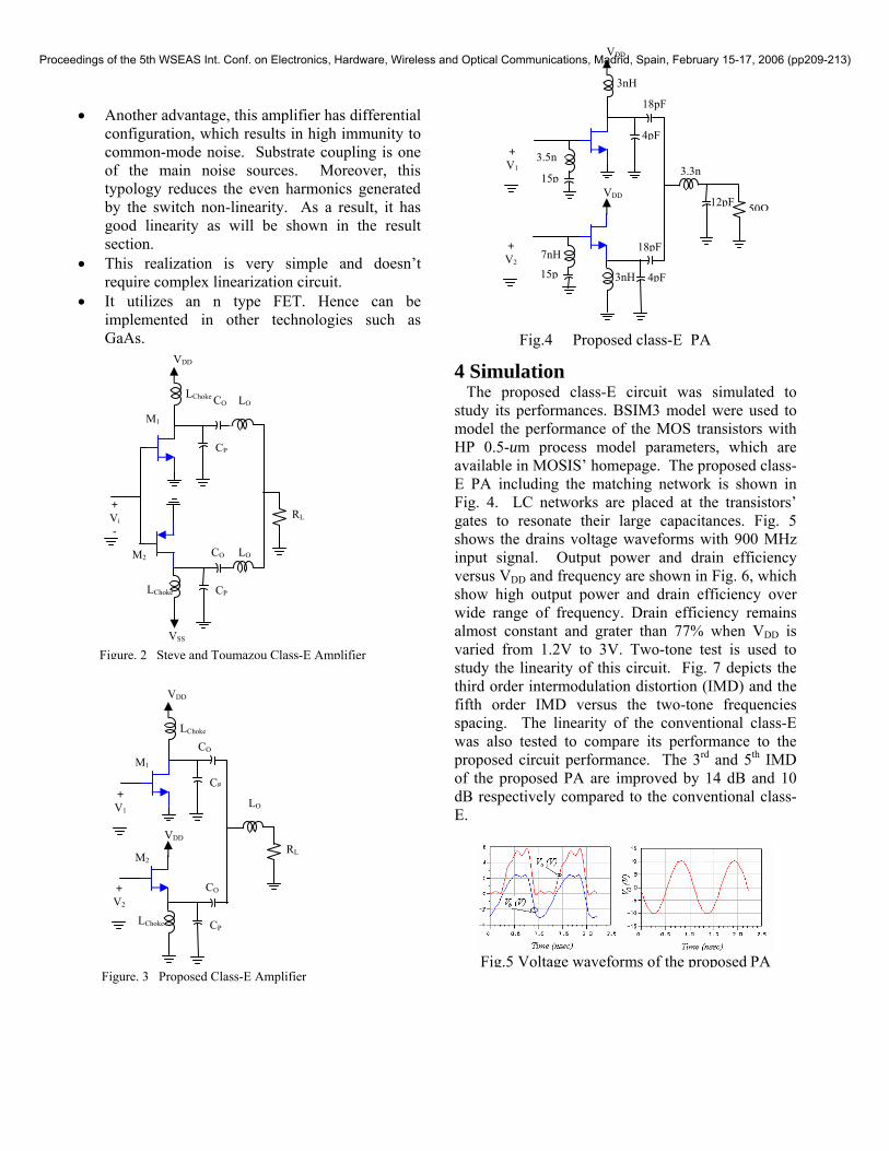
Fig.4 Proposed class-E PA
• Another advantage, this amplifier has differential configuration, which results in high immunity to common-mode noise. Substrate coupling is one of the main noise sources. Moreover, this typology reduces the even harmonics generated by the switch non-linearity. As a result, it has good linearity as will be shown in the result section.
• This realization is very simple and doesn’t require complex linearization circuit.
• It utilizes an n type FET. Hence can be implemented in other technologies such as GaAs.
ws the drains voltage waveforms with 900 MHz input signal. Output power and drain efficiency versus VDD and frequency are shown in Fig. 6, which show high output power and drain efficiency over wide range of frequency. Drain efficiency remains almost constant and grater than 77% when VDD is varied from 1.2V to 3V. Two-tone test is used to study the linearity of this circuit. Fig. 7 depicts the thir the
fth order IMD versus the two-tone frequencies acing. The linearity of the conventional class-E as also tested to compare its performance to the
4 Simulation The proposed class-E circuit was simulated to study its performances. BSIM3 model were used to model the performance of the MOS transistors with HP 0.5-um process model parameters, which are available in MOSIS’ homepage. The proposed class-E PA including the matching network is shown in Fig. 4. LC networks are placed at the transistors’ gates to resonate their large capacitances. Fig. 5 sho
d order intermodulation distortion (IMD) and fispwproposed circuit performance. The 3rd and 5th IMD of the proposed PA are improved by 14 dB and 10 dB respectively compared to the conventional class-E.
RL
VDD
+ V1
LO
CO
CP
L okeCh
VDD
CO
LChoke CP
+ V2
Figure. 3 Proposed Class-E Amplifier
M1
M2
RL
VDD
+ Vi -
LOCO
CP
LChoke
VSS
LOCO
LChoke CP
M1
M2
Figure. 2 Steve and Toumazou Class-E Amplifier
Fig.5 Voltage waveforms of the proposed PA
Proceedings of the 5th WSEAS Int. Conf. on Electronics, Hardware, Wireless and Optical Communications, Madrid, Spain, February 15-17, 2006 (pp209-213)
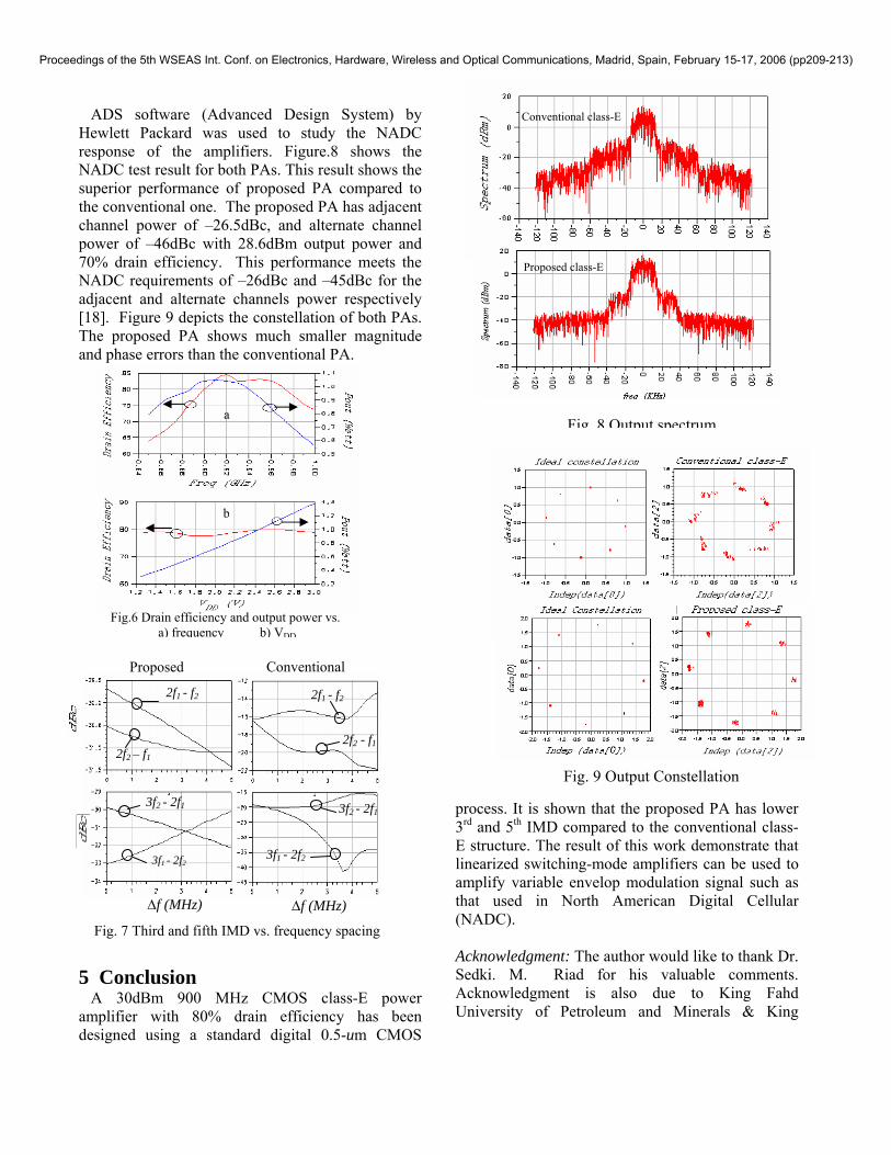
ADS software (Advanced Design System) by Hewlett Packard was used to study the NADC response of the amplifiers. Figure.8 shows the NADC test result for both PAs. This result shows the superior performance of proposed PA compared to the conventional one. The proposed PA has adjacent channel power of –26.5dBc, and alternate channel power of –46dBc with 28.6dBm output power and 70% drain efficiency. This performance meets the NADC requirements of –26dBc and –45dBc for the adjacent and alternate channels power respectively [18]. Figure 9 depicts the constellation of both PAs. The proposed PA shows much smaller magnitude and phase errors than the conventional PA.
drain efficiency has been designed using a standard digital 0.5-um CMOS
5 Conclusion A 30dBm 900 MHz CMOS class-E power amplifier with 80%
process. It is shown that the proposed PA has lower 3rd and 5th IMD compared to the conventional class-E structure. The result of this work demonstrate that linearized switching-mode amplifiers can be used to amplify variable envelop modulation signal such as that used in North American Digital Cellular (NADC). Acknowledgment: The author would like to thank Dr. Sedki. M. Riad for his valuable comments. Acknowledgment is also due to King Fahd University of Petroleum and Minerals & King
Fig.6 Drain efficiency and output power vs. a) frequency b) VDD
b
a
Fig. 9 Output Constellation
2f1 - f2
2f2 - f1 2f
3f2 - 2f1
3f1 - 2f2
3f
2 – f1
2f1 - f2
2 - 2f1
3f1 - 2f2
∆f (MHz) ∆f (MHz)
Proposed Conventional
Fig. 7 Third
Fig 8 Output spectrum
Conventional class-E
Proposed class-E
and fifth IMD vs. frequency spacing
Proceedings of the 5th WSEAS Int. Conf. on Electronics, Hardware, Wireless and Optical Communications, Madrid, Spain, February 15-17, 2006 (pp209-213)

Abdulaziz City for Science and Technology for supporting the work. References [1] P. Gray and R. Meyer, “Future Directions of Silicon IC’s for RF Personal Communications,” IEEE Custom Integrated Circuits Conference. Dig, pp. 90-93, May, 1995. [2] A. Rofougaran, G. Chang, J. Rael, M.
IEEE Journal of Solid-State Circuits, vol.
ta, C. Nilson, L. Plouvier, and S.
s, vol. 34, no. 7, pp. 962-970, 1999.
.8 p.445-449, August, 2003.
[9] A. Shirvani, D. Su, and B. Wooley, “A CMOS RF Power Amplifier With Parallel Amplification for Efficient Power Control,” IEEE Journal Solid-State Circuits, vol. 37 no. 6, pp. 648 –693, June. 2002. [10] T. Sowlati, Y. Greshishchev, C. Salama, G. Rabjohn,and J. Sitch , “ Linearized High Efficiency Class E Power Amplifier for Wireless Communications,” IEEE Custom Integrated Circuits Conference. Dig, pp. 201-204, 1996.
[11] D. Su and W. MacFarland, “An IC for Linearizing RF Power Amplifiers Using Envelope Elimination and Restoration,” IEEE Journal Solid-State Circuits, vol. 33 no. 12, pp. 2252 –2258, Dec. 1998. [12] T. Mader, “ Quasi-Optical Class-E Power Amplifiers,” Ph.D. dissertation, University of Colorado, 1995. [13] C.-H. Li and Y.-O.Yam, “Maximum frequency and optimum performance of class E power amplifiers,” IEE Proceedings- Circuits, Devices and Systems, vol. 141, no. 3, pp. 174 –184, June, 1994. [14] N. Sokal and A. Sokal, “ Class-E, a new class of high efficiency tuned single-ended switching power amplifiers,” IEEE Journal of Solid State Circuits, vol. SC-20, no. 3, pp. 168-176, June, 1975. [15] M. Kazimierczuk, “ Effects of the collector current fall time on class E tuned power amplifier,” IEEE Journal of Solid State Circuits, vol. SC-18, pp. 181-193, April, 1983. [16] F. Raab, “ Idealized Operation of the Class E Tuned Amplifier,” IEEE Transactions on Circuits and Systems, vol. CAS-24, no.2 pp.239-247, April, 1978. [17] S. Tu and C. Toumazou, “Design of low-distortion CMOS Class E Power Amplifier for Wireless Communications,” IEEE International Symposium on Circuits and Systems, Dig, pp. 1433-1436, 1999. [18] J. Kenney and A. Leke, “Power amplifier spectral regrowth for digital cellular and PCS applications,” Microwave J., pp. 74-92, Oct. 1995.
Rofougaran, S. Khorram, M-K. Ku, E. Roth, A. Abidi, and H. Samueli, “A single-chip 900-MHz Spread-Spectrum wireless transceiver in 1-mm CMO-Part1: Architecture and transmitter design,”33, pp. 513-534, Apr. 1998. [3] T. Cho, E. Dukatz, M. Mack, D. MacNally, M. Marring, S. MehRabii, “ A single-chip CMOS direct-conversion transceiver for 900 MHz spread-spectrum digital cordless phones,” ISSCC Dig. Tech. Papers, San Francisco, CA, Feb. 1999. [4] M. Rofougaran, A. Rofougaran, C. Olgaard, and A. Abidi “A 900 MHz CMOS RF Power Amplifier with Programmable Output,” VLSI Circuits Symposium, pp. 133-134, 1994. [5] D. Su and W. MacFarland, “A 2.5-V, 1-W Monolithic CMOS RF Power Amplifier,” IEEE Custom Integrated Circuits Conference. Dig, pp. 189-192, 1997. [6] K. Tsai and P. Gray, “A 1.9-GHz, 1-W CMOS Class-E Power Amplifier for Wireless Communications,” IEEE Journal of Solid-State Circuit[7] C. Yoo and Q. Huang, “A Common-Gate Switched, 0.9W Class-E Power Amplifier with 41% PAE in 0.25µm CMOS,” IEEE VLSI Circuits Symposium Digest of Technical Papers, pp. 56-57, 2000. [8] K. HO and H. Luong, “ A 1-V CMOS Power Amplifier for Bluetooth Applications,” IEEE Transactions on Circuits and Systems, vol. 50, nop
Proceedings of the 5th WSEAS Int. Conf. on Electronics, Hardware, Wireless and Optical Communications, Madrid, Spain, February 15-17, 2006 (pp209-213)