lis3dh application note (an3308) - st.com · 4.2.1 data alignment ..... 16 4.2.2 big-little endian...
TRANSCRIPT

June 2017 DocID18198 Rev 3 1/59
www.st.com
AN3308 Application note
LIS3DH: MEMS digital output motion sensor ultra-low-power high-performance 3-axis “nano” accelerometer
Introduction This document describes the low-voltage 3-axis digital output linear MEMS accelerometer provided in an LGA package.
The LIS3DH is an ultra-low-power high-performance 3-axis linear accelerometer belonging to the “nano” family, with a digital I2C/SPI serial interface standard output.
The device features ultra-low-power operational modes that allow advanced power saving and smart sleep-to-wake-up and return-to-sleep functions.
The LIS3DH has dynamic user-selectable full scales of ±2g/±4g/±8g/±16g and is capable of measuring accelerations with output data rates from 1 Hz to 5 kHz.
The device may be configured to generate interrupt signals using an independent inertial wake-up/free-fall event as well as by the position of the device itself. Thresholds and timing of the interrupt generator are programmable by the end user on the fly.
Automatic programmable sleep-to-wakeup and return-to-sleep functions are also available for enhanced power saving.
The LIS3DH has an integrated 32-level first-in first-out (FIFO) buffer allowing the user to store data in order to limit intervention by the host processor.
The LIS3DH is available in a small thin plastic land grid array package (LGA) and is guaranteed to operate over an extended temperature range from -40 °C to +85 °C.
The ultra-small size and weight of the SMD package make it an ideal choice for handheld portable applications such as smartphones, IoT connected devices, and wearables, or any other application where reduced package size and weight are required.

Contents AN3308
2/59 DocID18198 Rev 3
Contents 1 Pin description ................................................................................ 6
2 Registers .......................................................................................... 7
3 Operating modes ............................................................................. 9
3.1 Power-down mode .......................................................................... 10
3.2 Low-power mode ............................................................................. 10
3.3 Normal mode ................................................................................... 11
3.4 High-resolution mode ...................................................................... 11
3.5 Switching modes ............................................................................. 12
4 Startup sequence .......................................................................... 13
4.1 Reading acceleration data .............................................................. 13 4.1.1 Using the status register ................................................................... 13 4.1.2 Using the data-ready (DRDY) signal ................................................ 15 4.1.3 Using the block data update (BDU) feature ..................................... 16
4.2 Understanding acceleration data ..................................................... 16 4.2.1 Data alignment ................................................................................. 16 4.2.2 Big-little endian selection .................................................................. 16 4.2.3 Example of acceleration data ........................................................... 17
4.3 High-pass filter ................................................................................ 17 4.3.1 Filter configuration ............................................................................ 18
5 Interrupt generation ...................................................................... 20
5.1 Interrupt pin configuration ............................................................... 20
6 Inertial interrupt ............................................................................. 22
6.1 Duration .......................................................................................... 22
6.2 Threshold ........................................................................................ 22
6.3 Free-fall and wake-up interrupts ...................................................... 23 6.3.1 Inertial wake-up ................................................................................ 24 6.3.2 HP filter bypassed ............................................................................ 25 6.3.3 Using the HP filter ............................................................................. 25
6.4 Free-fall detection ........................................................................... 26
7 6D/4D orientation detection .......................................................... 28
7.1 6D orientation detection .................................................................. 28
7.2 4D orientation direction ................................................................... 30
8 Click and double-click recognition .............................................. 31
AN3308 Contents
DocID18198 Rev 3 3/59
8.1 Single click ...................................................................................... 31
8.2 Double click ..................................................................................... 32
8.3 Register description ........................................................................ 34 8.3.1 CLICK_CFG (38h) ............................................................................ 34 8.3.2 CLICK_SRC (39h) ............................................................................ 35 8.3.3 CLICK_THS (3Ah) ............................................................................ 35 8.3.4 TIME_LIMIT (3Bh) ............................................................................ 36 8.3.5 TIME_LATENCY (3Ch) .................................................................... 36 8.3.6 TIME WINDOW (3Dh) ...................................................................... 36 8.3.7 CTRL_REG3 [Interrupt CTRL register] (22h) ................................... 37
8.4 Examples ........................................................................................ 37 8.4.1 Playing with TIME_LIMIT.................................................................. 38 8.4.2 Playing with TIME_LATENCY .......................................................... 39 8.4.3 Playing with TIME_WINDOW ........................................................... 40
9 First-in first-out (FIFO) buffer ....................................................... 41
9.1 FIFO description .............................................................................. 41
9.2 FIFO registers ................................................................................. 43 9.2.1 CTRL_REG5 (0x24) ......................................................................... 43 9.2.2 FIFO_CTRL_REG (0x2E)................................................................. 44 9.2.3 FIFO_SRC_REG (0x2F)................................................................... 44
9.3 FIFO modes .................................................................................... 46 9.3.1 Bypass mode .................................................................................... 46 9.3.2 FIFO mode ....................................................................................... 46 9.3.3 Stream mode .................................................................................... 47 9.3.4 Stream-to-FIFO mode ...................................................................... 49
9.4 Watermark....................................................................................... 51
9.5 Retrieving data from FIFO ............................................................... 52
10 Activity / Inactivity recognition ..................................................... 53
11 Auxiliary ADC and temperature sensor ....................................... 55
12 Accelerometer self-test procedure ............................................... 56
13 Revision history ............................................................................ 58

List of tables AN3308
4/59 DocID18198 Rev 3
List of tables Table 1: Internal pin status ......................................................................................................................... 6 Table 2: Registers ....................................................................................................................................... 7 Table 3: Operating mode selection ............................................................................................................. 9 Table 4: Data rate configuration ................................................................................................................. 9 Table 5: Current consumption of operating modes .................................................................................. 10 Table 6: Turn-on time for operating mode transition ................................................................................ 12 Table 7: STATUS_REG ............................................................................................................................ 14 Table 8: STATUS_REG description ......................................................................................................... 14 Table 9: Output data registers content vs. acceleration (FS = ±2 g, high-resolution mode) .................... 17 Table 10: High-pass filter mode configuration .......................................................................................... 18 Table 11: Low-power mode - high-pass filter cutoff frequency [Hz] ......................................................... 18 Table 12: Reference mode LSB value ...................................................................................................... 19 Table 13: CTRL_REG3 register ................................................................................................................ 20 Table 14: CTRL_REG3 description .......................................................................................................... 20 Table 15: CTRL_REG6 register ................................................................................................................ 21 Table 16: CTRL_REG6 description .......................................................................................................... 21 Table 17: Interrupt mode configuration ..................................................................................................... 22 Table 18: Duration LSB value in normal mode ......................................................................................... 22 Table 19: INT1_SRC register in 6D positions ........................................................................................... 30 Table 20: CLICK_CFG register ................................................................................................................. 34 Table 21: CLICK_CFG description ........................................................................................................... 34 Table 22: Truth table ................................................................................................................................. 34 Table 23: CLICK_SRC register ................................................................................................................. 35 Table 24: CLICK_SRC description ........................................................................................................... 35 Table 25: CLICK_THS register ................................................................................................................. 35 Table 26: CLICK_THS description ............................................................................................................ 35 Table 27: TIME_LIMIT register ................................................................................................................. 36 Table 28: TIME_LIMIT register description............................................................................................... 36 Table 29: TIME_LATENCY register .......................................................................................................... 36 Table 30: TIME_LATENCY description .................................................................................................... 36 Table 31: TIME_WINDOW description ..................................................................................................... 36 Table 32: TIME_WINDOW description ..................................................................................................... 36 Table 33: CTRL_REG3 register ................................................................................................................ 37 Table 34: CTRL_REG3 description .......................................................................................................... 37 Table 35: FIFO buffer full representation (32nd sample set stored) ......................................................... 41 Table 36: FIFO overrun representation (33rd sample set stored and 1st sample discarded) .................. 42 Table 37: FIFO enable bit in CTRL_REG5 ............................................................................................... 43 Table 38: FIFO_CTRL_REG .................................................................................................................... 44 Table 39: FIFO_SRC_REG ...................................................................................................................... 44 Table 40: FIFO_SRC_REG behavior assuming FTH[4:0] = 15 ................................................................ 45 Table 41: CTRL_REG3 (0x22) ................................................................................................................. 45 Table 42: Document revision history ........................................................................................................ 58

AN3308 List of figures
DocID18198 Rev 3 5/59
List of figures Figure 1: Pin connections ........................................................................................................................... 6 Figure 2: DRDY signal synchronization .................................................................................................... 15 Figure 3: Data-ready signal ...................................................................................................................... 15 Figure 4: High-pass filter connections block diagram ............................................................................... 17 Figure 5: Reading REFERENCE .............................................................................................................. 18 Figure 6: Reference mode ........................................................................................................................ 19 Figure 7: Autoreset ................................................................................................................................... 19 Figure 8: Free-fall, wake-up interrupt generator ....................................................................................... 23 Figure 9: FF_WU_CFG high and low ....................................................................................................... 24 Figure 10: Inertial wake-up interrupt ......................................................................................................... 24 Figure 11: Free-fall interrupt ..................................................................................................................... 26 Figure 12: ZH, ZL, YH, YL, XH, and XL behavior ..................................................................................... 28 Figure 13: 6D movement vs. 6D position.................................................................................................. 29 Figure 14: 6D recognized positions .......................................................................................................... 29 Figure 15: Single-click event with non-latched interrupt ........................................................................... 31 Figure 16: Single and double-click recognition ......................................................................................... 32 Figure 17: Double-click recognition .......................................................................................................... 33 Figure 18: Short time limit ......................................................................................................................... 38 Figure 19: Long time limit ......................................................................................................................... 38 Figure 20: Short latency ............................................................................................................................ 39 Figure 21: Long latency ............................................................................................................................ 39 Figure 22: Short window ........................................................................................................................... 40 Figure 23: Long window ............................................................................................................................ 40 Figure 24: FIFO_EN connection block diagram ....................................................................................... 43 Figure 25: FIFO mode behavior ................................................................................................................ 47 Figure 26: Stream mode fast reading behavior ........................................................................................ 48 Figure 27: Stream mode slow reading behavior ....................................................................................... 48 Figure 28: Stream mode slow reading zoom ............................................................................................ 49 Figure 29: Stream-to-FIFO mode: interrupt not latched ........................................................................... 50 Figure 30: Stream-to-FIFO mode: interrupt latched ................................................................................. 50 Figure 31: Watermark behavior - FTH[4:0] = 10 ....................................................................................... 51 Figure 32: FIFO reading diagram - FTH[4:0] = 10 .................................................................................... 52 Figure 33: Activity / Inactivity recognition.................................................................................................. 53 Figure 34: Activity / Inactivity duration ...................................................................................................... 54 Figure 35: Self-test procedure .................................................................................................................. 57
Pin description AN3308
6/59 DocID18198 Rev 3
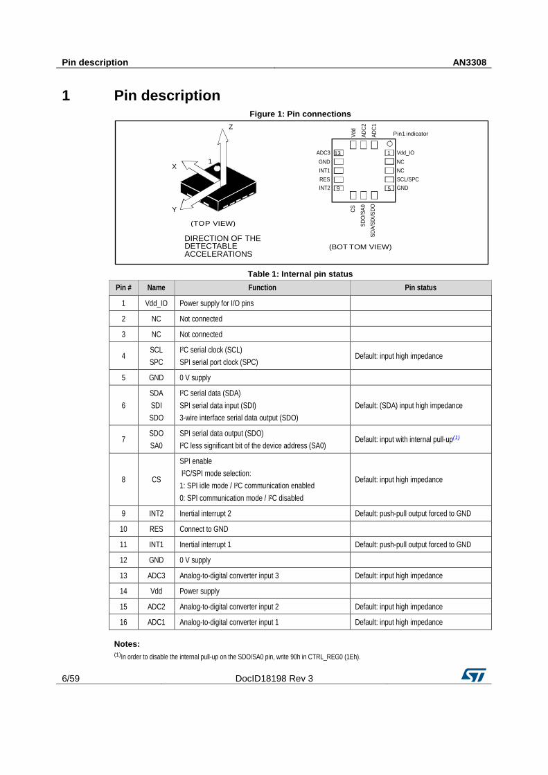
1 Pin description Figure 1: Pin connections
Table 1: Internal pin status
Pin # Name Function Pin status
1 Vdd_IO Power supply for I/O pins 2 NC Not connected 3 NC Not connected
4 SCL SPC
I²C serial clock (SCL) SPI serial port clock (SPC)
Default: input high impedance
5 GND 0 V supply
6 SDA SDI SDO
I²C serial data (SDA) SPI serial data input (SDI) 3-wire interface serial data output (SDO)
Default: (SDA) input high impedance
7 SDO SA0
SPI serial data output (SDO) I²C less significant bit of the device address (SA0)
Default: input with internal pull-up(1)
8 CS
SPI enable I²C/SPI mode selection: 1: SPI idle mode / I²C communication enabled 0: SPI communication mode / I²C disabled
Default: input high impedance
9 INT2 Inertial interrupt 2 Default: push-pull output forced to GND
10 RES Connect to GND 11 INT1 Inertial interrupt 1 Default: push-pull output forced to GND
12 GND 0 V supply 13 ADC3 Analog-to-digital converter input 3 Default: input high impedance
14 Vdd Power supply 15 ADC2 Analog-to-digital converter input 2 Default: input high impedance
16 ADC1 Analog-to-digital converter input 1 Default: input high impedance
Notes: (1)In order to disable the internal pull-up on the SDO/SA0 pin, write 90h in CTRL_REG0 (1Eh).
(TOP VIEW)
DIRECTION OF THEDETECTABLEACCELERATIONS
1
59
13
(BOT TOM VIEW)
Y
1X
ZPin1 indicator
Vdd_IONCNCSCL/SPCGND
SDA/
SDI/S
DOCS
SDO
/SA0
ADC3GNDINT1RESINT2
ADC1
Vdd
ADC2
AN3308 Registers
DocID18198 Rev 3 7/59
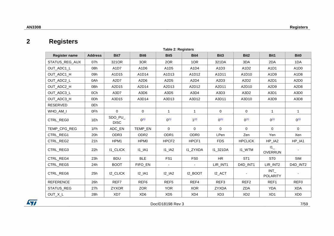
2 Registers Table 2: Registers
Register name Address Bit7 Bit6 Bit5 Bit4 Bit3 Bit2 Bit1 Bit0
STATUS_REG_AUX 07h 321OR 3OR 2OR 1OR 321DA 3DA 2DA 1DA
OUT_ADC1_L 08h A1D7 A1D6 A1D5 A1D4 A1D3 A1D2 A1D1 A1D0
OUT_ADC1_H 09h A1D15 A1D14 A1D13 A1D12 A1D11 A1D10 A1D9 A1D8
OUT_ADC2_L 0Ah A2D7 A2D6 A2D5 A2D4 A2D3 A2D2 A2D1 A2D0
OUT_ADC2_H 0Bh A2D15 A2D14 A2D13 A2D12 A2D11 A2D10 A2D9 A2D8
OUT_ADC3_L 0Ch A3D7 A3D6 A3D5 A3D4 A3D3 A3D2 A3D1 A3D0
OUT_ADC3_H 0Dh A3D15 A3D14 A3D13 A3D12 A3D11 A3D10 A3D9 A3D8
RESERVED 0Eh
WHO_AM_I 0Fh 0 0 1 1 0 0 1 1
CTRL_REG0 1Eh SDO_PU_
DISC 0(1) 0(1) 1(2) 0(1) 0(1) 0(1) 0(1)
TEMP_CFG_REG 1Fh ADC_EN TEMP_EN 0 0 0 0 0 0
CTRL_REG1 20h ODR3 ODR2 ODR1 ODR0 LPen Zen Yen Xen
CTRL_REG2 21h HPM1 HPM0 HPCF2 HPCF1 FDS HPCLICK HP_IA2 HP_IA1
CTRL_REG3 22h I1_CLICK I1_IA1 I1_IA2 I1_ZYXDA I1_321DA I1_WTM I1_
OVERRUN -
CTRL_REG4 23h BDU BLE FS1 FS0 HR ST1 ST0 SIM
CTRL_REG5 24h BOOT FIFO_EN - - LIR_INT1 D4D_INT1 LIR_INT2 D4D_INT2
CTRL_REG6 25h I2_CLICK I2_IA1 I2_IA2 I2_BOOT I2_ACT - INT_
POLARITY -
REFERENCE 26h REF7 REF6 REF5 REF4 REF3 REF2 REF1 REF0
STATUS_REG 27h ZYXOR ZOR YOR XOR ZYXDA ZDA YDA XDA
OUT_X_L 28h XD7 XD6 XD5 XD4 XD3 XD2 XD1 XD0

Registers AN3308
8/59 DocID18198 Rev 3
Register name Address Bit7 Bit6 Bit5 Bit4 Bit3 Bit2 Bit1 Bit0
OUT_X_H 29h XD15 XD14 XD13 XD12 XD11 XD10 XD9 XD8
OUT_Y_L 2Ah YD7 YD6 YD5 YD4 YD3 YD2 YD1 YD0
OUT_Y_H 2Bh YD15 YD14 YD13 YD12 YD11 YD10 YD9 YD8
OUT_Z_L 2Ch ZD7 ZD6 ZD5 ZD4 ZD3 ZD2 ZD1 ZD0
OUT_Z_H 2Dh ZD15 ZD14 ZD13 ZD12 ZD11 ZD10 ZD9 ZD8
FIFO_CTRL_REG 2Eh FM1 FM0 TR FTH4 FTH3 FTH2 FTH1 FTH0
FIFO_SRC_REG 2Fh WTM OVRN_FIFO EMPTY FSS4 FSS3 FSS2 FSS1 FSS0
INT1_CFG 30h AOI 6D ZHIE ZLIE YHIE YLIE XHIE XLIE
INT1_SRC 31h 0 IA ZH ZL YH YL XH XL
INT1_THS 32h 0 THS6 THS5 THS4 THS3 THS2 THS1 THS0
INT1_DURATION 33h 0 D6 D5 D4 D3 D2 D1 D0
INT2_CFG 34h AOI 6D ZHIE ZLIE YHIE YLIE XHIE XLIE
INT2_SRC 35h 0 IA ZH ZL YH YL XH XL
INT2_THS 36h 0 THS6 THS5 THS4 THS3 THS2 THS1 THS0
INT2_DURATION 37h 0 D6 D5 D4 D3 D2 D1 D0
CLICK_CFG 38h - - ZD ZS YD YS XD XS
CLICK_SRC 39h - IA DCLICK SCLICK Sign Z Y X
CLICK_THS 3Ah LIR_CLICK Ths6 Ths5 Ths4 Ths3 Ths2 Ths1 Ths0
TIME_LIMIT 3Bh - TLI6 TLI5 TLI4 TLI3 TLI2 TLI1 TLI0
TIME_LATENCY 3Ch TLA7 TLA6 TLA5 TLA4 TLA3 TLA2 TLA1 TLA0
TIME_WINDOW 3Dh TW7 TW6 TW5 TW4 TW3 TW2 TW1 TW0
ACT_THS 3Eh - Acth6 Acth5 Acth4 Acth3 Acth2 Acth1 Acth0
INACT_DUR 3Fh ActD7 ActD6 ActD5 ActD4 ActD3 ActD2 ActD1 ActD0
Notes: (1)This bit must be set to 0 for correct operation of the device. (2)This bit must be set to 1 for correct operation of the device.

AN3308 Operating modes
DocID18198 Rev 3 9/59
3 Operating modes The LIS3DH provides four different operating modes: power-down mode, high-resolution/normal mode, and low-power mode. While normal mode guarantees higher resolution, low-power mode further reduces the current consumption.
After the power supply is applied, the LIS3DH performs a 5 ms boot procedure to load the trimming parameter. After the boot is completed, the device is automatically configured in power-down mode.
Referring to the LIS3DH datasheet, the output data rate (ODR) and the low-power enable (LPen) bits of CTRL_REG1 and the HR bits of CTRL_REG4 are used to select the operating modes (power-down mode, high-resolution/normal mode and low-power mode) and output data rate (Table 3: "Operating mode selection" and Table 4: "Data rate configuration").
Table 3: Operating mode selection
Operating mode CTRL_REG1[3]
(LPen bit) CTRL_REG4[3]
(HR bit) BW [Hz]
Turn-on time [ms]
So @ ±2g [mg/digit]
Low-power mode (8-bit data output)
1 0 ODR/2 1 16
Normal mode (10-bit data output)
0 0 ODR/2 1.6 4
High-resolution mode (12-bit data output)
0 1 ODR/9 7/ODR 1
Not allowed 1 1 -- -- --
Table 4: Data rate configuration ODR3 ODR2 ODR1 ODR0 Power mode selection
0 0 0 0 Power-down mode
0 0 0 1 HR/Normal /Low-power mode (1 Hz)
0 0 1 0 HR/Normal/Low-power mode (10 Hz)
0 0 1 1 HR/Normal/Low-power mode (25 Hz)
0 1 0 0 HR/Normal/Low-power mode (50 Hz)
0 1 0 1 HR/Normal/Low-power mode (100 Hz)
0 1 1 0 HR/Normal/Low-power mode (200 Hz)
0 1 1 1 HR/Normal/Low-power mode (400 Hz)
1 0 0 0 Low-power mode (1.60 kHz)
1 0 0 1 Normal (1.344 kHz)/Low-power mode (5.376 kHz)

Operating modes AN3308
10/59 DocID18198 Rev 3
Table 5: "Current consumption of operating modes" shows the typical values of the power consumption for the different operating modes.
Table 5: Current consumption of operating modes
Operating mode [Hz] Low-power mode (8-bit data output)
[µA]
Normal mode (10-bit data output)
[µA]
High resolution (12-bit data output)
[µA]
1 2 2 2
10 3 4 4
25 4 6 6
50 6 11 11
100 10 20 20
200 18 38 38
400 36 73 73
1344 -- 185 185
1620 100 -- --
5376 185 -- --
3.1 Power-down mode When the device is in power-down mode, almost all internal blocks of the device are switched off to minimize power consumption. Digital interfaces (I2C and SPI) are still active to allow communication with the device. The content of the configuration registers is preserved and output data registers are not updated, therefore keeping the last data sampled in memory before going into power-down mode.
3.2 Low-power mode In low-power mode, data are generated at the data rate selected through the ODR bits and for the axis enabled through the Zen, Yen, and Xen bits of CTRL_REG1. Data generated for a disabled axis is 00h.
In low-power mode the acceleration data resolution is 8-bit, left-aligned and is stored in the OUT registers (from 28h to 2D).
In order to enable low-power mode, clear the HR bit in CTRL_REG4 and set the LPen bit in CTRL_REG1.
Data interrupt generation is active and configured through INT1_CFG and INT2_CFG and can be routed to the INT1 or INT2 pin through the CTRL_REG3 and CTRL_REG6 registers.

AN3308 Operating modes
DocID18198 Rev 3 11/59
3.3 Normal mode In Normal mode, data are generated at the data rate selected through the ODR bits and for the axis enabled through the Zen, Yen, and Xen bits of CTRL_REG1. Data generated for a disabled axis is 00h.
In Normal mode the acceleration data resolution is 10-bit, left-aligned and is stored in the OUT registers (from 28h to 2D).
In order to enable Normal Mode, clear the HR bit in CTRL_REG4 and clear the LPen bit in CTRL_REG1.
Data interrupt generation is active and configured through INT1_CFG and INT2_CFG and can be routed to the INT1 or INT2 pin through the CTRL_REG3 and CTRL_REG6 registers.
3.4 High-resolution mode In high-resolution mode, data are generated at the data rate selected through the ODR bits and for the axis enabled through the Zen, Yen, and Xen bits of CTRL_REG1. Data generated for a disabled axis is 00h.
In high-resolution mode the acceleration data resolution is 12-bit, left-aligned and is stored in OUT registers (from 28h to 2D).
In order to enable high-resolution mode, set the HR bit in CTRL_REG4 and clear the LPen bit in CTRL_REG1.
Data interrupt generation is active and configured through INT1_CFG and INT2_CFG and can be routed to the INT1 or INT2 pin through the CTRL_REG3 and CTRL_REG6 registers.
It is recommended to read register REFERENCE (26h) when the device operating mode is switched from high-resolution configuration (HR) to power-down mode (PD); this operation resets the filtering block before switching to normal/high-performance mode again:
1. Write 08h into CTRL_REG4 // Set HR
2. Write 57h into CTRL_REG2 // Clear LPen // Enable all axes // ODR = 100 Hz
3. Wait the duration of the turn-on time
4. Write 07h into CTRL_REG2 // Clear LPen // Enable all axes // Power down
5. Read REFERENCE // Reset filter block
6. Write 57h into CTRL_REG2 // Clear LPen // Enable all axes // ODR = 100 Hz
7. Wait the duration of the turn-on time

Operating modes AN3308
12/59 DocID18198 Rev 3
3.5 Switching modes The turn-on time to transition to another operating mode is given in Table 6: "Turn-on time for operating mode transition".
Table 6: Turn-on time for operating mode transition
Operating mode change Turn-on time
[ms]
12-bit mode to 8-bit mode 1/ODR
12-bit mode to 10-bit mode 1/ODR
10-bit mode to 8-bit mode 1/ODR
10-bit mode to 12-bit mode 7/ODR
8-bit mode to 10-bit mode 1/ODR
8-bit mode to 12-bit mode 7/ODR

AN3308 Startup sequence
DocID18198 Rev 3 13/59
4 Startup sequence Once the device is powered up, it automatically downloads the calibration coefficients from the embedded flash to the internal registers. When the boot procedure is completed, i.e. after approximately 5 milliseconds, the device automatically enters power-down mode. To turn on the device and gather acceleration data, select the HR bit in CTRL_REG4 and the LPen bit in CTRL_REG1, enable at least one of the axes and select the preferred ODR.
The following general-purpose sequence can be used to configure the device:
1. Write CTRL_REG1 2. Write CTRL_REG2 3. Write CTRL_REG3 4. Write CTRL_REG4 5. Write CTRL_REG5 6. Write CTRL_REG6 7. Write REFERENCE 8. Write INTx_THS 9. Write INTx_DUR 10. Write INTx_CFG 11. Write CTRL_REG5
4.1 Reading acceleration data 4.1.1 Using the status register
The LIS3DH generates data serially (X first, Y second, Z third). Every time the single-axis data is generated, the corresponding DA signal (XDA, YDA, ZDA) bit of STATUS_REG is set to 1. XDA, YDA, ZDA are individually reset to 0 when the respective higher part of the data is read (ie. XDA goes to 0 as soon as the X-axis higher part of the data (reg. 29h) is read, and so on).
The ZYXDA signal can be set only after Z data generation and is set if XDA, YDA and ZDA bits are simultaneously '1', otherwise the ZYXDA bit is reset to '0' when XDA, YDA and ZDA are simultaneously '0'.
The overrun flags XOR, YOR, ZOR bits are individually set to '1' when the corresponding data is generated and the corresponding DA bit is already at 1, while they are reset to '0' (with corresponding DA bit) when the corresponding data is read.
The ZYXOR bit is set to 1 when at least one overrun flag ( XOR, YOR, ZOR) goes to 1, while the ZYXOR bit is reset to 0 when all the overrun flags are zero.
Startup sequence AN3308
14/59 DocID18198 Rev 3
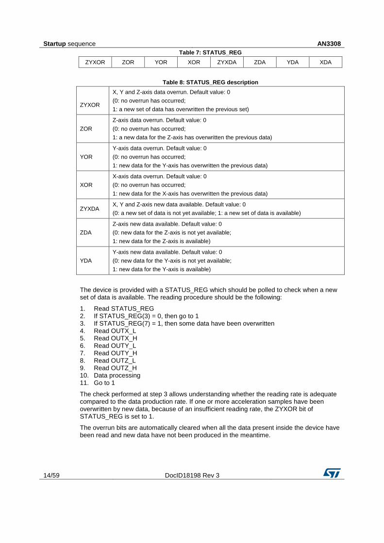
Table 7: STATUS_REG ZYXOR ZOR YOR XOR ZYXDA ZDA YDA XDA
Table 8: STATUS_REG description
ZYXOR
X, Y and Z-axis data overrun. Default value: 0 (0: no overrun has occurred; 1: a new set of data has overwritten the previous set)
ZOR Z-axis data overrun. Default value: 0 (0: no overrun has occurred; 1: a new data for the Z-axis has overwritten the previous data)
YOR Y-axis data overrun. Default value: 0 (0: no overrun has occurred; 1: new data for the Y-axis has overwritten the previous data)
XOR X-axis data overrun. Default value: 0 (0: no overrun has occurred; 1: new data for the X-axis has overwritten the previous data)
ZYXDA X, Y and Z-axis new data available. Default value: 0 (0: a new set of data is not yet available; 1: a new set of data is available)
ZDA Z-axis new data available. Default value: 0 (0: new data for the Z-axis is not yet available; 1: new data for the Z-axis is available)
YDA Y-axis new data available. Default value: 0 (0: new data for the Y-axis is not yet available; 1: new data for the Y-axis is available)
The device is provided with a STATUS_REG which should be polled to check when a new set of data is available. The reading procedure should be the following:
1. Read STATUS_REG 2. If STATUS_REG(3) = 0, then go to 1 3. If STATUS_REG(7) = 1, then some data have been overwritten 4. Read OUTX_L 5. Read OUTX_H 6. Read OUTY_L 7. Read OUTY_H 8. Read OUTZ_L 9. Read OUTZ_H 10. Data processing 11. Go to 1
The check performed at step 3 allows understanding whether the reading rate is adequate compared to the data production rate. If one or more acceleration samples have been overwritten by new data, because of an insufficient reading rate, the ZYXOR bit of STATUS_REG is set to 1.
The overrun bits are automatically cleared when all the data present inside the device have been read and new data have not been produced in the meantime.

AN3308 Startup sequence
DocID18198 Rev 3 15/59
4.1.2 Using the data-ready (DRDY) signal ZYXDA can be driven to the INT1 pin when the I1_ ZYXDA bit of CTRL_REG3 (22h) is set to '1'.
This signal is called DRDY. DRDY signal behavior is the same as that of the ZYXDA bit (Figure 2: "DRDY signal synchronization").
Figure 2: DRDY signal synchronization
In order to be sure to have the first DRDY rising edge synchronous with the selected ODR (avoid condition in Figure 2: "DRDY signal synchronization") set the I1_ ZYXDA bit to ‘1’ before enabling the ODR.
The DRDY signal can change its polarity set to active-low or active-high through INT_POLARITY of CTRL_REG6. The data-ready signal rises to '1' when a new set of acceleration data has been generated and is available to be read. DRDY is reset when the higher part of the data of all the enabled channels has been read (29h, 2Bh, 2Dh).
Note: The LIR_INT1 bits of CTRL_REG5 do not act on the DRDY signal. Figure 3: Data-ready signal
DRDY
DATA READ
)1+N(#elpmaS.leccA)N(#elpmaS.leccAACCEL DATA
X Y ZX Y Z
Startup sequence AN3308
16/59 DocID18198 Rev 3
4.1.3 Using the block data update (BDU) feature If the reading of the acceleration data is particularly slow and cannot be synchronized (or it is not required) with either the XYZDA bit present inside the STATUS_REG or with the DRDY signal, it is strongly recommended to set the BDU (block data update) bit in CTRL_REG4 to 1.
This feature avoids the reading of values (most significant and least significant parts of the acceleration data) related to different samples. In particular, when the BDU is activated, the data registers related to each channel always contain the most recent acceleration data produced by the device, but, in case the read of a given pair (i.e. OUT_X_H and OUT_X_L, OUT_Y_H and OUT-Y_L, OUT_Z_H and OUT_Z_L) is initiated, the refresh for that pair is blocked until both MSB and LSB parts of the data are read.
Note: BDU only guarantees that OUT_X(Y, Z)_L and OUT_X(X,Z)_H have been sampled at the same moment. For example, if the reading speed is too low, it may read X and Y sampled at T1 and Z sampled at T2.
4.2 Understanding acceleration data The measured acceleration data are sent to the OUTX_H, OUTX_L, OUTY_H, OUTY_L, OUTZ_H, and OUTZ_L registers. These registers contain, respectively, the most significant part and the least significant part of the acceleration signals acting on the X, Y, and Z axes.
The complete acceleration data for the X (Y, Z) channel is given by the concatenation OUTX_H & OUTX_L (OUTY_H & OUTY_L, OUTZ_H & OUTZ_L) and is expressed as a 2’s complement number.
4.2.1 Data alignment Acceleration data are represented as 16-bit numbers and are left-justified. The resolution is dependent on the power mode selected.
4.2.2 Big-little endian selection The LIS3DH allows swapping the content of the lower and the upper part of the acceleration registers (i.e. OUT_X_L with OUT_X_H), to be compliant with both little-endian and big-endian data representations.
“Little Endian” means that the low-order byte of the number is stored in memory at the lowest address, and the high-order byte at the highest address. (The little end comes first). This mode corresponds to bit BLE in CTRL_REG4 reset to 0 (default configuration).
On the contrary, “Big Endian” means that the high-order byte of the number is stored in memory at the lowest address, and the low-order byte at the highest address.
The BLE function can be activated only in high-resolution mode.

AN3308 Startup sequence
DocID18198 Rev 3 17/59
4.2.3 Example of acceleration data Table 9: "Output data registers content vs. acceleration (FS = ±2 g, high-resolution mode)" provides a few basic examples of the data that is read in the data registers when the device is subject to a given acceleration. The values listed in the table are given under the hypothesis of perfect device calibration (i.e. no offset, no gain error,....) and practically show the effect of the BLE bit.
Table 9: Output data registers content vs. acceleration (FS = ±2 g, high-resolution mode)
Acceleration values
BLE = 0 BLE = 1
Register address
28h 29h 28h 29h
0 g 00h 00h 00h 00h
350 mg E0h 15h 15h E0h
1 g 00h 40h 40h 00h
-350 mg 20h EAh EAh 20h
-1 g 00h C0h C0h 00h
4.3 High-pass filter The LIS3DH provides an embedded high-pass filtering capability to easily delete the DC component of the measured acceleration. As shown in Figure 4: "High-pass filter connections block diagram", through the FDS, HP_IA1, and HP_IA2 bits of CTRL_REG2 configuration, it is possible to independently apply the filter on the output data and/or on the interrupt data. This means that it is possible to get filtered data while the interrupt generation works on unfiltered data.
Figure 4: High-pass filter connections block diagram
HP Filter
Interrupt
CTRL_REG2(HP_IAx)
0
CTRL_REG2(FDS)
0
1
1
Outputregs
SRC reg 1Source
ADC
Startup sequence AN3308
18/59 DocID18198 Rev 3
4.3.1 Filter configuration Referring to Table 10: "High-pass filter mode configuration", two operating modes are possible for the high-pass filter:
Table 10: High-pass filter mode configuration HPM1 HPM0 High-pass filter mode
0 0 Normal mode (reset by reading REFERENCE (26h))
0 1 Reference signal for filtering
1 0 Normal mode
1 1 Autoreset on interrupt event
The bandwidth of the high-pass filter depends on the selected ODR and on the settings of the HPCFx bits of CTRL_REG2. The high-pass filter cutoff frequencies (ft) are shown in Table 11: "Low-power mode - high-pass filter cutoff frequency [Hz]".
Table 11: Low-power mode - high-pass filter cutoff frequency [Hz]
HPCF[2:1] ft [Hz] @1 Hz
ft [Hz] @10 Hz
ft [Hz] @25 Hz
ft [Hz] @50 Hz
ft [Hz] @100 Hz
ft [Hz] @200 Hz
ft [Hz] @400 Hz
ft [Hz] @1.6 kHz
ft [Hz] @5 kHz
00 0.02 0.2 0.5 1 2 4 8 32 100
01 0.008 0.08 0.2 0.5 1 2 4 16 50
10 0.004 0.04 0.1 0.2 0.5 1 2 8 25
11 0.002 0.02 0.05 0.1 0.2 0.5 1 4 12
4.3.1.1 Normal mode In this configuration the high-pass filter can be reset by reading REFERENCE (26h), instantly deleting the DC component of the acceleration.
Figure 5: Reading REFERENCE
Filtered Data
REFERENCE
InputAcceleration

AN3308 Startup sequence
DocID18198 Rev 3 19/59
4.3.1.2 Reference mode In this configuration the output data is calculated as the difference between the input acceleration and the content of REFERENCE (26h). This register is in 2’s complement representation and the value of 1 LSB of these 7-bit registers depends on the selected full scale (Table 12: "Reference mode LSB value").
Table 12: Reference mode LSB value Full scale Reference mode LSB value (mg)
±2 g ~16
±4 g ~31
±8 g ~63
±16 g ~127
Figure 6: Reference mode
4.3.1.3 Autoreset In this configuration the filter is automatically reset when the configured interrupt event occurs. REFERENCE (26h) is, however, used to set the filter instantaneously.
Note: The XYZ dataset used to reset the filter is the one after the interrupt. Figure 7: Autoreset
Input AccelerationFilteredData
REFERENCE enable
REFERENCE
FilteredData
REFERENCE enable
Input Acceleration

Interrupt generation AN3308
20/59 DocID18198 Rev 3
5 Interrupt generation The LIS3DH interrupts signals can behave as free-fall, wake-up, 6D and 4D orientation detection, and click detection. These signals can be driven to the two interrupt pins (INT1 and INT2).
5.1 Interrupt pin configuration The device is provided with two pins which can be activated to generate either the data-ready or the interrupt signals. The functionality of the pins is selected through CTRL_REG3 (22h) and CTRL_REG6 (25h).
Table 13: CTRL_REG3 register I1_CLICK I1_IA1 I1_IA2 I1_ZYXDA I1_321DA I1_WTM I1_OVERRUN --
Table 14: CTRL_REG3 description
I1_CLICK Click interrupt on INT1. Default value: 0 (0: disable; 1: enable)
I1_IA1 IA1 interrupt on INT1. Default value: 0 (0: disable; 1: enable)
I1_IA2 IA2 interrupt on INT1. Default value: 0 (0: disable; 1: enable)
I1_ZYXDA ZYXDA interrupt on INT1. Default value: 0 (0: disable; 1: enable)
I1_321DA 321DA interrupt on INT1. Default value: 0 (0: disable; 1: enable)
I1_WTM FIFO watermark interrupt on INT1. Default value: 0 (0: disable; 1: enable)
I1_OVERRUN FIFO overrun interrupt on INT1. Default value: 0 (0: disable; 1: enable)

AN3308 Interrupt generation
DocID18198 Rev 3 21/59
Table 15: CTRL_REG6 register I2_CLICK I2_IA1 I2_IA2 I2_BOOT I2_ACT - - INT_POLARITY -
Table 16: CTRL_REG6 description
I2_CLICK Click interrupt on INT2 pin. Default value: 0 (0: disabled; 1: enabled)
I2_IA1 Enable interrupt 1 function on INT2 pin. Default value: 0 (0: function disabled; 1: function enabled)
I2_IA2 Enable interrupt 2 function on INT2 pin. Default value: 0 (0: function disabled; 1: function enabled)
I2_BOOT Enable boot on INT2 pin. Default value: 0 (0: disabled; 1:enabled)
I2_ACT Enable activity interrupt on INT2 pin. Default value: 0 (0: disabled; 1:enabled)
INT_POLARITY INT1 and INT2 pin polarity. Default value: 0 (0: active-high; 1: active-low)

Inertial interrupt AN3308
22/59 DocID18198 Rev 3
6 Inertial interrupt The LIS3DH can provide two inertial interrupt signals and offers several possibilities to personalize these signals. The registers involved in the interrupt generation behavior are INTx_CFG, INTx_THS and INTx_DURATION.
Table 17: Interrupt mode configuration AOI 6D Interrupt mode
0 0 OR combination of interrupt events
0 1 6-direction movement recognition
1 0 AND combination of interrupt events
1 1 6-direction position recognition
Whenever an interrupt condition is verified, the interrupt signal is generated and by reading the INTx_SRC register, it is possible to understand which condition happened.
6.1 Duration The content of the duration registers sets the minimum duration of the interrupt event to be recognized. Duration steps and maximum values depend on the ODR chosen.
Duration time is measured in N/ODR, where N is the content of the duration register. Table 18: Duration LSB value in normal mode
ODR (Hz) Duration LSB value (ms)
1 1000
10 100
25 40
50 20
100 10
200 5
400 2.5
1600 0.6
1344 0.744
5376 0.186
6.2 Threshold Threshold registers define the reference accelerations used by the interrupt generation circuitry. The value of 1 LSB of these 7-bit registers depends on the selected full scale and power mode (refer to “Table 4: Mechanical characteristics” of the LIS3DH datasheet).

AN3308 Inertial interrupt
DocID18198 Rev 3 23/59
6.3 Free-fall and wake-up interrupts The LIS3DH interrupt signals can behave as free-fall and wake-up. Whenever an interrupt condition is verified, the interrupt signal is generated and by reading the INTx_SRC register, it is possible to understand which condition happened.
The free-fall signal (FF) and wake-up signal (WU) interrupt generation block is represented in Figure 8: "Free-fall, wake-up interrupt generator".
The FF or WU interrupt generation is selected through the AOI bit in the INTx_CFG register. If the AOI bit is ‘0’, signals coming from comparators for the axis enabled through the INTx_CFG register are put in logical OR. In this case, an interrupt is generated when at least one of the enabled axes exceeds the threshold written in the module in the INTx_THS registers. Otherwise, if the AOI bit is ‘1’, signals coming from comparators enter a “NAND” port. In this case an interrupt signal is generated only if all the enabled axes are passing the threshold written in the INTx_THS register.
The LIR_INTx bits of CTRL_REG5 allow deciding if the interrupt request must be latched or not. If the LIR_INTx bit is ‘0’ (default value), the interrupt signal goes high when the interrupt condition is satisfied and returns to low immediately if the interrupt condition is no longer verified. Otherwise, if the LIR_INTx bit is ‘1’, whenever an interrupt condition is applied the interrupt signal remains high even if the condition returns to a non-interrupt status until a read of the INTx_SRC register is performed.
The ZHIE, ZLIE, YHIE, YLIE, XHIE, and XLIE bits of the INTx_CFG register allow deciding on which axis the interrupt decision must be performed and on which direction the threshold must be passed to generate the interrupt request.
Figure 8: Free-fall, wake-up interrupt generator
The threshold module which is used by the system to detect any free-fall or inertial wake-up event is defined by the INTx_THS register. The threshold value is expressed over 7 bits as an unsigned number and is symmetrical around the zero-g level. XH (YH, ZH) is true when the unsigned acceleration value of the X (Y, Z) channel is higher than INTx_THS. Similarly, XL (YL, ZL) low is true when the unsigned acceleration value of the X (Y, Z)
THS reg|b|>a?
|b|<a?
Accel_XXHIE
XLIEWU
FF
0
1
INTx_CFG(AOI)
|b|>a?
|b|<a?
YHIE
YLIE
|b|>a?
|b|<a?
ZHIE
ZLIE
Accel_Y
Accel_Z
Inertial interrupt AN3308
24/59 DocID18198 Rev 3
channel is lower than INTx_THS. Refer to Figure 9: "FF_WU_CFG high and low" for more details.
Figure 9: FF_WU_CFG high and low
6.3.1 Inertial wake-up Wake-up interrupt refers to a specific configuration of the INTx_CTRL register that allows interrupt generation when the acceleration on the configured axis exceeds a defined threshold (Figure 10: "Inertial wake-up interrupt").
Figure 10: Inertial wake-up interrupt
+ Full Scale
- Full Scale
0 g level
Threshold module
Threshold module
X (Y, Z) high
X (Y, Z) high
X (Y, Z) low
Positive
Negative
acceleration
acceleration
0 g
WAKE UPTHRESHOLD
WKP Interrupt
0 g
WAKE UPTHRESHOLD
WKP Interrupt

AN3308 Inertial interrupt
DocID18198 Rev 3 25/59
6.3.2 HP filter bypassed This paragraph provides a basic algorithm which shows the practical use of the inertial wake-up feature. In particular, with the code below, the device is configured to recognize when the absolute acceleration along either the X or Y-axis exceeds a preset threshold
(250 mg used in the example). The event which triggers the interrupt is latched inside the device and its occurrence is signaled through the use of the INT1 pin.
1. Write 57h into CTRL_REG1 // Turn on the sensor and enable X, Y, and Z // ODR = 100 Hz
2. Write 00h into CTRL_REG2 // High-pass filter disabled
3. Write 40h into CTRL_REG3 // Interrupt activity 1 driven to INT1 pad
4. Write 00h into CTRL_REG4 // FS = ±2 g
5. Write 08h into CTRL_REG5 // Interrupt 1 pin latched
6. Write 10h into INT1_THS // Threshold = 250 mg
7. Write 00h into INT1_DURATION // Duration = 0
8. Write 0Ah into INT1_CFG // Enable XH and YH interrupt generation
9. Poll INT1 pad; if INT1=0 then go to 8 // Poll DRDY/INT1 pin waiting for the // wake-up event
10. Read INT1_SRC // Return the event that has triggered the // interrupt
11. (Wake-up event has occurred; insert your code here) // Event handling
12. Go to 8
6.3.3 Using the HP filter The code provided below gives a basic routine which shows the practical use of the inertial wake-up feature performed on high-pass filtered data. In particular the device is configured to recognize when the high-frequency component of the acceleration applied along either the X, Y, or Z-axis exceeds a preset threshold (250 mg used in the example).
The event which triggers the interrupt is latched inside the device and its occurrence is signaled through the use of the INT1 pin.
1. Write 57h into CTRL_REG1 // Turn on the sensor, enable X, Y, and Z // ODR = 100 Hz
2. Write 09h into CTRL_REG2 // High-pass filter enabled on interrupt activity 1
3. Write 40h into CTRL_REG3 // Interrupt activity 1 driven to INT1 pad
4. Write 00h into CTRL_REG4 // FS = ±2 g
5. Write 08h into CTRL_REG5 // Interrupt 1 pin latched
6. Write10h into INT1_THS // Threshold = 250 mg
7. Write 00h into INT1_DURATION // Duration = 0
8. Read REFERENCE // Dummy read to force the HP filter to // current acceleration value // (i.e. set reference acceleration/tilt value)
9. Write 2Ah into INT1_CFG // Configure desired wake-up event

Inertial interrupt AN3308
26/59 DocID18198 Rev 3
10. Poll INT1 pad; if INT1 = 0 then go to 9 // Poll INT1 pin waiting for the // wake-up event
11. (Wake-up event has occurred; insert your code here) // Event handling
12. Read INT1_SRC // Return the event that has triggered the // interrupt and clear interrupt
13. (Insert your code here) // Event handling
14. Go to 9
At step 8, a dummy read of the REFERENCE register is performed to set the current/reference acceleration/tilt state against which the device performed the threshold comparison.
This read may be performed any time it is required to set the orientation/tilt of the device as a reference state without waiting for the filter to settle.
6.4 Free-fall detection Free-fall detection refers to a specific configuration of the INTx_CTRL registers that allows recognizing when the device is free falling: the acceleration measured along all the axes goes to zero. In a real case a “free-fall zone” is defined around the zero-g level where all the accelerations are small enough to generate the interrupt (Figure 11: "Free-fall interrupt").
Figure 11: Free-fall interrupt
0 g FREE FALLZONE
X
Y
Z
FF Interrupt

AN3308 Inertial interrupt
DocID18198 Rev 3 27/59
This paragraph provides the basics for the use of the free-fall detection feature. In particular, the SW routine that configures the device to detect free-fall events and to signal them is the following:
1. Write 57h into CTRL_REG1 // Turn on the sensor, enable X, Y, and Z // ODR = 100 Hz
2. Write 00h into CTRL_REG2 // High-pass filter disabled
3. Write 40h into CTRL_REG3 // Interrupt activity 1 driven to INT1 pad
4. Write 00h into CTRL_REG4 // FS = ±2 g
5. Write 08h into CTRL_REG5 // Interrupt 1 pin latched
6. Write 16h into INT1_THS // Set free-fall threshold = 350 mg
7. Write 03h into INT1_DURATION // Set minimum event duration
8. Write 95h into INT1_CFG // Configure free-fall recognition
9. Poll INT1 pad; if INT1 = 0 then go to 10 // Poll INT1 pin waiting for the free-fall event
10. (Free-fall event has occurred; insert your code here) // Event handling
11. Read INT1_SRC register // Clear interrupt request
12. Go to 9
The code sample exploits a threshold set at 350 mg for free-fall recognition and the event is notified by the hardware signal INT1. At step 7, the INT1_DURATION register is configured like this to ignore events th.at are shorter than 3/DR = 3/100 ~= 30 msec in order to avoid false detections.
Once the free-fall event has occurred, a read of the INT1_SRC register clears the request and the device is ready to recognize other events.

6D/4D orientation detection AN3308
28/59 DocID18198 Rev 3
7 6D/4D orientation detection The LIS3DH provides advanced capability to detect the orientation of the device in space, enabling easy implementation of an energy-saving procedure and automatic image rotation for handheld devices.
7.1 6D orientation detection The 6D orientation direction function can be enabled through the AOI and 6D bits of the INTx_CFG register. When configured for 6D function, the ZH, ZL, YH, YL, XH, and XL bits of INTx_SRC give information about the value of the acceleration generating the interrupt when it is greater than the threshold, and about its sign. In more detail:
• ZH (YH, XH) is 1 when the sensed acceleration is bigger than the threshold in the positive direction
• ZL (YL, XL) is 1 when the sensed acceleration is bigger than the threshold in the negative direction.
Figure 12: ZH, ZL, YH, YL, XH, and XL behavior
There are two possible configurations for the 6D direction function:
• 6D movement recognition: In this configuration the interrupt is generated when the device moves from a direction (known or unknown) to a different known direction. The interrupt is active only for 1/ODR.
• 6D position recognition: In this configuration the interrupt is generated when the device is stable in a known direction. The interrupt is active as long as position is maintained (Figure 13: "6D movement vs. 6D position", (a) and (b)).
Referring to Figure 13: "6D movement vs. 6D position", the 6D movement line shows the behavior of the interrupt when the device is configured for 6D movement recognition on the X and Y-axis (INTx_CFG = 0x4Ah), while the 6D position line shows the behavior of the interrupt when the device is configured for 6D position recognition on the X and Y-axis (INT1_CFG = 0xCAh). INT1_THS is set to 0x21.
Referring to Figure 14: "6D recognized positions", the device has been configured for 6D position function on the X, Y, and Z axes. Table 19: "INT1_SRC register in 6D positions" shows the content of the INT1_SRC register for each position.
+ Full Scale
- Full Scale
0 g level
+Threshold
-Threshold
XH (YH, ZH) = 1
XL (YL, ZL) = 1
Positive
Negative
acceleration
acceleration
XH (YH, ZH) = 0
XL (YL, ZL) = 0

AN3308 6D/4D orientation detection
DocID18198 Rev 3 29/59
Figure 13: 6D movement vs. 6D position
Figure 14: 6D recognized positions
X
Y
Z
Bottom
X
Y
Z
X
Y
Z
X
Y
Z
X
Y
Z
X
Y
Z
X
Y
Z
X
Y
Z
X
Y
Z
Y
1X
Z
X
Y
Z
Top
X
Y
Z
Top
)b()a(
(d)(c)
)f()e(

6D/4D orientation detection AN3308
30/59 DocID18198 Rev 3
Table 19: INT1_SRC register in 6D positions Case IA ZH ZL YH YL XH XL
(a) 1 0 0 0 1 0 0
(b) 1 0 0 0 0 1 0
(c) 1 0 0 0 0 0 1
(d) 1 0 0 1 0 0 0
(e) 1 1 0 0 0 0 0
(f) 1 0 1 0 0 0 0
7.2 4D orientation direction 4D detection is a subset of the 6D function especially defined to be implemented in handheld devices for portrait and landscape computation. It can be enabled by setting the D4D_INTx bits of CTRL_REG5 to 1 when the 6D bit on INTx_CFG is set to 1. In this configuration, the Z-axis position detection is disabled, therefore reducing position recognition to cases (a), (b), (c), and (d) of Table 19: "INT1_SRC register in 6D positions".

AN3308 Click and double-click recognition
DocID18198 Rev 3 31/59
8 Click and double-click recognition The single-click and double-click recognition functions featured in the LIS3DH help to create a man-machine interface with little software loading. The device can be configured to output an interrupt signal on a dedicated pin when tapped in any direction.
If the sensor is exposed to a single input stimulus, it generates an interrupt request on inertial interrupt pin INT1 and/or INT2. A more advanced feature allows the generation of an interrupt request when a double input stimulus with programmable time between the two events is recognized, enabling a mouse button-like function.
This function can be fully programmed by the user in terms of expected amplitude and timing of the stimuli by means of the dedicated set of registers described in Section 8.3: "Register description".
The recommended accelerometer ODR for single and double-click recognition is 400 Hz or higher.
8.1 Single click If the device is configured for single-click event detection, an interrupt is generated when the input acceleration on the selected channel exceeds the programmed threshold, and returns below it within a time window defined by the TIME_LIMIT register.
If the LIR_Click bit of the CLICK_THS register is not set, the interrupt is kept high for the duration of the latency window. If the LIR_Click bit is set, the interrupt is kept high until the CLICK_SRC register is read.
Figure 15: Single-click event with non-latched interrupt
In Figure 15: "Single-click event with non-latched interrupt"(a) the click has been recognized, while in Figure 15: "Single-click event with non-latched interrupt"(b) the click has not been recognized because the acceleration goes under the threshold after the TIME_LIMIT has expired.

Click and double-click recognition AN3308
32/59 DocID18198 Rev 3
8.2 Double click If the device is configured for double-click event detection, an interrupt is generated when, after a first click, a second click is recognized. The recognition of the second click occurs only if the event satisfies the rules defined by the latency and windows registers.
In particular, after the first click has been recognized, the second-click detection procedure is delayed for an interval defined by the latency register. This means that after the first click has been recognized, the second click detection procedure starts only if the input acceleration exceeds the threshold after the latency window but before the window has expired (Figure 16: "Single and double-click recognition" (a)), or if the acceleration is still above the threshold after the latency has expired (Figure 17: "Double-click recognition" (b)).
Once the second-click detection procedure is initiated, the second click is recognized with the same rule as the first: the acceleration must return below the threshold before the TIME_LIMIT has expired.
It is important to appropriately define the latency window setting, TIME_LATENCY register, to avoid unwanted clicks due to spurious bouncing of the input signal.
Figure 16: Single and double-click recognition
Figure 16: "Single and double-click recognition" illustrates a single-click event (a) and a double-click event (b). The device is able to distinguish between (a) and (b) by changing the settings of the CLICK_CFG register from single to double-click recognition.

AN3308 Click and double-click recognition
DocID18198 Rev 3 33/59
Figure 17: Double-click recognition
In Figure 17: "Double-click recognition"(a) the double-click event has been correctly recognized, while in Figure 17: "Double-click recognition"(b) the interrupt has not been generated because the input acceleration exceeds the threshold after the window interval has expired.

Click and double-click recognition AN3308
34/59 DocID18198 Rev 3
8.3 Register description 8.3.1 CLICK_CFG (38h)
Table 20: CLICK_CFG register - - ZD ZS YD YS XD XS
Table 21: CLICK_CFG description
ZD Enable interrupt double tap on Z-axis. Default value: 0 (0: disable interrupt request; 1: enable interrupt request on measured accel. value higher than preset threshold)
ZS Enable interrupt single tap on Z-axis. Default value: 0 (0: disable interrupt request; 1: enable interrupt request on measured accel. value higher than preset threshold)
YD Enable interrupt double tap on Y-axis. Default value: 0 (0: disable interrupt request; 1: enable interrupt request on measured accel. value higher than preset threshold)
YS Enable interrupt single tap on Y-axis. Default value: 0 (0: disable interrupt request; 1: enable interrupt request on measured accel. value higher than preset threshold)
XD Enable interrupt double tap on X-axis. Default value: 0 (0: disable interrupt request; 1: enable interrupt request on measured accel. value higher than preset threshold)
XS Enable interrupt single tap on X-axis. Default value: 0 (0: disable interrupt request; 1: enable interrupt request on measured accel. value higher than preset threshold)
Table 22: Truth table
DZ / DY / DX SZ / Y / X Click output
0 0 0
0 1 Single
1 0 Double
1 1 Double

AN3308 Click and double-click recognition
DocID18198 Rev 3 35/59
8.3.2 CLICK_SRC (39h) Table 23: CLICK_SRC register
IA DCLICK SCLICK Sign Z Y X
Table 24: CLICK_SRC description
IA Interrupt active. Default value: 0 (0: no interrupt has been generated; 1: one or more interrupts have been generated)
DCLICK Double-click enable. Default value: 0 (0: double-click detection disabled, 1: double-click detection enabled)
SCLICK Single-click enable. Default value: 0 (0: single-click detection disabled, 1: single-click detection enabled)
Sign Click sign. (0: positive detection, 1: negative detection)
Z Z click detection. Default value: 0 (0: no interrupt, 1: Z high event has occurred)
Y Y click detection. Default value: 0 (0: no interrupt, 1: Y high event has occurred)
X X click detection. Default value: 0 (0: no interrupt, 1: X high event has occurred)
8.3.3 CLICK_THS (3Ah) Table 25: CLICK_THS register
LIR_Click Ths6 Ths5 Ths4 Ths3 Ths2 Ths1 Ths0
Table 26: CLICK_THS description
LIR_Click If the LIR_Click bit is not set, the interrupt is kept high for the duration of the latency window. If the LIR_Click bit is set, the interrupt is kept high until CLICK_SRC (39h) is read.
Ths[6:0] Click threshold. Default value: 000 0000
1 LSB = full scale/128.
Ths6 through Ths0 define the threshold which is used by the system to start the click-detection procedure. The threshold value is expressed over 6 bits as an unsigned number.

Click and double-click recognition AN3308
36/59 DocID18198 Rev 3
8.3.4 TIME_LIMIT (3Bh) Table 27: TIME_LIMIT register
- TLI6 TLI5 TLI4 TLI3 TLI2 TLI1 TLI0
Table 28: TIME_LIMIT register description TLI7-TLI0 Click time limit. Default value: 000 0000
1 LSB = 1/ODR.
TLI7 through TLI0 define the maximum time interval that can elapse between the start of the click-detection procedure (the acceleration on the selected channel exceeds the programmed threshold) and when the acceleration falls back below the threshold.
8.3.5 TIME_LATENCY (3Ch) Table 29: TIME_LATENCY register
TLA7 TLA6 TLA5 TLA4 TLA3 TLA2 TLA1 TLA0
Table 30: TIME_LATENCY description TLA7-TLA0 Click time latency. Default value: 000 0000
1 LSB = 1/ODR.
TLA7 through TLA0 define the time interval that starts after the first click detection where the click-detection procedure is disabled, in cases where the device is configured for double-click detection.
8.3.6 TIME WINDOW (3Dh) Table 31: TIME_WINDOW description
TW7 TW6 TW5 TW4 TW3 TW2 TW1 TW0
Table 32: TIME_WINDOW description TW7-TW0 Click time window
1 LSB = 1/ODR.
TW7 throughTW0 define the maximum interval of time that can elapse after the end of the latency interval in which the click-detection procedure can start, in cases where the device is configured for double-click detection.

AN3308 Click and double-click recognition
DocID18198 Rev 3 37/59
8.3.7 CTRL_REG3 [Interrupt CTRL register] (22h) Table 33: CTRL_REG3 register
I1_CLICK I1_IA1 I1_IA2 I1_ZYXDA I1_321DA I1_WTM I1_OVERRUN --
Table 34: CTRL_REG3 description
I1_CLICK Click interrupt on INT1. Default value: 0 (0: disable; 1: enable)
I1_IA1 IA1 interrupt on INT1. Default value: 0 (0: disable; 1: enable)
I1_IA2 IA2 interrupt on INT1. Default value: 0 (0: disable; 1: enable)
I1_ZYXDA ZYXDA interrupt on INT1. Default value: 0 (0: disable; 1: enable)
I1_321DA 321DA interrupt on INT1. Default value: 0 (0: disable; 1: enable)
I1_WTM FIFO watermark interrupt on INT1. Default value: 0 (0: disable; 1: enable)
I1_OVERRUN FIFO overrun interrupt on INT1. Default value: 0 (0: disable; 1: enable)
8.4 Examples The following figures show the click interrupt generation in different conditions. The screenshots have been captured on a PC running the demonstration kit GUI interface with ODR set to 400 Hz and full scale to 4 g. The content of the LIS3DH registers have been modified via the dedicated panel of the software interface that allows the user to evaluate all the different settings and features of the click embedded function. In the following examples, only the X-axis has been enabled for the click interrupt generation.
Click and double-click recognition AN3308
38/59 DocID18198 Rev 3
8.4.1 Playing with TIME_LIMIT Figure 18: "Short time limit" shows an acquisition carried out with TIME_LIMIT = 01h (2.5 ms). With this setting, the single-click recognition window is short and often the acceleration does not return below the threshold in time.
In Figure 19: "Long time limit" an acquisition done with TIME_LIMIT = 33h (127 ms) is shown. With this setting the single-click recognition window is longer, and it is easier for the event to be recognized.
Figure 18: Short time limit
Figure 19: Long time limit

AN3308 Click and double-click recognition
DocID18198 Rev 3 39/59
8.4.2 Playing with TIME_LATENCY Figure 20: "Short latency" illustrates an acquisition done with TIME_LATENCY =15h (52 ms). With this setting the device recognizes nearly every acceleration peak as a click.
In Figure 21: "Long latency" an acquisition carried out with TIME_LATENCY = FFh (637 ms) is displayed. With this setting the device recognizes one peak in every two as a click.
Figure 20: Short latency
Figure 21: Long latency
Click and double-click recognition AN3308
40/59 DocID18198 Rev 3
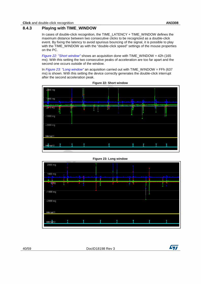
8.4.3 Playing with TIME_WINDOW In cases of double-click recognition, the TIME_LATENCY + TIME_WINDOW defines the maximum distance between two consecutive clicks to be recognized as a double-click event. By fixing the latency to avoid spurious bouncing of the signal, it is possible to play with the TIME_WINDOW as with the “double-click speed” settings of the mouse properties on the PC.
Figure 22: "Short window" shows an acquisition done with TIME_WINDOW = 42h (165 ms). With this setting the two consecutive peaks of acceleration are too far apart and the second one occurs outside of the window.
In Figure 23: "Long window" an acquisition carried out with TIME_WINDOW = FFh (637 ms) is shown. With this setting the device correctly generates the double-click interrupt after the second acceleration peak.
Figure 22: Short window
Figure 23: Long window

AN3308 First-in first-out (FIFO) buffer
DocID18198 Rev 3 41/59
9 First-in first-out (FIFO) buffer In order to limit intervention by the host processor and facilitate post processing data for recognition of events, the LIS3DH embeds a first-in first-out buffer (FIFO) for each of the three output channels, X, Y, and Z.
FIFO use allows consistent power saving for the system, it can wake up only when needed and burst the significant data out from the FIFO.
The FIFO buffer can work according to four different modes that guarantee a high level of flexibility during application development: Bypass mode, FIFO mode, Stream mode, and Stream-to-FIFO mode.
The programmable watermark level and FIFO overrun event can be enabled to generate dedicated interrupts on the INT1 pin.
9.1 FIFO description The FIFO buffer is able to store up to 32 acceleration samples for each channel; data are stored in the 16-bit 2’s complement left-justified representation. The resolution is dependent on the power mode selected.
The data sample sets consist of 6 bytes (X_low, X_high, Y_low, Y_high, Z_low and Z_high) and they are released to the FIFO at the selected output data rate (ODR).
The new sample set is placed in the first empty FIFO slot until the buffer is full, therefore, the oldest value is overwritten.
Table 35: FIFO buffer full representation (32nd sample set stored)
Output registers 0x28h 0x29h 0x2Ah 0x2Bh 0x2Ch 0x2Dh
X_low(0) X_high(0) Y_low(0) Y_high(0) Z_low(0) Z_high(0)
FIFO index FIFO sample set
FIFO(0) X_low(0) X_high(0) Y_low(0) Y_high(0) Z_low(0) Z_high(0)
FIFO(1) X_low(1) X_high(1) Y_low(1) Y_high(1) Z_low(1) Z_high(1)
FIFO(2) X_low(2) X_high(2) Y_low(2) Y_high(2) Z_low(2) Z_high(2)
FIFO(3) X_low(3) X_high(3) Y_low(3) Y_high(3) Z_low(3) Z_high(3)
... ... ... ... ... ... ...
FIFO(30) X_low(30) X_high(30) Y_low(30) Y_high(30) Z_low(30) Z_high(30)
FIFO(31) X_low(31) X_high(31) Y_low(31) Y_high(31) Z_low(31) Z_high(31)

First-in first-out (FIFO) buffer AN3308
42/59 DocID18198 Rev 3
Table 36: FIFO overrun representation (33rd sample set stored and 1st sample discarded)
Output registers 0x28h 0x29h 0x2Ah 0x2Bh 0x2Ch 0x2Dh
X_low(1) X_high(1) Y_low(1) Y_high(1) Z_low(1) Z_high(1)
FIFO index FIFO sample set
FIFO(0) X_low(1) X_high(1) Y_low(1) Y_high(1) Z_low(1) Z_high(1)
FIFO(1) X_low(2) X_high(2) Y_low(2) Y_high(2) Z_low(2) Z_high(2)
FIFO(2) X_low(3) X_high(3) Y_low(3) Y_high(3) Z_low(3) Z_high(3)
FIFO(3) X_low(4) X_high(4) Y_low(4) Y_high(4) Z_low(4) Z_high(4)
... ... ... ... ... ... ...
FIFO(30) X_low(31) X_high(31) Y_low(31) Y_high(31) Z_low(31) Z_high(31)
FIFO(31) X_low(32) X_high(32) Y_low(32) Y_high(32) Z_low(32) Z_high(32)
Table 35: "FIFO buffer full representation (32nd sample set stored)" represents the FIFO full status when 32 samples are stored in the buffer while Table 36: "FIFO overrun representation (33rd sample set stored and 1st sample discarded)" represents the next step when the 33rd sample is inserted into FIFO and the 1st sample is overwritten. The new oldest sample set is made available in the output registers.
When FIFO is enabled and the mode is different from Bypass, the LIS3DH output registers (28h to 2Dh) always contain the oldest FIFO sample set.

AN3308 First-in first-out (FIFO) buffer
DocID18198 Rev 3 43/59
9.2 FIFO registers The FIFO buffer is managed by three different accelerometer registers, two of these allow enabling and configuring the FIFO behavior, the third provides information about the buffer status.
9.2.1 CTRL_REG5 (0x24) The FIFO_EN bit in CTRL_REG5 must be set to 1 in order to enable the internal first-in first-out buffer; when this bit is set, the accelerometer output registers (28h to 2Dh) don’t contain the current acceleration value but they always contain the oldest value stored in FIFO.
Table 37: FIFO enable bit in CTRL_REG5 b7 b6 b5 b4 b3 b2 b1 b0
X FIFO_EN X X X X X X
Figure 24: FIFO_EN connection block diagram
FIFOBuffer
ADC
Output Registers0
1
CTRL_REG5 (FIFO_EN)
MeasurementChain
FIFOBuffer
ADC
Output Registers0
1
CTRL_REG5 (FIFO_EN)

First-in first-out (FIFO) buffer AN3308
44/59 DocID18198 Rev 3
9.2.2 FIFO_CTRL_REG (0x2E) This register is dedicated to FIFO mode selection and watermark configuration.
Table 38: FIFO_CTRL_REG b7 b6 b5 b4 b3 b2 b1 b0
FM1 FM0 TR FTH4 FTH3 FTH2 FTH1 FTH0
The FM[1:0] bits define the selection of the behavior of the FIFO buffer:
1. FM[1:0] = (0,0): Bypass mode 2. FM[1:0] = (0,1): FIFO mode 3. FM[1:0] = (1,0): Stream mode 4. FM[1:0] = (1,1): Stream-to-FIFO mode
The trigger used to activate Stream-to-FIFO mode is related to the IA bit value of the selected INT1_SRC register and does not depend on the interrupt pin value and polarity. The trigger is generated also if the selected interrupt is not driven to an interrupt pin.
FTH[4:0] bits define the watermark level; when FIFO content exceeds this value the WTM bit is set to “1” in the FIFO source register.
9.2.3 FIFO_SRC_REG (0x2F) This register is updated at every ODR and provides information about the FIFO buffer status.
Table 39: FIFO_SRC_REG b7 b6 b5 b4 b3 b2 b1 b0
WTM OVRN_
FIFO EMPTY FSS4 FSS3 FSS2 FSS1 FSS0
• WTM bit is set high when FIFO content exceeds watermark level. • OVRN_FIFO bit is set high when the FIFO buffer is full, which means that the FIFO
buffer contains 32 unread samples. At the following ODR a new sample set replaces the oldest FIFO value. The OVRN_FIFO bit is reset when the first sample set has been read.
• EMPTY flag is set high when all FIFO samples have been read and the FIFO is empty.
• FSS[4:0] field always contains the current number of unread samples stored in the FIFO buffer. When FIFO is enabled, this value increases at ODR frequency until the buffer is full, whereas it decreases every time that one sample set is retrieved from FIFO.

AN3308 First-in first-out (FIFO) buffer
DocID18198 Rev 3 45/59
Register content is updated synchronous to the FIFO write and read operation. Table 40: FIFO_SRC_REG behavior assuming FTH[4:0] = 15
WTM OVRN_FIFO EMPTY FSS[4:1] Unread FIFO samples Timing
0 0 1 00000 0 t0
0 0 0 00001 1 t0 + 1/ODR
0 0 0 00010 2 t0 + 2/ODR
... ... ... ... ... ...
0 0 0 01111 15 t0 + 15/ODR
1 0 0 10000 16 t0 + 16/ODR
... ... ... ... ... ...
1 0 0 11110 30 t0 + 30/ODR
1 0 0 11111 31 t0 + 31/ODR
1 1 0 11111 32 t0 + 32/ODR
The watermark flag and FIFO overrun event can be enabled to generate a dedicated interrupt on the INT1 pin by configuring CTRL_REG3.
Table 41: CTRL_REG3 (0x22) b7 b6 b5 b4 b3 b2 b1 b0
X X X X X I1_WTM I1_OVERRUN X
• I1_WTM bit drives watermark flag (WTM) on the INT1 pin. • I1_OVERRUN bit drives the overrun event (OVRN) on the INT1 pin.
If both bits are set to “1”, the INT1 pin status is the logical OR combination of the two signals.

First-in first-out (FIFO) buffer AN3308
46/59 DocID18198 Rev 3
9.3 FIFO modes The LIS3DH FIFO buffer can be configured to operate in four different modes selectable by the FM[1:0] field in FIFO_CTRL_REG. Available configurations ensure a high level of flexibility and extend the number of functions usable in application development.
Bypass, FIFO, Stream, and Stream-to-FIFO modes are described in the following paragraphs.
9.3.1 Bypass mode When Bypass mode is enabled, FIFO is not operational: buffer content is cleared, output registers (0x28 to 0x2D) are frozen at the last value loaded, and the FIFO buffer remains empty until another mode is selected.
Follow these steps for Bypass mode configuration:
1. Turn on FIFO by setting the FIFO_EN bit to “1” in CTRL_REG5 (0x24). After this operation the FIFO buffer is enabled but isn’t collecting data, output registers are frozen to the last samples set loaded.
2. Activate Bypass mode by setting the FM[1:0] field to “00” in FIFO_CTRL_REG (0x2E). If this mode is enabled, FIFO_SRC_REG (0x2F) is forced equal to 0x20.
Bypass mode must be used in order to stop and reset the FIFO buffer when a different mode is operating. Note that placing the FIFO buffer into Bypass mode clears the whole buffer content.
9.3.2 FIFO mode In FIFO mode, the buffer continues filling until full (32 sample sets stored,) then it stops collecting data and the FIFO content remains unchanged until a different mode is selected.
Follow these steps for FIFO mode configuration:
1. Turn on FIFO by setting the FIFO_EN bit to “1” in CTRL_REG5 (0x24). After this operation the FIFO buffer is enabled but isn’t collecting data, output registers are frozen to the last samples set loaded.
2. Activate FIFO mode by setting the FM[1:0] field to “01” in the FIFO_CTRL_REG (0x2E).
By selecting this mode, FIFO starts data collection and FIFO_SRC_REG (0x2F) changes according to the number of samples stored. At the end of the procedure, FIFO_SRC_REG is set to 0xDF and the OVRN flag generates an interrupt if the I1_OVERRUN bit is selected in CTRL_REG5. Data can be retrieved when OVRN_FIFO is set to”1”, performing a 32 sample set reading from the output registers, data can be retrieved also on the WTM flag instead of OVRN_FIFO if the application requires a lower number of samples. Communication speed is not so important in FIFO mode because data collection is stopped and there is no risk of overwriting acquired data. Before restarting FIFO mode, at the end of the reading procedure it is necessary to exit Bypass mode.
A FIFO mode recommendation is as follows:
1. Set FIFO_EN = 1: enable FIFO 2. Set FM[1:0] = (0,1): enable FIFO mode 3. Wait for OVRN_FIFO or WTM interrupt 4. Read data from accelerometer output registers 5. Set FM[1:0] = (0,0): enable Bypass mode 6. Repeat from step 2

AN3308 First-in first-out (FIFO) buffer
DocID18198 Rev 3 47/59
Figure 25: FIFO mode behavior
If FIFO mode is enabled, the buffer starts to collect data and fill all the 32 slots (from F0 to F31) at the selected output data rate. When the buffer is full, the OVRN_FIFO bit goes high and data collection is permanently stopped; the user can decide to read FIFO content at any time because it is maintained unchanged until Bypass mode is selected. The reading procedure is composed of a set of 32 samples of 6 bytes for a total of 192 bytes and retrieves data starting from the oldest sample stored in FIFO (F0). The OVRN_FIFO bit is reset when the first sample set has been read. Setting to Bypass mode resets FIFO and allows the user to enable FIFO mode again.
9.3.3 Stream mode In Stream mode FIFO continues filling, when the buffer is full, the FIFO index restarts from the beginning and older data is replaced by the current. The oldest values continue to be overwritten until a read operation frees FIFO slots. The reading speed of the host processor is essential in order to free slots faster than new data is made available. FM[1:0] Bypass configuration is used to stop this mode.
Follow these steps for FIFO mode configuration:
1. Turn on FIFO by setting the FIFO_EN bit to “1” in CTRL_REG5 (0x24). After this operation the FIFO buffer is enabled but isn’t collecting data, output registers are frozen to the last samples set loaded.
2. Activate Stream mode by setting the FM[1:0] field to “10” in FIFO_CTRL_REG (0x2E).
As described, for FIFO mode, data can be retrieved when OVRN_FIFO is set to “1” performing a 32 sample set reading from the output registers. Data can be retrieved also on the WTM flag if the application requires a smaller number of samples.
tFIFO mode
enableFIFOs
FIFO Modeenable
Start FIFOReading
FIFOBypass
…3332…31……543210…F1F0F0F0…F31……F5F4F3F2F1F0
t
stop
OVRN_FIFO
FIFO Reading
…3332…31……543210…F1F0…F31……F5F4F3F2F1F0

First-in first-out (FIFO) buffer AN3308
48/59 DocID18198 Rev 3
Figure 26: Stream mode fast reading behavior
In Stream mode, the FIFO buffer is continuously filling (from F0 to F31) at the selected output data rate. When the buffer is full, the OVRN_FIFO flag goes high and the recommended solution is to read all FIFO samples (192 bytes) faster then 1*ODR, in order to free FIFO slots for the new acceleration samples. This allows avoiding loss of data and limiting intervention by the host processor in order to increase efficiency of the system. If the reading procedure is not fast enough, three different cases can be observed:
1. FIFO sample set (6 bytes) reading faster than 1*ODR: data are correctly retrieved because a free slot is made available before new data is generated.
2. FIFO sample set (6 bytes) reading synchronous to 1*ODR: data are correctly retrieved because a free slot is made available before new data is generated but FIFO benefits are not exploited. This case is equivalent to reading data on data-ready interrupt and does not limit intervention of the host processor compared to the standard accelerometer reading.
3. FIFO sample set (6 bytes) reading slower than 1*ODR: in this case some data is lost because data recovery is not fast enough to free slots for new acceleration data Figure 27: "Stream mode slow reading behavior". The number of correctly recovered samples is related to the difference between the current ODR and the FIFO sample set reading rate.
Figure 27: Stream mode slow reading behavior
tStreamenable
OVRN_FIFO
FIFO Reading
Start FIFOReading
Start FIFOReading
……656463…333231……543210……F1F0F31…F1F0F31……F5F4F3F2F1F0
t
……656463…333231……543210……F1F0F31…F1F0F31……F5F4F3F2F1F0
tStreamenable
OVRN_FIFO
FIFO Reading
Start FIFOReading
Start FIFOReading
.
.…yyxx…656463.kk→yyjj →xx3231……3210…F?+1F?…F1F0F31.F?+1F?F0F31……F3F2F1F0
Samplesoverwritten
t
.
.…yyxx…656463.kk→yyjj →xx3231……3210…F?+1F?…F1F0F31.F?+1F?F0F31……F3F2F1F0

AN3308 First-in first-out (FIFO) buffer
DocID18198 Rev 3 49/59
In Figure 27: "Stream mode slow reading behavior", due to slow reading, data from “jj” are not retrieved because they are replaced by the new accelerometer samples generated by the system.
Figure 28: Stream mode slow reading zoom
After enabling Stream mode, FIFO slots are filled at the end of each ODR time frame. The reading procedure must start as soon as the OVRN flag is set to “1”, data are retrieved from FIFO at the beginning of the read. When a read command is sent to the device, the content of the output registers is moved to the SPI/I2C register and the current oldest FIFO value is shifted into the output registers in order to allow the next read. In the case of a read slower than 1*ODR, some data can be retrieved from FIFO after that new sample is inserted into the addressed location. In Figure 28: "Stream mode slow reading zoom" the fourth read command starts after the refresh of the F3 index and this generates a disconnect in the reading data. The OVRN flag advises the user that this event has taken place. In this example, three correct samples have been read, the number of correctly recovered samples is dependent on the difference between the current ODR and the FIFO sample set reading timeframe.
9.3.4 Stream-to-FIFO mode This mode is a combination of the Stream and FIFO modes described above. In Stream-to-FIFO mode, the FIFO buffer starts operating in Stream mode and switches to FIFO mode when the selected interrupt occurs.
Follow these steps for Stream-to-FIFO mode configuration:
1. Configure the desired interrupt generator using register INT1_CFG (0x30). 2. Set the TR bit in FIFO_CTRL_REG (0x2E) according to the configured interrupt
generator: TR = “0” in order to select interrupt 1, TR = “1” in order to select interrupt 2. 3. Turn on FIFO by setting the FIFO_EN bit to “1” in CTRL_REG5 (0x24). After this
operation the FIFO buffer is enabled but isn’t collecting data, output registers are frozen to the last samples set loaded.
4. Activate Stream-to-FIFO mode by setting the FM[1:0] field to “11” in FIFO_CTRL_REG (0x2E).
The interrupt trigger is related to the IA bit in the INT1_SRC register and it is generated even if the interrupt signal is not driven to an interrupt pad. A mode switch is performed if both IA and OVRN_FIFO bits are set high. Stream-to-FIFO mode is sensitive to the trigger level and not to the trigger edge, this means that if Stream-to-FIFO is in FIFO mode and the interrupt condition disappears, the FIFO buffer returns to Stream mode because the IA bit becomes zero. It is recommended to latch the interrupt signal used as the FIFO trigger in order to avoid losing interrupt events. If the selected interrupt is latched, register
Streamenable
t
OVRN_FIFO
R0:0FIFO Reading
Start FIFOReading
Samplesoverwritten
……363534333231…43210……F4F3F2F1F0F31…F4F3F2F1F0
R1:1 R2:2 R3:35 R4:36
t0
t0+dt t0+31dtt
R0:0
……363534333231…43210……F4F3F2F1F0F31…F4F3F2F1F0
R1:1 R2:2 R3:35 R4:36
t0

First-in first-out (FIFO) buffer AN3308
50/59 DocID18198 Rev 3
INT1_SRC must be read in order to clear the IA bit; after reading, the IA bit takes 2*ODR to go low.
In Stream mode the FIFO buffer continues filling, when the buffer is full, the OVRN_FIFO bit is set high and the next samples overwrite the oldest. When a trigger occurs, two different cases can be observed:
1. If the FIFO buffer is already full (OVRN_FIFO = “1”), it stops collecting data at the first sample after the trigger. FIFO content is composed of #30 samples collected before the trigger event, the sample that has generated the interrupt event and one sample after the trigger.
2. If FIFO isn’t yet full (initial transient), it continues filling until it is full (OVRN_FIFO = “1”) and then, if the trigger is still present, it stops collecting data.
Figure 29: Stream-to-FIFO mode: interrupt not latched
Figure 30: Stream-to-FIFO mode: interrupt latched
Stream-to-FIFO can be used in order to analyze the sample history that generated an interrupt; the standard operation is to read FIFO content when FIFO mode is triggered and the FIFO buffer is full and stopped.
Trigger (IA bit)
tStream to FIFO
enableFIFOstop
OVRN_FIFO
FIFO Reading
Start FIFOReading
ODR
3534333231……543210F32F1F0
Interrupt lostt
3534333231……543210F32F1F0
Trigger (IA bit)t
Stream-to-FIFOenable
FIFOstop
OVRN_FIFO
Stream-to-FIFOenable
ReadINT SRC
FIFO Reading
Start FIFOReading
FIFOBypass
3231……543210F0F0F0F31F5F4F3F2F1F0
t
3231……543210F0F0F0F31F5F4F3F2F1F0

AN3308 First-in first-out (FIFO) buffer
DocID18198 Rev 3 51/59
9.4 Watermark The watermark is a configurable flag that can be used to generate a specific interrupt in order to know when the FIFO buffer contains the minimum number of samples defined as the watermark level. The user can select the desired level in a range from 0 to 31 using the FTH[4:0] field in FIFO_CTRL_REG while FIFO_SRC_REG FSS[4:0] always contains the number of samples stored in FIFO.
If FSS[4:0] is greater than FTH[4:0], the WTM bit is set high in FIFO_SRC_REG, on the contrary, WTM is driven low when the FSS[4:0] field becomes lower than FTH[4:0]. FSS[4:0] increases by one step at the ODR frequency and decreases by one step every time that a sample set reading is performed by the user.
Figure 31: Watermark behavior - FTH[4:0] = 10
In Figure 31: "Watermark behavior - FTH[4:0] = 10", the first row indicates the FSS[4:0] value, the second row indicates the relative FIFO slot and last row shows the incremental FIFO data. Assuming FTH[4:0] = 10, the WTM flag changes from “0” to “1” when the eleventh FIFO slot is filled (F10). Figure 32: "FIFO reading diagram - FTH[4:0] = 10" shows that the WTM flag goes low when the FIFO content is less than FTH[4:0], it means that nine unread sample sets remain in FIFO.
The watermark flag (WTM) can be enabled to generate a dedicated interrupt on the INT1 pin by setting the I1_WTM bit high in CTRL_REG3.
tFIFO
enable
OVRN_FIFO
131+OVRN31…..1211……654321
323130……1110……543210F0F31F30……F11F10……F5F4F3F2F1F0
WTM
FIFO Reading
Start FIFOReading
t
131+OVRN31…..1211……654321
323130……1110……543210F0F31F30……F11F10……F5F4F3F2F1F0

First-in first-out (FIFO) buffer AN3308
52/59 DocID18198 Rev 3
9.5 Retrieving data from FIFO When FIFO is enabled and the mode is different from Bypass, reading output registers (28h to 2Dh) returns the oldest FIFO sample set.
Whenever output registers are read, their content is moved to the SPI/I2C output buffer. FIFO slots are ideally shifted up one level in order to release room for a new sample reception and output registers load the current oldest value stored in the FIFO buffer.
The whole FIFO content is retrieved by performing thirty-two reads from the accelerometer output registers, every other read returns the same last value until a new sample set is available in the FIFO buffer.
Data can be retrieved from FIFO using every reading byte combination in order to increase the application flexibility (ex: 196 single byte reads, 32 reads of 6 bytes, 1 multiple read of 196 bytes, etc.).
It is recommended to read all FIFO slots in a multiple byte read of 196 bytes (6 output registers by 32 slots) faster than 1*ODR. In order to minimize communication between the master and slave the read address is automatically updated by the device; it rolls back to 0x28 when register 0x2D is reached.
In order to avoid losing data, the right ODR must be selected according to the serial communication rate available. In the case of standard I2C mode being used (max rate 100 kHz), a single sample set reading takes 830 µs while total FIFO download is about 17.57 ms. I2C speed is lower than SPI and it needs about 29 clock pulses to start communication (Start, Slave Address, Device Address+Write, Restart, Device Address+Read) plus an additional 9 clock pulses for every byte to read. If this recommendation were followed, the complete FIFO reading would be performed faster than 1*ODR, which means that using a standard I2C, the selectable ODR must be lower than 57 Hz. If a fast I2C mode is used (max rate 400 kHz), the selectable ODR must be lower than 228 Hz.
Figure 32: FIFO reading diagram - FTH[4:0] = 10
In Figure 32: "FIFO reading diagram - FTH[4:0] = 10" “Rx” indicates a 6-byte read and “F0*” represents a single ODR slot expanded for better visibility.
Note: In order to set the EMPTY bit to '1', an additional sample (oldest one repeated) must be read and discarded.
tFIFO
enable
OVRN_FIFO
…3231+OVRN…11…1
…34333231…10…0…F2F1F0*F31…F10…F0
WTM
FIFO Reading
Start FIFOReading
R1 … … R22 … R30 R31 R0
30 29 … … 8 … 0+EMPTY
FIFO Empty
0+
EMPTY
01 1 …3231+OVRN…11…1
…34333231…10…0…F2F1F0*F31…F10…F0
… … … R29
… … 8 … 0+EMPTY 1
R0

AN3308 Activity / Inactivity recognition
DocID18198 Rev 3 53/59
10 Activity / Inactivity recognition The Activity/Inactivity recognition function allows reducing system power consumption and developing new smart applications.
When the Activity/Inactivity recognition function is activated, the device is able to automatically decrease the accelerometer sampling rate to 10 Hz low power, increasing the accelerometer ODR and bandwidth as soon as the wake-up interrupt event has been detected.
With this feature the system may be efficiently switched from low-power consumption to full performance and vice-versa depending on user-selectable acceleration events, thus ensuring power saving and flexibility.
The Activity/Inactivity recognition function is enabled by writing a wake-up threshold value different from zero in register ACT_THS. The return-to-sleep time is also customizable, acting on register ACT_DUR.
Figure 33: Activity / Inactivity recognition

Activity / Inactivity recognition AN3308
54/59 DocID18198 Rev 3
Figure 34: Activity / Inactivity duration
The user can also route the status (activity/inactivity) of the system to the INT2 pin by setting to 1 bit I2_ACT in CTRL_REG6. With this feature INT2 is high when the system is in inactivity ( ODR at 10 Hz ) and goes low when the system is in Activity (user ODR). The INT_POLARITY bit controls the polarity of the Activity / Inactivity signal.

AN3308 Auxiliary ADC and temperature sensor
DocID18198 Rev 3 55/59
11 Auxiliary ADC and temperature sensor The LIS3DH contains an auxiliary ADC with 3 separate dedicated inputs: pins ADC1, ADC2, ADC3.
The user can retrieve the converted data from registers OUT_ADC1_L (08h), OUT_ADC1_H (09h), OUT_ADC2_L (0Ah), OUT_ADC2_H (0Bh) and OUT_ADC3_L (0Ch), OUT_ADC3_H (0Dh).
In order to use the auxiliary ADC, the user must set the BDU bit (bit 7) to 1 in CTRL_REG4 (23h) and the ADC_EN bit (bit 7) to 1 in TEMP_CFG_REG (1Fh). The ADC sampling frequency is the same as that of the ODR in CTRL_REG1 (20h).
The input range is 1200 mV ±400 mV and the data output is expressed in 2's complement left-aligned.
The ADC resolution is 10 bits if the LPen (bit 3) in CTRL_REG1 (20h) is cleared (high-resolution / normal mode), otherwise, in low-power mode, the ADC resolution is 8-bit.
Channel 3 of the ADC can be connected to the temperature sensor by setting the TEMP_EN bit (bit 6) to 1 in TEMP_CFG_REG (1Fh). Refer to the LIS3DH datasheet for the conversion factor.

Accelerometer self-test procedure AN3308
56/59 DocID18198 Rev 3
12 Accelerometer self-test procedure The self-test allows the user to check the sensor functionality without moving it. When the self-test is enabled, an actuation force is applied to the sensor, simulating a definite input acceleration. In this case the sensor outputs will exhibit a change in their DC levels which are related to the selected full scale through the device sensitivity. When the self-test is activated, the device output level is given by the algebraic sum of the signals produced by the acceleration acting on the sensor and by the electrostatic test-force. If the output signals change within the given range (the min and max values are provided in the datasheet), then the sensor is working properly and the parameters of the interface chip are within the defined specifications. The self-test procedure is described in Figure 35: "Self-test procedure".
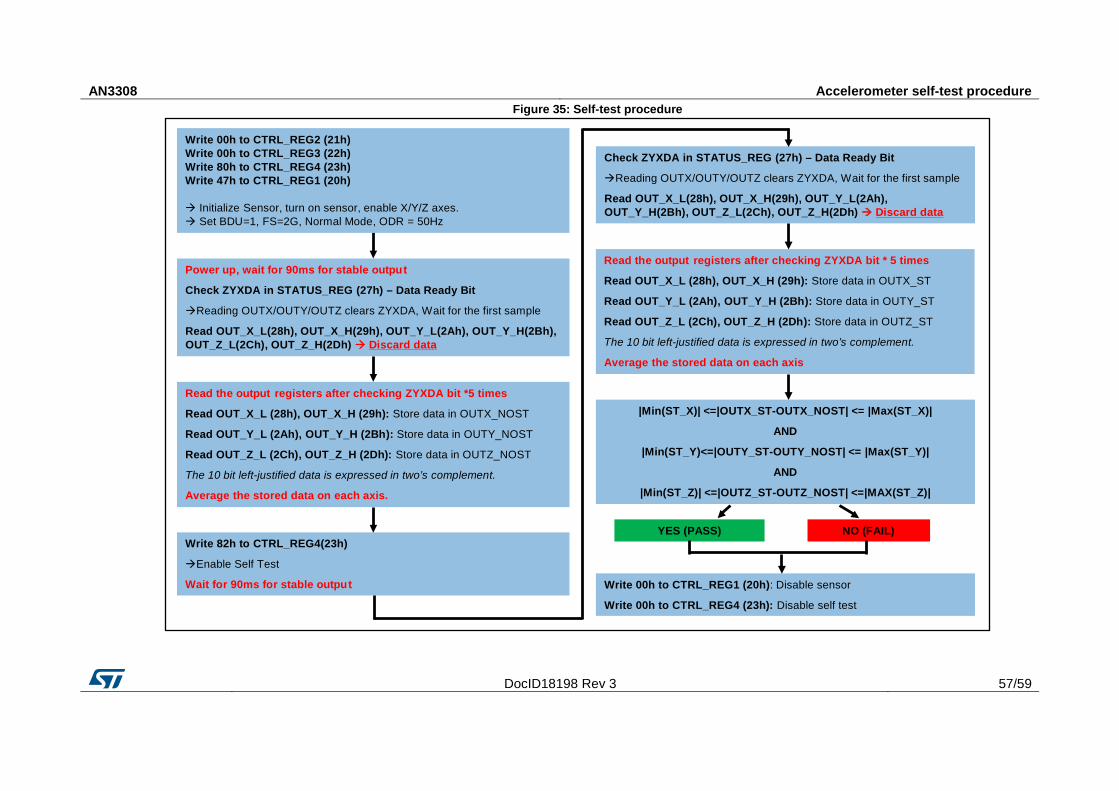
AN3308 Accelerometer self-test procedure
DocID18198 Rev 3 57/59
Figure 35: Self-test procedure
Power up, wait for 90ms for stable output
Check ZYXDA in STATUS_REG (27h) – Data Ready Bit
Reading OUTX/OUTY/OUTZ clears ZYXDA, Wait for the first sample
Read OUT_X_L(28h), OUT_X_H(29h), OUT_Y_L(2Ah), OUT_Y_H(2Bh),OUT_Z_L(2Ch), OUT_Z_H(2Dh) Discard data
Check ZYXDA in STATUS_REG (27h) – Data Ready Bit
Reading OUTX/OUTY/OUTZ clears ZYXDA, Wait for the first sample
Read OUT_X_L(28h), OUT_X_H(29h), OUT_Y_L(2Ah),OUT_Y_H(2Bh), OUT_Z_L(2Ch), OUT_Z_H(2Dh) Discard data
YES (PASS) NO (FAIL)
Write 00h to CTRL_REG1 (20h): Disable sensor
Write 00h to CTRL_REG4 (23h): Disable self test
Read the output registers after checking ZYXDA bit *5 times
Read OUT_X_L (28h), OUT_X_H (29h): Store data in OUTX_NOST
Read OUT_Y_L (2Ah), OUT_Y_H (2Bh): Store data in OUTY_NOST
Read OUT_Z_L (2Ch), OUT_Z_H (2Dh): Store data in OUTZ_NOST
The 10 bit left-justified data is expressed in two’s complement.
Average the stored data on each axis.
Write 82h to CTRL_REG4(23h)
Enable Self Test
Wait for 90ms for stable output
|Min(ST_X)| <=|OUTX_ST-OUTX_NOST| <= |Max(ST_X)|
AND
|Min(ST_Y)<=|OUTY_ST-OUTY_NOST| <= |Max(ST_Y)|
AND
|Min(ST_Z)| <=|OUTZ_ST-OUTZ_NOST| <=|MAX(ST_Z)|
Read the output registers after checking ZYXDA bit * 5 times
Read OUT_X_L (28h), OUT_X_H (29h): Store data in OUTX_ST
Read OUT_Y_L (2Ah), OUT_Y_H (2Bh): Store data in OUTY_ST
Read OUT_Z_L (2Ch), OUT_Z_H (2Dh): Store data in OUTZ_ST
The 10 bit left-justified data is expressed in two’s complement.
Average the stored data on each axis
Write 00h to CTRL_REG2 (21h)Write 00h to CTRL_REG3 (22h)Write 80h to CTRL_REG4 (23h)Write 47h to CTRL_REG1 (20h)
Initialize Sensor, turn on sensor, enable X/Y/Z axes. Set BDU=1, FS=2G, Normal Mode, ODR = 50Hz
Revision history AN3308
58/59 DocID18198 Rev 3
13 Revision history Table 42: Document revision history
Date Revision Changes
14-Jan-2011 1 Initial release.
27-Jan-2017 2
Updated Table 1: "Registers" Updated Section 2: "Operating modes" Updated Section 3: "Startup sequence" Updated Section 3.1.1: "Using the status register" Updated Section 3.1.2: "Using the data-ready (DRDY) signal" Updated Section 5: "Inertial interrupt" Updated Section 6: "6D/4D orientation detection" Updated Section 7: "Click and double-click recognition" Updated Section 8: "First-in first-out (FIFO) buffer" Added Section 9: "Activity / Inactivity recognition" Updated Section 10: "Auxiliary ADC and temperature sensor" Minor textual updates
08-Jun-2017 3
Updated Section 3.4: "High-resolution mode" and Section 8: "Click and double-click recognition" Updated Table 9: "Output data registers content vs. acceleration (FS = ±2 g, high-resolution mode)" and Table 22: "Truth table" Added Section 12: "Accelerometer self-test procedure"

AN3308
DocID18198 Rev 3 59/59
IMPORTANT NOTICE – PLEASE READ CAREFULLY
STMicroelectronics NV and its subsidiaries (“ST”) reserve the right to make changes, corrections, enhancements, modifications, and improvements to ST products and/or to this document at any time without notice. Purchasers should obtain the latest relevant information on ST products before placing orders. ST products are sold pursuant to ST’s terms and conditions of sale in place at the time of order acknowledgement.
Purchasers are solely responsible for the choice, selection, and use of ST products and ST assumes no liability for application assistance or the design of Purchasers’ products.
No license, express or implied, to any intellectual property right is granted by ST herein.
Resale of ST products with provisions different from the information set forth herein shall void any warranty granted by ST for such product.
ST and the ST logo are trademarks of ST. All other product or service names are the property of their respective owners.
Information in this document supersedes and replaces information previously supplied in any prior versions of this document.
© 2017 STMicroelectronics – All rights reserved