lithography at nufab
TRANSCRIPT

Lithography at NUFAB: For Beginners and the Experienced
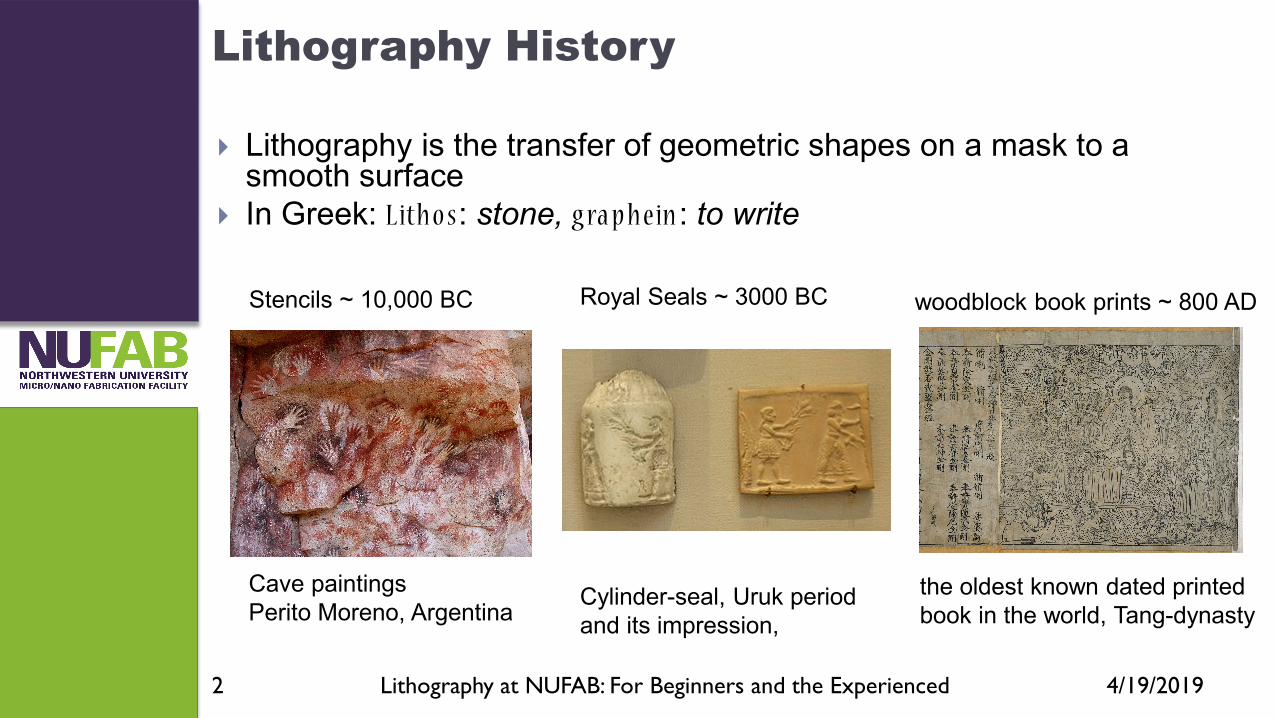
Lithography History
Lithography is the transfer of geometric shapes on a mask to a smooth surface
In Greek: Litho s: stone, g ra phein : to write
4/19/2019Lithography at NUFAB: For Beginners and the Experienced2
Stencils ~ 10,000 BC Royal Seals ~ 3000 BC woodblock book prints ~ 800 AD
Cave paintings Perito Moreno, Argentina
the oldest known dated printed book in the world, Tang-dynasty
Cylinder-seal, Uruk period and its impression,

Grandfather of the mask aligners
Photo(litho)graphy…- not the digital one -
First photographs by a pinhole camera on Silver Nitrate papers ~ 1840s
4/19/2019Lithography at NUFAB: For Beginners and the Experienced3
Anybody remember this?
Agrandisseur (Enlarger)

Chronology of photolithography in industry
4/19/2019Lithography at NUFAB: For Beginners and the Experienced4
Contact Lithography1st IC’s ~ 200 um resolution
Proximity lithography~ 2 um resolution Worse than contact but less defects and prolonged mask life
Step and repeatsubmicron resolution with image reductionNo contacts with the sample so long mask life
Contact lithography is still commonly practiced today, mainly in applications requiring thick photoresist and/or double-sided alignment and exposure. Advanced 3D packaging, optical devices, Microfluidics and MEMS applications..

Lithography Applications
4/19/2019Lithography at NUFAB: For Beginners and the Experienced5
Micro/Nano fluidics Flexible Electronics Bioelectronics and implantables
Biosensors NEMS - nano injector

Lithography Applications contd.
4/19/2019Lithography at NUFAB: For Beginners and the Experienced6
Solar Cells
MEMS
Electronic Devices
Integrated Circuits
Fitbit Accelerometer
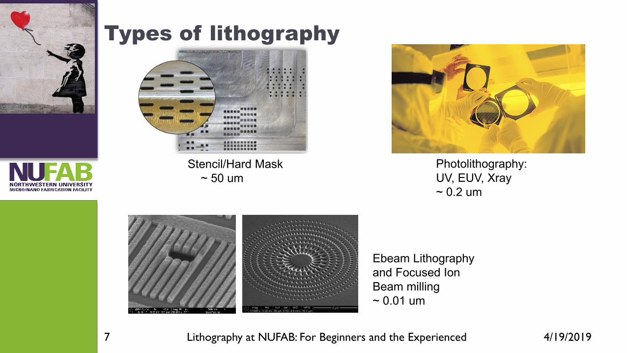
Types of lithography
4/19/2019Lithography at NUFAB: For Beginners and the Experienced7
Stencil/Hard Mask~ 50 um
Photolithography:UV, EUV, Xray~ 0.2 um
Ebeam Lithography and Focused Ion Beam milling~ 0.01 um

Photolithography ----- How it works
4/19/2019Lithography at NUFAB: For Beginners and the Experienced8

Required tools
4/19/2019Lithography at NUFAB: For Beginners and the Experienced9
Masks: Chromium or Iron oxide plates Mask aligner: typically has a UV sourcesuch as Hg lamp or UV LED
Substrates: Si wafers, glass slides, metal foils Photoresists Developers:
Alkaline or Solvent solutions
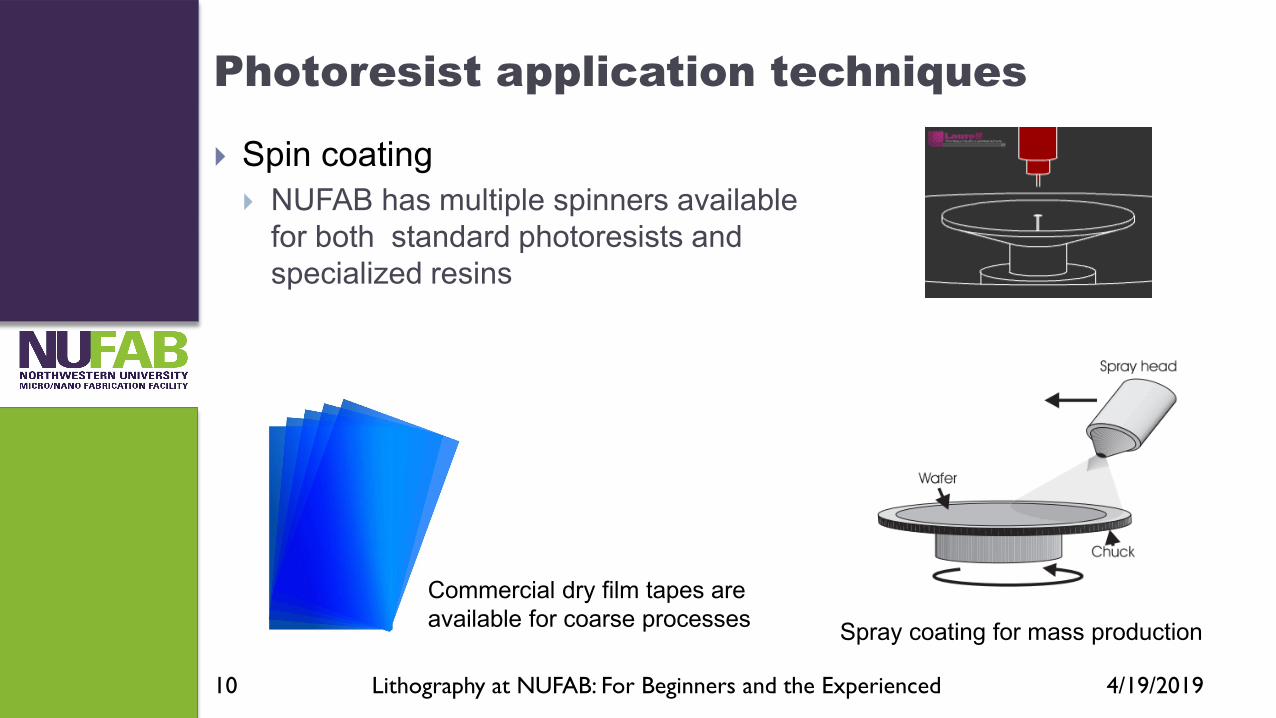
Photoresist application techniques
Spin coating NUFAB has multiple spinners available
for both standard photoresists and specialized resins
4/19/2019Lithography at NUFAB: For Beginners and the Experienced10
Commercial dry film tapes areavailable for coarse processes Spray coating for mass production

Photolithography types explained
4/19/2019Lithography at NUFAB: For Beginners and the Experienced11
Resolution 0.7 um 5 um 0.3 um

Photoresist developing techniques
4/19/2019Lithography at NUFAB: For Beginners and the Experienced12
NUFAB’s proposed automatic spin developing
station

Datasheets are good resources for recipes
4/19/2019Lithography at NUFAB: For Beginners and the Experienced13
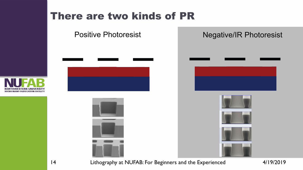
Positive Photoresist Negative/IR Photoresist
There are two kinds of PR
4/19/2019Lithography at NUFAB: For Beginners and the Experienced14
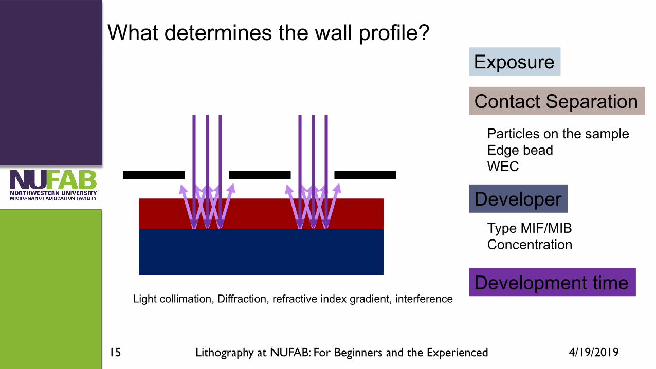
What determines the wall profile?Exposure
Contact Separation
Developer
Development time
Particles on the sampleEdge beadWEC
Type MIF/MIBConcentration
Light collimation, Diffraction, refractive index gradient, interference
4/19/2019Lithography at NUFAB: For Beginners and the Experienced15
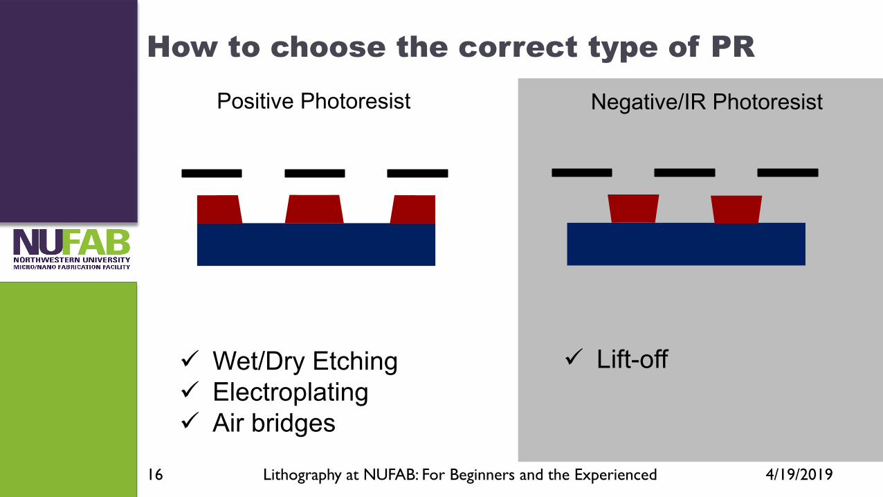
Positive Photoresist Negative/IR Photoresist
Wet/Dry Etching Electroplating Air bridges
Lift-off
How to choose the correct type of PR
4/19/2019Lithography at NUFAB: For Beginners and the Experienced16
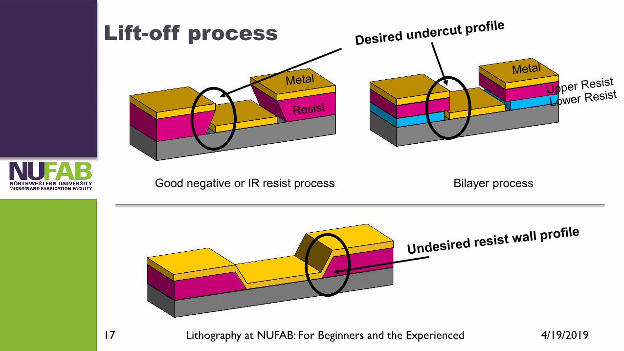
Lift-off process
4/19/2019Lithography at NUFAB: For Beginners and the Experienced17
Good negative or IR resist process Bilayer process

Lift-off – How it works
LOR 1A, 5A
4/19/2019Lithography at NUFAB: For Beginners and the Experienced18
Bilayer process Toluene or Chlorobenzene soaking
A positive PRS1805, S1813 etc.
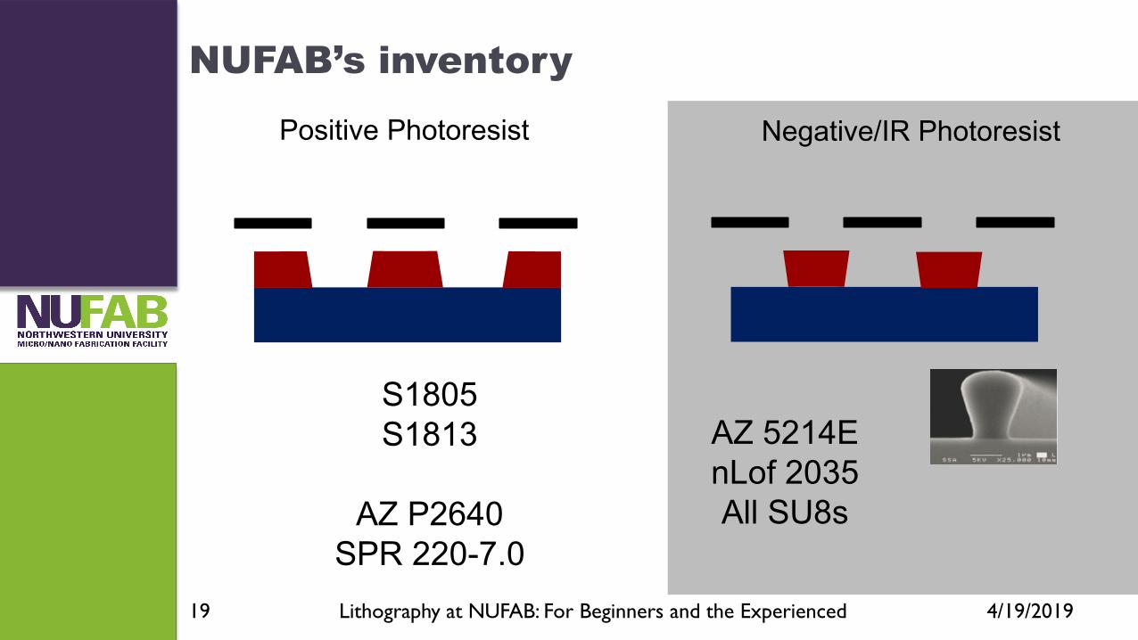
Positive Photoresist Negative/IR Photoresist
S1805S1813
AZ P2640SPR 220-7.0
AZ 5214EnLof 2035All SU8s
NUFAB’s inventory
4/19/2019Lithography at NUFAB: For Beginners and the Experienced19
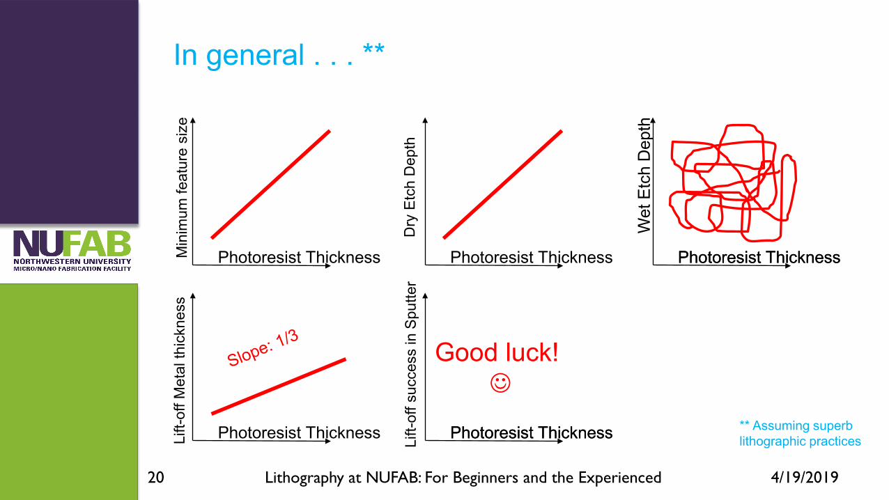
Min
imum
feat
ure
size
Photoresist Thickness
In general . . . **
** Assuming superb lithographic practices
Dry
Etc
h D
epth
Photoresist Thickness
Wet
Etc
h D
epth
Photoresist ThicknessPhotoresist Thickness
Lift-
off M
etal
thic
knes
s
Photoresist Thickness Lift-
off s
ucce
ss in
Spu
tter
Good luck!
Photoresist ThicknessPhotoresist Thickness
4/19/2019Lithography at NUFAB: For Beginners and the Experienced20
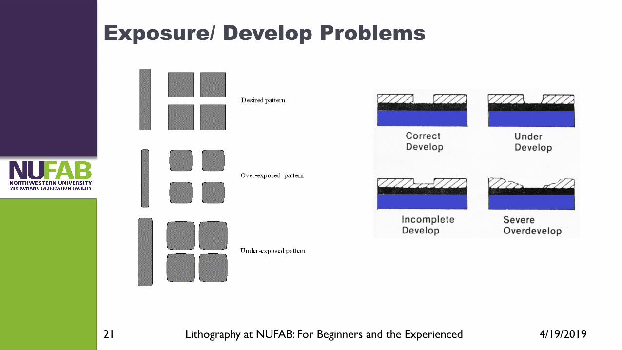
Exposure/ Develop Problems
4/19/2019Lithography at NUFAB: For Beginners and the Experienced21

Contact Problems
Wrong operation of the mask aligner
4/19/2019Lithography at NUFAB: For Beginners and the Experienced22
Desired pattern Resulting patternPhotoresist
Substrate
Severe edge beading
Substrate
Photoresist
Dirty mask/substrate

Designing Masks
DXF – AutoCAD Free for educational use widely available python/matlab friendly
Too complicated Not all tools are supported Resource heavy Lacks basic Boolean operations
GDSII – Ledit, Klayout, Layout editor De facto standard for
photolithography masks Fool proof Everything is supported Resource friendly
Decent editors are expensive Lacks circles
4/19/2019Lithography at NUFAB: For Beginners and the Experienced23

Mask materials
Chromium Opaque Better resolution Cheaper
Requires careful alignment mark design
Iron Oxide Transparent above 600 nm Acceptable resolution Forgiving to alignment mark
design errors
Expensive
4/19/2019Lithography at NUFAB: For Beginners and the Experienced24

Alignment marks are required for overlay exposures
4/19/2019Lithography at NUFAB: For Beginners and the Experienced25
2 um 0.2 um
Vernier mark
Accuracy
Simple marks for coarse alignment Complex marks for fine alignment
Microscope magnification, resolution and depth of field affect accuracy

NUFAB tools : Contact Aligners
Advanced contact modes UV lamp – 365 nm and 405 nm (h, i-line) Up to 6 inch wafer process Backside alignment
4/19/2019Lithography at NUFAB: For Beginners and the Experienced26
Suss MJB4 Suss MABA6

Digital age – “film to digital photography”
Maskless lithography Eliminates the need of
fabrication of a mask Fast and dynamic Suitable for prototyping
and rapid optimization
4/19/2019Lithography at NUFAB: For Beginners and the Experienced27

NUFAB tools: Maskless Aligners
375, 395 and 405 nm lasers Up to 150 x 150 mm writing area Backside alignment
4/19/2019Lithography at NUFAB: For Beginners and the Experienced28
Heidelberg uPG 501
Heidelberg MLA150

NUFAB tools: Laser Cutter
Virtually anything can be cut ~20 um spot size 15 um lines can be cut
depending on the material thickness
4/19/2019Lithography at NUFAB: For Beginners and the Experienced29
LPKF R Protolaser

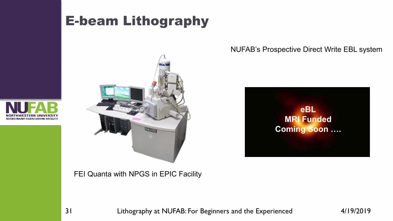
E-Beam Lithography
Write using electrons Less than 10 nm resolution E-beam resist instead of photoresist: PMMA, ZEP
4/19/2019Lithography at NUFAB: For Beginners and the Experienced30
Quantum electronics Plasmonics Metamaterials
E-beam Lithography
4/19/2019Lithography at NUFAB: For Beginners and the Experienced31
FEI Quanta with NPGS in EPIC Facility
NUFAB’s Prospective Direct Write EBL system
eBLMRI Funded
Coming Soon ….

Focused Ion Beam Milling
Scribes using ions High resolution etching
4/19/2019Lithography at NUFAB: For Beginners and the Experienced32
FEI Helios FIB in EPIC facility

Advanced topics: Optical limit Diffraction is the main limiting factor for better resolution
4/19/2019Lithography at NUFAB: For Beginners and the Experienced33
𝑀𝑀𝑀𝑀𝑀𝑀 𝐹𝐹𝐹𝐹𝐹𝐹𝐹𝐹𝐹𝐹𝐹𝐹𝐹𝐹 𝑆𝑆𝑀𝑀𝑆𝑆𝐹𝐹 ∝ 𝑘𝑘 × 𝜆𝜆 × 𝑔𝑔𝐹𝐹𝑔𝑔
k: constantλ: wavelength
Minimum size (um)
Gap(um)
2.7 20
1.9 10
1.35 5
0.6 1
Affect of increasing the gapon exposure profile
SubstratePhotoresist
Gap
0 um
15 um

Advanced topics: Material limit
Not all photoresists produce the same resolution due to different polymerization/crosslinking.
Each photoresist has different aspects ratio capability Most have at least aspect ratio of 2, Shipley S1800 series, AZ 5200
series Some have larger than 5, such as SU8 variants
4/19/2019Lithography at NUFAB: For Beginners and the Experienced34
NUFAB recommends using a photoresist thickness of at most half of the required minimum feature size to beginners and for most R&D applications as there are other factors involved.
Remarks
The fundamental limit of optical lithography is not determined by the optical system/lithography technique alone but rather is an overall contributions from the optics, resist, develop and etching processes.
Process window: Capability of printing small features does not always guarantee a good quality and a repeatable and controllable patterning.
Alignment: Alignment to the underlying layer is equally as important as the optics.
4/19/2019Lithography at NUFAB: For Beginners and the Experienced35

4/19/2019Lithography at NUFAB: For Beginners and the Experienced36
Questions?
