lm25118 wide voltage range buck-boost controller … · (8) fb vin (1) (16) vcc rt (3) (18) hb vout...
TRANSCRIPT

(8) FB
VIN (1) (16) VCC
RT (3)
(18) HB
VOUT
AGND (6)
PGND (14)
DAP (EP)
(13) CSG
RAMP (5)
SS (7)
(12) CS
(15) LO
(10) VOUT
(19) HO
(20) HS
(9) COMP
LM25118MH
VIN
EN (4)
SYNC (11)
VCCX (17)
UVLO (2)
ON
OFF
VEN(ON)
VEN(OFF)0V
0 10 20 30 40 50
VIN (V)
75
80
85
90
95
100
EF
FIC
IEN
CY
(%
)
1 AMP
2 AMP
xxxxxxxxxxxxxxxxxxxxxxxxxxxxxxx
xxxxxxxxxxxxxxxxxxxxxxxxxxxxx
xxxxxxxxxxxxxxxxxxxxxxxxxx
3 AMP
Product
Folder
Order
Now
Technical
Documents
Tools &
Software
Support &Community
An IMPORTANT NOTICE at the end of this data sheet addresses availability, warranty, changes, use in safety-critical applications,intellectual property matters and other important disclaimers. PRODUCTION DATA.
LM25118SNVS726F –JULY 2011–REVISED MARCH 2018
LM25118 Wide Voltage Range Buck-Boost Controller
1
1 Features1• Input Voltage Operating Range From 3 V to 42 V• Emulated Peak Current Mode Control• Smooth Transition Between Step-Down and Step-
Up Modes• Switching Frequency Programmable to 500 KHz• Oscillator Synchronization Capability• Internal High Voltage Bias Regulator• Integrated High and Low-Side Gate Drivers• Programmable Soft-Start Time• Ultra-Low Shutdown Current• Enable Input• Wide Bandwidth Error Amplifier• 1.5% Feedback Reference Accuracy• Thermal Shutdown• Package: 20-Pin HTSSOP (Exposed Pad)• Create a Custom Design Using the LM25118 With
the WEBENCH® Power Designer
2 ApplicationsIndustrial Buck-Boost Supplies
3 DescriptionThe LM25118 wide voltage range Buck-Boostswitching regulator controller features all of thefunctions necessary to implement a high-performance, cost-efficient Buck-Boost regulatorusing a minimum of external components. The Buck-Boost topology maintains output voltage regulationwhen the input voltage is either less than or greaterthan the output voltage making it especially suitablefor automotive applications. The LM25118 operatesas a buck regulator while the input voltage issufficiently greater than the regulated output voltageand gradually transitions to the buck-boost mode asthe input voltage approaches the output. This dual-mode approach maintains regulation over a widerange of input voltages with optimal conversionefficiency in the buck mode and a glitch-free outputduring mode transitions. This easy-to-use controllerincludes drivers for the high-side buck MOSFET andthe low-side boost MOSFET. The control method ofthe regulator is based upon current mode controlusing an emulated current ramp. Emulated currentmode control reduces noise sensitivity of the pulse-width modulation circuit, allowing reliable control ofthe very small duty cycles necessary in high inputvoltage applications. Additional protection featuresinclude current limit, thermal shutdown, and anenable input. The device is available in a power-enhanced, 20-pin HTSSOP package featuring anexposed die attach pad to aid thermal dissipation.
Device Information(1)
PART NUMBER PACKAGE BODY SIZE (NOM)LM25118 HTSSOP (20) 6.50 mm × 4.40 mm
(1) For all available packages, see the orderable addendum atthe end of the data sheet.
Simplified SchematicEfficiency vs VIN and IOUT, VOUT = 12 V

2
LM25118SNVS726F –JULY 2011–REVISED MARCH 2018 www.ti.com
Product Folder Links: LM25118
Submit Documentation Feedback Copyright © 2011–2018, Texas Instruments Incorporated
Table of Contents1 Features .................................................................. 12 Applications ........................................................... 13 Description ............................................................. 14 Revision History..................................................... 25 Pin Configuration and Functions ......................... 46 Specifications......................................................... 6
6.1 Absolute Maximum Ratings ...................................... 66.2 ESD Ratings.............................................................. 66.3 Recommended Operating Conditions....................... 66.4 Thermal Information .................................................. 66.5 Electrical Characteristics........................................... 76.6 Typical Characteristics ............................................ 10
7 Detailed Description ............................................ 127.1 Overview ................................................................. 127.2 Functional Block Diagram ....................................... 127.3 Feature Description................................................. 137.4 Device Functional Modes........................................ 21
8 Application and Implementation ........................ 238.1 Application Information............................................ 238.2 Typical Application .................................................. 23
9 Power Supply Recommendations ...................... 349.1 Bias Power Dissipation Reduction .......................... 349.2 Thermal Considerations .......................................... 35
10 Layout................................................................... 3510.1 Layout Guidelines ................................................. 3510.2 Layout Example .................................................... 35
11 Device and Documentation Support ................. 3611.1 Device Support...................................................... 3611.2 Receiving Notification of Documentation Updates 3611.3 Community Resources.......................................... 3611.4 Trademarks ........................................................... 3611.5 Electrostatic Discharge Caution............................ 3611.6 Glossary ................................................................ 36
12 Mechanical, Packaging, and OrderableInformation ........................................................... 37
4 Revision HistoryNOTE: Page numbers for previous revisions may differ from page numbers in the current version.
Changes from Revision E (July 2017) to Revision F Page
• Deleted roque text from ESD Ratings table. ......................................................................................................................... 6
Changes from Revision D (August 2014) to Revision E Page
• Moved the automotive device to a standalone data sheet (SNVSAX7) ................................................................................. 1• Changed language of WEBENCH list item; added additional content and links for WEBENCH further in data sheet ......... 1• Moved the storage temp parameters to the Absolute Maximum Ratings .............................................................................. 6• Changed junction temperature range from: ±150°C max to: –40°C to 150°C ...................................................................... 6• Changed Handling Ratings table to ESD Ratings .................................................................................................................. 6• Moved the junction temperature ranges in the Electrical Characteristics table to the test conditions statement .................. 7• Removed the VOLL minimum value ......................................................................................................................................... 8• Removed the VOLH minimum value......................................................................................................................................... 8• Added Community Resources section ................................................................................................................................ 36
Changes from Revision C (Novemeber 2013) to Revision D Page
• Changed data sheet flow and layout to conform with new TI standards. Added the following sections: DeviceInformation Table, Application and Implementation; Power Supply Recommendations; Layout; Device andDocumentation Support; Mechanical, Packaging, and Ordering Information ........................................................................ 1
• Changed Removed footnote to "VCC, LO, VCCX, UVLO to GND" ....................................................................................... 6
Changes from Revision B (April, 2013) to Revision C Page
• Deleted VIN Range on Functional Block Diagram................................................................................................................. 12• Changed Figure 19............................................................................................................................................................... 24• Changed VIN Specification................................................................................................................................................... 24

3
LM25118www.ti.com SNVS726F –JULY 2011–REVISED MARCH 2018
Product Folder Links: LM25118
Submit Documentation FeedbackCopyright © 2011–2018, Texas Instruments Incorporated
• Changed L1 Buck Mode Value............................................................................................................................................. 26• Changed IRIPPLE(BUCK) Value .................................................................................................................................................. 26• Changed Inductor Selection – L1 Text ................................................................................................................................. 26• Changed Equation 16........................................................................................................................................................... 26• Changed Equation 17........................................................................................................................................................... 26• Added Efficiency Parameter ................................................................................................................................................. 26• Changed I1(PEAK)Value........................................................................................................................................................... 27• Changed I2(PEAK) Value.......................................................................................................................................................... 27• Changed R13 = RSENSE Text ................................................................................................................................................ 27• Added Equation 20 .............................................................................................................................................................. 27• Added Equation 21 .............................................................................................................................................................. 27• Changed Equation 24 .......................................................................................................................................................... 27• Changed Equation 25 .......................................................................................................................................................... 27• Changed R13(BUCK) Value ..................................................................................................................................................... 27• Changed R13(BUCK-BOOST) Value ............................................................................................................................................ 27• Added Inductor Current Limit Calculation Section................................................................................................................ 28• Added Equation 29 .............................................................................................................................................................. 28• Added Equation 31 .............................................................................................................................................................. 28• Changed Equation 34........................................................................................................................................................... 28• Changed ESRMAX Value ....................................................................................................................................................... 28• Deleted Previous Equation 17 .............................................................................................................................................. 28• Deleted Previous Equation 18 .............................................................................................................................................. 28• Changed C1 – C5 = Input Capacitors Text .......................................................................................................................... 29• Changed R8, R9 Text........................................................................................................................................................... 30• Changed R1, R3, C21 Text .................................................................................................................................................. 30• Changed Equation 45 .......................................................................................................................................................... 30• Changed R4, C18, C17 Text ................................................................................................................................................ 31• Changed DMIN to DMAX in Equation 47.................................................................................................................................... 31• Changed DMAX Value ............................................................................................................................................................ 31• Changed DC Gain(MOD) Value............................................................................................................................................... 31• Changed ESRZERO Value...................................................................................................................................................... 31• Changed R4, C18, C17 Text ................................................................................................................................................ 32• Changed Figure 21............................................................................................................................................................... 33• Changed Figure 22............................................................................................................................................................... 33• Changed Figure 23............................................................................................................................................................... 33• Added Figure 24 ................................................................................................................................................................... 33• Added Figure 25 ................................................................................................................................................................... 33• Added Figure 26 ................................................................................................................................................................... 33
Changes from Revision A (March 2013) to Revision B Page
• Changed layout of National Data Sheet to TI format ........................................................................................................... 24

RT
RAMP
AGND
SS
HS
VCC
LO
PGND
EN
FB
COMP
VOUT
VIN
UVLO HO
HB
VCCX
CSG
CS
SYNC
1
2
3
4
8
7
6
5
9
10 11
12
13
14
15
16
17
18
19
20
Exposed Padon Bottom
(DAP)
4
LM25118SNVS726F –JULY 2011–REVISED MARCH 2018 www.ti.com
Product Folder Links: LM25118
Submit Documentation Feedback Copyright © 2011–2018, Texas Instruments Incorporated
5 Pin Configuration and Functions
PWP Package20-Pin HTSSOP With Exposed Pad
Top View
Pin FunctionsPIN TYPE
DESCRIPTIONNO. NAME1 VIN P/I Input supply voltage.
2 UVLO I
If the UVLO pin is below 1.23 V, the regulator will be in standby mode (VCC regulator running,switching regulator disabled). When the UVLO pin exceeds 1.23 V, the regulator enters thenormal operating mode. An external voltage divider can be used to set an undervoltageshutdown threshold. A fixed 5-µA current is sourced out of the UVLO pin. If a current limitcondition exists for 256 consecutive switching cycles, an internal switch pulls the UVLO pin toground and then releases.
3 RT I The internal oscillator frequency is set with a single resistor between this pin and the AGND pin.The recommended frequency range is 50 kHz to 500 kHz.
4 EN I If the EN pin is below 0.5 V, the regulator will be in a low power state drawing less than 10 µAfrom VIN. EN must be raised above 3 V for normal operation.
5 RAMP I Ramp control signal. An external capacitor connected between this pin and the AGND pin setsthe ramp slope used for emulated current mode control.
6 AGND G Analog ground.
7 SS I
Soft-Start. An external capacitor and an internal 10-µA current source set the rise time of theerror amp reference. The SS pin is held low when VCC is less than the VCC undervoltagethreshold (< 3.7 V), when the UVLO pin is low (< 1.23 V), when EN is low (< 0.5 V) or whenthermal shutdown is active.
8 FB I Feedback signal from the regulated output. Connect to the inverting input of the internal erroramplifier.
9 COMP O Output of the internal error amplifier. The loop compensation network should be connectedbetween COMP and the FB pin.
10 VOUT I Output voltage monitor for emulated current mode control. Connect this pin directly to theregulated output.
11 SYNC I Sync input for switching regulator synchronization to an external clock.12 CS I Current sense input. Connect to the diode side of the current sense resistor.13 CSG I Current sense ground input. Connect to the ground side of the current sense resistor.14 PGND G Power Ground.15 LO O Boost MOSFET gate drive output. Connect to the gate of the external boost MOSFET.
16 VCC P/I/O Output of the bias regulator. Locally decouple to PGND using a low ESR/ESL capacitor locatedas close to the controller as possible.

5
LM25118www.ti.com SNVS726F –JULY 2011–REVISED MARCH 2018
Product Folder Links: LM25118
Submit Documentation FeedbackCopyright © 2011–2018, Texas Instruments Incorporated
Pin Functions (continued)PIN TYPE
DESCRIPTIONNO. NAME
17 VCCX P/IOptional input for an externally supplied bias supply. If the voltage at the VCCX pin is greaterthan 3.9 V, the internal VCC regulator is disabled and the VCC pin is internally connected toVCCX pin supply. If VCCX is not used, connect to AGND.
18 HB IHigh-side gate driver supply used in bootstrap operation. The bootstrap capacitor suppliescurrent to charge the high-side MOSFET gate. This capacitor should be placed as close to thecontroller as possible and connected between HB and HS.
19 HO O Buck MOSFET gate drive output. Connect to the gate of the high side buck MOSFET through ashort, low inductance path.
20 HS I Buck MOSFET source pin. Connect to the source terminal of the high-side buck MOSFET andthe bootstrap capacitor.
— EP — Exposed thermal pad. Solder to the ground plane under the IC to aid in heat dissipation.

6
LM25118SNVS726F –JULY 2011–REVISED MARCH 2018 www.ti.com
Product Folder Links: LM25118
Submit Documentation Feedback Copyright © 2011–2018, Texas Instruments Incorporated
(1) Stresses beyond those listed under Absolute Maximum Ratings may cause permanent damage to the device. These are stress ratingsonly, which do not imply functional operation of the device at these or any other conditions beyond those indicated under RecommendedOperating Conditions. Exposure to absolute-maximum-rated conditions for extended periods may affect device reliability.
6 Specifications
6.1 Absolute Maximum Ratingsover operating free-air temperature range (unless otherwise noted) (1)
MIN MAX UNITVIN, EN, VOUT to GND –0.3 45 VVCC, LO, VCCX, UVLO to GND –0.3 16 VHB to HS –0.3 16 VHO to HS –0.3 HB + 0.3 VHS to GND –4 45 VCSG, CS to GND –0.3 0.3 VRAMP, SS, COMP, FB, SYNC, RT to GND –0.3 7 VJunction temperature –40 150 °CStorage temperature, Tstg –55 150 °C
(1) JEDEC document JEP155 states that 500-V HBM allows safe manufacturing with a standard ESD control process.(2) JEDEC document JEP157 states that 250-V CDM allows safe manufacturing with a standard ESD control process.
6.2 ESD RatingsVALUE UNIT
V(ESD) Electrostatic dischargeHuman-body model (HBM), per ANSI/ESDA/JEDEC JS-001 (1) ±2000
VCharged-device model (CDM), per JEDEC specification JESD22-C101 (2) ±1000
(1) Functional operation of the device and/or non-degradation at the Absolute Maximum Ratings or other conditions beyond those indicatedin the Recommended Operating Conditions is not implied. Operating Range conditions indicate the conditions at which the device isfunctional and the device should not be operated beyond such conditions. For ensured specifications and conditions, see ElectricalCharacteristics.
(2) VIN ≥ 5.0 V is required to initially start the controller.
6.3 Recommended Operating Conditionsover operating free-air temperature range (unless otherwise noted) (1)
MIN MAX UNITVIN (2) 3 42 VVCC, VCCX 4.75 14 VJunction temperature –40 +125 °C
(1) For more information about traditional and new thermal metrics, see the IC Package Thermal Metrics application report.(2) JEDEC 2-Layer test board (JESD 51-3)(3) JEDEC 4-Layer test board (JESD 51-7) with 4 thermal vias under the Exposed Pad(4) JEDEC 4-Layer test board (JESD 51-7) with 12 thermal vias under the Exposed Pad
6.4 Thermal Information
THERMAL METRIC (1)LM25118
UNITPWP (HTSSOP)20 PINS
RθJA Junction-to-ambient thermal resistance110 (2)
°C/W40 (3)
35 (4)
RθJC(bot) Junction-to-case (bottom) thermal resistance 4 °C/W

7
LM25118www.ti.com SNVS726F –JULY 2011–REVISED MARCH 2018
Product Folder Links: LM25118
Submit Documentation FeedbackCopyright © 2011–2018, Texas Instruments Incorporated
(1) Minimum and Maximum limits are ensured through test, design, or statistical correlation. Typical values represent the most likelyparametric norm at TJ = 25°C, and are provided for reference purposes only.
6.5 Electrical CharacteristicsUnless otherwise specified, the following conditions apply: VIN = 24 V, VCCX = 0 V, EN = 5 V, RT = 29.11 kΩ, no load on LOand HO. Typical values apply for TJ = 25°C; minimum and maximum values apply over the full junction temperature range foroperation: −40°C to +125°C. (1) (1)
PARAMETER TEST CONDITIONS MIN TYP MAX UNITVIN SUPPLY
IBIAS VIN operating current VCCX = 0 V 4.5 5.5 mAIBIASX VIN operating current VCCX = 5 V 1 1.85 mAISTDBY VIN shutdown current EN = 0 V 1 10 µA
VCC REGULATORVCC(REG) VCC regulation VCCX = 0 V 6.8 7 7.2 VVCC(REG) VCC regulation VCCX = 0 V, VIN = 6 V 5 5.25 5.5 V
VCC sourcing current limit VCC = 0 21 35 mAVCCX switch threshold VCCX rising 3.68 3.85 4.02 VVCCX switch hysterisis 0.2 VVCCX switch RDS(ON) ICCX = 10 mA 5 12 ΩVCCX switch leakage VCCX = 0 V 0.5 1 µAVCCCX pulldownresistance VCCX = 3 V 70 kΩ
VCC undervoltage lockoutvoltage VCC rising 3.52 3.7 3.86 V
VCC undervoltagehysterisis 0.21 V
HB DC bias current HB-HS = 15 V 205 260 µAVC LDO mode turnoff 10 V
EN INPUTVEN(OFF) EN input low threshold VEN falling 0.5 VVEN(ON) EN input high threshold VEN rising 3 V
EN input bias current VEN = 3 V –1 1 µAEN input bias current VEN = 0.5 V –1 1 µAEN input bias current VEN = 42 V 50 µA
UVLO THRESHOLDSUVLO UVLO standby threshold UVLO Rising 1.191 1.231 1.271 VΔUVLO UVLO threshold hysteresis 0.105 V
UVLO pullup currentsource UVLO = 0 V 5 µA
UVLO pulldown RDS(ON) 100 200 Ω

8
LM25118SNVS726F –JULY 2011–REVISED MARCH 2018 www.ti.com
Product Folder Links: LM25118
Submit Documentation Feedback Copyright © 2011–2018, Texas Instruments Incorporated
Electrical Characteristics (continued)Unless otherwise specified, the following conditions apply: VIN = 24 V, VCCX = 0 V, EN = 5 V, RT = 29.11 kΩ, no load on LOand HO. Typical values apply for TJ = 25°C; minimum and maximum values apply over the full junction temperature range foroperation: −40°C to +125°C.(1)(1)
PARAMETER TEST CONDITIONS MIN TYP MAX UNITSOFT START
SS current source SS = 0 V 7.5 10.5 13.5 µASS to FB offset FB = 1.23 V 150 mVSS output low voltage Sinking 100 µA, UVLO = 0 V 7 mV
ERROR AMPLIFIER
VREF FB reference voltage Measured at FB pin,FB = COMP 1.212 1.23 1.248 V
FB input bias current FB = 2 V 20 200 nACOMP sink/source current 3 mA
AOL DC gain 80 dBfBW Unity bain bandwidth 3 MHz
PWM COMPARATORStHO(OFF) Forced HO off-time 305 400 495 nsTON(MIN) Minimum HO on-time 70 ns
COMP to comparator offset 200 mVOSCILLATOR (RT PIN)
fSW1 Frequency 1 RT = 29.11 kΩ 178 200 224 kHzfSW2 Frequency 2 RT = 9.525 kΩ 450 515 575 kHz
SYNCSync threshold falling 1.3 V
CURRENT LIMIT
VCS(TH)
Cycle-by-cycle sensevoltage threshold (CS-CSG)
RAMP = 0 buck mode –103 –125 –147 mV
VCS(THX)
Cycle-by-cycle sensevoltage threshold (CS-CSG)
RAMP = 0 buck-boost mode –218 –255 –300 mV
CS bias current CS = 0 V 45 60 µACSG bias current CSG = 0 V 45 60 µACurrent limit fault timer 256 cycles
RAMP GENERATORIR2 RAMP current 2 VIN = 12 V, VOUT = 12 V 95 115 135 µAIR3 RAMP current 3 VIN = 5 V, VOUT = 12 V 65 80 95 µA
VOUT bias current VOUT = 42 V 245 µALOW-SIDE (LO) GATE DRIVER
VOLL LO low-state output voltage ILO = 100 mA 0.14 0.23 V
VOHLLO high-state outputvoltage
ILO = –100 mAVOHL = VCC-VLO
0.25 V
LO rise time C-load = 1 nF, VCC = 8 V 16 nsLO fall time C-load = 1 nF, VCC = 8 V 14 ns
IOHL Peak LO source current VLO = 0 V, VCC = 8 V 2.2 AIOLL Peak LO sink current VLO = VCC = 8 V 2.7 A
HIGH-SIDE (HO) GATE DRIVER
VOLHHO low-state outputvoltage IHO = 100 mA 0.135 0.21 V
VOHHHO high-state outputvoltage
IHO = –100 mA,VOHH = VHB-VOH
0.25 V

9
LM25118www.ti.com SNVS726F –JULY 2011–REVISED MARCH 2018
Product Folder Links: LM25118
Submit Documentation FeedbackCopyright © 2011–2018, Texas Instruments Incorporated
Electrical Characteristics (continued)Unless otherwise specified, the following conditions apply: VIN = 24 V, VCCX = 0 V, EN = 5 V, RT = 29.11 kΩ, no load on LOand HO. Typical values apply for TJ = 25°C; minimum and maximum values apply over the full junction temperature range foroperation: −40°C to +125°C.(1)(1)
PARAMETER TEST CONDITIONS MIN TYP MAX UNIT
(2) When the duty cycle exceeds 75%, the LM25118 controller gradually phases into the Buck-Boost mode.
HO rise time C-load = 1 nF, VCC = 8 V 14 nsHO fall time C-load = 1 nF, VCC = 8 V 12 ns
IOHH Peak HO source current VHO = 0 V, VCC = 8 V 2.2 AIOLH Peak HO sink current VHO = VCC = 8 V 3.5 A
HB-HS undervoltagelockout 3 V
BUCK-BOOST CHARACTERISTICS (2)
Buck-boost mode Buck duty cycle 69% 75% 80%THERMAL
TSDThermal shutdown junctiontemperature 165 °C
ΔTSDThermal shutdownhysterisis 25 °C

0 1 2 3 4 5 6 7 8
OUTPUT VOLTAGE (V)
0
0.5
1
1.5
2
2.5
3
3.5
4
CU
RR
EN
T (
A)
LO Source
LO Sink
HO Sink
HO Source
10k 100k 1M 10M
FREQUENCY (Hz)
-10
50
GA
IN (
dB)
0
10
20
30
40
-30
150
0
30
60
90
120
PH
AS
E (
°)
0 10 20 30 40 500
2
4
6
8
10
VC
C (
V)
IVCC (mA)
0 2 4 6 8 10 12
VIN (V)
0
2
4
6
8
10
VC
C (
V)
65 110-275
-100
CU
RR
EN
T L
IMIT
TH
RE
SH
OLD
(m
V)
VOUT/VIN DC (%)
70 75 80 85 90 95 100 105
-250
-225
-200
-175
-150
-125
0 10 20 30 40 50
VIN (V)
75
80
85
90
95
100E
FF
ICIE
NC
Y (
%)
1 AMP
2 AMP
xxxxxxxxxxxxxxxxxxxxxxxxxxxxxxx
xxxxxxxxxxxxxxxxxxxxxxxxxxxxx
xxxxxxxxxxxxxxxxxxxxxxxxxx
3 AMP
10
LM25118SNVS726F –JULY 2011–REVISED MARCH 2018 www.ti.com
Product Folder Links: LM25118
Submit Documentation Feedback Copyright © 2011–2018, Texas Instruments Incorporated
6.6 Typical Characteristics
Figure 1. Efficiency vs VIN and IOUT VOUT = 12 V Figure 2. Current Limit Threshold vs VOUT/VIN VOUT = 12 V
Figure 3. VCC vs VIN Figure 4. VCC vs IVCC
Figure 5. Error Amplifier Gain/Phase Figure 6. LO and HO Peak Gate Current vs Output VoltageVCC = 8 V

0 20 40 60 80 100 120 140 160
RT (k:)
0
100
200
300
400
500
600
FO
SC (
kHz)
11
LM25118www.ti.com SNVS726F –JULY 2011–REVISED MARCH 2018
Product Folder Links: LM25118
Submit Documentation FeedbackCopyright © 2011–2018, Texas Instruments Incorporated
Typical Characteristics (continued)
Figure 7. Oscillator Frequency vs RT
VOUT
FB
VIN VCC
RT
7V
REGULATOR
Vin
HB
LEVELSHIFT
EN
5V
THERMALSHUTDOWN
L1
C8
LM25118
VCC UVLO
HB UVLO
ERRORAMP
COMP
TRACKand
HOLD
CLK
S
R
Q
Q
OSCILLATOR
AGND
CLK
CSG
CLK
RAMP GENERATOR
= 5 PA x Vin +
+
SHUTDOWN AND STANDBY
MODECONTROL
PWM
I-LIMIT
RAMP
SS
Vin
10
10 PA
C2C1
Vin
C9
IRAMP BUCK-BOOST MODE CONTROL
CS
PGND
LO
VOUT
HO
HS
1
2
3
4
5
14
6
15
10
13
12
20
19
18
3.9V
17
HICCUP MODE FAULT TIMER
UVLO
VIN
7
8
9
16
VCCX
SYNC11
D1
D2
R5
R6
Rs
Q1
Q2
C4
C5
R4
C6
R3
A=10
R8
C12
R1
R2
C11
R7
1.23V
C13DISABLE
1.23V
IRAMP (buck-boost)
C3
C10
50 PA
3V5 PA
IRAMP (buck) = (5PA x (Vin - Vout )) + 50 PA
Vth( buck) = 1.25V
( buck - boost ) = 2.50VVth
10 Rs V/A
12
LM25118SNVS726F –JULY 2011–REVISED MARCH 2018 www.ti.com
Product Folder Links: LM25118
Submit Documentation Feedback Copyright © 2011–2018, Texas Instruments Incorporated
7 Detailed Description
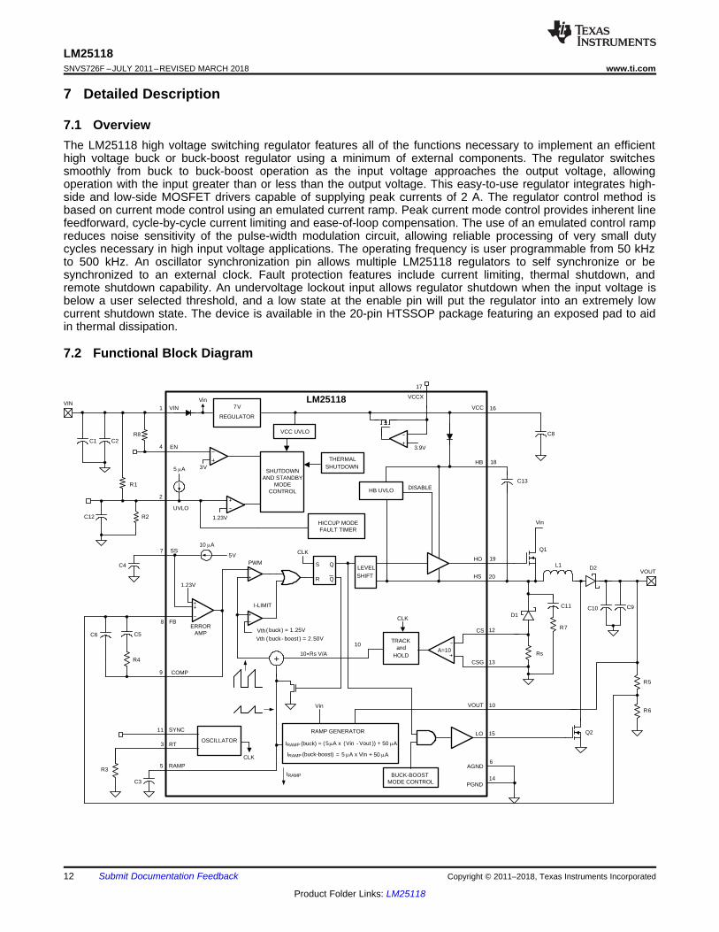
7.1 OverviewThe LM25118 high voltage switching regulator features all of the functions necessary to implement an efficienthigh voltage buck or buck-boost regulator using a minimum of external components. The regulator switchessmoothly from buck to buck-boost operation as the input voltage approaches the output voltage, allowingoperation with the input greater than or less than the output voltage. This easy-to-use regulator integrates high-side and low-side MOSFET drivers capable of supplying peak currents of 2 A. The regulator control method isbased on current mode control using an emulated current ramp. Peak current mode control provides inherent linefeedforward, cycle-by-cycle current limiting and ease-of-loop compensation. The use of an emulated control rampreduces noise sensitivity of the pulse-width modulation circuit, allowing reliable processing of very small dutycycles necessary in high input voltage applications. The operating frequency is user programmable from 50 kHzto 500 kHz. An oscillator synchronization pin allows multiple LM25118 regulators to self synchronize or besynchronized to an external clock. Fault protection features include current limiting, thermal shutdown, andremote shutdown capability. An undervoltage lockout input allows regulator shutdown when the input voltage isbelow a user selected threshold, and a low state at the enable pin will put the regulator into an extremely lowcurrent shutdown state. The device is available in the 20-pin HTSSOP package featuring an exposed pad to aidin thermal dissipation.
7.2 Functional Block Diagram

HB
VOUT
CSG
CS
LO
HO
HS
LM25118
VIN
D1
Q2 (OFF)
D2
Q1
Buck Switch Current
DiodeCurrent
13
LM25118www.ti.com SNVS726F –JULY 2011–REVISED MARCH 2018
Product Folder Links: LM25118
Submit Documentation FeedbackCopyright © 2011–2018, Texas Instruments Incorporated
7.3 Feature DescriptionA buck-boost regulator can maintain regulation for input voltages either higher or lower than the output voltage.The challenge is that buck-boost power converters are not as efficient as buck regulators. The LM25118 hasbeen designed as a dual-mode controller whereby the power converter acts as a buck regulator while the inputvoltage is above the output. As the input voltage approaches the output voltage, a gradual transition to the buck-boost mode occurs. The dual mode approach maintains regulation over a wide range of input voltages, whilemaintaining the optimal conversion efficiency in the normal buck mode. The gradual transition between modeseliminates disturbances at the output during transitions. Figure 8 shows the basic operation of the LM25118regulator in the buck mode. In buck mode, transistor Q1 is active and Q2 is disabled. The inductor current rampsin proportion to the Vin – Vout voltage difference when Q1 is active and ramps down through the recirculatingdiode D1 when Q1 is off. The first order buck mode transfer function is VOUT/VIN = D, where D is the duty cycleof the buck switch, Q1.
Figure 8. Buck Mode Operation

18 17 16 15 14 13 120
10
20
30
40
50
60
70
80
90
100D
UT
Y C
YC
LE (
%)
VIN (V)
HB
VOUT
CSG
CS
LO
HO
HS
LM25118D1
Q2
D2
Q1
Buck Switch Current
DiodeCurrent
VIN
14
LM25118SNVS726F –JULY 2011–REVISED MARCH 2018 www.ti.com
Product Folder Links: LM25118
Submit Documentation Feedback Copyright © 2011–2018, Texas Instruments Incorporated
Feature Description (continued)Figure 9 shows the basic operation of buck-boost mode. In buck-boost mode, both Q1 and Q2 are active for thesame time interval each cycle. The inductor current ramps up (proportional to VIN) when Q1 and Q2 are activeand ramps down through the recirculating diode during the off-time. The first order buck-boost transfer function isVOUT/VIN = D/(1 – D), where D is the duty cycle of Q1 and Q2.
Figure 9. Buck-Boost Mode Operation
Figure 10. Mode Dependence on Duty Cycle (VOUT =12 V)
SYNC
LM25118
SYNC
LM25118
UP TO FIVE LM25118 DEVICES
RT =6.4 x 10⁹
f- 3.02 x 10³
15
LM25118www.ti.com SNVS726F –JULY 2011–REVISED MARCH 2018
Product Folder Links: LM25118
Submit Documentation FeedbackCopyright © 2011–2018, Texas Instruments Incorporated
Feature Description (continued)7.3.1 UVLOAn undervoltage lockout pin is provided to disable the regulator when the input is below the desired operatingrange. If the UVLO pin is below 1.13 V, the regulator enters a standby mode with the outputs disabled, but withVCC regulator operating. If the UVLO input exceeds 1.23 V, the regulator will resume normal operation. Avoltage divider from the input to ground can be used to set a VIN threshold to disable the regulator in brownoutconditions or for low input faults.
If a current limit fault exists for more than 256 clock cycles, the regulator will enter a hiccup mode of currentlimiting and the UVLO pin will be pulled low by an internal switch. This switch turns off when the UVLO pinapproaches ground potential allowing the UVLO pin to rise. A capacitor connected to the UVLO pin will delay thereturn to a normal operating level and thereby set the off-time of the hiccup mode fault protection. An internal 5-µA pullup current pulls the UVLO pin to a high state to ensure normal operation when the VIN UVLO function isnot required and the pin is left floating.
7.3.2 Oscillator and Sync CapabilityThe LM25118 oscillator frequency is set by a single external resistor connected between the RT pin and theAGND pin. The RT resistor should be located very close to the device and connected directly to the pins of theIC. To set a desired oscillator frequency (f), the necessary value for the RT resistor can be calculated fromEquation 1:
(1)
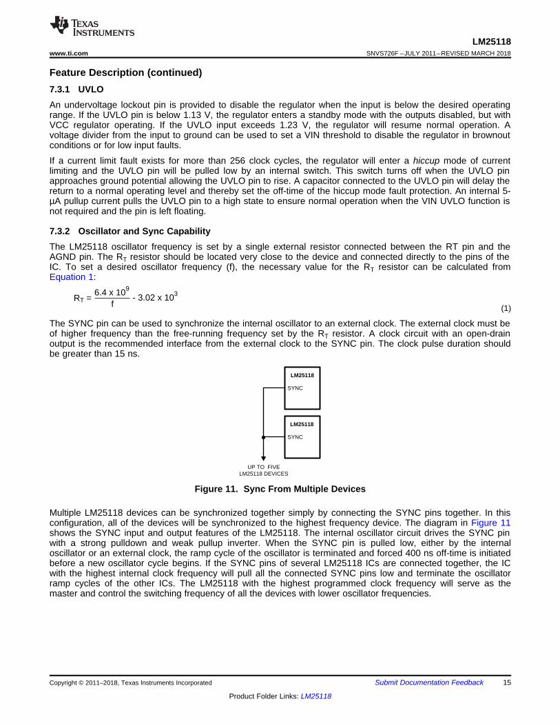
The SYNC pin can be used to synchronize the internal oscillator to an external clock. The external clock must beof higher frequency than the free-running frequency set by the RT resistor. A clock circuit with an open-drainoutput is the recommended interface from the external clock to the SYNC pin. The clock pulse duration shouldbe greater than 15 ns.
Figure 11. Sync From Multiple Devices
Multiple LM25118 devices can be synchronized together simply by connecting the SYNC pins together. In thisconfiguration, all of the devices will be synchronized to the highest frequency device. The diagram in Figure 11shows the SYNC input and output features of the LM25118. The internal oscillator circuit drives the SYNC pinwith a strong pulldown and weak pullup inverter. When the SYNC pin is pulled low, either by the internaloscillator or an external clock, the ramp cycle of the oscillator is terminated and forced 400 ns off-time is initiatedbefore a new oscillator cycle begins. If the SYNC pins of several LM25118 ICs are connected together, the ICwith the highest internal clock frequency will pull all the connected SYNC pins low and terminate the oscillatorramp cycles of the other ICs. The LM25118 with the highest programmed clock frequency will serve as themaster and control the switching frequency of all the devices with lower oscillator frequencies.

Emulated Ramp
Ton
Buck:
Buck - Boost:
t
v
Pedestal Level = (volts/amp)Rsx10
CRAMP
tONx)PA50+)- VOUTVIN(xPA5(
CRAMP
tONx)PA50+VINxPA5(
SYNC
100 PA
S
R
Q
Q
DEADTIME ONE - SHOT
1.23V
I 1/RT
16
LM25118SNVS726F –JULY 2011–REVISED MARCH 2018 www.ti.com
Product Folder Links: LM25118
Submit Documentation Feedback Copyright © 2011–2018, Texas Instruments Incorporated
Feature Description (continued)
Figure 12. Simplified Oscillator and Block Diagram With Sync I/O Circuit
7.3.3 Error Amplifier and PWM ComparatorThe internal high gain error amplifier generates an error signal proportional to the difference between theregulated output voltage and an internal precision reference (1.23 V). The output of the error amplifier isconnected to the COMP pin. Loop compensation components, typically a type II network shown in Figure 18 areconnected between the COMP and FB pins. This network creates a low-frequency pole, a zero, and a noisereducing high-frequency pole. The PWM comparator compares the emulated current sense signal from theRAMP generator to the error amplifier output voltage at the COMP pin. The same error amplifier is used foroperation in buck and buck-boost mode.
Figure 13. Composition of Emulated Current Signal

gm x L
CRAMPRS x A =
gm x LCRAMP =
A x RS
5 PAV
x VIN + 50 PAIRAMP (buck - boost) =
5 PAV
x (VIN - VOUT) + 50 PAIRAMP (buck) =
17
LM25118www.ti.com SNVS726F –JULY 2011–REVISED MARCH 2018
Product Folder Links: LM25118
Submit Documentation FeedbackCopyright © 2011–2018, Texas Instruments Incorporated
Feature Description (continued)7.3.4 Ramp GeneratorThe ramp signal of a pulse-width modulator with current mode control is typically derived directly from the buckswitch drain current. This switch current corresponds to the positive slope portion of the inductor current signal.Using this signal for the PWM ramp simplifies the control loop transfer function to a single pole response andprovides inherent input voltage feed-forward compensation. The disadvantage of using the buck switch currentsignal for PWM control is the large leading edge spike due to circuit parasitics. The leading edge spike must befiltered or blanked to avoid early termination of the PWM pulse. Also, the current measurement may introducesignificant propagation delays. The filtering, blanking time, and propagation delay limit the minimal achievablepulse width. In applications where the input voltage may be relatively large in comparison to the output voltage,controlling a small pulse width is necessary for regulation. The LM25118 uses a unique ramp generator whichdoes not actually measure the buck switch current but instead creates a signal representing or emulating theinductor current. The emulated ramp provides signal to the PWM comparator that is free of leading edge spikesand measurement or filtering delays. The current reconstruction is comprised of two elements: a sample-and-hold pedestal level and a ramp capacitor that is charged by a controlled current source. See Figure 13 for details.
The sample-and-hold pedestal level is derived from a measurement of the recirculating current through a currentsense resistor in series with the recirculating diode of the buck regulator stage. A small value current-sensingresistor is required between the recirculating diode anode and ground. The CS and CSG pins should be Kelvinconnected directly to the sense resistor. The voltage level across the sense resistor is sampled and held justprior to the onset of the next conduction interval of the buck switch. The current sensing and sample-and-holdprovide the DC level of the reconstructed current signal. The sample and hold of the recirculating diode current isvalid for both buck and buck-boost modes. The positive slope inductor current ramp is emulated by an externalcapacitor connected from the RAMP pin to the AGND and an internal voltage controlled current source. In buckmode, the ramp current source that emulates the inductor current is a function of the VIN and VOUT voltages perEquation 2.
(2)
In buck-boost mode, the ramp current source is a function of the input voltage VIN, per Equation 3.
(3)
Proper selection of the RAMP capacitor (CRAMP) depends upon the value of the output inductor (L) and thecurrent sense resistor (RS). For proper current emulation, the sample and hold pedestal value and the rampamplitude must have the same relative relationship to the actual inductor current. That is:
where• gm is the ramp generator transconductance (5 µA/V)• A is the current sense amplifier gain (10 V/V) (4)
The ramp capacitor should be located very close to the device and connected directly to the RAMP and AGNDpins.

1 +VOUT
Iout xVIN
A =10k
1k + RG
18
LM25118SNVS726F –JULY 2011–REVISED MARCH 2018 www.ti.com
Product Folder Links: LM25118
Submit Documentation Feedback Copyright © 2011–2018, Texas Instruments Incorporated
Feature Description (continued)The relationship between the average inductor current and the pedestal value of the sampled inductor currentcan cause instability in certain operating conditions. This instability is known as sub-harmonic oscillation, whichoccurs when the inductor ripple current does not return to its initial value by the start of the next switching cycle.Sub-harmonic oscillation is normally characterized by observing alternating wide and narrow pulses at the switchnode. Adding a fixed slope voltage ramp (slope compensation) to the current sense signal prevents thisoscillation. The 50 µA of offset current provided from the emulated current source adds enough slopecompensation to the ramp signal for output voltages less than or equal to 12 V. For higher output voltages,additional slope compensation may be required. In such applications, the ramp capacitor can be decreased fromthe nominal calculated value to increase the ramp slope compensation.
The pedestal current sample is obtained from the current sense resistor (Rs) connected to the CS and CSG pins.It is sometimes helpful to adjust the internal current sense amplifier gain (A) to a lower value to obtain the highercurrent limit threshold. Adding a pair of external resistors RG in a series with CS and CSG as shown in Figure 14reduces the current sense amplifier gain A according to Equation 5.
(5)
7.3.5 Current LimitIn the buck mode the average inductor current is equal to the output current (Iout). In buck-boost mode theaverage inductor current is approximately equal to:
(6)
Consequently, the inductor current in buck-boost mode is much larger especially when VOUT is large relative toVIN. The LM25118 provides a current monitoring scheme to protect the circuit from possible overcurrentconditions. When set correctly, the emulated current sense signal is proportional to the buck switch current with ascale factor determined by the current sense resistor. The emulated ramp signal is applied to the current limitcomparator. If the peak of the emulated ramp signal exceeds 1.25 V when operating in the buck mode, the PWMcycle is immediately terminated (cycle-by-cycle current limiting). In buck-boost mode the current limit threshold isincreased to 2.50 V to allow higher peak inductor current. To further protect the external switches duringprolonged overload conditions, an internal counter detects consecutive cycles of current limiting. If the counterdetects 256 consecutive current limited PWM cycles, the LM25118 enters a low power dissipation hiccup mode.In the hiccup mode, the output drivers are disabled, the UVLO pin is momentarily pulled low, and the soft-startcapacitor is discharged. The regulator is restarted with a normal soft-start sequence once the UVLO pin chargesback to 1.23 V. The hiccup mode off-time can be programmed by an external capacitor connected from UVLOpin to ground. This hiccup cycle will repeat until the output overload condition is removed.

0 100 200 300 400 500 600
FREQUENCY (kHz)
0.75
0.8
0.85
0.9
0.95
1
MA
X D
UT
Y C
YC
LE
CSG
CS
IL
TRACK and HOLD
RG
RAMP
1k RG
1k
RS+
-
10k
10k0.2V
+
-
RAMPRESET
Vth
CRAMP
CURRENT LIMITCOMPARATOR
IRAMP
CURRENT SENSEAMPLIFIER
19
LM25118www.ti.com SNVS726F –JULY 2011–REVISED MARCH 2018
Product Folder Links: LM25118
Submit Documentation FeedbackCopyright © 2011–2018, Texas Instruments Incorporated
Feature Description (continued)In applications with low output inductance and high input voltage, the switch current may overshoot due to thepropagation delay of the current limit comparator and control circuitry. If an overshoot should occur, the sample-and-hold circuit will detect the excess recirculating diode current. If the sample-and-hold pedestal level exceedsthe internal current limit threshold, the buck switch will be disabled and will skip PWM cycles until the inductorcurrent has decayed below the current limit threshold. This approach prevents current runaway conditions due topropagation delays or inductor saturation since the inductor current is forced to decay before the buck switch isturned on again.
Figure 14. Current Limit and Ramp Circuit
7.3.6 Maximum Duty CycleEach conduction cycle of the buck switch is followed by a forced minimum off-time of 400 ns to allow sufficienttime for the recirculating diode current to be sampled. This forced off-time limits the maximum duty cycle of thecontroller. The actual maximum duty cycle will vary with the operating frequency of Equation 7.
DMAX = 1 - f × 400 × 10–9
where• f is the oscillator frequency in Hz (7)
Figure 15. Maximum Duty Cycle vs Frequency

VoutD =
Vin + Vout
20
LM25118SNVS726F –JULY 2011–REVISED MARCH 2018 www.ti.com
Product Folder Links: LM25118
Submit Documentation Feedback Copyright © 2011–2018, Texas Instruments Incorporated
Feature Description (continued)Limiting the maximum duty cycle will limit the maximum boost ratio (VOUT/VIN) while operating in buck-boostmode. For example, from Figure 15, at an operating frequency of 500 kHz, DMAX is 80%. Using the buck-boosttransfer function.
(8)
with• D = 80%, solving for VOUT results in• VOUT = 4 × VIN
With a minimum input voltage of 5 V, the maximum possible output voltage is 20 V at f = 500 kHz. The buck-boost step-up ratio can be increased by reducing the operating frequency which increases the maximum dutycycle.
7.3.7 Soft StartThe soft-start feature allows the regulator to gradually reach the initial steady-state operating point, thus reducingstart-up stresses and surges. The internal 10-µA soft-start current source gradually charges an external soft-startcapacitor connected to the SS pin. The SS pin is connected to the positive input of the internal error amplifier.The error amplifier controls the pulse-width modulator such that the FB pin approximately equals the SS pin asthe SS capacitor is charged. Once the SS pin voltage exceeds the internal 1.23-V reference voltage, the erroramp is controlled by the reference instead of the SS pin. The SS pin voltage is clamped by an internal amplifierat a level of 150 mV above the FB pin voltage. This feature provides a soft-start controlled recovery in the eventa severe overload pulls the output voltage (and FB pin) well below normal regulation but doesn’t persist for 256clock cycles.
Various sequencing and tracking schemes can be implemented using external circuits that limit or clamp thevoltage level of the SS pin. The SS pin acts as a noninverting input to the error amplifier anytime SS voltage isless than the 1.23-V reference. In the event a fault is detected (overtemperature, VCC undervoltage, hiccupcurrent limit), the soft-start capacitor will be discharged. When the fault condition is no longer present, a new soft-start sequence will begin.
7.3.8 HO OutputThe LM25118 contains a high-side, high-current gate driver and associated high voltage level shift. This gatedriver circuit works in conjunction with an internal diode and an external bootstrap capacitor. A 0.1-µF ceramiccapacitor, connected with short traces between the HB pin and HS pin is recommended for most circuitconfigurations. The size of the bootstrap capacitor depends on the gate charge of the external FET. During theoff-time of the buck switch, the HS pin voltage is approximately –0.5 V and the bootstrap capacitor is chargedfrom VCC through the internal bootstrap diode. When operating with a high PWM duty cycle, the buck switch willbe forced off each cycle for 400 ns to ensure that the bootstrap capacitor is recharged.
7.3.9 Thermal ProtectionInternal Thermal Shutdown circuitry is provided to protect the integrated circuit in the event the maximum junctiontemperature is exceeded. When activated, typically at 165°C, the controller is forced into a low power reset state,disabling the output driver and the bias regulator. This protection is provided to prevent catastrophic failures fromaccidental device overheating.

21
LM25118www.ti.com SNVS726F –JULY 2011–REVISED MARCH 2018
Product Folder Links: LM25118
Submit Documentation FeedbackCopyright © 2011–2018, Texas Instruments Incorporated
7.4 Device Functional ModesFigure 10 shows how duty cycle effects the operational mode and is useful for reference in the followingdiscussions. Initially, only the buck switch is active and the buck duty cycle increases to maintain outputregulation as VIN decreases. When VIN is approximately equal to 15.5 V, the boost switch begins to operate witha low duty cycle. If VIN continues to fall, the boost switch duty cycle increases and the buck switch duty cycledecreases until they become equal at VIN = 13.2 V.
7.4.1 Buck Mode Operation: VIN > VOUTThe LM25118 buck-boost regulator operates as a conventional buck regulator with emulated current modecontrol while VIN is greater than VOUT and the buck mode duty cycle is less than 75%. In buck mode, the LOgate drive output to the boost switch remains low.
7.4.2 Buck-Boost Mode Operation: VIN ≊≊ VOUTWhen VIN decreases relative to VOUT, the duty cycle of the buck switch will increase to maintain regulation.Once the duty cycle reaches 75%, the boost switch starts to operate with a very small duty cycle. As VIN isfurther decreased, the boost switch duty cycle increases until it is the same as the buck switch. As VIN is furtherdecreased below VOUT, the buck and boost switch operate together with the same duty cycle and the regulatoris in full buck-boost mode. This feature allows the regulator to transition smoothly from buck to buck-boost mode.Note that the regulator can be designed to operate with VIN less than 4 V, but VIN must be at least 5 V duringstart-up. Figure 16 shows a timing illustration of the gradual transition from buck to buck-boost mode when theinput voltage ramps downward over a few switching cycles.
Figure 16. Buck (HO) and Boost (LO) Switch Duty Cycle vs. Time,Illustrating Gradual Mode Change With Decreasing Input Voltage

Vcc
Vin
Internal Enable Signal
3.5V
VIN and VCC
10V7V
3.7V
22
LM25118SNVS726F –JULY 2011–REVISED MARCH 2018 www.ti.com
Product Folder Links: LM25118
Submit Documentation Feedback Copyright © 2011–2018, Texas Instruments Incorporated
Device Functional Modes (continued)7.4.3 High Voltage Start-Up RegulatorThe LM25118 contains a dual-mode, high voltage linear regulator that provides the VCC bias supply for thePWM controller and the MOSFET gate driver. The VIN input pin can be connected directly to input voltages ashigh as 42 V. For input voltages below 10 V, an internal low dropout switch connects VCC directly to VIN. In thissupply range, VCC is approximately equal to VIN. For VIN voltages greater than 10 V, the low dropout switch isdisabled and the VCC regulator is enabled to maintain VCC at approximately 7 V. A wide operating range of 4 Vto 42 V (with a startup requirement of at least 5 V) is achieved through the use of this dual-mode regulator.
The output of the VCC regulator is current limited to 35 mA, typical. Upon power up, the regulator sourcescurrent into the capacitor connected to the VCC pin. When the voltage at the VCC pin exceeds the VCC under-voltage threshold of 3.7 V and the UVLO input pin voltage is greater than 1.23 V, the gate driver outputs areenabled and a soft-start sequence begins. The gate driver outputs remain enabled until VCC falls below 3.5 V orthe voltage at the UVLO pin falls below 1.13 V.
In many applications, the regulated output voltage or an auxiliary supply voltage can be applied to the VCCX pinto reduce the IC power dissipation. For output voltages between 4 V and 15 V, VOUT can be connected directlyto VCCX. When the voltage at the VCCX pin is greater than 3.85 V, the internal VCC regulator is disabled andan internal switch connects VCCX to VCC, reducing the internal power dissipation.
In high voltage applications, take extra care to ensure the VIN pin voltage does not exceed the absolutemaximum voltage rating of 45 V. During line or load transients, voltage ringing on the VIN line that exceeds theabsolute maximum rating can damage the IC. Both careful PCB layout and the use of quality bypass capacitorslocated close to the VIN and GND pins are essential.
Figure 17. VIN and VCC Sequencing
7.4.4 EnableThe LM25118 contains an enable function which provides a very low input current shutdown mode. If the EN pinis pulled below 0.5 V, the regulator enters shutdown mode, drawing less than 10 µA from the VIN pin. Raisingthe EN input above 3 V returns the regulator to normal operation. The EN pin can be tied directly to the VIN pin ifthis function is not needed. It must not be left floating. A 1-MΩ pullup resistor to VIN can be used to interface withan open-collector or open-drain control signal.

(8) FB
VIN (1) (16) VCC
RT (3)
(18) HB
VOUT
AGND (6)
PGND (14)
DAP (EP)
(13) CSG
RAMP (5)
SS (7)
(12) CS
(15) LO
(10) VOUT
(19) HO
(20) HS
(9) COMP
LM25118MH
VIN
EN (4)
SYNC (11)
VCCX (17)
UVLO (2)
ON
OFF
VEN(ON)
VEN(OFF)0V
23
LM25118www.ti.com SNVS726F –JULY 2011–REVISED MARCH 2018
Product Folder Links: LM25118
Submit Documentation FeedbackCopyright © 2011–2018, Texas Instruments Incorporated
8 Application and Implementation
NOTEInformation in the following applications sections is not part of the TI componentspecification, and TI does not warrant its accuracy or completeness. TI’s customers areresponsible for determining suitability of components for their purposes. Customers shouldvalidate and test their design implementation to confirm system functionality.
8.1 Application InformationThe LM25118 high voltage switching regulator features all of the functions necessary to implement an efficienthigh voltage buck or buck-boost regulator using a minimum of external components. A buckboost regulator canmaintain regulation for input voltages either higher or lower than the output voltage.
8.2 Typical Application
Figure 18. Typical Application Circuit

24
LM25118SNVS726F –JULY 2011–REVISED MARCH 2018 www.ti.com
Product Folder Links: LM25118
Submit Documentation Feedback Copyright © 2011–2018, Texas Instruments Incorporated
Typical Application (continued)
Figure 19. 12-V, 3-A Typical Application Schematic
8.2.1 Design RequirementsThe procedure for calculating the external components is illustrated with the following design example. Thedesignations used in the design example correlate to the Figure 19. The design specifications are:• VOUT = 12 V• VIN = 5 V to 42 V• f = 300 kHz• Minimum load current (CCM operation) = 600 mA• Maximum load current = 3 A

Iripple
Ipk+
Io Buck
Ipk-
Iripple
1/Fs
L1 C
urre
nt Io/(1-D) B-B
RT =6.4 x 10⁹
f- 3.02 x 10³
25
LM25118www.ti.com SNVS726F –JULY 2011–REVISED MARCH 2018
Product Folder Links: LM25118
Submit Documentation FeedbackCopyright © 2011–2018, Texas Instruments Incorporated
Typical Application (continued)8.2.2 Detailed Design Procedure
8.2.2.1 Custom Design With WEBENCH® ToolsClick here to create a custom design using the LM25118 device with the WEBENCH® Power Designer.1. Start by entering the input voltage (VIN), output voltage (VOUT), and output current (IOUT) requirements.2. Optimize the design for key parameters such as efficiency, footprint, and cost using the optimizer dial.3. Compare the generated design with other possible solutions from Texas Instruments.
The WEBENCH Power Designer provides a customized schematic along with a list of materials with real-timepricing and component availability.
In most cases, these actions are available:• Run electrical simulations to see important waveforms and circuit performance• Run thermal simulations to understand board thermal performance• Export customized schematic and layout into popular CAD formats• Print PDF reports for the design, and share the design with colleagues
Get more information about WEBENCH tools at www.ti.com/WEBENCH.
8.2.2.2 R7 = RT
RT sets the oscillator switching frequency. Generally speaking, higher operating frequency applications will usesmaller components, but have higher switching losses. An operating frequency of 300 kHz was selected for thisexample as a reasonable compromise for both component size and efficiency. The value of RT can be calculatedas:
(9)
therefore, R7 = 18.3 kΩ
Figure 20. Inductor Current Waveform

OUT OUT IN(MIN) RIPPLE(BUCK-BOOST)2(PEAK)
IN(MIN) TOL
I (V V ) II
V 2(1 L )
Ku
RIPPLE(BUCK)OUT1(PEAK)
TOL
III
2(1 L )
K
IN(MIN) OUT
OUT IN(MIN) RIPPLE
V (V )L1 Buck-Boost Mode
(V V ) f I
u u
OUT IN(MAX) OUT
IN(MAX) RIPPLE
V (V V )L1 Buck Mode
V f I
u u
26
LM25118SNVS726F –JULY 2011–REVISED MARCH 2018 www.ti.com
Product Folder Links: LM25118
Submit Documentation Feedback Copyright © 2011–2018, Texas Instruments Incorporated
Typical Application (continued)8.2.2.3 Inductor Selection – L1The inductor value is determined based upon the operating frequency, load current, ripple current, and the inputand output voltages. See Figure 20 for details.
To keep the circuit in continuous conduction mode (CCM), the maximum ripple current IRIPPLE should be lessthan twice the minimum load current. For the specified minimum load of 0.6 A, the maximum ripple current is 1.2Ap-p. Also, the minimum value of L must be calculated both for a buck and buck-boost configurations. The finalvalue of inductance will generally be a compromise between the two modes. It is desirable to have a larger valueinductor for buck mode, but the saturation current rating for the inductor must be large for buck-boost mode,resulting in a physically large inductor. Additionally, large value inductors present buck-boost mode loopcompensation challenges which will be discussed in Error Amplifier Configuration . For the design example, theinductor values in both modes are calculated as:
(10)
where• VOUT is the output voltage• VIN(MAX) is the maximum input voltage• f is the switching frequency• IRIPPLE is the selected inductor peak to peak ripple current (1.2 A selected for this example)• VIN(MIN) is the minimum input voltage• (11)
The resulting inductor values are:L1 = 23.8 µH, Buck Mode (12)L1 = 9.8 µH, Buck-Boost mode (13)
A 10-µH inductor was selected which is a compromise between these values, while favoring the buck-boostmode. As illustrated in the compensation section, the inductor value should be as low as possible to move thebuck-boost right-half-plane zero to a higher frequency. The ripple current is then rechecked with the selectedinductor value using Equation 10 and Equation 11.
IRIPPLE(BUCK) = 2.86 A (14)IRIPPLE(BUCK-BOOST) = 1.17 A (15)
Because the inductor selected is lower than calculated for the Buck mode, the minimum load current for CCM inbuck mode is 1.42 A at maximum VIN.
With a 10-µH inductor, the worst case peak inductor currents can be estimated for each case, assuming a 20%inductor value tolerance and 80% efficiency of the converter.
(16)
where• η is efficiency• LTOL is the inductor tolerance (17)

C15 = CRAMP =L x 10-6
2 x RSENSE
(BUCK-BOOST)IN(MIN) OUT RIPPLE(BUCK-BOOST)OUT
BUCK-BOOSTIN(MIN)
2.5 (1 M)R13
V V II10 K
V 2
§ · ¨ ¸¨ ¸K© ¹
(BUCK)RIPPLE(BUCK)OUT
BUCK
1.25(1 M)R13
II10 K
2
§ · ¨ ¸
K© ¹
BUCK BOOSTIN(MIN)
10K 1
Vt
BUCKIN(MAX) OUT
10K 1
V Vt
27
LM25118www.ti.com SNVS726F –JULY 2011–REVISED MARCH 2018
Product Folder Links: LM25118
Submit Documentation FeedbackCopyright © 2011–2018, Texas Instruments Incorporated
Typical Application (continued)For this example, Equation 16 and Equation 17 yield:
I1(PEAK) = 5.33 A (18)I2(PEAK) = 13.4 A (19)
An acceptable current limit setting would be 6.7 A for buck mode because the LM25118 automatically doublesthe current limit threshold in buck-boost mode. The selected inductor must have a saturation current rating atleast as high as the buck-boost mode cycle-by-cycle current limit threshold, in this case at least 13.5 A. A 10-µH,15-A inductor was chosen for this application.
8.2.2.4 R13 = RSENSE
To select the current sense resistor, begin by calculating the minimum K values for each mode usingEquation 20 and Equation 21. K represents the slope compensation of the controller and is different for eachmode, KBUCK and KBUCK-BOOST. KBUCK and KBUCK-BOOST were selected to be 1.33 and 3, respectively.
(20)
(21)KBUCK = 1.33 (22)KBUCK-BOOST = 3 (23)
Use Equation 24 and Equation 25 to calculate RSENSE for each mode of operation. A design margin, M, should beselected between 10%-30% to allow for component tolerances. For this design M was selected to be 10%.
(24)
(25)R13(BUCK) = 19.89 mΩ (26)R13(BUCK-BOOST) = 15.5 mΩ (27)
An RSENSE value of no more than 15.5 mΩ must be used to ensure the required maximum output current in thebuck-boost mode. A standard value of 15 mΩ was selected for this design.
8.2.2.5 C15 = CRAMP
With the inductor value selected, the value of C3 necessary for the emulation ramp circuit is:
(28)
With the inductance value (L1) selected as 10 µH, the calculated value for CRAMP is 333 pF. A standard value of330 pF was selected.

OUTMAX
OUT IN(MIN) RIPPLE(BUCK-BOOST)OUT
IN(MIN)
VESR
V V II
V 2
'
OUT MAX OUTMIN MAX
OUT IN(MIN) OUT
I D VC With D
f V V V
u
u '
6OUT
IN(MIN) OUTLIMIT(BUCK-BOOST)
50 10 V2.5
C15 f (V V )I
10 R13
u u
u u
u
6OUT
IN(MAX)LIMIT(BUCK)
50 10 V1.25
C15 f VI
10 R13
u u
u u
u
28
LM25118SNVS726F –JULY 2011–REVISED MARCH 2018 www.ti.com
Product Folder Links: LM25118
Submit Documentation Feedback Copyright © 2011–2018, Texas Instruments Incorporated
Typical Application (continued)8.2.2.6 Inductor Current Limit CalculationThe current limit for each mode can be calculated using Equation 29 and Equation 31. If the peak current limit isless than the calculated inductor peak current, the R13 and C15 need to be recalculated. This can be done byincreasing the previous K values or M and reiterating the calculations.
(29)ILIMIT (BUCK) = 7.37 A (30)
(31)ILIMIT (BUCK-BOOST) = 14.29 A (32)
8.2.2.7 C9 - C12 = Output CapacitorsIn buck-boost mode, the output capacitors C9 – C12 must supply the entire output current during the switch on-time. For this reason, the output capacitors are chosen for operation in buck-boost mode, the demands beingmuch less in buck operation. Both bulk capacitance and ESR must be considered to ensure a given output ripplevoltage. Buck-boost mode capacitance can be estimated from:
(33)
ESR requirements can be estimated from:
(34)
For this example, with a ΔVOUT (output ripple) of 50 mV:CMIN = 141 µF (35)ESRMAX = 4.6 mΩ (36)
If hold-up times are a consideration, the values of input and output capacitors must be increased appropriately.Note that it is usually advantageous to use multiple capacitors in parallel to achieve the ESR value required.Also, it is good practice to put a 0.1-µF to 0.47-µF ceramic capacitor directly on the output pins of the supply toreduce high-frequency noise. Ceramic capacitors have good ESR characteristics, and are a good choice for inputand output capacitors. Note that the effective capacitance of ceramic capacitors decreases with DC bias. Forlarger bulk values of capacitance, a low-ESR electrolytic is usually used. However, electrolytic capacitors havepoor tolerance, especially over temperature, and the selected value should be selected larger than the calculatedvalue to allow for temperature variation. Allowing for component tolerances, the following values of Cout werechosen for this design example:
Two 180-µF Oscon electrolytic capacitors for bulk capacitance
Two 47-µF ceramic capacitors to reduce ESR
Two 0.47-µF ceramic capacitors to reduce spikes at the output
8.2.2.8 D1Reverse recovery currents degrade performance and decrease efficiency. For these reasons, a Schottky diode ofappropriate ratings should be used for D1. The voltage rating of the boost diode should be equal to VOUT plussome margin.
IRMS(BUCK-BOOST) =1 - D
IOUT D(1 -D)
IRMS(BUCK) = IOUT D(1 -D)
29
LM25118www.ti.com SNVS726F –JULY 2011–REVISED MARCH 2018
Product Folder Links: LM25118
Submit Documentation FeedbackCopyright © 2011–2018, Texas Instruments Incorporated
Typical Application (continued)8.2.2.9 D4A Schottky type recirculating diode is required for all LM25118 applications. The near ideal reverse recoverycharacteristics and low forward voltage drop are particularly important diode characteristics for high input voltageand low output voltage applications. The reverse recovery characteristic determines how long the current surgelasts each cycle when the buck switch is turned on. The reverse recovery characteristics of Schottky diodesminimize the peak instantaneous power in the buck switch during the turn-on transition. The reverse breakdownrating of the diode should be selected for the maximum VIN plus some safety margin.
The forward voltage drop has a significant impact on the conversion efficiency, especially for applications with alow output voltage. Rated current for diodes vary widely from various manufacturers. For the LM25118 thiscurrent is user selectable through the current sense resistor value. Assuming a worst-case, 0.6-V drop across thediode, the maximum diode power dissipation can be high. The diode should have a voltage rating of VIN and acurrent rating of IOUT. A conservative design would at least double the advertised diode rating becausespecifications between manufacturers vary. For the reference design, a 100-V, 10-A Schottky in a D2PAKpackage was selected.
8.2.2.10 C1 – C5 = Input CapacitorsA typical regulator supply voltage has a large source impedance at the switching frequency. Good-quality inputcapacitors are necessary to limit the ripple voltage at the VIN pin while supplying most of the switch currentduring the buck switch on-time. When the buck switch turns on, the current into the buck switch steps from zeroto the lower peak of the inductor current waveform, then ramps up to the peak value, and then drops to the zeroat turnoff. The RMS current rating of the input capacitors depends on which mode of operation is most critical.
(37)
The RMS current demand on the input capacitor(s) is at the maximum value when the duty cycle is at 50%.
(38)
Checking both modes of operation we find:IRMS(BUCK) = 1.5 A (39)IRMS(BUCK-BOOST) = 4.7 A (40)
Therefore C1 — C5 should be sized to handle 4.7 A of ripple current. Quality ceramic capacitors with a low ESRshould be selected. To allow for capacitor tolerances, five 2.2-µF, 100-V ceramic capacitors will be used. If stepinput voltage transients are expected near the maximum rating of the LM25118, a careful evaluation of theringing and possible spikes at the device VIN pin should be completed. An additional damping network or inputvoltage clamp may be required in these cases.
8.2.2.11 C20The capacitor at the VCC pin provides noise filtering and stability for the VCC regulator. The recommended valueof C20 should be no smaller than 0.1 µF, and should be a good-quality, low-ESR, ceramic capacitor. A value of 1µF was selected for this design. C20 should be 10 x C8.
If operating without VCCX, thenfOSC x (QCBuck + Boost) + ILOAD(INTERNAL) (41)
must be less than the VCC current limit.
8.2.2.12 C8The bootstrap capacitor between the HB and HS pins supplies the gate current to charge the buck switch gate atturnon. The recommended value of C8 is 0.1 µF to 0.47 µF, and should be a good-quality, low-ESR, ceramiccapacitor. A value of 0.1 µF was chosen for this design.
OFFIN
C21 R1 R3 R1 R3t Ln 1 .98
R1 R3 V R3
ª º « »
¬ ¼
R3 = 1.23 xVIN(MIN) + 5 PA x R1 - 1.23
R1
- 1R9R8
1.23V
VOUT=
tSS =10 PA
C16 x 1.23V
30
LM25118SNVS726F –JULY 2011–REVISED MARCH 2018 www.ti.com
Product Folder Links: LM25118
Submit Documentation Feedback Copyright © 2011–2018, Texas Instruments Incorporated
Typical Application (continued)8.2.2.13 C16 = CSS
The capacitor at the SS pin determines the soft-start time, that is, the time for the reference voltage and theoutput voltage, to reach the final regulated value. The time is determined from:
(42)
and assumes a current limit>Iload + ICout
For this application, a C16 value of 0.1 µF was chosen which corresponds to a soft-start time of about 12 ms.
8.2.2.14 R8, R9R8 and R9 set the output voltage level, the ratio of these resistors is calculated from:
(43)
For a 12-V output, the R8/R9 ratio calculates to 8.76. The resistors should be chosen from standard valueresistors and a good starting point is to select resistors within power ratings appropriate for the output voltage.Values of 309 Ω for R9 and 2.67 kΩ for R8 were selected.
8.2.2.15 R1, R3, C21A voltage divider can be connected to the UVLO pin to set a minimum operating voltage VIN(UVLO) for theregulator. If this feature is required, the easiest approach to select the divider resistor values is to choose a valuefor R1 between 10 kΩ and 100 kΩ, while observing the minimum value of R1 necessary to allow the UVLOswitch to pull the UVLO pin low. This value is:
R1 ≥ 1000 × VIN(MAX)
R1 ≥ 75 k
R3 is then calculated from:
(44)
Because VIN(MIN) for our example is 5 V, set VIN(UVLO) to 4 V for some margin in component tolerances and inputripple.
R1 = 75 k is chosen because it is a standard value
R3 = 29.332 k is calculated from Equation 44. 29.4 k was used because it is a standard value
Capacitor C21 provides filtering for the divider and the off time of the hiccup duty cycle during current limit. Thevoltage at the UVLO pin should never exceed 15 V when using an external set-point divider. It may be necessaryto clamp the UVLO pin at high input voltages.
Knowing the desired off time during hiccup current limit, the value of C21 is given by:
(45)
Notice that tOFF varies with VIN
In this example, C21 was chosen to be 0.1 µF. This will set the tOFF time to 723 µs with VIN = 12 V.
8.2.2.16 R2A 1-M pullup resistor connected from the EN pin to the VIN pin is sufficient to keep enable in a high state if on-offcontrol is not used.

fz =2 x S x R4 x C18
1
ESRzero =2S x ESR x COUT
1
fRHPzero =RLOAD (1 - D)2
2S x L x D
MAXP(MOD)
LOAD OUT
1 Df
2 R C
Su u
DCGain(MOD) =RLOAD x VIN
10RS(VIN + 2VOUT)
31
LM25118www.ti.com SNVS726F –JULY 2011–REVISED MARCH 2018
Product Folder Links: LM25118
Submit Documentation FeedbackCopyright © 2011–2018, Texas Instruments Incorporated
Typical Application (continued)8.2.2.17 SnubberA snubber network across the buck recirculating diode reduces ringing and spikes at the switching node.Excessive ringing and spikes can cause erratic operation and increase noise at the regulator output. In the limit,spikes beyond the maximum voltage rating of the LM25118 or the recirculating diode can damage these devices.Selecting the values for the snubber is best accomplished through empirical methods. First, make sure the leadlengths for the snubber connections are very short. Start with a resistor value between 5 and 20 Ω. Increasingthe value of the snubber capacitor results in more damping, however the snubber losses increase. Select aminimum value of the capacitor that provides adequate clamping of the diode waveform at maximum load. Asnubber may be required for the boost diode as well. The same empirical procedure applies. Snubbers were notnecessary in this example.
8.2.2.18 Error Amplifier Configuration
8.2.2.18.1 R4, C18, C17
These components configure the error amplifier gain characteristics to accomplish a stable overall loop gain. Oneadvantage of current mode control is the ability to close the loop with only three feedback components, R4, C18,and C17. The overall loop gain is the product of the modulator gain and the error amplifier gain. The DCmodulator gain of the LM25118 is as follows:
(46)
The dominant, low frequency pole of the modulator is determined by the load resistance (RLOAD) and outputcapacitance (COUT). The corner frequency of this pole is:
(47)
For this example, RLOAD = 4 Ω, DMAX = 0.705, and COUT = 454 µF, therefore:fP(MOD) = 149 Hz (48)
DC Gain(MOD) = 4.59 = 13.25 dB (49)
Additionally, there is a right-half plane (RHP) zero associated with the modulator. The frequency of the RHP zerois:
(50)fRHPzero = 7.8 kHz (51)
The output capacitor ESR produces a zero given by:
(52)ESRZERO = 76 kHz (53)
The RHP zero complicates compensation. The best design approach is to reduce the loop gain to cross zero atabout 25% of the calculated RHP zero frequency. The Type ll error amplifier compensation provided by R4, C18,and C17 places one pole at the origin for high DC gain. The second pole should be placed close to the RHPzero. The error amplifier zero (Equation 54) should be placed near the dominate modulator pole. This is a goodstarting point for compensation.
Components R4 and C18 configure the error amplifier as a Type II configuration which has a DC pole and a zeroat
(54)
32
LM25118SNVS726F –JULY 2011–REVISED MARCH 2018 www.ti.com
Product Folder Links: LM25118
Submit Documentation Feedback Copyright © 2011–2018, Texas Instruments Incorporated
Typical Application (continued)C17 introduces an additional pole used to cancel high frequency switching noise. The error amplifier zerocancels the modulator pole leaving a single pose response at the crossover frequency of the loop gain if thecrossover frequency is much lower than the right half plane zero frequency. A single pole response at thecrossover frequency yields a very stable loop with 90 degrees of phase margin.
For the design example, a target loop bandwidth (crossover frequency) of 2.0 kHz was selected (about 25% ofthe right-half-plane zero frequency). The error amplifier zero (fz) should be selected at a frequency near that ofthe modulator pole and much less than the target crossover frequency. This constrains the product of R4 andC18 for a desired compensation network zero to be less than 2 kHz. Increasing R4, while proportionallydecreasing C18 increases the error amp gain. Conversely, decreasing R4 while proportionally increasing C18decreases the error amp gain. For the design example C18 was selected for 100 nF and R4 was selected to be10 kΩ. These values set the compensation network zero at 159 Hz. The overall loop gain can be predicted asthe sum (in dB) of the modulator gain and the error amp gain.
If a network analyzer is available, the modulator gain can be measured and the error amplifier gain can beconfigured for the desired loop transfer function. If a network analyzer is not available, the error amplifiercompensation components can be designed with the guidelines given. Step load transient tests can beperformed to verify acceptable performance. The step load goal is minimal overshoot with a damped response.
Please see the plots shown in Figure 21 through Figure 26 which illustrate the gain and phase diagrams of thedesign example.

33
LM25118www.ti.com SNVS726F –JULY 2011–REVISED MARCH 2018
Product Folder Links: LM25118
Submit Documentation FeedbackCopyright © 2011–2018, Texas Instruments Incorporated
Typical Application (continued)8.2.3 Application CurvesThe plots shown in Figure 21 through Figure 26 show the gain and phase diagrams of the design example. Theoverall bandwidth is lower in a buck-boost application due the compensation challenges associated with theright-half-plane zero. For a pure buck application, the bandwidth could be much higher. The LM5116 data sheetis a good reference for compensation design of a pure buck mode regulator.
Figure 21. Modulator Gain and Phase - Buck Mode Figure 22. Modulator Gain and Phase - Buck-Boost Mode
Figure 23. Error Amplifier Gain and Phase - Buck Mode Figure 24. Error Amplifier Gain and Phase - Buck-BoostMode
Figure 25. Overall Loop Gain and Phase - Buck Mode Figure 26. Overall Loop Gain and Phase - Buck-BoostMode

HB
HO
VCC
CS
CSG
LM25118
VOUT
VOUT
LO
VIN
L1
D1
D2
Cout
Q2
Q1
HS
VBIAS
VCCX
HB
HO
VCC
CS
GND
LM25118
VOUT
LOCSG
VIN
L1
D1
D2
Cout
Q2
Q1
HS
VCCX
34
LM25118SNVS726F –JULY 2011–REVISED MARCH 2018 www.ti.com
Product Folder Links: LM25118
Submit Documentation Feedback Copyright © 2011–2018, Texas Instruments Incorporated
9 Power Supply Recommendations
9.1 Bias Power Dissipation ReductionBuck or Buck-boost regulators operating with high-input voltage can dissipate an appreciable amount of powerwhile supplying the required bias current of the IC. The VCC regulator must step-down the input voltage VIN to anominal VCC level of 7 V. The large voltage drop across the VCC regulator translates into high power dissipationin the VCC regulator. There are several techniques that can significantly reduce this bias regulator powerdissipation. Figure 27 and Figure 28 depict two methods to bias the IC, one from the output voltage and one froma separate bias supply. In the first case, the internal VCC regulator is used to initially bias the VCC pin. After theoutput voltage is established, the VCC pin bias current is supplied through the VCCX pin, which effectivelydisables the internal VCC regulator. Any voltage greater than 4 V can supply VCC bias through the VCCX pin.However, the voltage applied to the VCCX pin should never exceed 15 V. The voltage supplied through VCCXmust be large enough to drive the switching MOSFETs into full saturation.
Figure 27. VCC Bias From VOUT 4 V < VOUT < 15 V
Figure 28. VCC Bias With Additional Bias Supply

Controller
VIN GND GND VOUT
Inductor
CIN
CIN
COUT
COUT
RSENSE
QBUCK
DBUCK
DBOOST
QBOOST
35
LM25118www.ti.com SNVS726F –JULY 2011–REVISED MARCH 2018
Product Folder Links: LM25118
Submit Documentation FeedbackCopyright © 2011–2018, Texas Instruments Incorporated
9.2 Thermal ConsiderationsThe highest power dissipating components are the two power MOSFETs, the recirculating diode, and the outputdiode. The easiest way to determine the power dissipated in the MOSFETs is to measure the total conversionlosses (PIN - POUT), then subtract the power losses in the Schottky diodes, output inductor and any snubberresistors. An approximation for the recirculating Schottky diode loss is:
P = (1-D) × IOUT × VFWD (55)
The boost diode loss is:P = IOUT × VFWD (56)
If a snubber is used, the power loss can be estimated with an oscilloscope by observation of the resistor voltagedrop at both turnon and turnoff transitions. The LM25118 package has an exposed thermal pad to aid powerdissipation. Selecting diodes with exposed pads will aid the power dissipation of the diodes as well. Whenselecting the MOSFETs, pay careful attention to RDS(ON) at high temperature. Also, selecting MOSFETs with lowgate charge will result in lower switching losses.
See Application Notes AN-1520 A Guide to Board Layout for Best Thermal Resistance for Exposed Packages(SNVA183) and AN-2020 Thermal Design By Insight, Not Hindsight (SNVA419) for thermal managementtechniques for use with surface mount components.
10 Layout
10.1 Layout GuidelinesIn a buck-boost regulator, there are two loops where currents are switched very fast. The first loop starts from theinput capacitors, and then to the buck switch, the inductor, the boost switch then back to the input capacitor. Thesecond loop starts from the inductor, and then to the output diode, the output capacitor, the recirculating diode,and back to the inductor. Minimizing the PCB area of these two loops reduces the stray inductance andminimizes noise and the possibility of erratic operation. A ground plane in the PCB is recommended as a meansto connect the input filter capacitors to the output filter capacitors and the PGND pins of the LM25118. Connectall of the low current ground connections (CSS, RT, CRAMP) directly to the regulator AGND pin. Connect the AGNDand PGND pins together through topside copper area covering the entire underside of the device. Place severalvias in this underside copper area to the ground plane of the input capacitors.
10.2 Layout Example
Figure 29. LM25118 Layout Example

36
LM25118SNVS726F –JULY 2011–REVISED MARCH 2018 www.ti.com
Product Folder Links: LM25118
Submit Documentation Feedback Copyright © 2011–2018, Texas Instruments Incorporated
11 Device and Documentation Support
11.1 Device Support
11.1.1 Development Support
11.1.1.1 Custom Design With WEBENCH® ToolsClick here to create a custom design using the LM25118 device with the WEBENCH® Power Designer.1. Start by entering the input voltage (VIN), output voltage (VOUT), and output current (IOUT) requirements.2. Optimize the design for key parameters such as efficiency, footprint, and cost using the optimizer dial.3. Compare the generated design with other possible solutions from Texas Instruments.
The WEBENCH Power Designer provides a customized schematic along with a list of materials with real-timepricing and component availability.
In most cases, these actions are available:• Run electrical simulations to see important waveforms and circuit performance• Run thermal simulations to understand board thermal performance• Export customized schematic and layout into popular CAD formats• Print PDF reports for the design, and share the design with colleagues
Get more information about WEBENCH tools at www.ti.com/WEBENCH.
11.2 Receiving Notification of Documentation UpdatesTo receive notification of documentation updates, navigate to the device product folder on ti.com. In the upperright corner, click on Alert me to register and receive a weekly digest of any product information that haschanged. For change details, review the revision history included in any revised document.
11.3 Community ResourcesThe following links connect to TI community resources. Linked contents are provided "AS IS" by the respectivecontributors. They do not constitute TI specifications and do not necessarily reflect TI's views; see TI's Terms ofUse.
TI E2E™ Online Community TI's Engineer-to-Engineer (E2E) Community. Created to foster collaborationamong engineers. At e2e.ti.com, you can ask questions, share knowledge, explore ideas and helpsolve problems with fellow engineers.
Design Support TI's Design Support Quickly find helpful E2E forums along with design support tools andcontact information for technical support.
11.4 TrademarksE2E is a trademark of Texas Instruments.WEBENCH is a registered trademark of Texas Instruments.All other trademarks are the property of their respective owners.
11.5 Electrostatic Discharge CautionThese devices have limited built-in ESD protection. The leads should be shorted together or the device placed in conductive foamduring storage or handling to prevent electrostatic damage to the MOS gates.
11.6 GlossarySLYZ022 — TI Glossary.
This glossary lists and explains terms, acronyms, and definitions.

37
LM25118www.ti.com SNVS726F –JULY 2011–REVISED MARCH 2018
Product Folder Links: LM25118
Submit Documentation FeedbackCopyright © 2011–2018, Texas Instruments Incorporated
12 Mechanical, Packaging, and Orderable InformationThe following pages include mechanical, packaging, and orderable information. This information is the mostcurrent data available for the designated devices. This data is subject to change without notice and revision ofthis document. For browser-based versions of this data sheet, refer to the left-hand navigation.
PACKAGE OPTION ADDENDUM
www.ti.com 12-Mar-2018
Addendum-Page 1
PACKAGING INFORMATION
Orderable Device Status(1)
Package Type PackageDrawing
Pins PackageQty
Eco Plan(2)
Lead/Ball Finish(6)
MSL Peak Temp(3)
Op Temp (°C) Device Marking(4/5)
Samples
LM25118MH/NOPB ACTIVE HTSSOP PWP 20 73 Green (RoHS& no Sb/Br)
CU SN Level-1-260C-UNLIM -40 to 125 LM25118MH
LM25118MHE/NOPB ACTIVE HTSSOP PWP 20 250 Green (RoHS& no Sb/Br)
CU SN Level-1-260C-UNLIM -40 to 125 LM25118MH
LM25118MHX/NOPB ACTIVE HTSSOP PWP 20 2500 Green (RoHS& no Sb/Br)
CU SN Level-1-260C-UNLIM -40 to 125 LM25118MH
(1) The marketing status values are defined as follows:ACTIVE: Product device recommended for new designs.LIFEBUY: TI has announced that the device will be discontinued, and a lifetime-buy period is in effect.NRND: Not recommended for new designs. Device is in production to support existing customers, but TI does not recommend using this part in a new design.PREVIEW: Device has been announced but is not in production. Samples may or may not be available.OBSOLETE: TI has discontinued the production of the device.
(2) RoHS: TI defines "RoHS" to mean semiconductor products that are compliant with the current EU RoHS requirements for all 10 RoHS substances, including the requirement that RoHS substancedo not exceed 0.1% by weight in homogeneous materials. Where designed to be soldered at high temperatures, "RoHS" products are suitable for use in specified lead-free processes. TI mayreference these types of products as "Pb-Free".RoHS Exempt: TI defines "RoHS Exempt" to mean products that contain lead but are compliant with EU RoHS pursuant to a specific EU RoHS exemption.Green: TI defines "Green" to mean the content of Chlorine (Cl) and Bromine (Br) based flame retardants meet JS709B low halogen requirements of <=1000ppm threshold. Antimony trioxide basedflame retardants must also meet the <=1000ppm threshold requirement.
(3) MSL, Peak Temp. - The Moisture Sensitivity Level rating according to the JEDEC industry standard classifications, and peak solder temperature.
(4) There may be additional marking, which relates to the logo, the lot trace code information, or the environmental category on the device.
(5) Multiple Device Markings will be inside parentheses. Only one Device Marking contained in parentheses and separated by a "~" will appear on a device. If a line is indented then it is a continuationof the previous line and the two combined represent the entire Device Marking for that device.
(6) Lead/Ball Finish - Orderable Devices may have multiple material finish options. Finish options are separated by a vertical ruled line. Lead/Ball Finish values may wrap to two lines if the finishvalue exceeds the maximum column width.
Important Information and Disclaimer:The information provided on this page represents TI's knowledge and belief as of the date that it is provided. TI bases its knowledge and belief on informationprovided by third parties, and makes no representation or warranty as to the accuracy of such information. Efforts are underway to better integrate information from third parties. TI has taken andcontinues to take reasonable steps to provide representative and accurate information but may not have conducted destructive testing or chemical analysis on incoming materials and chemicals.TI and TI suppliers consider certain information to be proprietary, and thus CAS numbers and other limited information may not be available for release.

PACKAGE OPTION ADDENDUM
www.ti.com 12-Mar-2018
Addendum-Page 2
In no event shall TI's liability arising out of such information exceed the total purchase price of the TI part(s) at issue in this document sold by TI to Customer on an annual basis.
OTHER QUALIFIED VERSIONS OF LM25118 :
• Automotive: LM25118-Q1
NOTE: Qualified Version Definitions:
• Automotive - Q100 devices qualified for high-reliability automotive applications targeting zero defects

TAPE AND REEL INFORMATION
*All dimensions are nominal
Device PackageType
PackageDrawing
Pins SPQ ReelDiameter
(mm)
ReelWidth
W1 (mm)
A0(mm)
B0(mm)
K0(mm)
P1(mm)
W(mm)
Pin1Quadrant
LM25118MHE/NOPB HTSSOP PWP 20 250 178.0 16.4 6.95 7.1 1.6 8.0 16.0 Q1
LM25118MHX/NOPB HTSSOP PWP 20 2500 330.0 16.4 6.95 7.1 1.6 8.0 16.0 Q1
PACKAGE MATERIALS INFORMATION
www.ti.com 12-Mar-2018
Pack Materials-Page 1

*All dimensions are nominal
Device Package Type Package Drawing Pins SPQ Length (mm) Width (mm) Height (mm)
LM25118MHE/NOPB HTSSOP PWP 20 250 210.0 185.0 35.0
LM25118MHX/NOPB HTSSOP PWP 20 2500 367.0 367.0 35.0
PACKAGE MATERIALS INFORMATION
www.ti.com 12-Mar-2018
Pack Materials-Page 2

MECHANICAL DATA
PWP0020A
www.ti.com
MXA20A (Rev C)

IMPORTANT NOTICE
Texas Instruments Incorporated (TI) reserves the right to make corrections, enhancements, improvements and other changes to itssemiconductor products and services per JESD46, latest issue, and to discontinue any product or service per JESD48, latest issue. Buyersshould obtain the latest relevant information before placing orders and should verify that such information is current and complete.TI’s published terms of sale for semiconductor products (http://www.ti.com/sc/docs/stdterms.htm) apply to the sale of packaged integratedcircuit products that TI has qualified and released to market. Additional terms may apply to the use or sale of other types of TI products andservices.Reproduction of significant portions of TI information in TI data sheets is permissible only if reproduction is without alteration and isaccompanied by all associated warranties, conditions, limitations, and notices. TI is not responsible or liable for such reproduceddocumentation. Information of third parties may be subject to additional restrictions. Resale of TI products or services with statementsdifferent from or beyond the parameters stated by TI for that product or service voids all express and any implied warranties for theassociated TI product or service and is an unfair and deceptive business practice. TI is not responsible or liable for any such statements.Buyers and others who are developing systems that incorporate TI products (collectively, “Designers”) understand and agree that Designersremain responsible for using their independent analysis, evaluation and judgment in designing their applications and that Designers havefull and exclusive responsibility to assure the safety of Designers' applications and compliance of their applications (and of all TI productsused in or for Designers’ applications) with all applicable regulations, laws and other applicable requirements. Designer represents that, withrespect to their applications, Designer has all the necessary expertise to create and implement safeguards that (1) anticipate dangerousconsequences of failures, (2) monitor failures and their consequences, and (3) lessen the likelihood of failures that might cause harm andtake appropriate actions. Designer agrees that prior to using or distributing any applications that include TI products, Designer willthoroughly test such applications and the functionality of such TI products as used in such applications.TI’s provision of technical, application or other design advice, quality characterization, reliability data or other services or information,including, but not limited to, reference designs and materials relating to evaluation modules, (collectively, “TI Resources”) are intended toassist designers who are developing applications that incorporate TI products; by downloading, accessing or using TI Resources in anyway, Designer (individually or, if Designer is acting on behalf of a company, Designer’s company) agrees to use any particular TI Resourcesolely for this purpose and subject to the terms of this Notice.TI’s provision of TI Resources does not expand or otherwise alter TI’s applicable published warranties or warranty disclaimers for TIproducts, and no additional obligations or liabilities arise from TI providing such TI Resources. TI reserves the right to make corrections,enhancements, improvements and other changes to its TI Resources. TI has not conducted any testing other than that specificallydescribed in the published documentation for a particular TI Resource.Designer is authorized to use, copy and modify any individual TI Resource only in connection with the development of applications thatinclude the TI product(s) identified in such TI Resource. NO OTHER LICENSE, EXPRESS OR IMPLIED, BY ESTOPPEL OR OTHERWISETO ANY OTHER TI INTELLECTUAL PROPERTY RIGHT, AND NO LICENSE TO ANY TECHNOLOGY OR INTELLECTUAL PROPERTYRIGHT OF TI OR ANY THIRD PARTY IS GRANTED HEREIN, including but not limited to any patent right, copyright, mask work right, orother intellectual property right relating to any combination, machine, or process in which TI products or services are used. Informationregarding or referencing third-party products or services does not constitute a license to use such products or services, or a warranty orendorsement thereof. Use of TI Resources may require a license from a third party under the patents or other intellectual property of thethird party, or a license from TI under the patents or other intellectual property of TI.TI RESOURCES ARE PROVIDED “AS IS” AND WITH ALL FAULTS. TI DISCLAIMS ALL OTHER WARRANTIES ORREPRESENTATIONS, EXPRESS OR IMPLIED, REGARDING RESOURCES OR USE THEREOF, INCLUDING BUT NOT LIMITED TOACCURACY OR COMPLETENESS, TITLE, ANY EPIDEMIC FAILURE WARRANTY AND ANY IMPLIED WARRANTIES OFMERCHANTABILITY, FITNESS FOR A PARTICULAR PURPOSE, AND NON-INFRINGEMENT OF ANY THIRD PARTY INTELLECTUALPROPERTY RIGHTS. TI SHALL NOT BE LIABLE FOR AND SHALL NOT DEFEND OR INDEMNIFY DESIGNER AGAINST ANY CLAIM,INCLUDING BUT NOT LIMITED TO ANY INFRINGEMENT CLAIM THAT RELATES TO OR IS BASED ON ANY COMBINATION OFPRODUCTS EVEN IF DESCRIBED IN TI RESOURCES OR OTHERWISE. IN NO EVENT SHALL TI BE LIABLE FOR ANY ACTUAL,DIRECT, SPECIAL, COLLATERAL, INDIRECT, PUNITIVE, INCIDENTAL, CONSEQUENTIAL OR EXEMPLARY DAMAGES INCONNECTION WITH OR ARISING OUT OF TI RESOURCES OR USE THEREOF, AND REGARDLESS OF WHETHER TI HAS BEENADVISED OF THE POSSIBILITY OF SUCH DAMAGES.Unless TI has explicitly designated an individual product as meeting the requirements of a particular industry standard (e.g., ISO/TS 16949and ISO 26262), TI is not responsible for any failure to meet such industry standard requirements.Where TI specifically promotes products as facilitating functional safety or as compliant with industry functional safety standards, suchproducts are intended to help enable customers to design and create their own applications that meet applicable functional safety standardsand requirements. Using products in an application does not by itself establish any safety features in the application. Designers mustensure compliance with safety-related requirements and standards applicable to their applications. Designer may not use any TI products inlife-critical medical equipment unless authorized officers of the parties have executed a special contract specifically governing such use.Life-critical medical equipment is medical equipment where failure of such equipment would cause serious bodily injury or death (e.g., lifesupport, pacemakers, defibrillators, heart pumps, neurostimulators, and implantables). Such equipment includes, without limitation, allmedical devices identified by the U.S. Food and Drug Administration as Class III devices and equivalent classifications outside the U.S.TI may expressly designate certain products as completing a particular qualification (e.g., Q100, Military Grade, or Enhanced Product).Designers agree that it has the necessary expertise to select the product with the appropriate qualification designation for their applicationsand that proper product selection is at Designers’ own risk. Designers are solely responsible for compliance with all legal and regulatoryrequirements in connection with such selection.Designer will fully indemnify TI and its representatives against any damages, costs, losses, and/or liabilities arising out of Designer’s non-compliance with the terms and provisions of this Notice.
Mailing Address: Texas Instruments, Post Office Box 655303, Dallas, Texas 75265Copyright © 2018, Texas Instruments Incorporated