lm386 low voltage audio power amplifier (rev. b) are shown different setups that show how the lm386...
TRANSCRIPT

GAIN1
GAIN8
15 k
15 k
150 1.35 k
15 k
50 k
3+ INPUT
6
5
VS
VOUT
GND4
- INPUT2
50 k
BYPASS7
Product
Folder
Order
Now
Technical
Documents
Tools &
Software
Support &Community
An IMPORTANT NOTICE at the end of this data sheet addresses availability, warranty, changes, use in safety-critical applications,intellectual property matters and other important disclaimers. PRODUCTION DATA.
LM386M-1, LM386MX-1SNAS545B –MAY 2004–REVISED MARCH 2017
LM386M-1/LM386MX-1 Low Voltage Audio Power Amplifier
1
1 Features1• Battery Operation• Minimum External Parts• Wide Supply Voltage Range: 4 V–12 V or 5 V–18
V• Low Quiescent Current Drain: 4 mA• Voltage Gains from 20 to 200• Ground-Referenced Input• Self-Centering Output Quiescent Voltage• Low Distortion: 0.2% (AV = 20, VS = 6 V, RL = 8 Ω,
PO = 125 mW, f = 1 kHz)• Available in 8-Pin MSOP Package
2 Applications• AM-FM Radio Amplifiers• Portable Tape Player Amplifiers• Intercoms• TV Sound Systems• Line Drivers• Ultrasonic Drivers• Small Servo Drivers• Power Converters
3 DescriptionThe LM386M-1 and LM386MX-1 are power amplifiersdesigned for use in low voltage consumerapplications. The gain is internally set to 20 to keepexternal part count low, but the addition of an externalresistor and capacitor between pins 1 and 8 willincrease the gain to any value from 20 to 200.
The inputs are ground referenced while the outputautomatically biases to one-half the supply voltage.The quiescent power drain is only 24 mW whenoperating from a 6-V supply, making the LM386M-1and LM386MX-1 ideal for battery operation.
Device Information(1)
PART NUMBER PACKAGE BODY SIZE (NOM)LM386N-1 PDIP (8) 9.60 mm × 6.35 mmLM386N-3 PDIP (8) 9.60 mm × 6.35 mmLM386N-4 PDIP (8) 9.60 mm × 6.35 mmLM386M-1 SOIC (8) 4.90 mm × 3.90 mmLM386MX-1 SOIC (8) 4.90 mm × 3.90 mmLM386MMX-1 VSSOP (8) 3.00 mm × 3.00 mm
(1) For all available packages, see the orderable addendum atthe end of the data sheet.
Figure 1. Schematic

2
LM386M-1, LM386MX-1SNAS545B –MAY 2004–REVISED MARCH 2017 www.ti.com
Product Folder Links: LM386M-1 LM386MX-1
Submit Documentation Feedback Copyright © 2004–2017, Texas Instruments Incorporated
Table of Contents1 Features .................................................................. 12 Applications ........................................................... 13 Description ............................................................. 14 Revision History..................................................... 25 Pin Configuration and Functions ......................... 36 Specifications......................................................... 3
6.1 Absolute Maximum Ratings ...................................... 36.2 ESD Ratings ............................................................ 36.3 Recommended Operating Conditions....................... 46.4 Thermal Information .................................................. 46.5 Electrical Characteristics........................................... 46.6 Typical Characteristics .............................................. 5
7 Parameter Measurement Information .................. 68 Detailed Description .............................................. 7
8.1 Overview ................................................................... 78.2 Functional Block Diagram ......................................... 78.3 Feature Description................................................... 78.4 Device Functional Modes.......................................... 7
9 Application and Implementation .......................... 89.1 Application Information.............................................. 89.2 Typical Application ................................................... 8
10 Power Supply Recommendations ..................... 1511 Layout................................................................... 16
11.1 Layout Guidelines ................................................. 1611.2 Layout Examples................................................... 16
12 Device and Documentation Support ................. 1812.1 Device Support...................................................... 1812.2 Documentation Support ....................................... 1812.3 Related Documentation ....................................... 1812.4 Related Links ........................................................ 1812.5 Community Resources.......................................... 1812.6 Trademarks ........................................................... 1812.7 Electrostatic Discharge Caution............................ 1812.8 Glossary ................................................................ 18
13 Mechanical, Packaging, and OrderableInformation ........................................................... 19
4 Revision HistoryNOTE: Page numbers for previous revisions may differ from page numbers in the current version.
Changes from Revision A (May 2004) to Revision B Page
• Added LM386MX-1 device to the data sheet. ....................................................................................................................... 1• Added Device Information, Application and Implementation, Power Supply Recommendation, Layout, and Device
and Documentation Support sections..................................................................................................................................... 1• Inserted Functional Block Diagram......................................................................................................................................... 7

GAIN1
2
3
4
- INPUT
+ INPUT
GND
GAIN8
7
6
5
BYPASS
VS
VOUT
3
LM386M-1, LM386MX-1www.ti.com SNAS545B –MAY 2004–REVISED MARCH 2017
Product Folder Links: LM386M-1 LM386MX-1
Submit Documentation FeedbackCopyright © 2004–2017, Texas Instruments Incorporated
5 Pin Configuration and Functions
D Package8-Pin MSOP
Top View
Pin FunctionsPIN
TYPE DESCRIPTIONNAME NO.GAIN 1 – Gain setting pin–INPUT 2 I Inverting input+INPUT 3 I Noninverting inputGND 4 P Ground referenceVOUT 5 O OutputVS 6 P Power supply voltageBYPASS 7 O Bypass decoupling pathGAIN 8 – Gain setting pin
(1) Stresses beyond those listed under Absolute Maximum Ratings may cause permanent damage to the device. These are stress ratingsonly, which do not imply functional operation of the device at these or any other conditions beyond those indicated under RecommendedOperating Conditions. Exposure to absolute-maximum-rated conditions for extended periods may affect device reliability.
6 Specifications
6.1 Absolute Maximum Ratingsover operating free-air temperature range (unless otherwise noted) (1)
MIN MAX UNIT
Supply Voltage, VCCLM386N-1/-3, LM386M-1 15
VLM386N-4 22
Package DissipationLM386N 1.25
WLM386M 0.73LM386MM-1 0.595
Input Voltage, VI –0.4 0.4 VStorage temperature, Tstg –65 150 °C
(1) JEDEC document JEP155 states that 500-V HBM allows safe manufacturing with a standard ESD control process.(2) JEDEC document JEP157 states that 250-V CDM allows safe manufacturing with a standard ESD control process.
6.2 ESD RatingsVALUE UNIT
V(ESD) Electrostatic dischargeHuman-body model (HBM), per ANSI/ESDA/JEDEC JS-001 (1) ±1000
VCharged-device model (CDM), per JEDEC specification JESD22-C101 (2) ±1000

4
LM386M-1, LM386MX-1SNAS545B –MAY 2004–REVISED MARCH 2017 www.ti.com
Product Folder Links: LM386M-1 LM386MX-1
Submit Documentation Feedback Copyright © 2004–2017, Texas Instruments Incorporated
6.3 Recommended Operating Conditionsover operating free-air temperature range (unless otherwise noted)
MIN NOM MAX UNIT
VCCSupply Voltage 4 12 VLM386N-4 5 18 VLM386N-4 4 Ω
VI Analog input voltage –0.4 0.4 VTA Operating free-air temperature 0 70 °C
(1) For more information about traditional and new thermal metrics, see the Semiconductor and IC Package Thermal Metrics applicationreport.
6.4 Thermal Information
THERMAL METRIC (1)LM386 LM386 LM386
UNITD (SOIC) DGK (VSSOP) P (PDIP)8 8 8
RθJA Junction-to-ambient thermal resistance 115.7 169.3 53.4 °C/WRθJC(top) Junction-to-case (top) thermal resistance 59.7 73.1 42.1 °C/WRθJB Junction-to-board thermal resistance 56.2 100.2 30.6 °C/WψJT Junction-to-top characterization parameter 12.4 9.2 19.0 °C/WψJB Junction-to-board characterization parameter 55.6 99.1 50.5 °C/W
6.5 Electrical Characteristicsover operating free-air temperature range (unless otherwise noted)
PARAMETER TEST CONDITIONS MIN TYP MAX UNIT
VS Operating Supply VoltageLM386N-1, -3, LM386M-1,LM386MM-1 4 12
VLM386N-4 5 18
IQ Quiescent Current VS = 6 V, VIN = 0 4 8 mA
POUT Output Power
VS = 6 V, RL = 8 Ω, THD = 10%(LM386N-1, LM386M-1, LM386MM-1)
250 325
mWVS = 9 V, RL = 8 Ω, THD = 10%(LM386N-3) 500 700
VS = 16 V, RL = 32 Ω, THD = 10%(LM386N-4) 700 100
AV Voltage GainVS = 6 V, f = 1 kHz 26
dB10 µF from Pin 1 to 8 46
BW Bandwidth VS = 6 V, Pins 1 and 8 Open 300 kHz
THD Total Harmonic DistortionVS = 6 V, RL = 8 Ω, POUT = 125mWf = 1 kHz, Pins 1 and 8 Open
0.2%
PSRR Power Supply Rejection Ratio
VS = 6 V, f = 1 kHz, CBYPASS = 10μFPins 1 and 8 Open, Referred toOutput
50 dB
RIN Input Resistance 50 kΩIBIAS Input Bias Current VS = 6 V, Pins 2 and 3 Open 250 nA
5
LM386M-1, LM386MX-1www.ti.com SNAS545B –MAY 2004–REVISED MARCH 2017
Product Folder Links: LM386M-1 LM386MX-1
Submit Documentation FeedbackCopyright © 2004–2017, Texas Instruments Incorporated
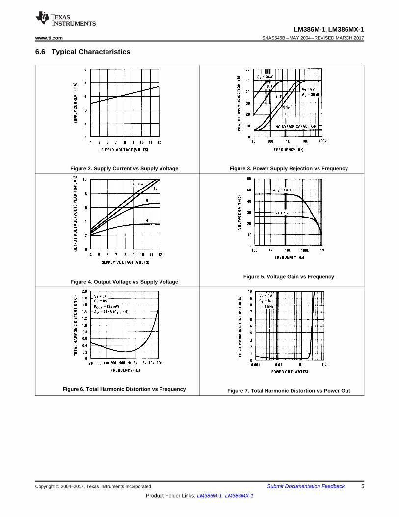
6.6 Typical Characteristics
Figure 2. Supply Current vs Supply Voltage Figure 3. Power Supply Rejection vs Frequency
Figure 4. Output Voltage vs Supply VoltageFigure 5. Voltage Gain vs Frequency
Figure 6. Total Harmonic Distortion vs Frequency Figure 7. Total Harmonic Distortion vs Power Out

6
LM386M-1, LM386MX-1SNAS545B –MAY 2004–REVISED MARCH 2017 www.ti.com
Product Folder Links: LM386M-1 LM386MX-1
Submit Documentation Feedback Copyright © 2004–2017, Texas Instruments Incorporated
Typical Characteristics (continued)
Figure 8. Device Dissipation vs Output Power Figure 9. Device Dissipation vs Output Power
Figure 10. Device Dissipation vs Output Power
7 Parameter Measurement Information
All parameters are measured according to the conditions described in the Specifications section.

+
-
GainCircuitry
BiasCircuitry
Bypass
7
LM386M-1, LM386MX-1www.ti.com SNAS545B –MAY 2004–REVISED MARCH 2017
Product Folder Links: LM386M-1 LM386MX-1
Submit Documentation FeedbackCopyright © 2004–2017, Texas Instruments Incorporated
8 Detailed Description
8.1 OverviewThe LM386 is a mono low voltage amplifier that can be used in a variety of applications. It can drive loads from 4Ω to 32 Ω. The gain is internally set to 20 but it can be modified from 20 to 200 by placing a resistor andcapacitor between pins 1 and 8. This device comes in three different 8-pin packages as PDIP, SOIC and VSSOPto fit in different applications.
8.2 Functional Block Diagram
8.3 Feature DescriptionThere is an internal 1.35-KΩ resistor that sets the gain of this device to 20. The gain can be modified from 20 to200. Detailed information about gain setting can be found in the Detailed Design Procedure section.
8.4 Device Functional ModesAs this is an Op Amp it can be used in different configurations to fit in several applications. The internal gainsetting resistor allows the LM386 to be used in a very low part count system. In addition a series resistor can beplaced between pins 1 and 5 to modify the gain and frequency response for specific applications.

VIN
10 k3
4
26
1
7
8
5
10
0.05 µF
250 µF +
+
-
LM386
Copyright © 2017, Texas Instruments Incorporated
8
LM386M-1, LM386MX-1SNAS545B –MAY 2004–REVISED MARCH 2017 www.ti.com
Product Folder Links: LM386M-1 LM386MX-1
Submit Documentation Feedback Copyright © 2004–2017, Texas Instruments Incorporated
9 Application and Implementation
NOTEInformation in the following applications sections is not part of the TI componentspecification, and TI does not warrant its accuracy or completeness. TI’s customers areresponsible for determining suitability of components for their purposes. Customers shouldvalidate and test their design implementation to confirm system functionality.
9.1 Application InformationBelow are shown different setups that show how the LM386 can be implemented in a variety of applications.
9.2 Typical Application
9.2.1 LM386 with Gain = 20Figure 11 shows the minimum part count application that can be implemented using LM386. Its gain is internallyset to 20.
Figure 11. LM386 with Gain = 20
9.2.1.1 Design Requirements
DESIGN PARAMETER EXAMPLE VALUELoad Impedance 4 Ω to 32 Ω
Supply Voltage 5 Ω to 12 Ω
9.2.1.2 Detailed Design Procedure
9.2.1.2.1 Gain Control
To make the LM386 a more versatile amplifier, two pins (1 and 8) are provided for gain control. With pins 1 and 8open the 1.35-kW resistor sets the gain at 20 (26 dB). If a capacitor is put from pin 1 to 8, bypassing the 1.35-kWresistor, the gain will go up to 200 (46 dB). If a resistor is placed in series with the capacitor, the gain can be setto any value from 20 to 200. Gain control can also be done by capacitively coupling a resistor (or FET) from pin 1to ground.
Additional external components can be placed in parallel with the internal feedback resistors to tailor the gain andfrequency response for individual applications. For example, we can compensate poor speaker bass response byfrequency shaping the feedback path. This is done with a series RC from pin 1 to 5 (paralleling the internal 15-kW resistor). For 6 dB effective bass boost: R . 15 kW, the lowest value for good stable operation is R = 10 kW ifpin 8 is open. If pins 1 and 8 are bypassed then R as low as 2 kW can be used. This restriction is because theamplifier is only compensated for closed-loop gains greater than 9.

VIN
10 k3
4
26
1
7
8
5
10
0.05 µF
250 µF +
+
-
LM386
+10 µF VS
BYPASS
Copyright © 2017, Texas Instruments Incorporated
9
LM386M-1, LM386MX-1www.ti.com SNAS545B –MAY 2004–REVISED MARCH 2017
Product Folder Links: LM386M-1 LM386MX-1
Submit Documentation FeedbackCopyright © 2004–2017, Texas Instruments Incorporated
9.2.1.2.2 Input Biasing
The schematic shows that both inputs are biased to ground with a 50 kW resistor. The base current of the inputtransistors is about 250 nA, so the inputs are at about 12.5 mV when left open. If the dc source resistance drivingthe LM386 is higher than 250 kW it will contribute very little additional offset (about 2.5 mV at the input, 50 mV atthe output). If the dc source resistance is less than 10 kW, then shorting the unused input to ground will keep theoffset low (about 2.5 mV at the input, 50 mV at the output). For dc source resistances between these values wecan eliminate excess offset by putting a resistor from the unused input to ground, equal in value to the dc sourceresistance. Of course all offset problems are eliminated if the input is capacitively coupled.
When using the LM386 with higher gains (bypassing the 1.35 kW resistor between pins 1 and 8) it is necessaryto bypass the unused input, preventing degradation of gain and possible instabilities. This is done with a 0.1 μFcapacitor or a short to ground depending on the dc source resistance on the driven input.
9.2.1.3 Application Curves
Figure 12. Voltage Gain vs Frequency
9.2.2 LM386 with Gain = 200
Figure 13. LM386 with Gain = 200
9.2.2.1 Design Requirements
DESIGN PARAMETER EXAMPLE VALUELoad Impedance 4 Ω to 32 Ω
Supply Voltage 5 Ω to 12 Ω

VIN
10 k3
4
26
1
7
8
5
10
0.05 µF
250 µF +
+
-
LM386
VS
BYPASS
1.2 k
Copyright © 2017, Texas Instruments Incorporated
10 µF
10
LM386M-1, LM386MX-1SNAS545B –MAY 2004–REVISED MARCH 2017 www.ti.com
Product Folder Links: LM386M-1 LM386MX-1
Submit Documentation Feedback Copyright © 2004–2017, Texas Instruments Incorporated
9.2.2.2 Detailed Design ProcedureThe Detailed Design Procedure can be found in the Detailed Design Procedure section.
9.2.2.3 Application Curves
Figure 14. Voltage Gain vs Frequency
9.2.3 LM386 with Gain = 50
Figure 15. LM386 with Gain = 200
9.2.3.1 Design Requirements
DESIGN PARAMETER EXAMPLE VALUELoad Impedance 4 Ω to 32 Ω
Supply Voltage 5 Ω to 12 Ω

3 V ± 15mA3
26
1
7
8
5
10
50 µF
+
+
-
LM386
+10 µF VS
47 k
4
0.01 µF BYPASS
390
VO
0.05 µF
4.7 k
0.01 µF
RL
ELDEMACF-S-2158
f = 1 kHz
Copyright © 2017, Texas Instruments Incorporated
11
LM386M-1, LM386MX-1www.ti.com SNAS545B –MAY 2004–REVISED MARCH 2017
Product Folder Links: LM386M-1 LM386MX-1
Submit Documentation FeedbackCopyright © 2004–2017, Texas Instruments Incorporated
9.2.3.2 Detailed Design ProcedureThe Detailed Design Procedure can be found in the Detailed Design Procedure section.
9.2.3.3 Application Curves
Figure 16. Voltage Gain vs Frequency
9.2.4 Low Distortion Power Wienbridge Oscillator
Figure 17. Low Distortion Power Wienbridge Oscillator
9.2.4.1 Design Requirements
DESIGN PARAMETER EXAMPLE VALUELoad Impedance 4 Ω to 32 Ω
Supply Voltage 5 Ω to 12 Ω

VIN
10 k3
4
26
7
8
5
0.05 µF
250 µF +
+
-
LM386
VS
10 ��
RL0.033 µF
10 k
1
VO
BYPASS
Copyright © 2017, Texas Instruments Incorporated
12
LM386M-1, LM386MX-1SNAS545B –MAY 2004–REVISED MARCH 2017 www.ti.com
Product Folder Links: LM386M-1 LM386MX-1
Submit Documentation Feedback Copyright © 2004–2017, Texas Instruments Incorporated
9.2.4.2 Detailed Design ProcedureThe Detailed Design Procedure can be found in the Detailed Design Procedure section.
9.2.4.3 Application Curves
Figure 18. Voltage Gain vs Frequency
9.2.5 LM386 with Bass Boost
Figure 19. LM386 with Bass Boost
9.2.5.1 Design Requirements
DESIGN PARAMETER EXAMPLE VALUELoad Impedance 4 Ω to 32 Ω
Supply Voltage 5 Ω to 12 Ω

3 4
26
1
8
5
10 k
+
-
LM386
VS
1 k
50 µF+
30 k
f = 1 kHz
0.1 µF
RL
VO
Copyright © 2017, Texas Instruments Incorporated
13
LM386M-1, LM386MX-1www.ti.com SNAS545B –MAY 2004–REVISED MARCH 2017
Product Folder Links: LM386M-1 LM386MX-1
Submit Documentation FeedbackCopyright © 2004–2017, Texas Instruments Incorporated
9.2.5.2 Detailed Design ProcedureThe Detailed Design Procedure can be found in the Detailed Design Procedure section.
9.2.5.3 Application Curves
Figure 20. Voltage Gain vs Frequency
9.2.6 Square Wave Oscillator
Figure 21. Square Wave Oscillator
9.2.6.1 Design Requirements
DESIGN PARAMETER EXAMPLE VALUELoad Impedance 4 Ω to 32 Ω
Supply Voltage 5 Ω to 12 Ω
3
4
26
8 5
+
-
LM386
BYPASSR1
10 k
VS
CC
VOL
10 k C12200 pF
0.05 µF
10 µF+
7
1
+
10 µFFROMDETECTOR
8 �SPEAKER
0.05 µF
+
+
47
250 µFFERRITE
BEAD
Copyright © 2017, Texas Instruments Incorporated
14
LM386M-1, LM386MX-1SNAS545B –MAY 2004–REVISED MARCH 2017 www.ti.com
Product Folder Links: LM386M-1 LM386MX-1
Submit Documentation Feedback Copyright © 2004–2017, Texas Instruments Incorporated
9.2.6.2 Detailed Design ProcedureThe Detailed Design Procedure can be found in the Detailed Design Procedure section.
9.2.6.3 Application Curves
Figure 22. Voltage Gain vs Frequency
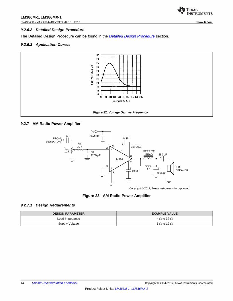
9.2.7 AM Radio Power Amplifier
Figure 23. AM Radio Power Amplifier
9.2.7.1 Design Requirements
DESIGN PARAMETER EXAMPLE VALUELoad Impedance 4 Ω to 32 Ω
Supply Voltage 5 Ω to 12 Ω

15
LM386M-1, LM386MX-1www.ti.com SNAS545B –MAY 2004–REVISED MARCH 2017
Product Folder Links: LM386M-1 LM386MX-1
Submit Documentation FeedbackCopyright © 2004–2017, Texas Instruments Incorporated
9.2.7.2 Detailed Design ProcedureThe Detailed Design Procedure can be found in the Detailed Design Procedure section.
9.2.7.3 Application Curves
Figure 24. Voltage Gain vs Frequency
10 Power Supply RecommendationsThe LM386 is specified for operation up to 12 V or 18 V. The power supply should be well regulated and thevoltage must be within the specified values. It is recommended to place a capacitor to GND close to the LM386power supply pin.

OUTPUT
LM386 10
0.05uF
250uF
INPUT
Connection to ground plane Connection to power 5V
Top layer traces Top layer ground plane
OUTPUT
LM38610
0.05uF
250uF
INPUT
Connection to ground plane Connection to power 5V
Top layer traces Top layer ground plane
16
LM386M-1, LM386MX-1SNAS545B –MAY 2004–REVISED MARCH 2017 www.ti.com
Product Folder Links: LM386M-1 LM386MX-1
Submit Documentation Feedback Copyright © 2004–2017, Texas Instruments Incorporated
11 Layout
11.1 Layout GuidelinesPlace all required components as close as possible to the device. Use short traces for the output to the speakerconnection. Route the analog traces far from the digital signal traces and avoid crossing them.
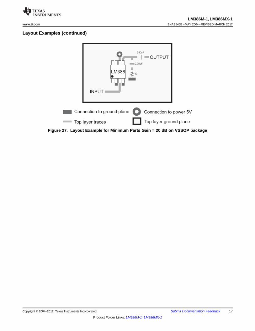
11.2 Layout Examples
Figure 25. Layout Example for Minimum Parts Gain = 20 dB on PDIP package
Figure 26. Layout Example for Minimum Parts Gain = 20 dB on SOIC package
LM386
INPUT
OUTPUT
10
0.05uF
250uF
Connection to ground plane Connection to power 5V
Top layer traces Top layer ground plane
17
LM386M-1, LM386MX-1www.ti.com SNAS545B –MAY 2004–REVISED MARCH 2017
Product Folder Links: LM386M-1 LM386MX-1
Submit Documentation FeedbackCopyright © 2004–2017, Texas Instruments Incorporated
Layout Examples (continued)
Figure 27. Layout Example for Minimum Parts Gain = 20 dB on VSSOP package

18
LM386M-1, LM386MX-1SNAS545B –MAY 2004–REVISED MARCH 2017 www.ti.com
Product Folder Links: LM386M-1 LM386MX-1
Submit Documentation Feedback Copyright © 2004–2017, Texas Instruments Incorporated
12 Device and Documentation Support
12.1 Device Support
12.1.1 Development Support
12.2 Documentation Support
12.3 Related Documentation
12.4 Related LinksThe table below lists quick access links. Categories include technical documents, support and communityresources, tools and software, and quick access to sample or buy.
Table 1. Related Links
PARTS PRODUCT FOLDER SAMPLE & BUY TECHNICALDOCUMENTS
TOOLS &SOFTWARE
SUPPORT &COMMUNITY
LM386M-1 Click here Click here Click here Click here Click hereLM386MX-1 Click here Click here Click here Click here Click here
12.5 Community ResourcesThe following links connect to TI community resources. Linked contents are provided "AS IS" by the respectivecontributors. They do not constitute TI specifications and do not necessarily reflect TI's views; see TI's Terms ofUse.
TI E2E™ Online Community TI's Engineer-to-Engineer (E2E) Community. Created to foster collaborationamong engineers. At e2e.ti.com, you can ask questions, share knowledge, explore ideas and helpsolve problems with fellow engineers.
Design Support TI's Design Support Quickly find helpful E2E forums along with design support tools andcontact information for technical support.
12.6 TrademarksE2E is a trademark of Texas Instruments.All other trademarks are the property of their respective owners.
12.7 Electrostatic Discharge CautionThese devices have limited built-in ESD protection. The leads should be shorted together or the device placed in conductive foamduring storage or handling to prevent electrostatic damage to the MOS gates.
12.8 GlossarySLYZ022 — TI Glossary.
This glossary lists and explains terms, acronyms, and definitions.

19
LM386M-1, LM386MX-1www.ti.com SNAS545B –MAY 2004–REVISED MARCH 2017
Product Folder Links: LM386M-1 LM386MX-1
Submit Documentation FeedbackCopyright © 2004–2017, Texas Instruments Incorporated
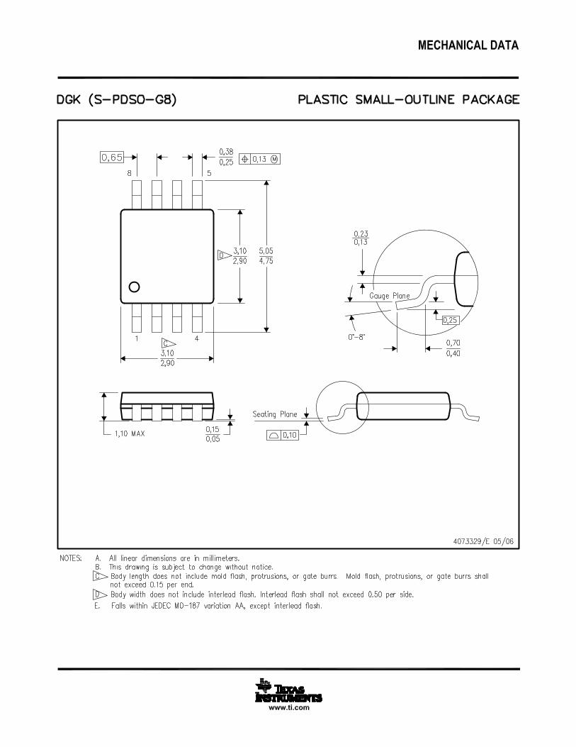
13 Mechanical, Packaging, and Orderable InformationThe following pages include mechanical, packaging, and orderable information. This information is the mostcurrent data available for the designated devices. This data is subject to change without notice and revision ofthis document. For browser-based versions of this data sheet, refer to the left-hand navigation.

PACKAGE OPTION ADDENDUM
www.ti.com 17-Jan-2017
Addendum-Page 1
PACKAGING INFORMATION
Orderable Device Status(1)
Package Type PackageDrawing
Pins PackageQty
Eco Plan(2)
Lead/Ball Finish(6)
MSL Peak Temp(3)
Op Temp (°C) Device Marking(4/5)
Samples
LM386M-1 ACTIVE SOIC D 8 95 TBD Call TI Call TI 0 to 70 LM386M-1
LM386M-1/NOPB ACTIVE SOIC D 8 95 Green (RoHS& no Sb/Br)
CU SN Level-1-260C-UNLIM 0 to 70 LM386M-1
LM386MMX-1/NOPB ACTIVE VSSOP DGK 8 3500 Green (RoHS& no Sb/Br)
CU SN Level-1-260C-UNLIM 0 to 70 Z86
LM386MX-1/NOPB ACTIVE SOIC D 8 2500 Green (RoHS& no Sb/Br)
CU SN Level-1-260C-UNLIM 0 to 70 LM386M-1
LM386N-1/NOPB ACTIVE PDIP P 8 40 Green (RoHS& no Sb/Br)
CU SN | Call TI Level-1-NA-UNLIM 0 to 70 LM386N-1
LM386N-3/NOPB ACTIVE PDIP P 8 40 Green (RoHS& no Sb/Br)
CU SN Level-1-NA-UNLIM 0 to 70 LM386N-3
LM386N-4/NOPB ACTIVE PDIP P 8 40 Green (RoHS& no Sb/Br)
CU SN | Call TI Level-1-NA-UNLIM 0 to 70 LM386N-4
(1) The marketing status values are defined as follows:ACTIVE: Product device recommended for new designs.LIFEBUY: TI has announced that the device will be discontinued, and a lifetime-buy period is in effect.NRND: Not recommended for new designs. Device is in production to support existing customers, but TI does not recommend using this part in a new design.PREVIEW: Device has been announced but is not in production. Samples may or may not be available.OBSOLETE: TI has discontinued the production of the device.
(2) Eco Plan - The planned eco-friendly classification: Pb-Free (RoHS), Pb-Free (RoHS Exempt), or Green (RoHS & no Sb/Br) - please check http://www.ti.com/productcontent for the latest availabilityinformation and additional product content details.TBD: The Pb-Free/Green conversion plan has not been defined.Pb-Free (RoHS): TI's terms "Lead-Free" or "Pb-Free" mean semiconductor products that are compatible with the current RoHS requirements for all 6 substances, including the requirement thatlead not exceed 0.1% by weight in homogeneous materials. Where designed to be soldered at high temperatures, TI Pb-Free products are suitable for use in specified lead-free processes.Pb-Free (RoHS Exempt): This component has a RoHS exemption for either 1) lead-based flip-chip solder bumps used between the die and package, or 2) lead-based die adhesive used betweenthe die and leadframe. The component is otherwise considered Pb-Free (RoHS compatible) as defined above.Green (RoHS & no Sb/Br): TI defines "Green" to mean Pb-Free (RoHS compatible), and free of Bromine (Br) and Antimony (Sb) based flame retardants (Br or Sb do not exceed 0.1% by weightin homogeneous material)
(3) MSL, Peak Temp. - The Moisture Sensitivity Level rating according to the JEDEC industry standard classifications, and peak solder temperature.
(4) There may be additional marking, which relates to the logo, the lot trace code information, or the environmental category on the device.

PACKAGE OPTION ADDENDUM
www.ti.com 17-Jan-2017
Addendum-Page 2
(5) Multiple Device Markings will be inside parentheses. Only one Device Marking contained in parentheses and separated by a "~" will appear on a device. If a line is indented then it is a continuationof the previous line and the two combined represent the entire Device Marking for that device.
(6) Lead/Ball Finish - Orderable Devices may have multiple material finish options. Finish options are separated by a vertical ruled line. Lead/Ball Finish values may wrap to two lines if the finishvalue exceeds the maximum column width.
Important Information and Disclaimer:The information provided on this page represents TI's knowledge and belief as of the date that it is provided. TI bases its knowledge and belief on informationprovided by third parties, and makes no representation or warranty as to the accuracy of such information. Efforts are underway to better integrate information from third parties. TI has taken andcontinues to take reasonable steps to provide representative and accurate information but may not have conducted destructive testing or chemical analysis on incoming materials and chemicals.TI and TI suppliers consider certain information to be proprietary, and thus CAS numbers and other limited information may not be available for release.
In no event shall TI's liability arising out of such information exceed the total purchase price of the TI part(s) at issue in this document sold by TI to Customer on an annual basis.

TAPE AND REEL INFORMATION
*All dimensions are nominal
Device PackageType
PackageDrawing
Pins SPQ ReelDiameter
(mm)
ReelWidth
W1 (mm)
A0(mm)
B0(mm)
K0(mm)
P1(mm)
W(mm)
Pin1Quadrant
LM386MMX-1/NOPB VSSOP DGK 8 3500 330.0 12.4 5.3 3.4 1.4 8.0 12.0 Q1
LM386MX-1/NOPB SOIC D 8 2500 330.0 12.4 6.5 5.4 2.0 8.0 12.0 Q1
PACKAGE MATERIALS INFORMATION
www.ti.com 17-Jan-2017
Pack Materials-Page 1

*All dimensions are nominal
Device Package Type Package Drawing Pins SPQ Length (mm) Width (mm) Height (mm)
LM386MMX-1/NOPB VSSOP DGK 8 3500 367.0 367.0 35.0
LM386MX-1/NOPB SOIC D 8 2500 367.0 367.0 35.0
PACKAGE MATERIALS INFORMATION
www.ti.com 17-Jan-2017
Pack Materials-Page 2


IMPORTANT NOTICE FOR TI DESIGN INFORMATION AND RESOURCES
Texas Instruments Incorporated (‘TI”) technical, application or other design advice, services or information, including, but not limited to,reference designs and materials relating to evaluation modules, (collectively, “TI Resources”) are intended to assist designers who aredeveloping applications that incorporate TI products; by downloading, accessing or using any particular TI Resource in any way, you(individually or, if you are acting on behalf of a company, your company) agree to use it solely for this purpose and subject to the terms ofthis Notice.TI’s provision of TI Resources does not expand or otherwise alter TI’s applicable published warranties or warranty disclaimers for TIproducts, and no additional obligations or liabilities arise from TI providing such TI Resources. TI reserves the right to make corrections,enhancements, improvements and other changes to its TI Resources.You understand and agree that you remain responsible for using your independent analysis, evaluation and judgment in designing yourapplications and that you have full and exclusive responsibility to assure the safety of your applications and compliance of your applications(and of all TI products used in or for your applications) with all applicable regulations, laws and other applicable requirements. Yourepresent that, with respect to your applications, you have all the necessary expertise to create and implement safeguards that (1)anticipate dangerous consequences of failures, (2) monitor failures and their consequences, and (3) lessen the likelihood of failures thatmight cause harm and take appropriate actions. You agree that prior to using or distributing any applications that include TI products, youwill thoroughly test such applications and the functionality of such TI products as used in such applications. TI has not conducted anytesting other than that specifically described in the published documentation for a particular TI Resource.You are authorized to use, copy and modify any individual TI Resource only in connection with the development of applications that includethe TI product(s) identified in such TI Resource. NO OTHER LICENSE, EXPRESS OR IMPLIED, BY ESTOPPEL OR OTHERWISE TOANY OTHER TI INTELLECTUAL PROPERTY RIGHT, AND NO LICENSE TO ANY TECHNOLOGY OR INTELLECTUAL PROPERTYRIGHT OF TI OR ANY THIRD PARTY IS GRANTED HEREIN, including but not limited to any patent right, copyright, mask work right, orother intellectual property right relating to any combination, machine, or process in which TI products or services are used. Informationregarding or referencing third-party products or services does not constitute a license to use such products or services, or a warranty orendorsement thereof. Use of TI Resources may require a license from a third party under the patents or other intellectual property of thethird party, or a license from TI under the patents or other intellectual property of TI.TI RESOURCES ARE PROVIDED “AS IS” AND WITH ALL FAULTS. TI DISCLAIMS ALL OTHER WARRANTIES ORREPRESENTATIONS, EXPRESS OR IMPLIED, REGARDING TI RESOURCES OR USE THEREOF, INCLUDING BUT NOT LIMITED TOACCURACY OR COMPLETENESS, TITLE, ANY EPIDEMIC FAILURE WARRANTY AND ANY IMPLIED WARRANTIES OFMERCHANTABILITY, FITNESS FOR A PARTICULAR PURPOSE, AND NON-INFRINGEMENT OF ANY THIRD PARTY INTELLECTUALPROPERTY RIGHTS.TI SHALL NOT BE LIABLE FOR AND SHALL NOT DEFEND OR INDEMNIFY YOU AGAINST ANY CLAIM, INCLUDING BUT NOTLIMITED TO ANY INFRINGEMENT CLAIM THAT RELATES TO OR IS BASED ON ANY COMBINATION OF PRODUCTS EVEN IFDESCRIBED IN TI RESOURCES OR OTHERWISE. IN NO EVENT SHALL TI BE LIABLE FOR ANY ACTUAL, DIRECT, SPECIAL,COLLATERAL, INDIRECT, PUNITIVE, INCIDENTAL, CONSEQUENTIAL OR EXEMPLARY DAMAGES IN CONNECTION WITH ORARISING OUT OF TI RESOURCES OR USE THEREOF, AND REGARDLESS OF WHETHER TI HAS BEEN ADVISED OF THEPOSSIBILITY OF SUCH DAMAGES.You agree to fully indemnify TI and its representatives against any damages, costs, losses, and/or liabilities arising out of your non-compliance with the terms and provisions of this Notice.This Notice applies to TI Resources. Additional terms apply to the use and purchase of certain types of materials, TI products and services.These include; without limitation, TI’s standard terms for semiconductor products http://www.ti.com/sc/docs/stdterms.htm), evaluationmodules, and samples (http://www.ti.com/sc/docs/sampterms.htm).
Mailing Address: Texas Instruments, Post Office Box 655303, Dallas, Texas 75265Copyright © 2017, Texas Instruments Incorporated