lm4041-n/lm4041-n-q1 precision micropower shunt voltage
TRANSCRIPT

LM4041-N, LM4041-N-Q1
www.ti.com SNOS641F –OCTOBER 1999–REVISED JULY 2013
LM4041-N/LM4041-N-Q1 Precision Micropower Shunt Voltage ReferenceCheck for Samples: LM4041-N, LM4041-N-Q1
1FEATURES DESCRIPTIONIdeal for space critical applications, the LM4041-N
2• Available in Standard, AEC Q-100 Grade 1precision voltage reference is available in the sub-(Extended Temp. Range) and Grade 3miniature SC70 and SOT-23 surface-mount(Industrial Temp. Range) Qualified Versionspackages. The LM4041-N's advanced design
(SOT-23 only) eliminates the need for an external stabilizing• Small Packages: SOT-23, TO-92, and SC70 capacitor while ensuring stability with any capacitive
load, thus making the LM4041-N easy to use. Further• No Output Capacitor Requiredreducing design effort is the availability of a fixed• Tolerates Capacitive Loads(1.225V) and adjustable reverse breakdown voltage.
• Reverse Breakdown Voltage Options of 1.225V The minimum operating current is 60 μA for theand Adjustable LM4041-N 1.2 and the LM4041-N ADJ. Both versions
have a maximum operating current of 12 mA.APPLICATIONS
The LM4041-N utilizes fuse and zener-zap reverse• Portable, Battery-Powered Equipment breakdown or reference voltage trim during wafer sort
to ensure that the prime parts have an accuracy of• Data Acquisition Systemsbetter than ±0.1% (A grade) at 25°C. Bandgap
• Instrumentation reference temperature drift curvature correction and• Process Control low dynamic impedance ensure stable reverse
breakdown voltage accuracy over a wide range of• Energy Managementoperating temperatures and currents.
• Automotive
• Precision Audio Components
Key Specifications (LM4041-N/LM4041-N-Q1 1.2)
Output voltage tolerance (A grade, 25°C) ±0.1%(max)
Low output noise (10 Hz to 10kHz) 20μVrms
Wide operating current range 60μA to 12mA
Industrial temperature range (LM4041A/B-N, LM4041-N-Q1A/Q1B) −40°C to +85°C
Extended temperature range (LM4041C/D/E-N, LM4041-N-Q1C/Q1D/Q1E) −40°C to +125°C
Low temperature coefficient 100 ppm/°C (max)
Connection Diagrams
*This pin must be left floating or connected to pin 2.
Figure 1. SOT-23 - Top ViewSee Package Number DBZ0003A(JEDEC Registration TO-236AB)
1
Please be aware that an important notice concerning availability, standard warranty, and use in critical applications ofTexas Instruments semiconductor products and disclaimers thereto appears at the end of this data sheet.
2All trademarks are the property of their respective owners.
PRODUCTION DATA information is current as of publication date. Copyright © 1999–2013, Texas Instruments IncorporatedProducts conform to specifications per the terms of the TexasInstruments standard warranty. Production processing does notnecessarily include testing of all parameters.

1
2
3
-
+
5
FB
4N/C
ADJ
N/C
1
2
3
N/C*
-
+
5N/C
4N/C
LM4041-N, LM4041-N-Q1
SNOS641F –OCTOBER 1999–REVISED JULY 2013 www.ti.com
*This pin must be left floating or connected to pin 1.
Figure 2. SC70 - Top ViewSee Package Number DCK0005A
Figure 3. TO-92Bottom View
See Package Number LP0003A
These devices have limited built-in ESD protection. The leads should be shorted together or the device placed in conductive foamduring storage or handling to prevent electrostatic damage to the MOS gates.
Absolute Maximum Ratings (1) (2)
Reverse Current 20 mA
Forward Current 10 mA
Maximum Output Voltage (LM4041-N ADJ, LM4041-N-Q1 ADJ) 15V
Power Dissipation (TA = 25°C) (3) DBZ Package 306 mW
LP Package 550 mW
DCK Package 241mW
Storage Temperature −65°C to +150°C
Lead Temperature DBZ Packages Vapor phase (60 seconds) +215°C
Infrared (15 seconds) +220°C
LP Package Soldering (10 seconds) +260°C
ESD Susceptibility Human Body Model (4) 2 kV
Machine Model (4) 200V
See AN-450 “Surface Mounting Methods and Their Effect on Product Reliability” for other methods of soldering surface mount devicesSNOA472.
(1) Absolute Maximum Ratings indicate limits beyond which damage to the device may occur. Operating Ratings indicate conditions forwhich the device is functional, but do not ensure specific performance limits. For ensured specifications and test conditions, see theElectrical Characteristics. The ensured specifications apply only for the test conditions listed. Some performance characteristics maydegrade when the device is not operated under the listed test conditions.
(2) If Military/Aerospace specified devices are required, please contact the TI Sales Office/ Distributors for availability and specifications.(3) The maximum power dissipation must be derated at elevated temperatures and is dictated by TJmax (maximum junction temperature),
θJA (junction to ambient thermal resistance), and TA (ambient temperature). The maximum allowable power dissipation at anytemperature is PDmax = (TJmax − TA)/θJA or the number given in the Absolute Maximum Ratings, whichever is lower. For the LM4041-N,TJmax = 125°C, and the typical thermal resistance (θJA), when board mounted, is 326°C/W for the SOT-23 package, 415°C/W for theSC70 package and 180°C/W with 0.4″ lead length and 170°C/W with 0.125″ lead length for the TO-92 package.
(4) The human body model is a 100 pF capacitor discharged through a 1.5 kΩ resistor into each pin. The machine model is a 200 pFcapacitor discharged directly into each pin. All pins are rated at 2kV for Human Body Model, but the feedback pin which is rated at 1kV.
2 Submit Documentation Feedback Copyright © 1999–2013, Texas Instruments Incorporated
Product Folder Links: LM4041-N, LM4041-N-Q1

LM4041-N, LM4041-N-Q1
www.ti.com SNOS641F –OCTOBER 1999–REVISED JULY 2013
Operating Ratings (1) (2)
Temperature Range (Tmin ≤ TA ≤ Tmax)
Industrial Temperature Range −40°C ≤ TA ≤ +85°C
Extended Temperature Range −40°C ≤ TA ≤ +125°C
Reverse Current LM4041-N 1.2, LM4041-N-Q1 1.2 60 μA to 12 mA
LM4041-N ADJ, LM4041-N-Q1 ADJ 60 μA to 12 mA
Output Voltage Range LM4041-N ADJ, LM4041-N-Q1 ADJ 1.24V to 10V
(1) Absolute Maximum Ratings indicate limits beyond which damage to the device may occur. Operating Ratings indicate conditions forwhich the device is functional, but do not ensure specific performance limits. For ensured specifications and test conditions, see theElectrical Characteristics. The ensured specifications apply only for the test conditions listed. Some performance characteristics maydegrade when the device is not operated under the listed test conditions.
(2) The maximum power dissipation must be derated at elevated temperatures and is dictated by TJmax (maximum junction temperature),θJA (junction to ambient thermal resistance), and TA (ambient temperature). The maximum allowable power dissipation at anytemperature is PDmax = (TJmax − TA)/θJA or the number given in the Absolute Maximum Ratings, whichever is lower. For the LM4041-N,TJmax = 125°C, and the typical thermal resistance (θJA), when board mounted, is 326°C/W for the SOT-23 package, 415°C/W for theSC70 package and 180°C/W with 0.4″ lead length and 170°C/W with 0.125″ lead length for the TO-92 package.
LM4041-N/LM4041-N-Q1 1.2 Electrical Characteristics (Industrial Temperature Range)Boldface limits apply for TA = TJ = TMIN to TMAX; all other limits TA = TJ = 25°C. The grades A and B designate initialReverse Breakdown Voltage tolerances of ±0.1% and ±0.2%, respectively.
Symbol Parameter Conditions Typical (1) LM4041AIM3 LM4041BIM3 UnitsLM4041QAIM3 LM4041QBIM3 (Limit)LM4041AIM3 LM4041BIZLM4041AIZ LM4041BIM7
Limits (2) Limits (2)
VR Reverse Breakdown Voltage IR = 100 μA 1.225 V
Reverse Breakdown Voltage IR = 100 μA ±1.2 ±2.4 mV (max)Tolerance (3)
±9.2 ±10.4 mV (max)
IRMIN Minimum Operating Current 45 μA
60 60 μA (max)
65 65 μA (max)
ΔVR/ΔT Average Reverse Breakdown IR= 10 mA ±20 ppm/°CVoltage Temperature IR = 1 mA ±15 ±100 ±100 ppm/°C (max)Coefficient (3)
IR = 100 μA ±15 ppm/°C
(1) Typicals are at TJ = 25°C and represent most likely parametric norm.(2) Limits are 100% production tested at 25°C. Limits over temperature are ensured through correlation using Statistical Quality Control
(SQC) methods. The limits are used to calculate AOQL.(3) The boldface (over-temperature) limit for Reverse Breakdown Voltage Tolerance is defined as the room temperature Reverse
Breakdown Voltage Tolerance ±[(ΔVR↱ΔT)(max ΔT)(VR)]. Where, ΔVR/ΔT is the VR temperature coefficient, maxΔT is the maximumdifference in temperature from the reference point of 25 °C to T MAX or TMIN, and VR is the reverse breakdown voltage. The total over-temperature tolerance for the different grades in the industrial temperature range where maxΔT=65°C is shown below:A-grade: ±0.75% = ±0.1% ±100 ppm/°C × 65°CB-grade: ±0.85% = ±0.2% ±100 ppm/°C × 65°CC-grade: ±1.15% = ±0.5% ±100 ppm/°C × 65°CD-grade: ±1.98% = ±1.0% ±150 ppm/°C × 65°CE-grade: ±2.98% = ±2.0% ±150 ppm/°C × 65°CThe total over-temperature tolerance for the different grades in the extended temperature range where max ΔT = 100 °C is shownbelow:B-grade: ±1.2% = ±0.2% ±100 ppm/°C × 100°CC-grade: ±1.5% = ±0.5% ±100 ppm/°C × 100°CD-grade: ±2.5% = ±1.0% ±150 ppm/°C × 100°CE-grade: ±4.5% = ±2.0% ±150 ppm/°C × 100°CTherefore, as an example, the A-grade LM4041-N 1.2 has an over-temperature Reverse Breakdown Voltage tolerance of ±1.2V × 0.75%= ±9.2 mV.
Copyright © 1999–2013, Texas Instruments Incorporated Submit Documentation Feedback 3
Product Folder Links: LM4041-N, LM4041-N-Q1

LM4041-N, LM4041-N-Q1
SNOS641F –OCTOBER 1999–REVISED JULY 2013 www.ti.com
LM4041-N/LM4041-N-Q1 1.2 Electrical Characteristics (Industrial TemperatureRange) (continued)Boldface limits apply for TA = TJ = TMIN to TMAX; all other limits TA = TJ = 25°C. The grades A and B designate initialReverse Breakdown Voltage tolerances of ±0.1% and ±0.2%, respectively.
Symbol Parameter Conditions Typical (1) LM4041AIM3 LM4041BIM3 UnitsLM4041QAIM3 LM4041QBIM3 (Limit)LM4041AIM3 LM4041BIZLM4041AIZ LM4041BIM7
Limits (2) Limits (2)
ΔVR/ΔIR Reverse Breakdown Voltage IRMIN ≤ IR ≤ 1 mA 0.7 mVChange with Operating 1.5 1.5 mV (max)Current Change (4)
2.0 2.0 mV (max)
1 mA ≤ IR ≤ 12 mA 4.0 mV
6.0 6.0 mV (max)
8.0 8.0 mV (max)
ZR Reverse Dynamic Impedance IR = 1 mA, f = 120 Hz, 0.5 ΩIAC= 0.1 IR 1.5 1.5 Ω (max)
eN Wideband Noise IR = 100 μA 20 μVrms10 Hz ≤ f ≤ 10 kHz
ΔVR Reverse Breakdown Voltage t = 1000 hrsLong Term Stability T = 25°C ±0.1°C 120 ppm
IR = 100 μA
VHYST Thermal Hysteresis (5) ΔT = −40°C to0.08 %
+125°C
(4) Load regulation is measured on pulse basis from no load to the specified load current. Ouput changes due to die temperature changemust be taken into account separately.-
(5) Thermal hysteresis is defined as the difference in voltage measured at +25°C after cycling to temperature -40°C and the 25°Cmeasurement after cycling to temperature +125°C.
4 Submit Documentation Feedback Copyright © 1999–2013, Texas Instruments Incorporated
Product Folder Links: LM4041-N, LM4041-N-Q1

LM4041-N, LM4041-N-Q1
www.ti.com SNOS641F –OCTOBER 1999–REVISED JULY 2013
LM4041-N/LM4041-N-Q1 1.2 Electrical Characteristics (Industrial Temperature Range)Boldface limits apply for TA = TJ = TMINto TMAX; all other limits TA = TJ = 25°C. The grades C, D and E designate initialReverse Breakdown Voltage tolerances of ±0.5%, ±1.0% and ±2.0%, respectively.
Symbol Parameter Conditions Typical (1) LM4041CIM3 LM4041DIM3 LM4041EIM3 UnitsLM4041QCIM3 LM4041QDIM3 LM4041QEIM3 (Limit)
LM4041CIZ LM4041DIZ LM4041EIZLM4041CIM7 LM4041DIM7 LM4041EIM7
Limits (2) Limits (2) Limits (2)
VR Reverse Breakdown IR = 100 μA 1.225 VVoltage
Reverse Breakdown IR = 100 μA ±6 ±12 ±25 mV (max)Voltage Tolerance (3)
±14 ±24 ±36 mV (max)
IRMIN Minimum Operating 45 μACurrent 60 65 65 μA (max)
65 70 70 μA (max)
ΔVR/ΔT VR Temperature IR = 10 mA ±20 ppm/°CCoefficient (3)
IR = 1 mA ±15 ±100 ±150 ±150 ppm/°C (max)
IR= 100 μA ±15 ppm/°C
ΔVR/ΔIR Reverse Breakdown IRMIN ≤ IR ≤ 1 mA 0.7 mVVoltage Change with 1.5 2.0 2.0 mV (max)Operating Current
2.0 2.5 2.5 mV (max)Change (4)
1 mA ≤ IR ≤ 12 mA 2.5 mV
6.0 8.0 8.0 mV (max)
8.0 10.0 10.0 mV (max)
ZR Reverse Dynamic IR = 1 mA, f = 120 0.5 ΩImpedance Hz Ω(max)
IAC = 0.1 IR 1.5 2.0 2.0
eN Wideband Noise IR = 100 μA 20 μVrms10 Hz ≤ f ≤ 10 kHz
ΔVR Reverse Breakdown t = 1000 hrsVoltage Long Term T = 25°C ±0.1°C 120 ppmStability IR = 100 μA
VHYST Thermal Hysteresis (5) ΔT = −40°C to0.08 %
+125°C
(1) Typicals are at TJ = 25°C and represent most likely parametric norm.(2) Limits are 100% production tested at 25°C. Limits over temperature are ensured through correlation using Statistical Quality Control
(SQC) methods. The limits are used to calculate AOQL.(3) The boldface (over-temperature) limit for Reverse Breakdown Voltage Tolerance is defined as the room temperature Reverse
Breakdown Voltage Tolerance ±[(ΔVR↱ΔT)(max ΔT)(VR)]. Where, ΔVR/ΔT is the VR temperature coefficient, maxΔT is the maximumdifference in temperature from the reference point of 25 °C to T MAX or TMIN, and VR is the reverse breakdown voltage. The total over-temperature tolerance for the different grades in the industrial temperature range where maxΔT=65°C is shown below:A-grade: ±0.75% = ±0.1% ±100 ppm/°C × 65°CB-grade: ±0.85% = ±0.2% ±100 ppm/°C × 65°CC-grade: ±1.15% = ±0.5% ±100 ppm/°C × 65°CD-grade: ±1.98% = ±1.0% ±150 ppm/°C × 65°CE-grade: ±2.98% = ±2.0% ±150 ppm/°C × 65°CThe total over-temperature tolerance for the different grades in the extended temperature range where max ΔT = 100 °C is shownbelow:B-grade: ±1.2% = ±0.2% ±100 ppm/°C × 100°CC-grade: ±1.5% = ±0.5% ±100 ppm/°C × 100°CD-grade: ±2.5% = ±1.0% ±150 ppm/°C × 100°CE-grade: ±4.5% = ±2.0% ±150 ppm/°C × 100°CTherefore, as an example, the A-grade LM4041-N 1.2 has an over-temperature Reverse Breakdown Voltage tolerance of ±1.2V × 0.75%= ±9.2 mV.
(4) Load regulation is measured on pulse basis from no load to the specified load current. Ouput changes due to die temperature changemust be taken into account separately.-
(5) Thermal hysteresis is defined as the difference in voltage measured at +25°C after cycling to temperature -40°C and the 25°Cmeasurement after cycling to temperature +125°C.
Copyright © 1999–2013, Texas Instruments Incorporated Submit Documentation Feedback 5
Product Folder Links: LM4041-N, LM4041-N-Q1

LM4041-N, LM4041-N-Q1
SNOS641F –OCTOBER 1999–REVISED JULY 2013 www.ti.com
LM4041-N/LM4041-N-Q1 1.2 Electrical Characteristics (Extended Temperature Range)Boldface limits apply for TA = TJ = TMINto TMAX; all other limits TA = TJ = 25°C. The grades C, D and E designate initialReverse Breakdown Voltage tolerance of ±0.5%, ±1.0% and ±2.0% respectively.
Symbol Parameter Conditions Typical (1) LM4041CEM3 LM4041DEM3 LM4041EEM3 UnitsLM4041QCEM3 LM4041QDEM3 LM4041QEEM3 (Limit)
Limits (2) Limits (2) Limits (2)
VR Reverse Breakdown IR = 100 μA 1.225 VVoltage
Reverse Breakdown IR = 100 μA ±6 ±12 ±25 mV (max)Voltage Error (3)
±18.4 ±31 ±43 mV (max)
IRMIN Minimum Operating 45 μACurrent 60 65 65 μA (max)
68 73 73 μA (max)
ΔVR/ΔT VR Temperature IR= 10 mA ±20 ppm/°CCoefficient (3)
IR = 1 mA ±15 ppm/°C±100 ±150 ±150
(max)
IR = 100 μA ±15 ppm/°C
ΔVR/ΔIR Reverse Breakdown IRMIN ≤ IR ≤ 1.0 mA 0.7 mVChange with 1.5 2.0 2.0 mV (max)Current (4)
2.0 2.5 2.5 mV (max)
1 mA ≤ IR ≤ 12 mA 2.5 mV
6.0 8.0 8.0 mV (max)
8.0 10.0 10.0 mV (max)
ZR Reverse Dynamic IR = 1 mA, f = 120 0.5 ΩImpedance Hz, Ω (max)
IAC= 0.1 IR 1.5 2.0 2.0
eN Noise Voltage IR = 100 μA20 μVrms10 Hz ≤ f ≤ 10 kHz
ΔVR Long Term Stability t = 1000 hrs(Non-Cumulative) T = 25°C ±0.1°C 120 ppm
IR = 100 μA
VHYST Thermal Hysteresis (5) ΔT = −40°C to0.08 %
+125°C
(1) Typicals are at TJ = 25°C and represent most likely parametric norm.(2) Limits are 100% production tested at 25°C. Limits over temperature are ensured through correlation using Statistical Quality Control
(SQC) methods. The limits are used to calculate AOQL.(3) The boldface (over-temperature) limit for Reverse Breakdown Voltage Tolerance is defined as the room temperature Reverse
Breakdown Voltage Tolerance ±[(ΔVR↱ΔT)(max ΔT)(VR)]. Where, ΔVR/ΔT is the VR temperature coefficient, maxΔT is the maximumdifference in temperature from the reference point of 25 °C to T MAX or TMIN, and VR is the reverse breakdown voltage. The total over-temperature tolerance for the different grades in the industrial temperature range where maxΔT=65°C is shown below:A-grade: ±0.75% = ±0.1% ±100 ppm/°C × 65°CB-grade: ±0.85% = ±0.2% ±100 ppm/°C × 65°CC-grade: ±1.15% = ±0.5% ±100 ppm/°C × 65°CD-grade: ±1.98% = ±1.0% ±150 ppm/°C × 65°CE-grade: ±2.98% = ±2.0% ±150 ppm/°C × 65°CThe total over-temperature tolerance for the different grades in the extended temperature range where max ΔT = 100 °C is shownbelow:B-grade: ±1.2% = ±0.2% ±100 ppm/°C × 100°CC-grade: ±1.5% = ±0.5% ±100 ppm/°C × 100°CD-grade: ±2.5% = ±1.0% ±150 ppm/°C × 100°CE-grade: ±4.5% = ±2.0% ±150 ppm/°C × 100°CTherefore, as an example, the A-grade LM4041-N 1.2 has an over-temperature Reverse Breakdown Voltage tolerance of ±1.2V × 0.75%= ±9.2 mV.
(4) Load regulation is measured on pulse basis from no load to the specified load current. Ouput changes due to die temperature changemust be taken into account separately.-
(5) Thermal hysteresis is defined as the difference in voltage measured at +25°C after cycling to temperature -40°C and the 25°Cmeasurement after cycling to temperature +125°C.
6 Submit Documentation Feedback Copyright © 1999–2013, Texas Instruments Incorporated
Product Folder Links: LM4041-N, LM4041-N-Q1

LM4041-N, LM4041-N-Q1
www.ti.com SNOS641F –OCTOBER 1999–REVISED JULY 2013
LM4041-N/LM4041-N-Q1 ADJ (Adjustable) Electrical Characteristics (Industrial TemperatureRange)Boldface limits apply for TA = TJ = TMINto TMAX; all other limits TJ = 25°C unless otherwise specified (SOT-23, see (1)),IRMIN ≤ IR ≤ 12 mA, VREF ≤ VOUT ≤ 10V. The grades C and D designate initial Reference Voltage Tolerances of ±0.5% and±1%, respectively for VOUT = 5V.
Symbol Parameter Conditions Typical (2) LM4041CIM3 LM4041DIM3 UnitsLM4041QCIM3 LM4041QDIM3 (Limit)
LM4041CIZ LM4041DIZLM4041CIM7 LM4041DIM7
(3) (3)
VREF Reference Voltage IR = 100 μA, VOUT = 5V 1.233 V
Reference Voltage IR = 100 μA, VOUT = 5V ±6.2 ±12 mV (max)Tolerance (4)
±14 ±24 mV (max)
IRMIN Minimum Operating 45 μACurrent 60 65 μA (max)
65 70 μA (max)
ΔVREF/ΔIR Reference Voltage IRMIN ≤ IR ≤ 1 mA 0.7 mVChange with Operating SOT-23: VOUT ≥ 1.6V (6)
1.5 2.0 mV (max)Current Change (5)
2.0 2.5 mV (max)
1 mA ≤ IR ≤ 12 mA 2 mVSOT-23: VOUT ≥ 1.6V (6)
4 6 mV (max)
6 8 mV (max)
ΔVREF/ΔV Reference Voltage IR = 1 mA −1.55 mV/VO Change with Output −2.0 −2.5 mV/V (max)
Voltage Change−2.5 −3.0 mV/V (max)
IFB Feedback Current 60 nA
100 150 nA (max)
120 200 nA (max)
ΔVREF/ΔT Average Reference VOUT = IR = 10 mA 20 ppm/°CVoltage Temperature 5V, IR = 1 mA 15 ±100 ±150 ppm/°C (max)Coefficient (4)
IR = 100 μA 15 ppm/°C
ZOUT Dynamic Output IR = 1 mA, f = 120 Hz,Impedance IAC = 0.1 IR
VOUT = VREF 0.3 ΩVOUT = 10V 2 Ω
eN Wideband Noise IR = 100 VOUT = VREF 20 μVrmsμA
10 Hz ≤ f ≤ 10 kHz
ΔVREF Reference Voltage Long t = 1000 hrs, IR = 100 μA, 120 ppmTerm Stability T = 25°C ±0.1°C
VHYST Thermal Hysteresis (7) ΔT = −40°C to +125°C 0.08 %
(1) When VOUT ≤ 1.6V, the LM4041-N ADJ in the SOT-23 package must operate at reduced IR. This is caused by the series resistance ofthe die attach between the die (-) output and the package (-) output pin. See the Output Saturation (SOT-23 only) curve in the TypicalPerformance Characteristics section.
(2) Typicals are at TJ = 25°C and represent most likely parametric norm.(3) Limits are 100% production tested at 25°C. Limits over temperature are ensured through correlation using Statistical Quality Control
(SQC) methods. The limits are used to calculate AOQL.(4) Reference voltage and temperature coefficient will change with output voltage. See Typical Performance Characteristics curves.(5) Load regulation is measured on pulse basis from no load to the specified load current. Ouput changes due to die temperature change
must be taken into account separately.-(6) When VOUT ≤ 1.6V, the LM4041-N ADJ in the SOT-23 package must operate at reduced IR. This is caused by the series resistance of
the die attach between the die (-) output and the package (-) output pin. See the Output Saturation (SOT-23 only) curve in the TypicalPerformance Characteristics section.
(7) Thermal hysteresis is defined as the difference in voltage measured at +25°C after cycling to temperature -40°C and the 25°Cmeasurement after cycling to temperature +125°C.
Copyright © 1999–2013, Texas Instruments Incorporated Submit Documentation Feedback 7
Product Folder Links: LM4041-N, LM4041-N-Q1

LM4041-N, LM4041-N-Q1
SNOS641F –OCTOBER 1999–REVISED JULY 2013 www.ti.com
LM4041-N/LM4041-N-Q1 ADJ (Adjustable) Electrical Characteristics (Extended TemperatureRange)Boldface limits apply for TA = TJ = TMINto TMAX; all other limits TJ = 25°C unless otherwise specified (SOT-23, see (1)), IRMIN
≤ IR ≤ 12 mA, VREF ≤ VOUT ≤ 10V. The grades C and D designate initial Reference Voltage Tolerances of ±0.5% and ±1%,respectively for VOUT = 5V.
Symbol Parameter Conditions Typical (2) LM4041CEM3 LM4041DEM3 UnitsLM4041QCEM3 (3) LM4041QDEM3 (3) (Limit)
VREF Reference Voltage IR = 100 μA, VOUT = 5V 1.233 V
Reference Voltage IR = 100 μA, VOUT = 5V ±6.2 ±12 mV (max)Tolerance (4)
±18 ±30 mV (max)
IRMIN Minimum Operating 45 μACurrent 60 65 μA (max)
68 73 μA (max)
ΔVREF/ΔIR Reference Voltage IRMIN ≤ IR ≤ 1 mA 0.7 mVChange with Operating SOT-23: VOUT ≥ 1.6V (1)
1.5 2.0 mV (max)Current Change (5)
2.0 2.5 mV (max)
1 mA ≤ IR ≤ 12 mA 2 mVSOT-23: VOUT ≥ 1.6V (1)
8 10 mV (max)
6 8 mV (max)
ΔVREF/ΔV Reference Voltage IR = 1 mA −1.55 mV/VO Change with Output −2.0 −2.5 mV/V (max)
Voltage Change−3.0 −4.0 mV/V (max)
IFB Feedback Current 60 nA
100 150 nA (max)
120 200 nA (max)
ΔVREF/ΔT Average Reference VOUT = 5V, IR = 10 20 ppm/°CVoltage Temperature mACoefficient (4)
IR = 1 15 ppm/°C±100 ±150
mA (max)
IR = 100 15 ppm/°CμA
ZOUT Dynamic Output IR = 1 mA, f = 120 Hz,Impedance IAC = 0.1 IR
VOUT =VREF 0.3 ΩVOUT = 2 Ω10V
eN Wideband Noise IR = 100 μA, VOUT = 20 μVrmsVREF
10 Hz ≤ f ≤ 10 kHz
ΔVREF Reference Voltage Long t = 1000 hrs, IR = 100 μA, 120 ppmTerm Stability T = 25°C ±0.1°C
VHYST Thermal Hysteresis (6) ΔT = −40°C to +125°C 0.08 %
(1) When VOUT ≤ 1.6V, the LM4041-N ADJ in the SOT-23 package must operate at reduced IR. This is caused by the series resistance ofthe die attach between the die (-) output and the package (-) output pin. See the Output Saturation (SOT-23 only) curve in the TypicalPerformance Characteristics section.
(2) Typicals are at TJ = 25°C and represent most likely parametric norm.(3) Limits are 100% production tested at 25°C. Limits over temperature are ensured through correlation using Statistical Quality Control
(SQC) methods. The limits are used to calculate AOQL.(4) Reference voltage and temperature coefficient will change with output voltage. See Typical Performance Characteristics curves.(5) Load regulation is measured on pulse basis from no load to the specified load current. Ouput changes due to die temperature change
must be taken into account separately.-(6) Thermal hysteresis is defined as the difference in voltage measured at +25°C after cycling to temperature -40°C and the 25°C
measurement after cycling to temperature +125°C.
8 Submit Documentation Feedback Copyright © 1999–2013, Texas Instruments Incorporated
Product Folder Links: LM4041-N, LM4041-N-Q1

LM4041-N, LM4041-N-Q1
www.ti.com SNOS641F –OCTOBER 1999–REVISED JULY 2013
Typical Performance Characteristics
Output ImpedanceTemperature Drift for Different vs
Average Temperature Coefficient Frequency
Figure 4. Figure 5.
Reverse Characteristics andNoise Voltage Minimum Operating Current
Figure 6. Figure 7.
Start-UpCharacteristics
Figure 8. Figure 9.
Copyright © 1999–2013, Texas Instruments Incorporated Submit Documentation Feedback 9
Product Folder Links: LM4041-N, LM4041-N-Q1

LM4041-N, LM4041-N-Q1
SNOS641F –OCTOBER 1999–REVISED JULY 2013 www.ti.com
Typical Performance Characteristics (continued)Reference Voltage Reference Voltage
vs vsOutput Voltage and Temperature Temperature and Output Voltage
Figure 10. Figure 11.
Feedback Currentvs Output Saturation
Output Voltage and Temperature (SOT-23 Only)
Figure 12. Figure 13.
Output Impedance Output Impedancevs vs
Frequency Frequency
Figure 14. Figure 15.
10 Submit Documentation Feedback Copyright © 1999–2013, Texas Instruments Incorporated
Product Folder Links: LM4041-N, LM4041-N-Q1

LM4041-N, LM4041-N-Q1
www.ti.com SNOS641F –OCTOBER 1999–REVISED JULY 2013
Typical Performance Characteristics (continued)Reverse Characteristics
Figure 16. Figure 17.
Large Signal Response
Figure 18. Figure 19.
Copyright © 1999–2013, Texas Instruments Incorporated Submit Documentation Feedback 11
Product Folder Links: LM4041-N, LM4041-N-Q1
LM4041-N, LM4041-N-Q1
SNOS641F –OCTOBER 1999–REVISED JULY 2013 www.ti.com
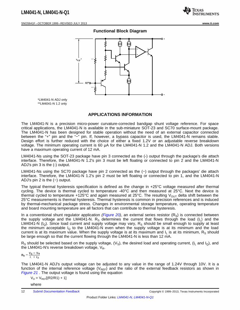
Functional Block Diagram
*LM4041-N ADJ only**LM4041-N 1.2 only
APPLICATIONS INFORMATION
The LM4041-N is a precision micro-power curvature-corrected bandgap shunt voltage reference. For spacecritical applications, the LM4041-N is available in the sub-miniature SOT-23 and SC70 surface-mount package.The LM4041-N has been designed for stable operation without the need of an external capacitor connectedbetween the “+” pin and the “−” pin. If, however, a bypass capacitor is used, the LM4041-N remains stable.Design effort is further reduced with the choice of either a fixed 1.2V or an adjustable reverse breakdownvoltage. The minimum operating current is 60 μA for the LM4041-N 1.2 and the LM4041-N ADJ. Both versionshave a maximum operating current of 12 mA.
LM4041-Ns using the SOT-23 package have pin 3 connected as the (-) output through the package's die attachinterface. Therefore, the LM4041-N 1.2's pin 3 must be left floating or connected to pin 2 and the LM4041-NADJ's pin 3 is the (-) output.
LM4041-Ns using the SC70 package have pin 2 connected as the (−) output through the packages' die attachinterface. Therefore, the LM4041-N 1.2's pin 2 must be left floating or connected to pin 1, and the LM4041-NADJ's pin 2 is the (−) output.
The typical thermal hysteresis specification is defined as the change in +25°C voltage measured after thermalcycling. The device is thermal cycled to temperature -40°C and then measured at 25°C. Next the device isthermal cycled to temperature +125°C and again measured at 25°C. The resulting VOUT delta shift between the25°C measurements is thermal hysteresis. Thermal hysteresis is common in precision references and is inducedby thermal-mechanical package stress. Changes in environmental storage temperature, operating temperatureand board mounting temperature are all factors that can contribute to thermal hysteresis.
In a conventional shunt regulator application (Figure 20), an external series resistor (RS) is connected betweenthe supply voltage and the LM4041-N. RS determines the current that flows through the load (IL) and theLM4041-N (IQ). Since load current and supply voltage may vary, RS should be small enough to supply at leastthe minimum acceptable IQ to the LM4041-N even when the supply voltage is at its minimum and the loadcurrent is at its maximum value. When the supply voltage is at its maximum and IL is at its minimum, RS shouldbe large enough so that the current flowing through the LM4041-N is less than 12 mA.
RS should be selected based on the supply voltage, (VS), the desired load and operating current, (IL and IQ), andthe LM4041-N's reverse breakdown voltage, VR.
The LM4041-N ADJ's output voltage can be adjusted to any value in the range of 1.24V through 10V. It is afunction of the internal reference voltage (VREF) and the ratio of the external feedback resistors as shown inFigure 21 . The output voltage is found using the equation
VO = VREF[(R2/R1) + 1]
where
12 Submit Documentation Feedback Copyright © 1999–2013, Texas Instruments Incorporated
Product Folder Links: LM4041-N, LM4041-N-Q1

LM4041-N, LM4041-N-Q1
www.ti.com SNOS641F –OCTOBER 1999–REVISED JULY 2013
• VO is the output voltage. The actual value of the internal VREF is a function of VO. The “corrected” VREF isdetermined by (1)
VREF = ΔVO (ΔVREF/ΔVO) + VY
where• VY = 1.240 V
and• ΔVO = (VO − VY) (2)
ΔVREF/ΔVO is found in the Electrical Characteristics and is typically −1.55 mV/V. You can get a more accurateindication of the output voltage by replacing the value of VREF in Equation 1 with the value found usingEquation 2.
Note that the actual output voltage can deviate from that predicted using the typical value of ΔVREF/ΔVO inEquation 2: for C-grade parts, the worst-case ΔVREF/ΔVO is −2.5 mV/V. For D-grade parts, the worst-caseΔVREF/ΔVO is −3.0 mV/V.
Typical Applications
Figure 20. Shunt Regulator
VO = VREF[(R2/R1) + 1]
Figure 21. Adjustable Shunt Regulator
Copyright © 1999–2013, Texas Instruments Incorporated Submit Documentation Feedback 13
Product Folder Links: LM4041-N, LM4041-N-Q1

LM4041-N, LM4041-N-Q1
SNOS641F –OCTOBER 1999–REVISED JULY 2013 www.ti.com
Figure 22. Bounded amplifier reduces saturation-induced delays and can prevent succeeding stagedamage. Nominal clamping voltage is ±VO (LM4041-N's reverse breakdown voltage) +2 diode VF.
Figure 23. Voltage Level Detector Figure 24. Voltage Level Detector
Figure 25. Fast Positive Clamp2.4V + VD1
14 Submit Documentation Feedback Copyright © 1999–2013, Texas Instruments Incorporated
Product Folder Links: LM4041-N, LM4041-N-Q1

LM4041-N, LM4041-N-Q1
www.ti.com SNOS641F –OCTOBER 1999–REVISED JULY 2013
Figure 26. Bidirectional Clamp ±2.4V
Figure 27. Bidirectional AdjustableClamp ±18V to ±2.4V
Figure 28. Bidirectional AdjustableClamp ±2.4V to ±6V
Copyright © 1999–2013, Texas Instruments Incorporated Submit Documentation Feedback 15
Product Folder Links: LM4041-N, LM4041-N-Q1

LM4041-N, LM4041-N-Q1
SNOS641F –OCTOBER 1999–REVISED JULY 2013 www.ti.com
Figure 29. Simple Floating Current Detector
*D1 can be any LED, VF = 1.5V to 2.2V at 3 mA. D1 may act as an indicator. D1 will be on if ITHRESHOLDfalls belowthe threshold current, except with I = 0.
Figure 30. Current Source
Figure 31. Precision Floating Current Detector
16 Submit Documentation Feedback Copyright © 1999–2013, Texas Instruments Incorporated
Product Folder Links: LM4041-N, LM4041-N-Q1

LM4041-N, LM4041-N-Q1
www.ti.com SNOS641F –OCTOBER 1999–REVISED JULY 2013
Figure 32. Precision 1 μA to 1 mA Current Sources
Copyright © 1999–2013, Texas Instruments Incorporated Submit Documentation Feedback 17
Product Folder Links: LM4041-N, LM4041-N-Q1

LM4041-N, LM4041-N-Q1
SNOS641F –OCTOBER 1999–REVISED JULY 2013 www.ti.com
REVISION HISTORY
Changes from Revision D (April 2013) to Revision E Page
• Changed layout of National Data Sheet to TI format .......................................................................................................... 16
18 Submit Documentation Feedback Copyright © 1999–2013, Texas Instruments Incorporated
Product Folder Links: LM4041-N, LM4041-N-Q1

PACKAGE OPTION ADDENDUM
www.ti.com 7-Oct-2013
Addendum-Page 1
PACKAGING INFORMATION
Orderable Device Status(1)
Package Type PackageDrawing
Pins PackageQty
Eco Plan(2)
Lead/Ball Finish MSL Peak Temp(3)
Op Temp (°C) Device Marking(4/5)
Samples
LM4041AIM3-1.2 ACTIVE SOT-23 DBZ 3 1000 TBD Call TI Call TI -40 to 85 R1A
LM4041AIM3-1.2/NOPB ACTIVE SOT-23 DBZ 3 1000 Green (RoHS& no Sb/Br)
CU SN Level-1-260C-UNLIM -40 to 85 R1A
LM4041AIM3X-1.2/NOPB ACTIVE SOT-23 DBZ 3 3000 Green (RoHS& no Sb/Br)
CU SN Level-1-260C-UNLIM -40 to 85 R1A
LM4041AIZ-1.2/NOPB ACTIVE TO-92 LP 3 1800 Green (RoHS& no Sb/Br)
N / A for Pkg Type -40 to 85 4041AIZ1.2
LM4041BIM3-1.2 ACTIVE SOT-23 DBZ 3 1000 TBD Call TI Call TI -40 to 85 R1B
LM4041BIM3-1.2/NOPB ACTIVE SOT-23 DBZ 3 1000 Green (RoHS& no Sb/Br)
CU SN Level-1-260C-UNLIM -40 to 85 R1B
LM4041BIM3X-1.2/NOPB ACTIVE SOT-23 DBZ 3 3000 Green (RoHS& no Sb/Br)
CU SN Level-1-260C-UNLIM -40 to 85 R1B
LM4041BIM7-1.2 ACTIVE SC70 DCK 5 1000 TBD Call TI Call TI -40 to 85 R1B
LM4041BIM7-1.2/NOPB ACTIVE SC70 DCK 5 1000 Green (RoHS& no Sb/Br)
CU SN Level-1-260C-UNLIM -40 to 85 R1B
LM4041BIM7X-1.2 ACTIVE SC70 DCK 5 3000 TBD Call TI Call TI -40 to 85 R1B
LM4041BIM7X-1.2/NOPB ACTIVE SC70 DCK 5 3000 Green (RoHS& no Sb/Br)
CU SN Level-1-260C-UNLIM -40 to 85 R1B
LM4041BIZ-1.2/NOPB ACTIVE TO-92 LP 3 1800 Green (RoHS& no Sb/Br)
N / A for Pkg Type -40 to 85 4041BIZ1.2
LM4041CEM3-1.2 ACTIVE SOT-23 DBZ 3 1000 TBD Call TI Call TI -40 to 125 R1C
LM4041CEM3-1.2/NOPB ACTIVE SOT-23 DBZ 3 1000 Green (RoHS& no Sb/Br)
CU SN Level-1-260C-UNLIM -40 to 125 R1C
LM4041CEM3-ADJ ACTIVE SOT-23 DBZ 3 1000 TBD Call TI Call TI -40 to 125 RAC
LM4041CEM3-ADJ/NOPB ACTIVE SOT-23 DBZ 3 1000 Green (RoHS& no Sb/Br)
CU SN Level-1-260C-UNLIM -40 to 125 RAC
LM4041CEM3X-1.2/NOPB ACTIVE SOT-23 DBZ 3 3000 Green (RoHS& no Sb/Br)
CU SN Level-1-260C-UNLIM -40 to 125 R1C
LM4041CEM3X-ADJ ACTIVE SOT-23 DBZ 3 3000 TBD Call TI Call TI -40 to 125 RAC

PACKAGE OPTION ADDENDUM
www.ti.com 7-Oct-2013
Addendum-Page 2
Orderable Device Status(1)
Package Type PackageDrawing
Pins PackageQty
Eco Plan(2)
Lead/Ball Finish MSL Peak Temp(3)
Op Temp (°C) Device Marking(4/5)
Samples
LM4041CEM3X-ADJ/NOPB ACTIVE SOT-23 DBZ 3 3000 Green (RoHS& no Sb/Br)
CU SN Level-1-260C-UNLIM -40 to 125 RAC
LM4041CIM3-1.2 ACTIVE SOT-23 DBZ 3 1000 TBD Call TI Call TI -40 to 85 R1C
LM4041CIM3-1.2/NOPB ACTIVE SOT-23 DBZ 3 1000 Green (RoHS& no Sb/Br)
CU SN Level-1-260C-UNLIM -40 to 85 R1C
LM4041CIM3-ADJ ACTIVE SOT-23 DBZ 3 1000 TBD Call TI Call TI -40 to 85 RAC
LM4041CIM3-ADJ/NOPB ACTIVE SOT-23 DBZ 3 1000 Green (RoHS& no Sb/Br)
CU SN Level-1-260C-UNLIM -40 to 85 RAC
LM4041CIM3X-1.2 ACTIVE SOT-23 DBZ 3 3000 TBD Call TI Call TI -40 to 85 R1C
LM4041CIM3X-1.2/NOPB ACTIVE SOT-23 DBZ 3 3000 Green (RoHS& no Sb/Br)
CU SN Level-1-260C-UNLIM -40 to 85 R1C
LM4041CIM3X-ADJ ACTIVE SOT-23 DBZ 3 3000 TBD Call TI Call TI -40 to 85 RAC
LM4041CIM3X-ADJ/NOPB ACTIVE SOT-23 DBZ 3 3000 Green (RoHS& no Sb/Br)
CU SN Level-1-260C-UNLIM -40 to 85 RAC
LM4041CIM7-1.2/NOPB ACTIVE SC70 DCK 5 1000 Green (RoHS& no Sb/Br)
CU SN Level-1-260C-UNLIM -40 to 85 R1C
LM4041CIM7-ADJ ACTIVE SC70 DCK 5 1000 TBD Call TI Call TI -40 to 85 RAC
LM4041CIM7-ADJ/NOPB ACTIVE SC70 DCK 5 1000 Green (RoHS& no Sb/Br)
CU SN Level-1-260C-UNLIM -40 to 85 RAC
LM4041CIM7X-1.2/NOPB ACTIVE SC70 DCK 5 3000 Green (RoHS& no Sb/Br)
CU SN Level-1-260C-UNLIM -40 to 85 R1C
LM4041CIM7X-ADJ ACTIVE SC70 DCK 5 3000 TBD Call TI Call TI -40 to 85 RAC
LM4041CIM7X-ADJ/NOPB ACTIVE SC70 DCK 5 3000 Green (RoHS& no Sb/Br)
CU SN Level-1-260C-UNLIM -40 to 85 RAC
LM4041CIZ-1.2/NOPB ACTIVE TO-92 LP 3 1800 Green (RoHS& no Sb/Br)
N / A for Pkg Type -40 to 85 4041CIZ1.2
LM4041CIZ-ADJ/NOPB ACTIVE TO-92 LP 3 1800 Green (RoHS& no Sb/Br)
N / A for Pkg Type -40 to 85 4041CIZADJ
LM4041DEM3-1.2/NOPB ACTIVE SOT-23 DBZ 3 1000 Green (RoHS& no Sb/Br)
CU SN Level-1-260C-UNLIM -40 to 125 R1D
LM4041DEM3-ADJ ACTIVE SOT-23 DBZ 3 1000 TBD Call TI Call TI -40 to 125 RAD

PACKAGE OPTION ADDENDUM
www.ti.com 7-Oct-2013
Addendum-Page 3
Orderable Device Status(1)
Package Type PackageDrawing
Pins PackageQty
Eco Plan(2)
Lead/Ball Finish MSL Peak Temp(3)
Op Temp (°C) Device Marking(4/5)
Samples
LM4041DEM3-ADJ/NOPB ACTIVE SOT-23 DBZ 3 1000 Green (RoHS& no Sb/Br)
CU SN Level-1-260C-UNLIM -40 to 125 RAD
LM4041DEM3X-1.2/NOPB ACTIVE SOT-23 DBZ 3 3000 Green (RoHS& no Sb/Br)
CU SN Level-1-260C-UNLIM -40 to 125 R1D
LM4041DEM3X-ADJ/NOPB ACTIVE SOT-23 DBZ 3 3000 Green (RoHS& no Sb/Br)
CU SN Level-1-260C-UNLIM -40 to 125 RAD
LM4041DIM3-1.2 ACTIVE SOT-23 DBZ 3 1000 TBD Call TI Call TI -40 to 85 R1D
LM4041DIM3-1.2/NOPB ACTIVE SOT-23 DBZ 3 1000 Green (RoHS& no Sb/Br)
CU SN Level-1-260C-UNLIM -40 to 85 R1D
LM4041DIM3-ADJ ACTIVE SOT-23 DBZ 3 1000 TBD Call TI Call TI -40 to 85 RAD
LM4041DIM3-ADJ/NOPB ACTIVE SOT-23 DBZ 3 1000 Green (RoHS& no Sb/Br)
CU SN Level-1-260C-UNLIM -40 to 85 RAD
LM4041DIM3X-1.2 ACTIVE SOT-23 DBZ 3 3000 TBD Call TI Call TI -40 to 85 R1D
LM4041DIM3X-1.2/NOPB ACTIVE SOT-23 DBZ 3 3000 Green (RoHS& no Sb/Br)
CU SN Level-1-260C-UNLIM -40 to 85 R1D
LM4041DIM3X-ADJ ACTIVE SOT-23 DBZ 3 3000 TBD Call TI Call TI -40 to 85 RAD
LM4041DIM3X-ADJ/NOPB ACTIVE SOT-23 DBZ 3 3000 Green (RoHS& no Sb/Br)
CU SN Level-1-260C-UNLIM -40 to 85 RAD
LM4041DIM7-1.2/NOPB ACTIVE SC70 DCK 5 1000 Green (RoHS& no Sb/Br)
CU SN Level-1-260C-UNLIM -40 to 85 R1D
LM4041DIM7-ADJ/NOPB ACTIVE SC70 DCK 5 1000 Green (RoHS& no Sb/Br)
CU SN Level-1-260C-UNLIM -40 to 85 RAD
LM4041DIM7X-1.2/NOPB ACTIVE SC70 DCK 5 3000 Green (RoHS& no Sb/Br)
CU SN Level-1-260C-UNLIM -40 to 85 R1D
LM4041DIM7X-ADJ/NOPB ACTIVE SC70 DCK 5 3000 Green (RoHS& no Sb/Br)
CU SN Level-1-260C-UNLIM -40 to 85 RAD
LM4041DIZ-1.2/NOPB ACTIVE TO-92 LP 3 1800 Green (RoHS& no Sb/Br)
N / A for Pkg Type -40 to 85 4041DIZ1.2
LM4041DIZ-ADJ/LFT1 ACTIVE TO-92 LP 3 2000 Green (RoHS& no Sb/Br)
N / A for Pkg Type (4040D ~ 4041D)IZADJ
LM4041DIZ-ADJ/NOPB ACTIVE TO-92 LP 3 1800 Green (RoHS& no Sb/Br)
N / A for Pkg Type -40 to 85 4041DIZADJ
LM4041EEM3-1.2 ACTIVE SOT-23 DBZ 3 1000 TBD Call TI Call TI -40 to 125 R1E

PACKAGE OPTION ADDENDUM
www.ti.com 7-Oct-2013
Addendum-Page 4
Orderable Device Status(1)
Package Type PackageDrawing
Pins PackageQty
Eco Plan(2)
Lead/Ball Finish MSL Peak Temp(3)
Op Temp (°C) Device Marking(4/5)
Samples
LM4041EEM3-1.2/NOPB ACTIVE SOT-23 DBZ 3 1000 Green (RoHS& no Sb/Br)
CU SN Level-1-260C-UNLIM -40 to 125 R1E
LM4041EEM3X-1.2 ACTIVE SOT-23 DBZ 3 3000 TBD Call TI Call TI -40 to 125 R1E
LM4041EEM3X-1.2/NOPB ACTIVE SOT-23 DBZ 3 3000 Green (RoHS& no Sb/Br)
CU SN Level-1-260C-UNLIM -40 to 125 R1E
LM4041EIM3-1.2 ACTIVE SOT-23 DBZ 3 1000 TBD Call TI Call TI -40 to 85 R1E
LM4041EIM3-1.2/NOPB ACTIVE SOT-23 DBZ 3 1000 Green (RoHS& no Sb/Br)
CU SN Level-1-260C-UNLIM -40 to 85 R1E
LM4041EIM3X-1.2 ACTIVE SOT-23 DBZ 3 3000 TBD Call TI Call TI -40 to 85 R1E
LM4041EIM3X-1.2/NOPB ACTIVE SOT-23 DBZ 3 3000 Green (RoHS& no Sb/Br)
CU SN Level-1-260C-UNLIM -40 to 85 R1E
LM4041EIM7-1.2 ACTIVE SC70 DCK 5 1000 TBD Call TI Call TI -40 to 85 R1E
LM4041EIM7-1.2/NOPB ACTIVE SC70 DCK 5 1000 Green (RoHS& no Sb/Br)
CU SN Level-1-260C-UNLIM -40 to 85 R1E
LM4041EIM7X-1.2/NOPB ACTIVE SC70 DCK 5 3000 Green (RoHS& no Sb/Br)
CU SN Level-1-260C-UNLIM -40 to 85 R1E
LM4041QAIM3-1.2/NO PREVIEW SOT-23 DBZ 3 1000 Green (RoHS& no Sb/Br)
CU SN Level-1-260C-UNLIM -40 to 85 RQA
LM4041QAIM3X-1.2NO PREVIEW SOT-23 DBZ 3 3000 Green (RoHS& no Sb/Br)
CU SN Level-1-260C-UNLIM -40 to 85 RQA
LM4041QBIM3-1.2/NO PREVIEW SOT-23 DBZ 3 1000 Green (RoHS& no Sb/Br)
CU SN Level-1-260C-UNLIM -40 to 85 RQB
LM4041QBIM3X-1.2NO PREVIEW SOT-23 DBZ 3 3000 TBD Call TI Call TI -40 to 85 RQB
LM4041QCEM3-1.2NO ACTIVE SOT-23 DBZ 3 1000 Green (RoHS& no Sb/Br)
CU SN Level-1-260C-UNLIM -40 to 125 RQC
LM4041QCEM3-ADJ/NO PREVIEW SOT-23 DBZ 3 1000 TBD Call TI Call TI -40 to 125 RZC
LM4041QCEM3X-1.2NO ACTIVE SOT-23 DBZ 3 3000 Green (RoHS& no Sb/Br)
CU SN Level-1-260C-UNLIM -40 to 125 RQC
LM4041QCEM3X-ADJNO PREVIEW SOT-23 DBZ 3 3000 TBD Call TI Call TI -40 to 125 RZC
LM4041QCIM3-1.2/NO PREVIEW SOT-23 DBZ 3 1000 Green (RoHS& no Sb/Br)
CU SN Level-1-260C-UNLIM -40 to 125 RQC
LM4041QCIM3-ADJ/NO PREVIEW SOT-23 DBZ 3 1000 TBD Call TI Call TI -40 to 125 RZC
LM4041QCIM3X-1.2NO PREVIEW SOT-23 DBZ 3 3000 TBD Call TI Call TI -40 to 125 RQC

PACKAGE OPTION ADDENDUM
www.ti.com 7-Oct-2013
Addendum-Page 5
Orderable Device Status(1)
Package Type PackageDrawing
Pins PackageQty
Eco Plan(2)
Lead/Ball Finish MSL Peak Temp(3)
Op Temp (°C) Device Marking(4/5)
Samples
LM4041QCIM3X-ADJNO PREVIEW SOT-23 DBZ 3 3000 TBD Call TI Call TI -40 to 125 RZC
LM4041QDEM3-1.2/NO PREVIEW SOT-23 DBZ 3 1000 TBD Call TI Call TI -40 to 125 RQD
LM4041QDEM3-ADJ/NO PREVIEW SOT-23 DBZ 3 1000 TBD Call TI Call TI -40 to 125 RZD
LM4041QDEM3X-1.2NO PREVIEW SOT-23 DBZ 3 3000 TBD Call TI Call TI -40 to 125 RQD
LM4041QDEM3X-ADJNO PREVIEW SOT-23 DBZ 3 3000 TBD Call TI Call TI -40 to 125 RZD
LM4041QDIM3-1.2/NO PREVIEW SOT-23 DBZ 3 1000 Green (RoHS& no Sb/Br)
CU SN Level-1-260C-UNLIM -40 to 125 RQD
LM4041QDIM3-ADJ/NO PREVIEW SOT-23 DBZ 3 1000 TBD Call TI Call TI -40 to 125 RZD
LM4041QDIM3X-1.2NO PREVIEW SOT-23 DBZ 3 3000 Green (RoHS& no Sb/Br)
CU SN Level-1-260C-UNLIM -40 to 125 RQD
LM4041QDIM3X-ADJNO PREVIEW SOT-23 DBZ 3 3000 TBD Call TI Call TI -40 to 125 RZD
LM4041QEEM3-1.2/NO ACTIVE SOT-23 DBZ 3 1000 Green (RoHS& no Sb/Br)
CU SN Level-1-260C-UNLIM -40 to 125 RQE
LM4041QEEM3X-1.2NO ACTIVE SOT-23 DBZ 3 3000 TBD Call TI Call TI -40 to 125 RQE
LM4041QEIM3-1.2/NO PREVIEW SOT-23 DBZ 3 1000 Green (RoHS& no Sb/Br)
CU SN Level-1-260C-UNLIM -40 to 125 RQE
LM4041QEIM3X-1.2NO PREVIEW SOT-23 DBZ 3 3000 TBD Call TI Call TI -40 to 125 RQE (1) The marketing status values are defined as follows:ACTIVE: Product device recommended for new designs.LIFEBUY: TI has announced that the device will be discontinued, and a lifetime-buy period is in effect.NRND: Not recommended for new designs. Device is in production to support existing customers, but TI does not recommend using this part in a new design.PREVIEW: Device has been announced but is not in production. Samples may or may not be available.OBSOLETE: TI has discontinued the production of the device.
(2) Eco Plan - The planned eco-friendly classification: Pb-Free (RoHS), Pb-Free (RoHS Exempt), or Green (RoHS & no Sb/Br) - please check http://www.ti.com/productcontent for the latest availabilityinformation and additional product content details.TBD: The Pb-Free/Green conversion plan has not been defined.Pb-Free (RoHS): TI's terms "Lead-Free" or "Pb-Free" mean semiconductor products that are compatible with the current RoHS requirements for all 6 substances, including the requirement thatlead not exceed 0.1% by weight in homogeneous materials. Where designed to be soldered at high temperatures, TI Pb-Free products are suitable for use in specified lead-free processes.Pb-Free (RoHS Exempt): This component has a RoHS exemption for either 1) lead-based flip-chip solder bumps used between the die and package, or 2) lead-based die adhesive used betweenthe die and leadframe. The component is otherwise considered Pb-Free (RoHS compatible) as defined above.Green (RoHS & no Sb/Br): TI defines "Green" to mean Pb-Free (RoHS compatible), and free of Bromine (Br) and Antimony (Sb) based flame retardants (Br or Sb do not exceed 0.1% by weightin homogeneous material)
(3) MSL, Peak Temp. -- The Moisture Sensitivity Level rating according to the JEDEC industry standard classifications, and peak solder temperature.

PACKAGE OPTION ADDENDUM
www.ti.com 7-Oct-2013
Addendum-Page 6
(4) There may be additional marking, which relates to the logo, the lot trace code information, or the environmental category on the device.
(5) Multiple Device Markings will be inside parentheses. Only one Device Marking contained in parentheses and separated by a "~" will appear on a device. If a line is indented then it is a continuationof the previous line and the two combined represent the entire Device Marking for that device.
Important Information and Disclaimer:The information provided on this page represents TI's knowledge and belief as of the date that it is provided. TI bases its knowledge and belief on informationprovided by third parties, and makes no representation or warranty as to the accuracy of such information. Efforts are underway to better integrate information from third parties. TI has taken andcontinues to take reasonable steps to provide representative and accurate information but may not have conducted destructive testing or chemical analysis on incoming materials and chemicals.TI and TI suppliers consider certain information to be proprietary, and thus CAS numbers and other limited information may not be available for release.
In no event shall TI's liability arising out of such information exceed the total purchase price of the TI part(s) at issue in this document sold by TI to Customer on an annual basis.
OTHER QUALIFIED VERSIONS OF LM4041-N, LM4041-N-Q1 :
• Catalog: LM4041-N
• Automotive: LM4041-N-Q1
NOTE: Qualified Version Definitions:
• Catalog - TI's standard catalog product
• Automotive - Q100 devices qualified for high-reliability automotive applications targeting zero defects

TAPE AND REEL INFORMATION
*All dimensions are nominal
Device PackageType
PackageDrawing
Pins SPQ ReelDiameter
(mm)
ReelWidth
W1 (mm)
A0(mm)
B0(mm)
K0(mm)
P1(mm)
W(mm)
Pin1Quadrant
LM4041AIM3-1.2 SOT-23 DBZ 3 1000 178.0 8.4 3.3 2.9 1.22 4.0 8.0 Q3
LM4041AIM3-1.2/NOPB SOT-23 DBZ 3 1000 178.0 8.4 3.3 2.9 1.22 4.0 8.0 Q3
LM4041AIM3X-1.2/NOPB SOT-23 DBZ 3 3000 178.0 8.4 3.3 2.9 1.22 4.0 8.0 Q3
LM4041BIM3-1.2 SOT-23 DBZ 3 1000 178.0 8.4 3.3 2.9 1.22 4.0 8.0 Q3
LM4041BIM3-1.2/NOPB SOT-23 DBZ 3 1000 178.0 8.4 3.3 2.9 1.22 4.0 8.0 Q3
LM4041BIM3X-1.2/NOPB SOT-23 DBZ 3 3000 178.0 8.4 3.3 2.9 1.22 4.0 8.0 Q3
LM4041BIM7-1.2 SC70 DCK 5 1000 178.0 8.4 2.25 2.45 1.2 4.0 8.0 Q3
LM4041BIM7-1.2/NOPB SC70 DCK 5 1000 178.0 8.4 2.25 2.45 1.2 4.0 8.0 Q3
LM4041BIM7X-1.2 SC70 DCK 5 3000 178.0 8.4 2.25 2.45 1.2 4.0 8.0 Q3
LM4041BIM7X-1.2/NOPB SC70 DCK 5 3000 178.0 8.4 2.25 2.45 1.2 4.0 8.0 Q3
LM4041CEM3-1.2 SOT-23 DBZ 3 1000 178.0 8.4 3.3 2.9 1.22 4.0 8.0 Q3
LM4041CEM3-1.2/NOPB SOT-23 DBZ 3 1000 178.0 8.4 3.3 2.9 1.22 4.0 8.0 Q3
LM4041CEM3-ADJ SOT-23 DBZ 3 1000 178.0 8.4 3.3 2.9 1.22 4.0 8.0 Q3
LM4041CEM3-ADJ/NOPB SOT-23 DBZ 3 1000 178.0 8.4 3.3 2.9 1.22 4.0 8.0 Q3
LM4041CEM3X-1.2/NOPB SOT-23 DBZ 3 3000 178.0 8.4 3.3 2.9 1.22 4.0 8.0 Q3
LM4041CEM3X-ADJ SOT-23 DBZ 3 3000 178.0 8.4 3.3 2.9 1.22 4.0 8.0 Q3
LM4041CEM3X-ADJ/NOPB
SOT-23 DBZ 3 3000 178.0 8.4 3.3 2.9 1.22 4.0 8.0 Q3
PACKAGE MATERIALS INFORMATION
www.ti.com 23-Sep-2013
Pack Materials-Page 1

Device PackageType
PackageDrawing
Pins SPQ ReelDiameter
(mm)
ReelWidth
W1 (mm)
A0(mm)
B0(mm)
K0(mm)
P1(mm)
W(mm)
Pin1Quadrant
LM4041CIM3-1.2 SOT-23 DBZ 3 1000 178.0 8.4 3.3 2.9 1.22 4.0 8.0 Q3
LM4041CIM3-1.2/NOPB SOT-23 DBZ 3 1000 178.0 8.4 3.3 2.9 1.22 4.0 8.0 Q3
LM4041CIM3-ADJ SOT-23 DBZ 3 1000 178.0 8.4 3.3 2.9 1.22 4.0 8.0 Q3
LM4041CIM3-ADJ/NOPB SOT-23 DBZ 3 1000 178.0 8.4 3.3 2.9 1.22 4.0 8.0 Q3
LM4041CIM3X-1.2 SOT-23 DBZ 3 3000 178.0 8.4 3.3 2.9 1.22 4.0 8.0 Q3
LM4041CIM3X-1.2/NOPB SOT-23 DBZ 3 3000 178.0 8.4 3.3 2.9 1.22 4.0 8.0 Q3
LM4041CIM3X-ADJ SOT-23 DBZ 3 3000 178.0 8.4 3.3 2.9 1.22 4.0 8.0 Q3
LM4041CIM3X-ADJ/NOPB
SOT-23 DBZ 3 3000 178.0 8.4 3.3 2.9 1.22 4.0 8.0 Q3
LM4041CIM7-1.2/NOPB SC70 DCK 5 1000 178.0 8.4 2.25 2.45 1.2 4.0 8.0 Q3
LM4041CIM7-ADJ SC70 DCK 5 1000 178.0 8.4 2.25 2.45 1.2 4.0 8.0 Q3
LM4041CIM7-ADJ/NOPB SC70 DCK 5 1000 178.0 8.4 2.25 2.45 1.2 4.0 8.0 Q3
LM4041CIM7X-1.2/NOPB SC70 DCK 5 3000 178.0 8.4 2.25 2.45 1.2 4.0 8.0 Q3
LM4041CIM7X-ADJ SC70 DCK 5 3000 178.0 8.4 2.25 2.45 1.2 4.0 8.0 Q3
LM4041CIM7X-ADJ/NOPB
SC70 DCK 5 3000 178.0 8.4 2.25 2.45 1.2 4.0 8.0 Q3
LM4041DEM3-1.2/NOPB SOT-23 DBZ 3 1000 178.0 8.4 3.3 2.9 1.22 4.0 8.0 Q3
LM4041DEM3-ADJ SOT-23 DBZ 3 1000 178.0 8.4 3.3 2.9 1.22 4.0 8.0 Q3
LM4041DEM3-ADJ/NOPB SOT-23 DBZ 3 1000 178.0 8.4 3.3 2.9 1.22 4.0 8.0 Q3
LM4041DEM3X-1.2/NOPB SOT-23 DBZ 3 3000 178.0 8.4 3.3 2.9 1.22 4.0 8.0 Q3
LM4041DEM3X-ADJ/NOPB
SOT-23 DBZ 3 3000 178.0 8.4 3.3 2.9 1.22 4.0 8.0 Q3
LM4041DIM3-1.2 SOT-23 DBZ 3 1000 178.0 8.4 3.3 2.9 1.22 4.0 8.0 Q3
LM4041DIM3-1.2/NOPB SOT-23 DBZ 3 1000 178.0 8.4 3.3 2.9 1.22 4.0 8.0 Q3
LM4041DIM3-ADJ SOT-23 DBZ 3 1000 178.0 8.4 3.3 2.9 1.22 4.0 8.0 Q3
LM4041DIM3-ADJ/NOPB SOT-23 DBZ 3 1000 178.0 8.4 3.3 2.9 1.22 4.0 8.0 Q3
LM4041DIM3X-1.2 SOT-23 DBZ 3 3000 178.0 8.4 3.3 2.9 1.22 4.0 8.0 Q3
LM4041DIM3X-1.2/NOPB SOT-23 DBZ 3 3000 178.0 8.4 3.3 2.9 1.22 4.0 8.0 Q3
LM4041DIM3X-ADJ SOT-23 DBZ 3 3000 178.0 8.4 3.3 2.9 1.22 4.0 8.0 Q3
LM4041DIM3X-ADJ/NOPB
SOT-23 DBZ 3 3000 178.0 8.4 3.3 2.9 1.22 4.0 8.0 Q3
LM4041DIM7-1.2/NOPB SC70 DCK 5 1000 178.0 8.4 2.25 2.45 1.2 4.0 8.0 Q3
LM4041DIM7-ADJ/NOPB SC70 DCK 5 1000 178.0 8.4 2.25 2.45 1.2 4.0 8.0 Q3
LM4041DIM7X-1.2/NOPB SC70 DCK 5 3000 178.0 8.4 2.25 2.45 1.2 4.0 8.0 Q3
LM4041DIM7X-ADJ/NOPB
SC70 DCK 5 3000 178.0 8.4 2.25 2.45 1.2 4.0 8.0 Q3
LM4041EEM3-1.2 SOT-23 DBZ 3 1000 178.0 8.4 3.3 2.9 1.22 4.0 8.0 Q3
LM4041EEM3-1.2/NOPB SOT-23 DBZ 3 1000 178.0 8.4 3.3 2.9 1.22 4.0 8.0 Q3
LM4041EEM3X-1.2 SOT-23 DBZ 3 3000 178.0 8.4 3.3 2.9 1.22 4.0 8.0 Q3
LM4041EEM3X-1.2/NOPB SOT-23 DBZ 3 3000 178.0 8.4 3.3 2.9 1.22 4.0 8.0 Q3
LM4041EIM3-1.2 SOT-23 DBZ 3 1000 178.0 8.4 3.3 2.9 1.22 4.0 8.0 Q3
LM4041EIM3-1.2/NOPB SOT-23 DBZ 3 1000 178.0 8.4 3.3 2.9 1.22 4.0 8.0 Q3
LM4041EIM3X-1.2 SOT-23 DBZ 3 3000 178.0 8.4 3.3 2.9 1.22 4.0 8.0 Q3
LM4041EIM3X-1.2/NOPB SOT-23 DBZ 3 3000 178.0 8.4 3.3 2.9 1.22 4.0 8.0 Q3
PACKAGE MATERIALS INFORMATION
www.ti.com 23-Sep-2013
Pack Materials-Page 2

Device PackageType
PackageDrawing
Pins SPQ ReelDiameter
(mm)
ReelWidth
W1 (mm)
A0(mm)
B0(mm)
K0(mm)
P1(mm)
W(mm)
Pin1Quadrant
LM4041EIM7-1.2 SC70 DCK 5 1000 178.0 8.4 2.25 2.45 1.2 4.0 8.0 Q3
LM4041EIM7-1.2/NOPB SC70 DCK 5 1000 178.0 8.4 2.25 2.45 1.2 4.0 8.0 Q3
LM4041EIM7X-1.2/NOPB SC70 DCK 5 3000 178.0 8.4 2.25 2.45 1.2 4.0 8.0 Q3
*All dimensions are nominal
Device Package Type Package Drawing Pins SPQ Length (mm) Width (mm) Height (mm)
LM4041AIM3-1.2 SOT-23 DBZ 3 1000 210.0 185.0 35.0
LM4041AIM3-1.2/NOPB SOT-23 DBZ 3 1000 210.0 185.0 35.0
LM4041AIM3X-1.2/NOPB SOT-23 DBZ 3 3000 210.0 185.0 35.0
LM4041BIM3-1.2 SOT-23 DBZ 3 1000 210.0 185.0 35.0
LM4041BIM3-1.2/NOPB SOT-23 DBZ 3 1000 210.0 185.0 35.0
LM4041BIM3X-1.2/NOPB SOT-23 DBZ 3 3000 210.0 185.0 35.0
LM4041BIM7-1.2 SC70 DCK 5 1000 210.0 185.0 35.0
LM4041BIM7-1.2/NOPB SC70 DCK 5 1000 210.0 185.0 35.0
LM4041BIM7X-1.2 SC70 DCK 5 3000 210.0 185.0 35.0
LM4041BIM7X-1.2/NOPB SC70 DCK 5 3000 210.0 185.0 35.0
LM4041CEM3-1.2 SOT-23 DBZ 3 1000 210.0 185.0 35.0
LM4041CEM3-1.2/NOPB SOT-23 DBZ 3 1000 210.0 185.0 35.0
LM4041CEM3-ADJ SOT-23 DBZ 3 1000 210.0 185.0 35.0
LM4041CEM3-ADJ/NOPB SOT-23 DBZ 3 1000 210.0 185.0 35.0
PACKAGE MATERIALS INFORMATION
www.ti.com 23-Sep-2013
Pack Materials-Page 3

Device Package Type Package Drawing Pins SPQ Length (mm) Width (mm) Height (mm)
LM4041CEM3X-1.2/NOPB SOT-23 DBZ 3 3000 210.0 185.0 35.0
LM4041CEM3X-ADJ SOT-23 DBZ 3 3000 210.0 185.0 35.0
LM4041CEM3X-ADJ/NOPB
SOT-23 DBZ 3 3000 210.0 185.0 35.0
LM4041CIM3-1.2 SOT-23 DBZ 3 1000 210.0 185.0 35.0
LM4041CIM3-1.2/NOPB SOT-23 DBZ 3 1000 210.0 185.0 35.0
LM4041CIM3-ADJ SOT-23 DBZ 3 1000 210.0 185.0 35.0
LM4041CIM3-ADJ/NOPB SOT-23 DBZ 3 1000 210.0 185.0 35.0
LM4041CIM3X-1.2 SOT-23 DBZ 3 3000 210.0 185.0 35.0
LM4041CIM3X-1.2/NOPB SOT-23 DBZ 3 3000 210.0 185.0 35.0
LM4041CIM3X-ADJ SOT-23 DBZ 3 3000 210.0 185.0 35.0
LM4041CIM3X-ADJ/NOPB SOT-23 DBZ 3 3000 210.0 185.0 35.0
LM4041CIM7-1.2/NOPB SC70 DCK 5 1000 210.0 185.0 35.0
LM4041CIM7-ADJ SC70 DCK 5 1000 210.0 185.0 35.0
LM4041CIM7-ADJ/NOPB SC70 DCK 5 1000 210.0 185.0 35.0
LM4041CIM7X-1.2/NOPB SC70 DCK 5 3000 210.0 185.0 35.0
LM4041CIM7X-ADJ SC70 DCK 5 3000 210.0 185.0 35.0
LM4041CIM7X-ADJ/NOPB SC70 DCK 5 3000 210.0 185.0 35.0
LM4041DEM3-1.2/NOPB SOT-23 DBZ 3 1000 210.0 185.0 35.0
LM4041DEM3-ADJ SOT-23 DBZ 3 1000 210.0 185.0 35.0
LM4041DEM3-ADJ/NOPB SOT-23 DBZ 3 1000 210.0 185.0 35.0
LM4041DEM3X-1.2/NOPB SOT-23 DBZ 3 3000 210.0 185.0 35.0
LM4041DEM3X-ADJ/NOPB
SOT-23 DBZ 3 3000 210.0 185.0 35.0
LM4041DIM3-1.2 SOT-23 DBZ 3 1000 210.0 185.0 35.0
LM4041DIM3-1.2/NOPB SOT-23 DBZ 3 1000 210.0 185.0 35.0
LM4041DIM3-ADJ SOT-23 DBZ 3 1000 210.0 185.0 35.0
LM4041DIM3-ADJ/NOPB SOT-23 DBZ 3 1000 210.0 185.0 35.0
LM4041DIM3X-1.2 SOT-23 DBZ 3 3000 210.0 185.0 35.0
LM4041DIM3X-1.2/NOPB SOT-23 DBZ 3 3000 210.0 185.0 35.0
LM4041DIM3X-ADJ SOT-23 DBZ 3 3000 210.0 185.0 35.0
LM4041DIM3X-ADJ/NOPB SOT-23 DBZ 3 3000 210.0 185.0 35.0
LM4041DIM7-1.2/NOPB SC70 DCK 5 1000 210.0 185.0 35.0
LM4041DIM7-ADJ/NOPB SC70 DCK 5 1000 210.0 185.0 35.0
LM4041DIM7X-1.2/NOPB SC70 DCK 5 3000 210.0 185.0 35.0
LM4041DIM7X-ADJ/NOPB SC70 DCK 5 3000 210.0 185.0 35.0
LM4041EEM3-1.2 SOT-23 DBZ 3 1000 210.0 185.0 35.0
LM4041EEM3-1.2/NOPB SOT-23 DBZ 3 1000 210.0 185.0 35.0
LM4041EEM3X-1.2 SOT-23 DBZ 3 3000 210.0 185.0 35.0
LM4041EEM3X-1.2/NOPB SOT-23 DBZ 3 3000 210.0 185.0 35.0
LM4041EIM3-1.2 SOT-23 DBZ 3 1000 210.0 185.0 35.0
LM4041EIM3-1.2/NOPB SOT-23 DBZ 3 1000 210.0 185.0 35.0
LM4041EIM3X-1.2 SOT-23 DBZ 3 3000 210.0 185.0 35.0
LM4041EIM3X-1.2/NOPB SOT-23 DBZ 3 3000 210.0 185.0 35.0
PACKAGE MATERIALS INFORMATION
www.ti.com 23-Sep-2013
Pack Materials-Page 4

Device Package Type Package Drawing Pins SPQ Length (mm) Width (mm) Height (mm)
LM4041EIM7-1.2 SC70 DCK 5 1000 210.0 185.0 35.0
LM4041EIM7-1.2/NOPB SC70 DCK 5 1000 210.0 185.0 35.0
LM4041EIM7X-1.2/NOPB SC70 DCK 5 3000 210.0 185.0 35.0
PACKAGE MATERIALS INFORMATION
www.ti.com 23-Sep-2013
Pack Materials-Page 5


IMPORTANT NOTICE
Texas Instruments Incorporated and its subsidiaries (TI) reserve the right to make corrections, enhancements, improvements and otherchanges to its semiconductor products and services per JESD46, latest issue, and to discontinue any product or service per JESD48, latestissue. Buyers should obtain the latest relevant information before placing orders and should verify that such information is current andcomplete. All semiconductor products (also referred to herein as “components”) are sold subject to TI’s terms and conditions of salesupplied at the time of order acknowledgment.
TI warrants performance of its components to the specifications applicable at the time of sale, in accordance with the warranty in TI’s termsand conditions of sale of semiconductor products. Testing and other quality control techniques are used to the extent TI deems necessaryto support this warranty. Except where mandated by applicable law, testing of all parameters of each component is not necessarilyperformed.
TI assumes no liability for applications assistance or the design of Buyers’ products. Buyers are responsible for their products andapplications using TI components. To minimize the risks associated with Buyers’ products and applications, Buyers should provideadequate design and operating safeguards.
TI does not warrant or represent that any license, either express or implied, is granted under any patent right, copyright, mask work right, orother intellectual property right relating to any combination, machine, or process in which TI components or services are used. Informationpublished by TI regarding third-party products or services does not constitute a license to use such products or services or a warranty orendorsement thereof. Use of such information may require a license from a third party under the patents or other intellectual property of thethird party, or a license from TI under the patents or other intellectual property of TI.
Reproduction of significant portions of TI information in TI data books or data sheets is permissible only if reproduction is without alterationand is accompanied by all associated warranties, conditions, limitations, and notices. TI is not responsible or liable for such altereddocumentation. Information of third parties may be subject to additional restrictions.
Resale of TI components or services with statements different from or beyond the parameters stated by TI for that component or servicevoids all express and any implied warranties for the associated TI component or service and is an unfair and deceptive business practice.TI is not responsible or liable for any such statements.
Buyer acknowledges and agrees that it is solely responsible for compliance with all legal, regulatory and safety-related requirementsconcerning its products, and any use of TI components in its applications, notwithstanding any applications-related information or supportthat may be provided by TI. Buyer represents and agrees that it has all the necessary expertise to create and implement safeguards whichanticipate dangerous consequences of failures, monitor failures and their consequences, lessen the likelihood of failures that might causeharm and take appropriate remedial actions. Buyer will fully indemnify TI and its representatives against any damages arising out of the useof any TI components in safety-critical applications.
In some cases, TI components may be promoted specifically to facilitate safety-related applications. With such components, TI’s goal is tohelp enable customers to design and create their own end-product solutions that meet applicable functional safety standards andrequirements. Nonetheless, such components are subject to these terms.
No TI components are authorized for use in FDA Class III (or similar life-critical medical equipment) unless authorized officers of the partieshave executed a special agreement specifically governing such use.
Only those TI components which TI has specifically designated as military grade or “enhanced plastic” are designed and intended for use inmilitary/aerospace applications or environments. Buyer acknowledges and agrees that any military or aerospace use of TI componentswhich have not been so designated is solely at the Buyer's risk, and that Buyer is solely responsible for compliance with all legal andregulatory requirements in connection with such use.
TI has specifically designated certain components as meeting ISO/TS16949 requirements, mainly for automotive use. In any case of use ofnon-designated products, TI will not be responsible for any failure to meet ISO/TS16949.
Products Applications
Audio www.ti.com/audio Automotive and Transportation www.ti.com/automotive
Amplifiers amplifier.ti.com Communications and Telecom www.ti.com/communications
Data Converters dataconverter.ti.com Computers and Peripherals www.ti.com/computers
DLP® Products www.dlp.com Consumer Electronics www.ti.com/consumer-apps
DSP dsp.ti.com Energy and Lighting www.ti.com/energy
Clocks and Timers www.ti.com/clocks Industrial www.ti.com/industrial
Interface interface.ti.com Medical www.ti.com/medical
Logic logic.ti.com Security www.ti.com/security
Power Mgmt power.ti.com Space, Avionics and Defense www.ti.com/space-avionics-defense
Microcontrollers microcontroller.ti.com Video and Imaging www.ti.com/video
RFID www.ti-rfid.com
OMAP Applications Processors www.ti.com/omap TI E2E Community e2e.ti.com
Wireless Connectivity www.ti.com/wirelessconnectivity
Mailing Address: Texas Instruments, Post Office Box 655303, Dallas, Texas 75265Copyright © 2013, Texas Instruments Incorporated