logic design using memristors: an emerging …...logic design using memristors: an emerging...
TRANSCRIPT

Logic Design using Memristors:An Emerging Technology
(Embedded Tutorial)
Saeideh Shirinzadeh∗ Kamalika Datta† Rolf Drechsler∗‡∗Department of Mathematics and Computer Science, University of Bremen, Bremen, Germany
†Department of Computer Science and Engineering, National Institute of Technology Meghalaya, India‡Cyber-Physical Systems, DFKI GmbH, Bremen, Germany
Email: [email protected], {s.shirinzadeh,drechsler}@uni-bremen.de
Abstract—This paper provides an introduction to memristor,which is considered as the fourth circuit element along withresistor, inductor and capacitor. Memristors possess some uniqueproperties, i.e. it can change the resistance under voltage controland can retain its value even after the voltage is withdrawn.Another property of memristors is their small feature size whichmakes them useful for design of ultra-compact memory systems.In addition, the resistive switching property of memristors allowsto execute logic primitives and thus can also be used for imple-menting logic functions using various logic design styles studiedin this paper. The paper also discusses memristor fabrication,circuit models, methods for implementing logic functions, andthe various computing methodologies that can be used viz. near-memory computing and in-memory computing.
Index Terms—Memristor, IMPLY, MAGIC, in-memory com-puting, logic synthesis
I. INTRODUCTION
The memristor has been considered by scientists as thefourth fundamental circuit element after resistor, capacitorand inductor. Chua predicted the existience of memristors in1971 [1], as a circuit element that directly relates magnetic fluxand charge. The current-voltage characteristic of a memristorexhibits a pinched hysteresis loop, that allows switching ofresistive states. In 2008, a group of researchers in the HPLabs were successful in fabricating a device [2] using a TiO2material doped with oxygen vacancy, which has similar resistiveswitching properties. The memristor has the unique propertythat its resistance value can be changed by applying a suitablevoltage across it, and the resistance value does not change evenif the voltage is withdrawn. Subsequently, various other researchgroups successfully demonstrated the fabrication of deviceswith similar properties [3], [4]. One of the biggest advantagesthat memristors offer is their extremely small size as comparedto conventional MOS transistors. In fact, a memristor can befabricated with feature size as small as 9 nm2 [5].
Due to their ability to memorize past states, memristorscan be used to build high capacity non-volatile resistivememory systems. Because of their extremely small sizes andregular structure, they can be very conveniently fabricated ina crossbar array. Over and above applications of memristorsin memory systems, several works have been reported wherethey have been used for the implementation of logic functionsand interconnections. There are several design styles for
implementing logic functions using memristors, two of whichare briefly stated below.
a) In memristor IMPLY logic [6], memristors can be usedto realize the material implication operation (A→ B =A′ + B). The initial values of A and B, and also theresult are stored as resistance values in memristors. Toimplement a complex function, several IMPLY operationsmay need to be done in a particular sequence.
b) The MAGIC design style [7] uses only memristors toimplement logic gates, where the inputs are appliedas resistance values. MAGIC gate realizations can bemapped to crossbar arrays, and offer flexibility andscalability.
c) Recently, a number of works have been carried outon memristor crossbar arrays [8], [9], where a two-dimensional grid of memristors is created. By suitablyinitializing the memristors to known states, and applyingsuitable voltages to the rows and columns, logic functionscan be computed as determined by the current flowingthrough the array. One problem with this approach isthe existence of sneak paths in the crossbar, throughwhich unwanted currents may start flowing resulting inerroneous output. However, because of the highly densenature of the crossbar, this approach holds great potential.
II. MEMRISTOR: FABRICATION AND MODELING
The memristor represents a non-linear relationship betweenelectrical charge and magnetic flux [1], as shown in Fig. 1(a).In 2008, Strukov et al. fabricated a memristor device at HPLab. They used a TiO2 material sandwiched between twoplatinum electrodes, with one of the regions doped with oxygenvacancy (TiO2−x) (see Fig. 1(b)). The doped region has a lowerresistivity than the undoped region. By applying a suitablevoltage across the device, the doped region can be expandedor contracted thereby resulting in a change in resistance. Whenthe voltage is withdrawn, the states of the oxygen vacancycarriers remain unchanged, and thus the device can rememberor memorize its last resistance value. In addition to TiO2,several other materials have also been explored by researchers.
A. Memristor ModelingMemristors can be used in non-volatile storage applications,
as well as for implementing logic operations. In typical logic

(a) (b)
Fig. 1. (a) Relationship between fundamental circuit elements. (b) Schematicdiagram of TiO2 memristor
operations, logic values are represented as distinct resistivestates of the memristor. The resistive state of a memristorcan be switched by applying voltages of suitable polarity andmagnitude across it. For analyzing memristor based circuits,various circuit models for memristors have been proposed. Thisallows a designer to simulate the circuit designs using standardcircuit simulation tools and analyze their performance. Someof the simulation models that have been proposed are:
1) Linear ion drift model [2]2) Simmons tunnel barrier model [10]3) Threshold adaptive memristor model (TEAM) [11]4) Voltage threshold adaptive memristor model
(VTEAM) [12]One of the first memristor models to be proposed is the
linear ion drift model, which is based on the simplified viewof the HP memristor as shown in Fig. 1(b). In this model, thememristor is viewed as a combination of two variable resistorsin series, one corresponding to the doped region and the otherto the undoped region. The width of the doped region w isreferred to as the state variable, and determines the conductivityof the memristor.
The following equations describe the drift-diffusion velocityand the time varying voltage in this model:
dwdt
=µvRoni(t)
D(1)
v(t) =
(w(t)
DRon +
(1− w(t)
DRo f f
))i(t) (2)
where D is the width of the memristor, µv is the average ionmobility of the TiO2 region, and w(t) is the thickness of thedoped region as a function of time t, also called the statevariable. Ron is the resistance when the width of the dopedregion w(t) is D, and Ro f f is the resistance when w(t) is 0.The total memristance of the device is given by:
M(q) = Ro f f
(1− µvRon
D2 q(t)
)(3)
where v(t), i(t) and q(t) respectively denote the voltage, currentand total charge flowing through the device at time t.
To overcome the limitations of the model when w approachesthe boundaries of the device, and also to introduce non-linearities in ion drift, various window functions have been
RG
P Q
VCOND VSET
(a)
p q q′
0 0 10 1 11 0 01 1 1
(b)
Fig. 2. IMPLY operation. (a) Implementation of IMPLY using memristors.(b) Truth table for IMPLY (q′← p IMPLY q = p+q) [15].
proposed, like Joglekar’s window function [13], Biolek’swindow function [14], etc. The other memristor models directlyincorporate non-linear behavior in the ion drift phenomena andas such are more accurate but also more computation intensive.Some of the recently proposed models like TEAM [11] andVTEAM [12] are widely used by researchers.
III. LOGIC SYNTHESIS WITH MEMRISTORS
In this section, we study two design styles for memristors,i.e., Material Implication (IMPLY) [15] and Memristor-AidedLoGIC (MAGIC) [7]. For the IMPLY style, we survey theuse of known logic representations including Binary DecisionDiagram (BDD), And-Inverter Graph (AIG), and Majority-Inverter Graph (MIG) for logic synthesis using memristors.
A. IMPLY Design Style
In [15], it was shown that Material Implication (IMPLY) canbe executed using memristive switches. IMPLYtogether withFALSE operation, i.e., assigning the output to logic 0, makesa complete set to express any Boolean function [15]. Thisenables to synthesize arbitrary logic functions on memristivecrossbars.
Fig. 2(a) shows the implementation proposed in [15] for anIMPLY gate [15]. The implementation needs two memristorsdenoted by P and Q which are connected to a load resistorRG. The gate is controlled by three voltage levels VSET, VCOND,and VCLEAR. VCLEAR and VSET can be independently appliedto the memristor to set it to 0, i.e., the FALSE operation,and 1, respectively. To perform IMPLY, two voltage levelsVSET and VCOND should be simultaneously applied to P and Q.The interaction of devices under the aforementioned voltagecontrols executes IMPLY according to truth table shown inFig. 2(b) [15].
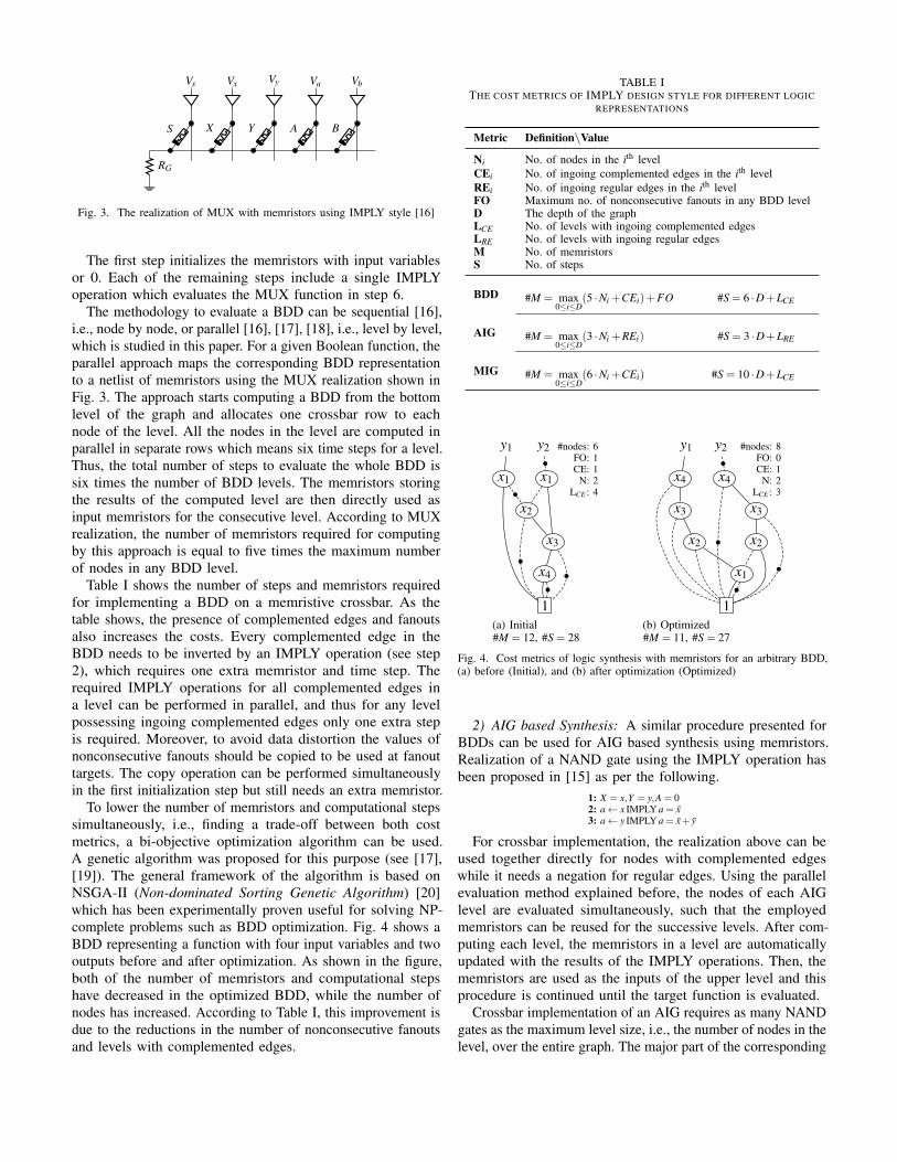
1) BDD based Synthesis: The starting point for BDD basedsynthesis is to realize the logic primitive designating eachgraph node, i.e., a 2-to-1 multiplexer (MUX), with memristors.Fig. 3 shows the MUX realization proposed for this purposein [16]. This realization executes the MUX function within sixsteps performed in five memristors. Memristors S, X , and Ystore the inputs and the two others, A and B, are required forthe IMPLY operations. The corresponding computational stepsare as follows:
1: S = s,X = x,Y = y,A = 0,B = 02: a← s IMPLY a = s3: a← y IMPLY a = y+ s4: b← a IMPLY b = y · s5: s← x IMPLY s = x+ s6: b← s IMPLY b = x · s+ y · s
RG
S X Y A B
Vs Vx Vy Va Vb
Fig. 3. The realization of MUX with memristors using IMPLY style [16]
The first step initializes the memristors with input variablesor 0. Each of the remaining steps include a single IMPLYoperation which evaluates the MUX function in step 6.
The methodology to evaluate a BDD can be sequential [16],i.e., node by node, or parallel [16], [17], [18], i.e., level by level,which is studied in this paper. For a given Boolean function, theparallel approach maps the corresponding BDD representationto a netlist of memristors using the MUX realization shown inFig. 3. The approach starts computing a BDD from the bottomlevel of the graph and allocates one crossbar row to eachnode of the level. All the nodes in the level are computed inparallel in separate rows which means six time steps for a level.Thus, the total number of steps to evaluate the whole BDD issix times the number of BDD levels. The memristors storingthe results of the computed level are then directly used asinput memristors for the consecutive level. According to MUXrealization, the number of memristors required for computingby this approach is equal to five times the maximum numberof nodes in any BDD level.
Table I shows the number of steps and memristors requiredfor implementing a BDD on a memristive crossbar. As thetable shows, the presence of complemented edges and fanoutsalso increases the costs. Every complemented edge in theBDD needs to be inverted by an IMPLY operation (see step2), which requires one extra memristor and time step. Therequired IMPLY operations for all complemented edges ina level can be performed in parallel, and thus for any levelpossessing ingoing complemented edges only one extra stepis required. Moreover, to avoid data distortion the values ofnonconsecutive fanouts should be copied to be used at fanouttargets. The copy operation can be performed simultaneouslyin the first initialization step but still needs an extra memristor.
To lower the number of memristors and computational stepssimultaneously, i.e., finding a trade-off between both costmetrics, a bi-objective optimization algorithm can be used.A genetic algorithm was proposed for this purpose (see [17],[19]). The general framework of the algorithm is based onNSGA-II (Non-dominated Sorting Genetic Algorithm) [20]which has been experimentally proven useful for solving NP-complete problems such as BDD optimization. Fig. 4 shows aBDD representing a function with four input variables and twooutputs before and after optimization. As shown in the figure,both of the number of memristors and computational stepshave decreased in the optimized BDD, while the number ofnodes has increased. According to Table I, this improvement isdue to the reductions in the number of nonconsecutive fanoutsand levels with complemented edges.
TABLE ITHE COST METRICS OF IMPLY DESIGN STYLE FOR DIFFERENT LOGIC
REPRESENTATIONS
Metric Definition\Value
Ni No. of nodes in the ith levelCEi No. of ingoing complemented edges in the ith levelREi No. of ingoing regular edges in the ith levelFO Maximum no. of nonconsecutive fanouts in any BDD levelD The depth of the graphLCE No. of levels with ingoing complemented edgesLRE No. of levels with ingoing regular edgesM No. of memristorsS No. of steps
BDD #M = max0≤i≤D
(5 ·Ni +CEi)+FO #S = 6 ·D+LCE
AIG #M = max0≤i≤D
(3 ·Ni +REi) #S = 3 ·D+LRE
MIG #M = max0≤i≤D
(6 ·Ni +CEi) #S = 10 ·D+LCE
y1 y2
x2
x4
x1 x1
x3
1
#nodes: 6FO: 1CE: 1
N: 2LCE : 4
(a) Initial#M = 12, #S = 28
y1 y2
x3
x2
x1
x4
x3
x2
x4
1
#nodes: 8FO: 0CE: 1
N: 2LCE : 3
(b) Optimized#M = 11, #S = 27
Fig. 4. Cost metrics of logic synthesis with memristors for an arbitrary BDD,(a) before (Initial), and (b) after optimization (Optimized)
2) AIG based Synthesis: A similar procedure presented forBDDs can be used for AIG based synthesis using memristors.Realization of a NAND gate using the IMPLY operation hasbeen proposed in [15] as per the following.
1: X = x,Y = y,A = 02: a← x IMPLY a = x3: a← y IMPLY a = x+ y
For crossbar implementation, the realization above can beused together directly for nodes with complemented edgeswhile it needs a negation for regular edges. Using the parallelevaluation method explained before, the nodes of each AIGlevel are evaluated simultaneously, such that the employedmemristors can be reused for the successive levels. After com-puting each level, the memristors in a level are automaticallyupdated with the results of the IMPLY operations. Then, thememristors are used as the inputs of the upper level and thisprocedure is continued until the target function is evaluated.
Crossbar implementation of an AIG requires as many NANDgates as the maximum level size, i.e., the number of nodes in thelevel, over the entire graph. The major part of the corresponding

Sense amplifiers
Column decoders and voltage drivers
Row
deco
ders
and
volta
gedr
iver
s
. . .
. . .
. . .
...
...
...
...
. . .
R11 R12 R13 R1m
R21 R22 R23 R2m
Rn1 Rn2 Rn3 Rnm
(a)
3
1 2level 1
level 2
f = x⊕ y⊕ z
x
x y z y x(b)
#R = 6
(c)
Fig. 5. Standard memristive crossbar for the presented synthesis approach.(a) MIG representing a three bit XOR gate, and (b) upper-bound crossbar forits crossbar implementation.
number of memristors and time steps for implementation isthree times the number of required NAND gates and threetimes the number of AIG levels, respectively (see Table I). Thevalues in the table also include additional memristors neededfor the required NOT operations, i.e., the regular edges in therealization.
The costs shown in Table I can be reduced with respect tothe number of time steps or devices, addressing the latencyand area of the resulting implementations. ABC [21] providescommands for rewriting AIGs to more efficient ones. To lowerthe number of required memristors, the command dc2 can beused to lower the number of nodes in the graph.
Latency of the designs can also be reduced before mappingthem to their corresponding netlist of memristors by the ABCcommand if -x -g. The command minimizes the depth of theAIG which is indeed the most significant term in the numberof time steps because of being multiplied by a factor of three.Applying any of these commands iteratively can considerablyreduce the targeted cost metric.
3) MIG based Synthesis: The realization for the majoritygate using the IMPLY operation was proposed in [22] and isas the following:
01: X = x,Y = y,Z = zA = 0,B = 0,C = 0
06: c← y IMPLY c = x+ y
02: a← x IMPLY a = x 07: c← z IMPLY c = x · z+ y · z03: b← y IMPLY b = y 08: a = 004: y← a IMPLY y = x+ y 09: a← b IMPLY a = x · y05: b← x IMPLY b = x+ y 10: a← c IMPLY a = x · y+ y · z+ x · z.
The realization needs ten IMPLY steps and six memristors.However, it is worth mentioning that a majority based designstyle beyond the scope of this paper was proposed in [23] andwas shown more efficient when using MIGs [22].
The cost metrics for the parallel evaluation of MIG basedapproach using IMPLY are given in Table I. The values in thetable are obtained similarly to the explanation given for BDDsand AIGs but according to the realization of majority gate. Thecomplete set of logic axioms to optimize an arbitrary MIG toa logically equivalent MIG with smaller number of nodes orlevels was proposed in [24]. In [18], several MIG optimizationalgorithms have been proposed which can be employed tolower the cost metrics of crossbar implementation with respectto both area and latency.
Fig. 5(a) shows a standard multi-row/column memristivecrossbar required for presented synthesis approach. For thesake of clarity, we present step-by-step implementation of anexample MIG shown in Fig. 5(b). The MIG has a maximumlevel size of 2 which needs an upper bound of 12 (2×6)memristors placed in two rows besides one more for the ingoingcomplemented edges (see Fig. 5(c)). As Table I suggests, thecomputation needs 22 steps, 2×10 for the two levels and twomore steps for the complemented edges. The implementationsteps are listed below:
Initialization: Ri j = 0;
1: Loading variables for level 1: R11 = x,R12 = y,R13 = z;R21 = x,R22 = y,R23 = z;
2: Negation for node 1: R17← x IMPLY R17 : R17 = x;
3-11: Computing level 1: node 1: R14 = M(x,y,z);node 2: R24 : M(x,y,z);
12: Loading variables for level 2: R11 = x,R12 = M(x,y,z),R13 = M(x,y,z)R14 = R15 = R16 = R17 = 0;
13: Negation for node 3: R17← R12 IMPLY R17 :R17 = R12 = M(x,y,z);
14-22: Computing level 2 (root node): R14 = M(M(x,y,z),x,M(x,y,z));
The names Ri1 to Ri6 in the implementation steps aboverespectively designate the resistance states of the memristorsshown by X ,Y,Z,A,B, and C used for the realization of themajority gate. For initialization, all of the memristors in theentire crossbar are cleared. Since IMPLY needs all the variablesto be stored in the same horizontal line, there may be a needto have several copies of primary inputs or intermediate resultsat different rows. This is shown in step 1, where each variableof nodes 1 and 2 are loaded into two memristors in both rows.Step 2 computes the complemented edge, i.e., showed by adot, of node 1 in the seventh memristor considered for thiscase at the end of first row, R17. Steps 3-11 compute bothnodes at level one which updates R14 and R24 by the resultsof the computations. Step 12 loads the inputs of level 2 whichincludes a single node, i.e., the root node. The complementededge originating at node 2 is negated in step 13, and then theroot node is computed in step 22.
B. MAGIC Design Style
MAGIC is the acronym for memristor aided logic [7], whichis a stateful logic design style where the resitance valuesrepresent the logic states. The input(s) and output values arestored in different memristors. All basic gates (NOT, AND,

OR, NOR, NAND) can be implemented using the MAGICdesign style, as illustrated in Fig. 6.
Fig. 6. Basic gates realized using the MAGIC design style.
A MAGIC gate operation requires two sequential steps:i) In the first step the output memristor is initialized to a
known value (either 0 or 1). For non-inverting gates likeAND/OR it is initialized to 0, while for inverting gateslike NOT/NOR/NAND it is initialized to 1.
ii) In the second step a suitable voltage V0 is applied tothe input memristor(s). The voltage across the outputmemristor depends upon the logical state of the inputand output memristor, and switches accordingly.
Fig. 7. 2-input MAGIC NOR gate and equivalent circuit mapped in crossbar
Though all gates can be implemented using the MAGICdesign style; however, only NOR and NOT gate can be mappedto memristor crossbars. A crossbar consists of horizontal andvertical nanowires, where the memristors are fabricated at thejunctions. Fig. 7 shows the crossbar mapping of a 2-input NORgate. For synthesizing larger boolean functions, the functionsare first represented in terms of NOR and NOT gates, and thenvarious mapping techniques [25], [26] are used to map thegates to the crossbar.
IV. NEAR MEMORY AND IN-MEMORY COMPUTING:CHALLENGES AND IMPLEMENTATION ISSUES
A. In-Memory Computing
As explained in Section III, both of the two discussedstyles for logic-in-memory computing result in sequences ofcomputational steps. Accordingly, lowering the number of steps
as well as the number of memristors are considered importantobjectives for in-memory computing architectures [27]. For thispurpose, usually memristors storing the intermediate results arereused for computation in the successive steps to avoid usageof extra steps or devices [28]. The successive switching ofsome memristors compared to the other devices in a memristivecrossbar results in an unbalanced write traffic. Considering thefact that the resistive switching devices have basically lowwrite endurance, i.e., in the best cases about 1010 [29] to 1011
write counts [30], this problem can lower the reliable lifetimeof the entire crossbar architecture.
Using IMPLY for synthesis, unbalanced distribution of writeshappens due to the lack of commutativity property, whichresults in higher write traffic in the memory cell storing theoutput of the operation. For example in [15], an implementationfor the NAND gate requiring two memristors and three timesteps was proposed. The implementation needs to switch onememristor, the so-called work device, at each of the threesteps while the other memristor is switched only once forinitialization which is called input memristor. Similarly, in[31], a synthesis approach has been proposed which considersonly two work memristors besides N input devices, where Nis the number of input variables of the Boolean function. Inthis case, the work devices wear out fast and therefore lowerthe lifetime of the design. In such implementations, the writetraffic can be distributed more evenly only by allocating extradevices to replace those with high write counts. This also costsadditional steps to copy the contents of memristors which isoften avoided for the sake of efficiency.
B. Near-Memory Computing
In [26] Thangkhiew et al. presented a near-memory map-ping scheme, where various adder circuits were mapped tomemristive crossbar array using the MAGIC design style. Theterm near-memory signifies that the input memristors need tobe configured prior to the evaluation as opposed to in-memorycomputing, where the inputs are already present in memory.Broadly two mapping techniques are discussed, serial andparallel. In serial mapping the gates are evaluated one by one,and in parallel mapping, several gates are evaluated in a singletime step. For carrying out the operations, several voltages [25]need to be applied to the rows/columns of the crossbar as:
a) A voltage Vset applied in column i and GND to row jinitializes the memristor at (i, j) to 1.
b) A voltage Vclear applied in column i and GND to row jinitializes the memristor at (i, j) to 0.
c) A voltage Vo applied to the columns corresponding toinputs of a gate, and GND to the column correspondingto the output, performs the NOR gate operation.
d) During a NOR gate operation, a voltage Viso applied toa row i disables the gate operation in row i.
To reduce the hardware cost, a level-wise mapping approachis presented in which the gates are mapped level by level. Toillustrate the parallel and level-wise mapping let us considerthe circuit shown in Fig. 8(a).
The snapshot for the evaluation of gates in level 1 is shownin Fig. 8(b). It can be observed that in level 1 the inputs (A,C
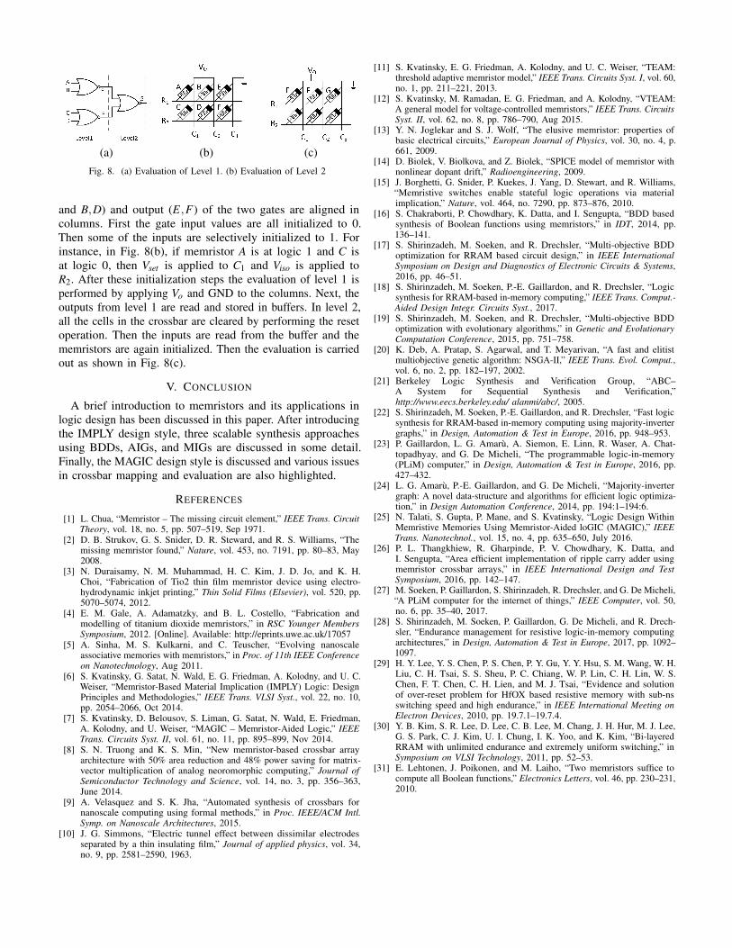
(a) (b) (c)Fig. 8. (a) Evaluation of Level 1. (b) Evaluation of Level 2
and B,D) and output (E,F) of the two gates are aligned incolumns. First the gate input values are all initialized to 0.Then some of the inputs are selectively initialized to 1. Forinstance, in Fig. 8(b), if memristor A is at logic 1 and C isat logic 0, then Vset is applied to C1 and Viso is applied toR2. After these initialization steps the evaluation of level 1 isperformed by applying Vo and GND to the columns. Next, theoutputs from level 1 are read and stored in buffers. In level 2,all the cells in the crossbar are cleared by performing the resetoperation. Then the inputs are read from the buffer and thememristors are again initialized. Then the evaluation is carriedout as shown in Fig. 8(c).
V. CONCLUSION
A brief introduction to memristors and its applications inlogic design has been discussed in this paper. After introducingthe IMPLY design style, three scalable synthesis approachesusing BDDs, AIGs, and MIGs are discussed in some detail.Finally, the MAGIC design style is discussed and various issuesin crossbar mapping and evaluation are also highlighted.
REFERENCES
[1] L. Chua, “Memristor – The missing circuit element,” IEEE Trans. CircuitTheory, vol. 18, no. 5, pp. 507–519, Sep 1971.
[2] D. B. Strukov, G. S. Snider, D. R. Steward, and R. S. Williams, “Themissing memristor found,” Nature, vol. 453, no. 7191, pp. 80–83, May2008.
[3] N. Duraisamy, N. M. Muhammad, H. C. Kim, J. D. Jo, and K. H.Choi, “Fabrication of Tio2 thin film memristor device using electro-hydrodynamic inkjet printing,” Thin Solid Films (Elsevier), vol. 520, pp.5070–5074, 2012.
[4] E. M. Gale, A. Adamatzky, and B. L. Costello, “Fabrication andmodelling of titanium dioxide memristors,” in RSC Younger MembersSymposium, 2012. [Online]. Available: http://eprints.uwe.ac.uk/17057
[5] A. Sinha, M. S. Kulkarni, and C. Teuscher, “Evolving nanoscaleassociative memories with memristors,” in Proc. of 11th IEEE Conferenceon Nanotechnology, Aug 2011.
[6] S. Kvatinsky, G. Satat, N. Wald, E. G. Friedman, A. Kolodny, and U. C.Weiser, “Memristor-Based Material Implication (IMPLY) Logic: DesignPrinciples and Methodologies,” IEEE Trans. VLSI Syst., vol. 22, no. 10,pp. 2054–2066, Oct 2014.
[7] S. Kvatinsky, D. Belousov, S. Liman, G. Satat, N. Wald, E. Friedman,A. Kolodny, and U. Weiser, “MAGIC – Memristor-Aided Logic,” IEEETrans. Circuits Syst. II, vol. 61, no. 11, pp. 895–899, Nov 2014.
[8] S. N. Truong and K. S. Min, “New memristor-based crossbar arrayarchitecture with 50% area reduction and 48% power saving for matrix-vector multiplication of analog neoromorphic computing,” Journal ofSemiconductor Technology and Science, vol. 14, no. 3, pp. 356–363,June 2014.
[9] A. Velasquez and S. K. Jha, “Automated synthesis of crossbars fornanoscale computing using formal methods,” in Proc. IEEE/ACM Intl.Symp. on Nanoscale Architectures, 2015.
[10] J. G. Simmons, “Electric tunnel effect between dissimilar electrodesseparated by a thin insulating film,” Journal of applied physics, vol. 34,no. 9, pp. 2581–2590, 1963.
[11] S. Kvatinsky, E. G. Friedman, A. Kolodny, and U. C. Weiser, “TEAM:threshold adaptive memristor model,” IEEE Trans. Circuits Syst. I, vol. 60,no. 1, pp. 211–221, 2013.
[12] S. Kvatinsky, M. Ramadan, E. G. Friedman, and A. Kolodny, “VTEAM:A general model for voltage-controlled memristors,” IEEE Trans. CircuitsSyst. II, vol. 62, no. 8, pp. 786–790, Aug 2015.
[13] Y. N. Joglekar and S. J. Wolf, “The elusive memristor: properties ofbasic electrical circuits,” European Journal of Physics, vol. 30, no. 4, p.661, 2009.
[14] D. Biolek, V. Biolkova, and Z. Biolek, “SPICE model of memristor withnonlinear dopant drift,” Radioengineering, 2009.
[15] J. Borghetti, G. Snider, P. Kuekes, J. Yang, D. Stewart, and R. Williams,“Memristive switches enable stateful logic operations via materialimplication,” Nature, vol. 464, no. 7290, pp. 873–876, 2010.
[16] S. Chakraborti, P. Chowdhary, K. Datta, and I. Sengupta, “BDD basedsynthesis of Boolean functions using memristors,” in IDT, 2014, pp.136–141.
[17] S. Shirinzadeh, M. Soeken, and R. Drechsler, “Multi-objective BDDoptimization for RRAM based circuit design,” in IEEE InternationalSymposium on Design and Diagnostics of Electronic Circuits & Systems,2016, pp. 46–51.
[18] S. Shirinzadeh, M. Soeken, P.-E. Gaillardon, and R. Drechsler, “Logicsynthesis for RRAM-based in-memory computing,” IEEE Trans. Comput.-Aided Design Integr. Circuits Syst., 2017.
[19] S. Shirinzadeh, M. Soeken, and R. Drechsler, “Multi-objective BDDoptimization with evolutionary algorithms,” in Genetic and EvolutionaryComputation Conference, 2015, pp. 751–758.
[20] K. Deb, A. Pratap, S. Agarwal, and T. Meyarivan, “A fast and elitistmultiobjective genetic algorithm: NSGA-II,” IEEE Trans. Evol. Comput.,vol. 6, no. 2, pp. 182–197, 2002.
[21] Berkeley Logic Synthesis and Verification Group, “ABC–A System for Sequential Synthesis and Verification,”http://www.eecs.berkeley.edu/ alanmi/abc/, 2005.
[22] S. Shirinzadeh, M. Soeken, P.-E. Gaillardon, and R. Drechsler, “Fast logicsynthesis for RRAM-based in-memory computing using majority-invertergraphs,” in Design, Automation & Test in Europe, 2016, pp. 948–953.
[23] P. Gaillardon, L. G. Amaru, A. Siemon, E. Linn, R. Waser, A. Chat-topadhyay, and G. De Micheli, “The programmable logic-in-memory(PLiM) computer,” in Design, Automation & Test in Europe, 2016, pp.427–432.
[24] L. G. Amaru, P.-E. Gaillardon, and G. De Micheli, “Majority-invertergraph: A novel data-structure and algorithms for efficient logic optimiza-tion,” in Design Automation Conference, 2014, pp. 194:1–194:6.
[25] N. Talati, S. Gupta, P. Mane, and S. Kvatinsky, “Logic Design WithinMemristive Memories Using Memristor-Aided loGIC (MAGIC),” IEEETrans. Nanotechnol., vol. 15, no. 4, pp. 635–650, July 2016.
[26] P. L. Thangkhiew, R. Gharpinde, P. V. Chowdhary, K. Datta, andI. Sengupta, “Area efficient implementation of ripple carry adder usingmemristor crossbar arrays,” in IEEE International Design and TestSymposium, 2016, pp. 142–147.
[27] M. Soeken, P. Gaillardon, S. Shirinzadeh, R. Drechsler, and G. De Micheli,“A PLiM computer for the internet of things,” IEEE Computer, vol. 50,no. 6, pp. 35–40, 2017.
[28] S. Shirinzadeh, M. Soeken, P. Gaillardon, G. De Micheli, and R. Drech-sler, “Endurance management for resistive logic-in-memory computingarchitectures,” in Design, Automation & Test in Europe, 2017, pp. 1092–1097.
[29] H. Y. Lee, Y. S. Chen, P. S. Chen, P. Y. Gu, Y. Y. Hsu, S. M. Wang, W. H.Liu, C. H. Tsai, S. S. Sheu, P. C. Chiang, W. P. Lin, C. H. Lin, W. S.Chen, F. T. Chen, C. H. Lien, and M. J. Tsai, “Evidence and solutionof over-reset problem for HfOX based resistive memory with sub-nsswitching speed and high endurance,” in IEEE International Meeting onElectron Devices, 2010, pp. 19.7.1–19.7.4.
[30] Y. B. Kim, S. R. Lee, D. Lee, C. B. Lee, M. Chang, J. H. Hur, M. J. Lee,G. S. Park, C. J. Kim, U. I. Chung, I. K. Yoo, and K. Kim, “Bi-layeredRRAM with unlimited endurance and extremely uniform switching,” inSymposium on VLSI Technology, 2011, pp. 52–53.
[31] E. Lehtonen, J. Poikonen, and M. Laiho, “Two memristors suffice tocompute all Boolean functions,” Electronics Letters, vol. 46, pp. 230–231,2010.