logic devices for interfacing, the 8085 mpu lecture...
TRANSCRIPT

Logic Devices for
Interfacing, The 8085
MPU
Lecture 4
1

Logic Devices for Interfacing
Tri-State devices
Buffer
Bidirectional Buffer
Decoder
Encoder
D Flip Flop :Latch and Clocked
2

Tri-state Logic Outputs
Since we can have multiple masters on a bus, we need Tri-state logic for attachment to a bus so that each device can choose to drive or not drive the bus depending on whether it is the bus master for a given bus cycle
Tri-state logic prevents a bus conflict where one device is driving a signal to 1 and another device is driving it to 0 at the same time - generates high current through wires (and smoke?)
3

Tri-State Logic and Buses The logical element has output enable pin to go from a
floating output to drive the output from the circuit
Inverters and buffers are used as bus drivers or buffers
Two such drivers or buffers in opposite directions are used to make the connection bi-directional
The gates also provide more “drive” onto the bus so that the bus signals are stronger and the bus can be longer
4
enableout
enablein
Device Bus
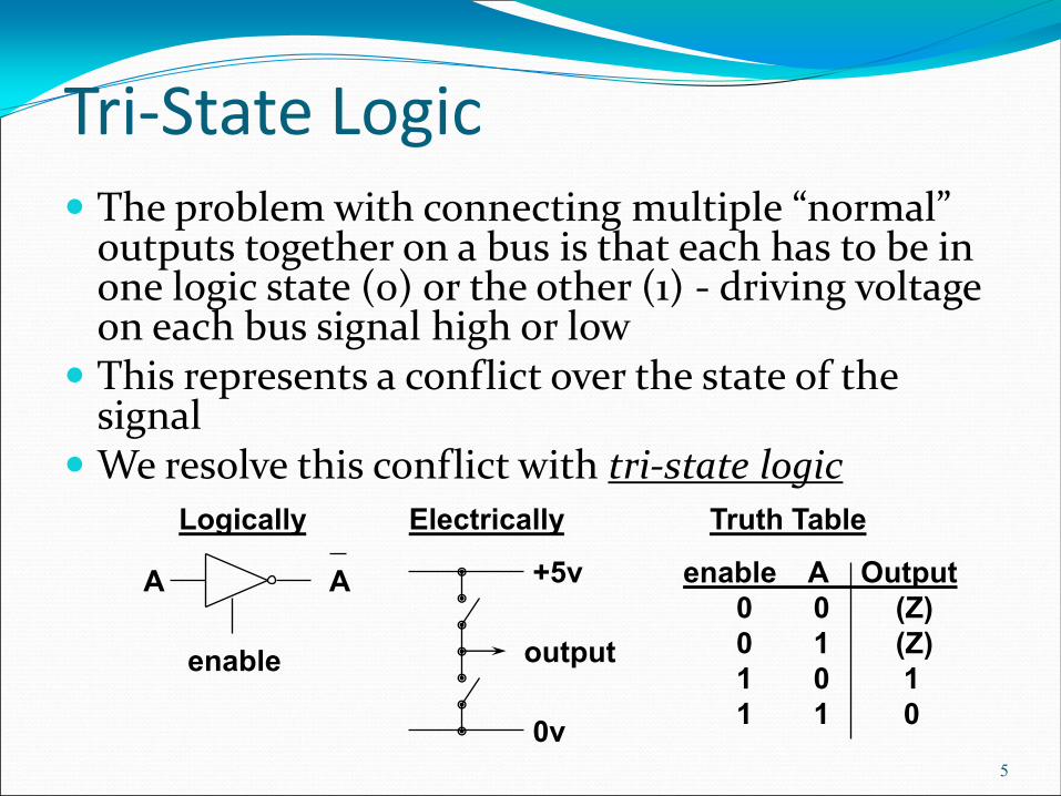
Tri-State Logic The problem with connecting multiple “normal”
outputs together on a bus is that each has to be in one logic state (0) or the other (1) - driving voltage on each bus signal high or low
This represents a conflict over the state of the signal
We resolve this conflict with tri-state logic
5
+5v
0v
output
Logically
A A
enable
Electrically Truth Table
enable A Output
0 0 (Z)
0 1 (Z)
1 0 1
1 1 0

Buses Concept is to link together multiple functional units
over a common data highway at a lower cost than using multiple point to point links
6
A
B
D
E
C
Bus
A
B
D
E
C
OR
Number of Links = n * (n – 1) / 2

Bus - Essential Part of Any Computer
7
CPU Primary
Memory
Secondary
Memory I/O
Data
Address
Control

Tri-State Logic and Buses
8

Bus Master – Slave Relationships Up till now, I have said that the address bus and the
control bus are always driven by the processor, however that is NOT really true!
That was only a “lie of simplification”!
The processor is NOT the only device that may be driving the address and control busses
Hopefully you are now well-prepared for me to un-simplify a bit
9

Bus Arbitration Bus arbitration is used to hand off a bus between one
of several potential bus masters using signals that are a part of the bus itself
A bus arbitration protocol implements some form of bus request and bus grant handshake to determine which device will be the master on the bus for the next bus cycle
10

Tri-State Bus Summary All devices have tri-state logic connections to the data
bus – may be driving or receiving
Memory and I/O devices don’t need tri-state logic on address/control bus (never drive them)
Because the processor may need to yield the control/address busses, it must have tri-state logic for driving those bus signals
DMAC controller must have tri-state logic for driving the control and address bus signals
11

BUFFER A buffer has only a single input and a single output
with behavior that is the opposite of an NOT gate. It simply passes its input, unchanged, to its output. In a Boolean logic simulator, a buffer is mainly used to increase propagation delay. In a real-world circuit, a buffer can be used to amplify a signal if its current is too weak.
12

DECODER A decoder is a device which does the reverse
operation of an encoder, undoing the encoding so that the original information can be retrieved. The same method used to encode is usually just reversed in order to decode. It is a combinational circuit that converts binary information from n input lines to a maximum of 2n unique output lines.
13

ENCODER An encoder is a device, circuit, transducer, software
program, algorithm or person that converts information from one format or code to another, for the purposes of standardization, speed, secrecy, security or compressions.
14

D FLIP FLOP: Latched and Clocked A flip-flop or latch is a circuit that has two stable states and can be
used to store state information. A flip-flop is a bistable multivibrator. The circuit can be made to change state by signals applied to one or more control inputs and will have one or two outputs.
The D flip-flop is widely used. It is also known as a "data" or "delay" flip-flop.
The D flip-flop captures the value of the D-input at a definite portion of the clock cycle (such as the rising edge of the clock). That captured value becomes the Q output. At other times, the output Q does not change. The D flip-flop can be viewed as a memory cell, a zero-order hold, or a delay line.
15

8085 MPU
16

1717
Intel 8085 Pin Intel 8085 Pin ConfigurationConfiguration

1818
Signals and I/O Pins

1919
Intel 8085 CPU Block DiagramIntel 8085 CPU Block Diagram

The 8085 and Its Buses The 8085 is an 8-bit general purpose microprocessor that can address
64K Byte of memory.
It has 40 pins and uses +5V for power. It can run at a maximum frequency of 3 MHz.
The pins on the chip can be grouped into 6 groups:
Address Bus.
Data Bus.
Control and Status Signals.
Power supply and frequency.
Externally Initiated Signals.
Serial I/O ports.

The Address and Data Bus Systems
The address bus has 8 signal lines A8 – A15 which are unidirectional.
The other 8 address bits are multiplexed (time shared) with the 8 data bits.
So, the bits AD0 – AD7 are bi-directional and serve as A0 – A7 and D0 – D7 at the same time.
During the execution of the instruction, these lines carry the address bits during the early part, then during the late parts of the execution, they carry the 8 data bits.
In order to separate the address from the data, we can use a latch to save the value before the function of the bits changes.

The Control and Status Signals There are 4 main control and status signals. These are:
ALE: Address Latch Enable. This signal is a pulse that become 1 when the AD0 – AD7 lines have an address on them. It becomes 0 after that. This signal can be used to enable a latch to save the address bits from the AD lines.
RD: Read. Active low.
WR: Write. Active low.
IO/M: This signal specifies whether the operation is a memory operation (IO/M=0) or an I/O operation (IO/M=1).
S1 and S0 : Status signals to specify the kind of operation being performed. Usually not used in small systems.

The Flags register There is also a flag register whose bits are affected by the arithmetic & logic
operations.
S-sign flag
The sign flag is set if bit D7 of the accumulator is set after an arithmetic or logic operation.
Z-zero flag
Set if the result of the ALU operation is 0. Otherwise is reset. This flag is affected by operations on the accumulator as well as other registers. (DCR B).
AC-Auxiliary Carry
This flag is set when a carry is generated from bit D3 and passed to D4 . This flag is used only internally for BCD operations.
P-Parity flag
After an ALU operation, if the result has an even # of 1s, the p-flag is set. Otherwise it is cleared. So, the flag can be used to indicate even parity.
CY-carry flag
This flag is set when a carry is generated from bit D7 after an unsigned operation.
OV-Overflow flag
This flag is set when an overflow occurs after a signed operation.

More on the 8085 machine cycles The 8085 executes several types of instructions with
each requiring a different number of operations of different types. However, the operations can be grouped into a small set.
The three main types are: Memory Read and Write.
I/O Read and Write.
Request Acknowledge.
These can be further divided into various smaller operations (machine cycles).
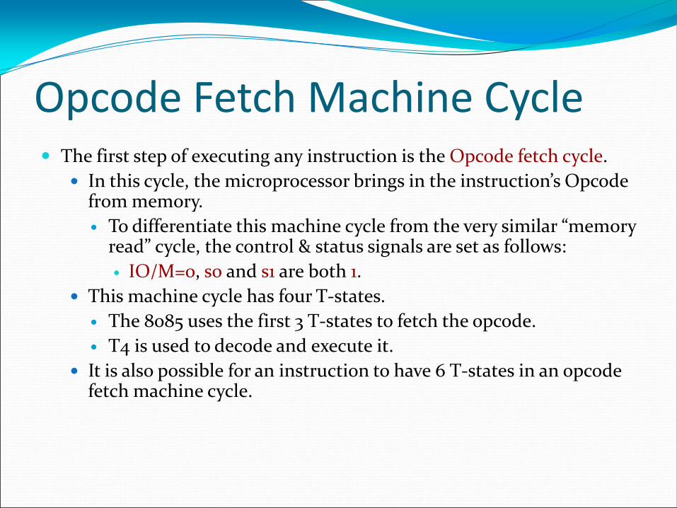
Opcode Fetch Machine Cycle The first step of executing any instruction is the Opcode fetch cycle.
In this cycle, the microprocessor brings in the instruction’s Opcode from memory.
To differentiate this machine cycle from the very similar “memory read” cycle, the control & status signals are set as follows:
IO/M=0, s0 and s1 are both 1.
This machine cycle has four T-states.
The 8085 uses the first 3 T-states to fetch the opcode.
T4 is used to decode and execute it.
It is also possible for an instruction to have 6 T-states in an opcode fetch machine cycle.

Memory Read Machine Cycle The memory read machine cycle is exactly the same as
the opcode fetch except:
It only has 3 T-states
The s0 signal is set to 0 instead.

The Memory Read Machine Cycle
To understand the memory read machine cycle, let’s study the execution of the following instruction:
MVI A, 32
In memory, this instruction looks like:
The first byte 3EH represents the opcode for loading a byte into the accumulator (MVI A), the second byte is the data to be loaded.
The 8085 needs to read these two bytes from memory before it can execute the instruction. Therefore, it will need at least two machine cycles.
The first machine cycle is the opcode fetch discussed earlier.
The second machine cycle is the Memory Read Cycle.
2000H
2001H
3E
32