low power and area delay efficient carry select adder
DESCRIPTION
M.Tech-ECE ProjectTRANSCRIPT

Area–Delay–Power Efficient Carry-Select Adder
Area–Delay–Power Efficient Carry-Select
Adder
ABSTRACT: Design of area and power-efficient high speed data path logic systems are one of
the most substantial areas of research in VLSI system design. In digital adders, the speed of
addition is limited by the time required to propagate a carry through the adder. The sum for each
bit position in an elementary adder is generated sequentially only after the previous bit position
has been summed and a carry propagated into the next position. The CSLA is used in many
computational systems to alleviate the problem of carry propagation delay by independently
generating multiple carries and then select a carry to generate the sum Carry Select Adder
(CSLA) is one of the fastest adders used in many data-processing processors to perform fast
Page 1
Area–Delay–Power Efficient Carry-Select Adder
arithmetic functions. From the structure of the CSLA, it is clear that there is scope for reducing
the area and power consumption in the CSLA. This work uses a simple and efficient gate-level
modification to significantly reduce the area and power of the CSLA. Based on this modification
8-, 16-, 32-, and 64-b square-root CSLA (SQRT CSLA) architecture have been developed and
compared with the regular SQRT CSLA architecture. The proposed design has reduced area and
power as compared with the regular SQRT CSLA with only a slight increase in the delay. This
work evaluates the performance of the proposed designs in terms of delay, area, power, and their
products by hand with logical effort and through custom design and layout in 0.18-m CMOS
process technology. The results analysis shows that the proposed CSLA structure is better than
the regular SQRT CSLA.
Keywords—Application-specific integrated circuit (ASIC), area efficient, CSLA, low power.
LIST OF CONTENTS Page No
ABSTRACT i
LIST OF FIGURES ii
LIST OF TABLES iv
LIST OF SYMBOLS v
NOMENCLATURE viCHAPTER 1 INTRODUCTION 1-5
1.1 Droop Based Control 2
Page 2

Area–Delay–Power Efficient Carry-Select Adder
1.2 Hybrid Control 3
1.2.1 Difficulties with hybrid voltage control method 3
1.3 Unified control strategy 4
1.4 Organization of the thesis 5
CHAPTER 2 LITERATURE REVIEW 6-35
2.1 Distributed generation 7
2.2 Various types of DG generators 8
2.3 Advantages of DG 9
2.4 Disadvantages of DG 9
2.5 Introduction to DG & intentional islanding 9
2.5.1 DG& intentional islanding 9
2.6 Types and commonalities of DG & PCS systems 10
2.7 Basics for the design of a DG power conversion system 14
2.7.1 Focus on VSI of the PCS 14
2.7.2 Standards and common practices for grid interconnections 15
2.7.3 Challenges for medium & high power inverters 16
2.8 Islanded and interconnected DG 18
2.8.1 Generators, IOU, PU 19
2.8.2 Transmission grids, basis points, ISO 19
2.8.3 Distribution grid 19
2.9 Introduction to multi level inverters 21
2.9.1 H – bridge inverter 22
2.9.2 Cascaded H-bridge multilevel inverter 24
2.9.3 Multilevel inverter structures 25
2.9.4 Types of multilevel inverters 27
Page 3

Area–Delay–Power Efficient Carry-Select Adder
2.9.5 Multilevel power converter structures 28
2.9.6 Advantages of multilevel inverter 29
2.10 Space vector pulse width modulation 29
2.10.1 Space vector concept 30
2.10.2 Switching states 32
2.10.3 Space vector modulation 33
2.10.4 Implementing SVPWM 34
2.10.5 Sector selection based SVPWM 35
CHAPTER 3 PROPOSEDCONTROLSTRATEGY 36-49
3.1 Proposed control strategy 37
3.1.1 Power stage 37
3.1.2 Basic idea 37
3.2 Control scheme 39
3.3 Operation principle of DG 42
3.3.1 Grid-tied mode 42
3.3.2 Transition from the grid-tied mode to the islanded mode 45
3.3.3 Islanded mode 48
3.3.4 Transition from the islanded mode to the grid-tied mode 49
CHAPTER 4 ANALYSIS AND DESIGN 50-58
4.1 Steady state 51
4.2 Transient state 54
CHAPTER-5 MATLAB CIRCUITS & RESULTS 59-67
CONCLSION & FUTURE SCOPE 68
BIBILOGRAPHY 69
PUBLISHED PAPER
LIST OF FIGURES
Page 4
Area–Delay–Power Efficient Carry-Select Adder
S.No Figure Details Page No
Fig.2.1 Conventional electrical network 8
Fig.2.2 Distributed Generation (DG) Electricity 8
Fig.2.3 Islanding Diagram 10
Fig .2.4 (a) DC DER based PCS; (b) AC DER based PCS 11
Fig .2.5 (a) Top, Area EPSs of a Utility System showing DG interconnection 13
Fig. 2.5 (b)Black diagram of DER, PCS, Area EPS, and the grid interconnection 13
Fig.2.6 Distribution Grid Topology 20
Fig. 2.7 Half Bridge Inverter 23
Fig. 2.8 Full Bridge Inverter 23
Fig.2.9 Output waveform of Half Bridge Inverter 24
Fig.2.10 Output waveform of Full Bridge Inverter 24
Fig. 2.11 One phase leg of an inverter with different configurations 26
Fig.2.12 Relationship of abc reference frame and stationary dq reference frame 30
Fig.2.13 Basic switching, vectors and sectors 31
Fig.2.14 (a) Output voltage vector in the α-β plane 33
Fig. 2.14 (b) Output line voltages in time domain 33
Fig. 2.15 Synthesis of the required output voltage vector in sector 1 34
Fig. 3.1 Schematic diagram of the DG based on the proposed control strategy 38
Fig. 3.2 Overall block diagram of the proposed unified control strategy 38
Fig. 3.3 Block diagram of the current reference generation module 40
Fig. 3.4 Simplified block diagram of the unified control strategy when DG 44
Fig. 3.5 Operation sequence during the transition from the grid-tied mode to 46
the islanded mode
Fig. 3.6 Transient process of the voltage and current when the islanding happens 46
Fig. 3.7 Simplified block diagram of the unified control strategy when DG 48
Operates in the islanded mode
Fig. 4.1 Block diagram of the simplified voltage loop 56
Fig.5.1 Simulation diagram when DG is in the grid-tied mode 60
Fig: 5.2 Simulation waveforms when DG is in the grid-tied mode 61
Fig.5.3 Simulation diagram of DG is transferred from the grid-tied 62
Page 5

Area–Delay–Power Efficient Carry-Select Adder
Mode to the islanded mode
Fig.5.4 Simulation waveforms when DG is transferred from the grid-tied mode 62
To the islanded mode
Fig.5.5 Simulation diagram when DG is transferred from the islanded mode 63
To the grid-tied mode
Fig .5.6 Simulation waveforms when DG is transferred from the islanded mode 64
To the grid-tied mode
Fig .5.7 Simulation diagram when DG feeds nonlinear load in islanded mode 65
Fig .5.8 Experimental waveform when DG feeds nonlinear load in 65
Islanded mode with load current feedforward
Fig. 5.9 Simulation diagram when DG is transferred from the Islanded mode
To the grid-tied mode using multilevel inverter topology 66
Fig 5.10 Simulation waveforms under DG is transferred from the 66
Islanded mode to the grid-tied mode
Fig.5.11 Five Level Output Voltage of Proposed Three Phase Multilevel 67
Inverter Fed DG Scheme using Unified Control Scheme
LIST OF TABLES
Page 6

Area–Delay–Power Efficient Carry-Select Adder
S.No Table title Page No
Table1 Examples of specific DERs and the needed PCS functions for interconnections 13Table2 Switching pattern of 3 level full bridge inverter 23
Table3 Switching patterns and output vectors 32
Table4 Parameters of the power stage Multi Level Inverter 56
Table5 Parameters Used In Unified Control Strategy
Using Three Phase Inverter 66
CHAPTER 1
INTRODUCTION
INTRODUCTION
VLSI stands for Very large scale integration which refers to those integrated circuits thatcontain more than 107transistors. Designing such circuit is difficult and that design needs toovercome the VLSI design problem like Area, Speed, Power dissipation, Design time andTestability. In digital adders, the speed of addition is limited by the time required to propagate a
Page 7

Area–Delay–Power Efficient Carry-Select Adder
carry through the adder. The sum for each bit position in an elementary adder is generatedsequentially only after the previous bit position has been summed and a carry propagated into thenext position. The early years carry look a head adder used to overcome the delay it will produceall produce all the carries at time but it requires more circuitry, next those are replaced by carryselect adders using dual RCAs. In this sum is generated for Cin=1 and Cin=0, depends on inputcarry one sum is passed as final sum using multiplexer. The problem is again, it requires morecircuitry because it requires two full adders at each stage of three bits addition. That is replacedby one RCA and one add-one circuit. There again the same problem that is eliminated by thisproposed system CSLA using BEC. The basic idea of this work is to use Binary to Excess-1Converter (BEC) instead of RCA with Cin = 1 in the regular CSLA to achieve lower area andpower consumption.
The main advantage of this BEC logic comes from the lesser number of logic gates thanthe n-bit Full Adder (FA) structure. The carry-select adder generally consists of two ripple carryadders and a multiplexer. Adding two n-bit numbers with a carry-select adder is done with twoadders (therefore two ripple carry adders) in order to perform the calculation twice, one timewith the assumption of the carry being zero and the other assuming one. After the two results arecalculated, the correct sum, as well as the correct carry, is then selected with the multiplexer oncethe correct carry is known. The number of bits in each carry select block can be uniform, orvariable. In the uniform case, the optimal delay occurs for a block size of n variable, the blocksize should have a delay, from additional inputs A and B to the carry out, equal to that of themultiplexer chain leading into it, so that the carry out is calculated just in time. The delay isderived from uniform sizing, where the ideal number of full-adder elements per block is equal tothe square root of the number of bits being added, since that will yield an equal number of MUXdelays.
Two 4-bit ripple carry adders are multiplexed together, where the resulting carry and sumbits are selected by the carry-in. Since one ripple carry adder assumes a carry-in of 0, and theother assumes a carry-in of 1, selecting which adder had the correct assumption via the actualcarry-in yields the desired result. A 16-bit carry-select adder with a uniform block size of 4 can be created with three of these blocks and a 4-bit ripple carryadder. Since carry-in is known at the beginning of computation, a carry select block is not neededfor the first four bits. The delay of this adder will be four full adder delays, plus three MUXdelays A 32-bit carry-select adder with variable size can be similarly created. Here we show anadder with block sizes. This break-up is ideal when the full-adder delay is equal to the MUXdelay, which is unlikely. The total delay is two full adder delays, and four MUX delays. Additionis the heart of computer arithmetic, and the arithmetic unit is often the work horse of acomputational circuit. They are the necessary component of a data path, e.g. in microprocessorsor a signal processor. There are many ways to design an adder.
The Ripple Carry Adder (RCA) provides the most compact design but takes longercomputing time. If there is N-bit RCA, the delay is linearly proportional to N. Thus for largevalues of N the RCA gives highest delay of all adders. The Carry Look Ahead Adder (CLA)gives fast results but consumes large area. If there is N-bit adder, CLA is fast for N≤4, but forlarge values of N its delay increases more than other adders. So for higher number of bits, CLAgives higher delay than other adders due to presence of large number of fan-in and a largenumber of logic gates. The Carry Select Adder (CSA) provides a compromise between small areabut longer delay RCA and a large area with shorter delay CLA. In rapidly growing mobileindustry, faster units are not the only concern but also smaller area and less power become major
Page 8

Area–Delay–Power Efficient Carry-Select Adder
concerns for design of digital circuits. In mobile electronics, reducing area and powerconsumption are key factors in increasing portability and battery life. Even in servers anddesktop computers power dissipation is an important design constraint. Design of area- andpower-efficient high-speed data path logic systems are one of the most substantial areas ofresearch in VLSI system design. In digital adders, the speed of addition is limited by the timerequired to propagate a carry through the adder.
CHAPTER 3 BLOCK DIAGRAM 3.1 BLOCK DIAGRAM FOR REGULAR CSLA
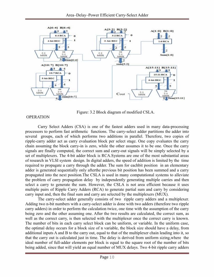
Figure: 3.1 Block diagram of regular CSLA 3.2 BLOCK DIAGRAM OF MODIFIED CSLA
Page 9
Area–Delay–Power Efficient Carry-Select Adder
Figure: 3.2 Block diagram of modified CSLA. OPERATION
Carry Select Adders (CSA) is one of the fastest adders used in many data-processingprocessors to perform fast arithmetic functions. The carry-select adder partitions the adder intoseveral groups, each of which performs two additions in parallel. Therefore, two copies ofripple-carry adder act as carry evaluation block per select stage. One copy evaluates the carrychain assuming the block carry-in is zero, while the other assumes it to be one. Once the carrysignals are finally computed, the correct sum and carry-out signals will be simply selected by aset of multiplexers. The 4-bit adder block is RCA.Systems are one of the most substantial areasof research in VLSI system design. In digital adders, the speed of addition is limited by the timerequired to propagate a carry through the adder. The sum for eachbit position in an elementaryadder is generated sequentially only afterthe previous bit position has been summed and a carrypropagated into the next position.The CSLA is used in many computational systems to alleviatethe problem of carry propagation delay by independently generating multiple carries and thenselect a carry to generate the sum. However, the CSLA is not area efficient because it usesmultiple pairs of Ripple Carry Adders (RCA) to generate partial sum and carry by consideringcarry input and, then the final sum and carry are selected by the multiplexers (MUX).
The carry-select adder generally consists of two ripple carry adders and a multiplexer.Adding two n-bit numbers with a carry-select adder is done with two adders (therefore two ripplecarry adders) in order to perform the calculation twice, one time with the assumption of the carrybeing zero and the other assuming one. After the two results are calculated, the correct sum, aswell as the correct carry, is then selected with the multiplexer once the correct carry is known.The number of bits in each carry select block can be uniform, or variable. In the uniform case,the optimal delay occurs for a block size of n variable, the block size should have a delay, fromadditional inputs A and B to the carry out, equal to that of the multiplexer chain leading into it, sothat the carry out is calculated just in time. The delay is derived from uniform sizing,where theideal number of full-adder elements per block is equal to the square root of the number of bitsbeing added, since that will yield an equal number of MUX delays. Two 4-bit ripple carry adders
Page 10

Area–Delay–Power Efficient Carry-Select Adder
are multiplexed together, where the resulting carry and sum bits are selected by the carry-in.Since one ripple carry adder assumes a carry-in of 0, and the other assumes a carry-in of 1,selecting which adder had the correct assumption via the actual carry-in yields the desiredresult.A 16-bit carry-select adder with a uniform block size of 4 can be created with three ofthese blocks and a 4-bit ripple carry adder. Since carry-in is known at the beginning ofcomputation, a carry select block is not needed for the first four bits. The delay of this adder willbe four full adder delays, plus three MUX delaysA 16-bit carry-select adder with variable sizecan be similarly created. Here we show an adder with block sizes. This break-up is ideal whenthe full-adder delay is equal to the MUX delay, which is unlikely. The total delay is two fulladder delays, and four MUX delays.
Addition is the heart of computer arithmetic, and the arithmetic unit is often theworkhorse of a computational circuit. They are the necessary component of a data path, e.g. inmicroprocessors or a signal processor. There are many ways to design an added. The RippleCarry Adder (RCA) provides the most compact design but takes longer computing time. If thereis N-bit RCA, the delay is linearly proportional to N. Thus for large values of N the RCA giveshighest delay of all adders. The Carry Look Ahead Adder (CLA) gives fast results but consumeslarge area. If there is N-bit adder, CLA is fast for N≤4, but for large values of N its delayincreases more than other adders. So for higher number of bits, CLA gives higher delay thanother adders due to presence of large number of fan-in and a large number of logic gates. TheCarry Select Adder (CSA) provides a compromise between small area but longer delay RCA anda large area with shorter delay CLA.In rapidly growing mobile industry, faster units are not theonly concern but also smaller area and less power become major concerns for design of digitalcircuits. In mobile electronics, reducing area and power consumption are key factors inincreasing portability and battery life. Even in servers and desktop computers power dissipationis an important design constraint. Design of area- and power-efficient high-speed data path logicsystems are one of the most substantial areas of research in VLSI system design. In digitaladders, the speed of addition is limited by the time required to propagate a carrythrough theadder. The sum for each bit position in an elementary adder is generated sequentially only afterthe previous bit position has been summed and a carry propagated into the next position. Amongvarious adders, the CSA is intermediate regarding speed and area.
WHY WE REPLACED REGULAR CSLA WITH MODIFIED CSLA? Regular CSLA has 2 ripple carry adders (rca) in each module for performing addition
depending on carry. Using 2 RCAsin each module increases the number of transistors. Increase in number of transistors leads to increase in area and power consumption. 2nd RCA in each module can be replaced by binary to excess one converter which performsthe same operation with less number of transistors which leads to modified CSLA which isarea efficient and low power consumption
RIPPLE CARRY ADDER
Page 11

Area–Delay–Power Efficient Carry-Select Adder
It is possible to create a logical circuit using multiple full adders to add N-bit numbers.Each full adder inputs a Cin, which is the Cout of the previous adder. This kind of adder is aripple carry adder, since each carry bit "ripples" to the next full adder. Note that the first (andonly the first) full adder may be replaced by a half adder. The layout of a ripple carry adder issimple, which allows for fast design time; however, the ripple carry adder is relatively slow,since each full adder must wait for the carry bit to be calculated from the previous full adder. Thegate delay can easily be calculated by inspection of the full adder circuit. Each full adderrequires three levels of logic. One type of circuit where the effect of gate delays is particularlyclear is an ADDER. Thus, the Sum of the most significant bit is only available after the carrysignal has rippled through the adder from the least significant stage to the most significant stage.This can be easily understood if one considers the addition of the two
4-bit words: (1 1 1 1)2 + (0 0 0 1)2. In this case, the addition of (1+1 = (10)2) in the least significant stage causes a carry bit to begenerated. This carry bit will consequently generate another carry bit in the next stage, and so on,until the final carry-out bit appears at the output. This requires the signal to travel (ripple)through all the stages of the adder. As a result, the final Sum and Carry bits will be valid after aconsiderable delay. The carry-out bit of the first stage will be valid after 4 gate delays (2associated with the XOR gate and 1 each associated with the AND and OR gates). one finds thatthe next carry-out (C2) will be valid after an additional 2 gate delays (associated with the ANDand OR gates) for a total of 6 gate delays. In general the carry-out of a N-bit adder will be validafter 2N+2 gate delays. The Sum bit will be valid an additional 2 gate delays after the carry-insignal. Thus the sum of the most significant bit SN-1 will be valid after 2(N-1) + 2 +2 = 2N +2gate delays. This delay may be in addition to any delays associated with interconnections. Itshould be mentioned that in case one implements the circuit in a FPGA, the delays may bedifferent from the above expression depending on how the logic has been placed in the look uptables and how it has been divided among different CLBs. 6.1 HALF ADDER
The half adder is an example of a simple, functional digital circuit built from two logicgates. A half adder adds two one-bit binary numbers A and B. It has two outputs, S and C (thevalue theoretically carried on to the next addition); the final sum is 2C + S. The simplest half-adder design, pictured on the right, incorporates an XOR gate for S and an AND gate for C. Halfadders cannot be used compositely, given their incapacity for a carry-in bit. 6.2 FULL ADDER
A full adder adds binary numbers and accounts for values carried in as well as out. A one-bit full adder adds three one-bit numbers, often written as A, B, and Cin.A and B are theoperands, and Cin is a bit carried in (in theory from a past addition). The full-adder is usually acomponent in a cascade of adders, which add 8, 16, 32, etc. binary numbers. The circuit producesa two-bit output sum typically represented by the signals Cout and S, where. The one-bit fulladder's truth table is: BINARY TO EXCESS-1 CONVERTER
The main idea of this work is to use BEC instead of the RCA with Cin = 1 in order toreduce the area and power consumption of the regular CSLA. To replace the n-bit RCA, an n+1-bit BEC is required. A structure and the function table of a 4-b BEC. Illustrates how the basicfunction of the CSLA is obtained by using the4-bit BEC together with the mux. One input of the2:1 mux gets as it input(B3, B2, B1, and B0) and another input of the mux is the BEC output.This produces the two possible partial results in parallel and the mux is used to select either the
Page 12

Area–Delay–Power Efficient Carry-Select Adder
BEC output or the direct inputs according to the control signal Cin. The importance of the BEClogic stems from the large silicon area reduction when the CSLA with large number of bits aredesigned. The Boolean expressions of the 4-bit BEC is listed as (note the functional symbols ~ NOT, & AND, ^ XOR) X0 = ~B0 X1 = B0 ^ B1 X2 = B2 ^ (B0& B1) X3 = B3 ^ (B0 & B1& B2).
The 4-bit BEC with 2:1 multiplexer, the inputs for the 2:1MUX are one is the output ofthe 4-bit BEC and another input is output of 4- bit full adder with input carry equal to zero. Theselection line is carry of previous stage which select one of the input as output, if Cin=1 output is4-bit BEC output. Binary BEC B3 B2 B1 B0 X3 X2 X1 X0 0 0 0 0 0 0 0 1 0 0 0 1 0 0 1 0 0 0 1 0 0 0 1 1 0 0 1 1 0 1 0 0 0 1 0 0 0 1 0 1 0 1 0 1 0 1 1 0 0 1 1 0 0 1 1 1 0 1 1 1 1 0 0 0 1 0 0 0 1 0 0 1 1 0 0 1 1 0 1 0 1 0 1 0 1 0 1 1 1 0 1 1 1 1 0 0 1 1 0 0 1 1 0 1 1 1 0 1 1 1 1 0 1 1 1 0 1 1 1 1 1 1 1 1 0 0 0 0 Table: 7.1Functional table of the 4-bit BEC
Page 13

Area–Delay–Power Efficient Carry-Select Adder
MULTIPLEXER In electronics, a multiplexer (or MUX) is a device that selects one of several analog or
digital input signals and forwards the selected input into a single line. multiplexer of 2n inputshas n select lines, which are used to select which input line to send to the output. Multiplexersare mainly used to increase the amount of data that can be sent over the network within a certainamount of time and bandwidth. A multiplexer is also called a data selector. An electronicmultiplexer makes it possible for several signals to share one device or resource, for example oneA/D converter or one communication line, instead of having one device per input signal.
In digital circuit design, the selector wires are of digital value. In the case of a 2-to-1multiplexer, a logic value of 0 would connect to the output while a logic value of 1 wouldconnect to the output. In larger multiplexers, the number of selector pins is equal to where is thenumber of inputs. A 2-to-1 multiplexer has a Boolean equation where and are the two inputs, isthe selector input, and is the output:
Addition is the most common and often used arithmetic operation on microprocessor, digitalsignal processor, especially digital computers. Also, it serves as a building block for synthesis allother arithmetic operations. Therefore, regarding the efficient implementation of an arithmeticunit, the binary adder structures become a very critical hardware unit. In any book on computerarithmetic, someone looks that there exists a large number of different circuit architectures withdifferent performance characteristics and widely used in the practice. Although many researchesdealing with the binary adder structures have been done, the studies based on their comparativeperformance analysis are only a few.In this project, qualitative evaluations of the classified binary adder architectures are given.
Among the huge member of the adders we wrote VHDL (Hardware Description Language) code
for Ripple-carry, Carry-select and Carry-look ahead to emphasize the common performance
properties belong to their classes. In the following section, we give a brief description of the
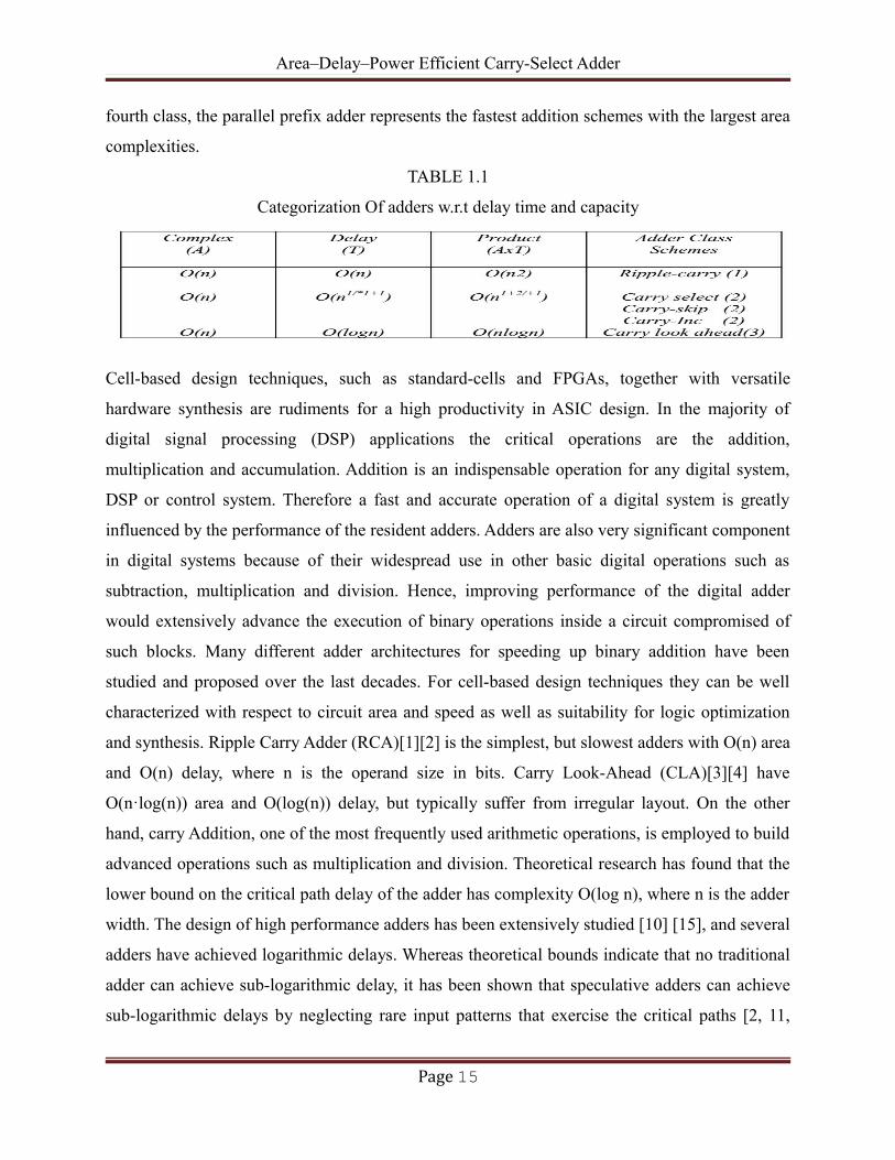
studied adder architectures. With respect to asymptotic delay time and area complexity, the
binary adder architectures can be categorized into four primary classes as given in Table 1.1. The
given results in the table are the highest exponent term of the exact formulas, very complex for
the high bit lengths of the operands.
The first class consists of the very slow ripple-carry adder with the smallest area. In the second
class, the carry-skip, carry-select adders with multiple levels have small area requirements and
shortened computation times. From the third class, the carry-look ahead adder and from the
Page 14
Area–Delay–Power Efficient Carry-Select Adder
fourth class, the parallel prefix adder represents the fastest addition schemes with the largest area
complexities.
TABLE 1.1
Categorization Of adders w.r.t delay time and capacity
Cell-based design techniques, such as standard-cells and FPGAs, together with versatile
hardware synthesis are rudiments for a high productivity in ASIC design. In the majority of
digital signal processing (DSP) applications the critical operations are the addition,
multiplication and accumulation. Addition is an indispensable operation for any digital system,
DSP or control system. Therefore a fast and accurate operation of a digital system is greatly
influenced by the performance of the resident adders. Adders are also very significant component
in digital systems because of their widespread use in other basic digital operations such as
subtraction, multiplication and division. Hence, improving performance of the digital adder
would extensively advance the execution of binary operations inside a circuit compromised of
such blocks. Many different adder architectures for speeding up binary addition have been
studied and proposed over the last decades. For cell-based design techniques they can be well
characterized with respect to circuit area and speed as well as suitability for logic optimization
and synthesis. Ripple Carry Adder (RCA)[1][2] is the simplest, but slowest adders with O(n) area
and O(n) delay, where n is the operand size in bits. Carry Look-Ahead (CLA)[3][4] have
O(n·log(n)) area and O(log(n)) delay, but typically suffer from irregular layout. On the other
hand, carry Addition, one of the most frequently used arithmetic operations, is employed to build
advanced operations such as multiplication and division. Theoretical research has found that the
lower bound on the critical path delay of the adder has complexity O(log n), where n is the adder
width. The design of high performance adders has been extensively studied [10] [15], and several
adders have achieved logarithmic delays. Whereas theoretical bounds indicate that no traditional
adder can achieve sub-logarithmic delay, it has been shown that speculative adders can achieve
sub-logarithmic delays by neglecting rare input patterns that exercise the critical paths [2, 11,
Page 15

Area–Delay–Power Efficient Carry-Select Adder
13]. Furthermore, by augmenting speculative adders with error detection and recovery, one can
construct reliable variable-latency adders whose average performance is very close to speculative
adders [3, 6, 12, and 17].
Speculative adders are built upon the observation that the critical path is rarely activated in
traditional adders. In traditional adders, each output depends on all previous (lower or equal
significance) bits. In particular, the most significant output depends on all the n bits, where n is
the adder width. In contrast, in speculative adders [2, 6, 11, 13, 17], each output only depends on
the previous k bits rather than all previous bits, where k is much smaller than n. However, the
cumulative error grows linearly with the adder width since each speculative output can
independently be in error. Moreover, the calculation of each speculative output requires an
individual k-bit adder; hence, such designs also incur large area overhead and large fanout at the
primary inputs. Techniques such as effective sharing [17] can mitigate but not eliminate fanout
and area problems. Although the speculative adder in [18] can mitigate the area problem, it
incurs a fairly high error rate that limits its application. For applications where errors cannot be
tolerated, a reliable variable latency adder can be built upon the speculative adder by adding
error detection and recovery [3, 6, 12, 17]. For the vast majority of input combinations, the
speculative adder produces correct results; when error detection flags an error, error recovery
provides correct results in one or more extra cycles. Ideally, the average performance of the
variable latency adder should be similar to the speculative one. However, existing variable
latency adders have several drawbacks. When error detection indicates no error, the actual delay
is the longer of the speculative adder and error detection. The delay of error detection is always
longer than the speculative adder [6] [17]. Hence, the benefit of speculation is limited by the
delay of error detection [3] [12]. Besides, the circuitry for error detection and recovery incurs
nontrivial area overhead. Finally, variable latency adders are mostly restricted for random inputs
[3, 12, and 17]. This thesis first describes a novel function speculation technique, called
speculative carry select addition (SCSA). The key idea is to segment the chain of propagate
signals in addition into blocks of the same size. Specifically, the input bits of addends are
segmented into blocks, and the carry bits between blocks are selectively truncated to 0. SCSA is
less susceptible to errors, since it is only applied for blocks instead of individual outputs. A single
individual adder is required to compute all outputs of a block instead of each output, which
mitigates the area overhead problem. An analytical model to determine the error rate of SCSA is
Page 16

Area–Delay–Power Efficient Carry-Select Adder
formulated, and the accurate relation between the block size and output error is developed. A
high performance speculative adder design is presented for low error rates (e.g. 0.01% and
0.25%). Secondly, this thesis describes a reliable variable latency adder design that augments the
speculative adder with error detection and recovery. The speculative adder produces correct
results in a single cycle in most cases, and error recovery provides correct results in an extra
cycle in worst cases. The performance of the variable latency adder is close to that of the
speculative adder. This approach has two advantages. First, the critical path delay of the error
detection block is lower or comparable to that of the speculative adder. Second, the error
detection and recovery circuitry incurs low area overhead by using intermediate results from the
speculative adder. Finally, the previous variable latency and speculative adders are mainly
designed for unsigned random inputs, so this thesis proposes the modified variable latency and
speculative adders suitable for both random and Gaussian inputs. With modified speculative
adder and error detection block, the variable latency adder still achieves high performance when
2's complement Gaussian inputs present. This shows that the variable latency adder design is
feasible for practical applications.
In the present work, the design of an 8-bit adder topology like ripple carry adder, carry look
ahead adder, carry skip adder, carry select adder, carry increment adder, carry save adder and
carry bypass adder are presented. It tightly integrates mixed-signal implementation with digital
implementation, circuit simulation, transistor-level extraction and verification. Performance
issues like area, power dissipation and propagation delay for all the adders are analyzed at
0.12µm 6metal layer CMOS technology using microwind tool. The remainder of this Project is
organized as follows.
Design of area and power-efficient high speed data path logic systems are one of the most
substantial areas of research in VLSI system design. In digital adders, the speed of addition is
limited by the time required to propagate a carry through the adder. The sum for each bit position
in an elementary adder is generated sequentially only after the previous bit position has been
summed and a carry propagated into the next position. The CSLA is used in many computational
systems to alleviate the problem of carry propagation delay by independently generating multiple
carries and then select a carry to generate the sum [1].
Page 17

Area–Delay–Power Efficient Carry-Select Adder
However, the CSLA is not area efficient because it uses multiple pairs of Ripple Carry Adders
(RCA) to generate partial sum and carry by considering carry input Cin = 0 and Cin = 1, then the
final sum and carry are selected by the multiplexers (mux).
The basic idea of this work is to use simple combinational circuit instead of RCA with cin = 1
and multiplexer in the regular CSLA to achieve lower area and power. The main advantage of
this Project is logic comes from low power than the n-bit Full Adder (FA) structure. The SQRT
CSLA has been developed by using simple combinational circuit and compared with regular
SQRT CSLA.
A regular CSLA uses two copies of the carry evaluation blocks, one with block carry input is
zero and other one with block carry input is one. Regular CSLA suffers from the disadvantage of
occupying more chip area. The modified CSLA reduces the area and power when compared to
regular CSLA with increase in delay by the use of Binary to Excess-1 converter. This Project
proposes a scheme which reduces the delay, area and power than regular and modified CSLA by
the use of D-latches.
Page 18

Area–Delay–Power Efficient Carry-Select Adder
CHAPTER-2
ADDER TOPOLOGIES
This section presents the design of adder topology. In this work the following adder structures
are used:
• Ripple Carry Adder
• Carry save Adder
• Carry Look-Ahead Adder
• Carry Increment adder
• Carry Skip Adder
• Carry Bypass Adder
• Carry Select Adder
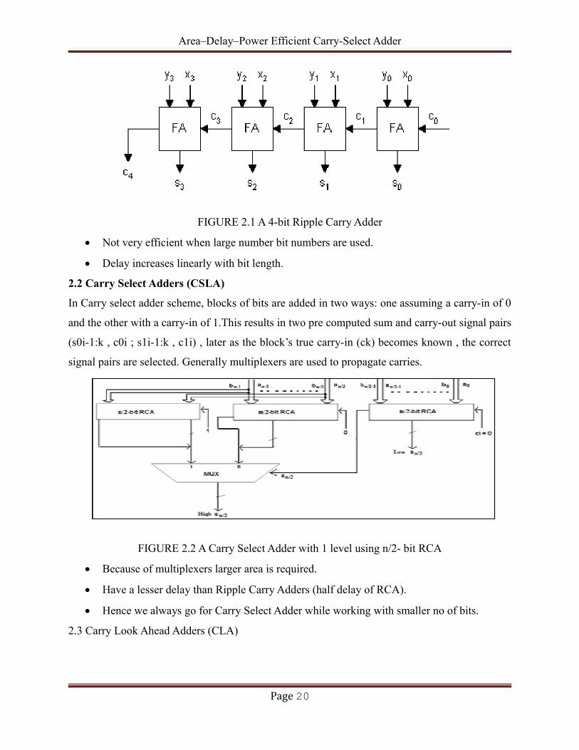
2.2 Ripple Carry Adder (RCA)
The ripple carry adder is constructed by cascading full adders (FA) blocks in series. One full
adder is responsible for the addition of two binary digits at any stage of the ripple carry. The
carryout of one stage is fed directly to the carry-in of the next stage. Even though this is a simple
adder and can be used to add unrestricted bit length numbers, it is however not very efficient
when large bit numbers are used. One of the most serious drawbacks of this adder is that the
delay increases linearly with the bit length. The worst-case delay of the RCA is when a carry
signal transition ripples through all stages of adder chain from the least significant bit to the most
significant bit, which is approximated by:
(1.1)
The well known adder architecture, ripple carry adder is composed of cascaded full adders for n-
bit adder, as shown in figure.1.It is constructed by cascading full adder blocks in series. The
carry out of one stage is fed directly to the carry-in of the next stage. For an n-bit parallel adder it
requires n full adders.
Page 19
Area–Delay–Power Efficient Carry-Select Adder
FIGURE 2.1 A 4-bit Ripple Carry Adder
Not very efficient when large number bit numbers are used.
Delay increases linearly with bit length.
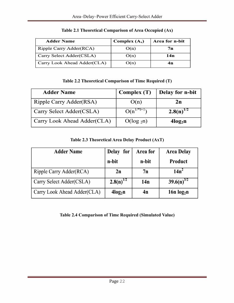
2.2 Carry Select Adders (CSLA)
In Carry select adder scheme, blocks of bits are added in two ways: one assuming a carry-in of 0
and the other with a carry-in of 1.This results in two pre computed sum and carry-out signal pairs
(s0i-1:k , c0i ; s1i-1:k , c1i) , later as the block’s true carry-in (ck) becomes known , the correct
signal pairs are selected. Generally multiplexers are used to propagate carries.
FIGURE 2.2 A Carry Select Adder with 1 level using n/2- bit RCA
Because of multiplexers larger area is required.
Have a lesser delay than Ripple Carry Adders (half delay of RCA).
Hence we always go for Carry Select Adder while working with smaller no of bits.
2.3 Carry Look Ahead Adders (CLA)
Page 20

Area–Delay–Power Efficient Carry-Select Adder
Carry Look Ahead Adder can produce carries faster due to carry bits generated in parallel by an
additional circuitry whenever inputs change. This technique uses carry bypass logic to speed up
the carry propagation.
FIGURE 2.3 4-BIT CLA Logic equations
Let ai and bi be the augends and addend inputs, ci the carry input, si and ci+1 , the sum and
carry-out to the ith bit position. If the auxiliary functions, pi and gi called the propagate and
generate signals, the sum output respectively are defined as follows.
As we increase the no of bits in the Carry Look Ahead adders, the complexity increases
because the no. of gates in the expression Ci+1 increases. So practically its not desirable
to use the traditional CLA shown above because it increase the Space required and the
power too.
Instead we will use here Carry Look Ahead adder (less bits) in levels to create a larger
CLA. Commonly smaller CLA may be taken as a 4-bit CLA. So we can define carry
look ahead over a group of 4 bits. Hence now we redefine terms carry generate as
[Group Generated Carry] g[ i,i+3 ] and carry propagate as [Group Propagated Carry]
p[ i,i+3 ] which are defined below.
2.4 ANALYSIS OF ADDERS
In our project we compared 3- different adders Ripple Carry Adders, Carry Select Adders and the
Carry Look Ahead Adders. The basic purpose of our experiment was to know the time and power
trade-offs between different adders whish will give us a clear picture of which adder suits best in
which type of situation during design process. Hence below we present both the theoretical and
practical comparisons of all the three adders whish were taken into consideration.
Page 21
Area–Delay–Power Efficient Carry-Select Adder
Table 2.1 Theoretical Comparison of Area Occupied (Ax)
Table 2.2 Theoretical Comparison of Time Required (T)
Table 2.3 Theoretical Area Delay Product (AxT)
Table 2.4 Comparison of Time Required (Simulated Value)
Page 22
Area–Delay–Power Efficient Carry-Select Adder
2.5 Binary to Excess-1 Converter:
In this work a binary to excess-1 code converter is achieved by using GDI technique for the
faster acceleration of the final addition in a hybrid adder. It is applied to the faster column
compression multiplication using a combination of two design techniques: partition of the partial
products into two parts for independent parallel column compression and acceleration of the
addition using hybrid adder. The performance of the proposed design is compared with CMOS
technology by evaluating the delay, power and transistor count with 180nm process technologies
on Tanner EDA tools. The results show the proposed design is significantly lower than CMOS
technology.
Code conversions are very essential in digital systems. Design of area and power efficient high
speed data path logic systems are one of the most substantial areas of research in VLSI system
design. In digital adders the speed of addition is limited by the time required to propagate a carry
through the adder. The sum for each bit position in an elementary adder is generated sequentially
only after the previous bit position has been summed and a carry propagated into the next
position. The CSLA is used in many computational systems to elevate the problem of carry
propagation delay. However the CSLA is not area efficient because it uses multiple pairs of
RCA(ripple carry adder) to generate partial sum and carry by considering carry input(Cin=0,
Cin=1), then final sum and carry are selected by multiplexers. The power and area of CSA can be
reduced by using BEC-1 converter instead of RCA.
In order to achieve efficient low power VLSI circuits we are illustrating a method of designing a
binary to Excess-1 code converter with GDI technique. A combinational circuit of adder with
multiplexer, binary to excess-1 code converter and ripple carry adder is called a Hybrid adder.
Page 23

Area–Delay–Power Efficient Carry-Select Adder
Here the binary to excess-1 converter has a complex layout using CMOS logic in terms of area,
delay and power consumption. Hence an attempt has been made to develop a converter for low
power consumption and less complexity.
The GDI method is based on the use of a simple cell. At first glance, the basic cell reminds one
of the standard CMOS inverter, but there are some important differences.
1) The GDI cell contains three inputs: G (common gate input of nMOS and pMOS), P (input to
the source/drain of pMOS), and N (input to the source/drain of nMOS).
2) Bulks of both nMOS and pMOS are connected to N or P (respectively), so it can be arbitrarily
biased at contrast with a CMOS inverter.
2.6. Existing system
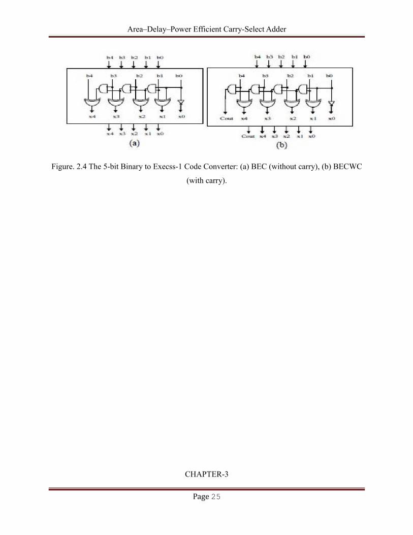
Code converters are very essential in digital systems. Here we are going to give the truth table
for binary to excess-1 converter.Excess-1 converter is obtained by adding one to the binary
value. The detailed structures of the 5-bit BEC without carry (BEC) and with carry (BECWC)
are shown in “Fig.2”. The BEC gets n inputs and generates n output; the BECWC gets n input
and generates n+1 output to give the carry output as the selection input of the next stage mux
used in the final adder design. The function table of BEC and BECWC are shown in Table III.
Table III
Truth table
Large bit sized multipliers requires multiple BEC and each of them requires the selection input
from the carry output of the preceding BEC.
Page 24
Area–Delay–Power Efficient Carry-Select Adder
Figure. 2.4 The 5-bit Binary to Execss-1 Code Converter: (a) BEC (without carry), (b) BECWC
(with carry).
CHAPTER-3
Page 25
Area–Delay–Power Efficient Carry-Select Adder
PROPOSED CONCEPT
RIPPLE CARRY ADDER
It is possible to create a logical circuit using multiple full adders to add N-bit numbers.
Each full adder inputs a Cin, which is the Cout of the previous adder. This kind of adder is a
ripple carry adder, since each carry bit "ripples" to the next full adder. Note that the first (and
only the first) full adder may be replaced by a half adder. The layout of a ripple carry adder is
simple, which allows for fast design time; however, the ripple carry adder is relatively slow,
since each full adder must wait for the carry bit to be calculated from the previous full adder. The
gate delay can easily be calculated by inspection of the full adder circuit. Each full adder
requires three levels of logic. One type of circuit where the effect of gate delays is particularly
clear is an ADDER. Thus, the Sum of the most significant bit is only available after the carry
signal has rippled through the adder from the least significant stage to the most significant stage.
This can be easily understood if one considers the addition of the two 4-bit words: (1 1 1 1)2 +
(0 0 0 1)2.
In this case, the addition of (1+1 = (10)2) in the least significant stage causes a carry bit to be
generated. This carry bit will consequently generate another carry bit in the next stage, and so on,
until the final carry-out bit appears at the output. This requires the signal to travel (ripple)
through all the stages of the adder. As a result, the final Sum and Carry bits will be valid after a
considerable delay. The carry-out bit of the first stage will be valid after 4 gate delays (2
associated with the XOR gate and 1 each associated with the AND and OR gates). one finds that
the next carry-out (C2) will be valid after an additional 2 gate delays (associated with the AND
and OR gates) for a total of 6 gate delays. In general the carry-out of a N-bit adder will be valid
after 2N+2 gate delays. The Sum bit will be valid an additional 2 gate delays after the carry-in
signal. Thus the sum of the most significant bit SN-1 will be valid after 2(N-1) + 2 +2 = 2N +2
gate delays. This delay may be in addition to any delays associated with interconnections. It
should be mentioned that in case one implements the circuit in a FPGA, the delays may be
different from the above expression depending on how the logic has been placed in the look up
tables and how it has been divided among different CLBs.
6.1 HALF ADDER
The half adder is an example of a simple, functional digital circuit built from two logic
gates. A half adder adds two one-bit binary numbers A and B. It has two outputs, S and C (the
Page 26
Area–Delay–Power Efficient Carry-Select Adder
value theoretically carried on to the next addition); the final sum is 2C + S. The simplest half-
adder design, pictured on the right, incorporates an XOR gate for S and an AND gate for C. Half
adders cannot be used compositely, given their incapacity for a carry-in bit.
6.2 FULL ADDER
A full adder adds binary numbers and accounts for values carried in as well as out. A one-
bit full adder adds three one-bit numbers, often written as A, B, and Cin.A and B are the
operands, and Cin is a bit carried in (in theory from a past addition). The full-adder is usually a
component in a cascade of adders, which add 8, 16, 32, etc. binary numbers. The circuit produces
a two-bit output sum typically represented by the signals Cout and S, where. The one-bit full
adder's truth table is:
BINARY TO EXCESS-1 CONVERTER
The main idea of this work is to use BEC instead of the RCA with Cin = 1 in order to
reduce the area and power consumption of the regular CSLA. To replace the n-bit RCA, an n+1-
bit BEC is required. A structure and the function table of a 4-b BEC. Illustrates how the basic
function of the CSLA is obtained by using the4-bit BEC together with the mux. One input of the
2:1 mux gets as it input(B3, B2, B1, and B0) and another input of the mux is the BEC output.
This produces the two possible partial results in parallel and the mux is used to select either the
BEC output or the direct inputs according to the control signal Cin. The importance of the BEC
logic stems from the large silicon area reduction when the CSLA with large number of bits are
designed.
The Boolean expressions of the 4-bit BEC is listed as (note the functional symbols ~
NOT, & AND, ^ XOR)
X0 = ~B0
X1 = B0 ^ B1
X2 = B2 ^ (B0& B1)
X3 = B3 ^ (B0 & B1& B2).
The 4-bit BEC with 2:1 multiplexer, the inputs for the 2:1MUX are one is the output of the 4-bit
BEC and another input is output of 4- bit full adder with input carry equal to zero. The selection
line is carry of previous stage which select one of the input as output, if Cin=1 output is 4-bit
BEC output.
Page 27
Area–Delay–Power Efficient Carry-Select Adder
MULTIPLEXER
In electronics, a multiplexer (or MUX) is a device that selects one of several analog or
digital input signals and forwards the selected input into a single line. multiplexer of 2n inputs
has n select lines, which are used to select which input line to send to the output. Multiplexers
are mainly used to increase the amount of data that can be sent over the network within a certain
amount of time and bandwidth. A multiplexer is also called a data selector. An electronic
multiplexer makes it possible for several signals to share one device or resource, for example one
A/D converter or one communication line, instead of having one device per input signal.
In digital circuit design, the selector wires are of digital value. In the case of a 2-to-1
multiplexer, a logic value of 0 would connect to the output while a logic value of 1 would
connect to the output. In larger multiplexers, the number of selector pins is equal to where is the
number of inputs. A 2-to-1 multiplexer has a Boolean equation where and are the two inputs, is
the selector input, and is the output:
VLSI stands for Very large scale integration which refers to those integrated circuits that contain
more than 107transistors. Designing such circuit is difficult and that design needs to overcome
the VLSI design problem like Area, Speed, Power dissipation, Design time and Testability. In
digital adders, the speed of addition is limited by the time required to propagate a carry through
the adder. The sum for each bit position in an elementary adder is generated sequentially only
after the previous bit position has been summed and a carry propagated into the next position.
The early years carry look ahead adder used to overcome the delay it will produce all produce all
the carries at time but it requires more circuitry, next those are replaced by carry select adders
using dual RCAs. In this sum is generated for Cin=1 and Cin=0, depends on input carry one sum
is passed as final sum using multiplexer. The problem is again, it requires more circuitry because
it requires two full adders at each stage of three bits addition. That is replaced by one RCA and
one add-one circuit. There again the same problem that is eliminated by this proposed system
CSLA using BEC. The basic idea of this work is to use Binary to Excess-1 Converter (BEC)
instead of RCA with Cin = 1 in the regular CSLA to achieve lower area and power consumption.
The main advantage of this BEC logic comes from the lesser number of logic gates than
the n-bit Full Adder (FA) structure. The carry-select adder generally consists of two ripple carry
adders and a multiplexer. Adding two n-bit numbers with a carry-select adder is done with two
adders (therefore two ripple carry adders) in order to perform the calculation twice, one time
Page 28

Area–Delay–Power Efficient Carry-Select Adder
with the assumption of the carry being zero and the other assuming one. After the two results are
calculated, the correct sum, as well as the correct carry, is then selected with the multiplexer once
the correct carry is known. The number of bits in each carry select block can be uniform, or
variable. In the uniform case, the optimal delay occurs for a block size of n variable, the block
size should have a delay, from additional inputs A and B to the carry out, equal to that of the
multiplexer chain leading into it, so that the carry out is calculated just in time. The delay is
derived from uniform sizing, where the ideal number of full-adder elements per block is equal to
the square root of the number of bits being added, since that will yield an equal number of MUX
delays.
Two 4-bit ripple carry adders are multiplexed together, where the resulting carry and sum
bits are selected by the carry-in. Since one ripple carry adder assumes a carry-in of 0, and the
other assumes a carry-in of 1, selecting which adder had the correct assumption via the actual
carry-in yields the desired result. A 16-bit carry-select adder
with a uniform block size of 4 can be created with three of these blocks and a 4-bit ripple carry
adder. Since carry-in is known at the beginning of computation, a carry select block is not needed
for the first four bits. The delay of this adder will be four full adder delays, plus three MUX
delays A 32-bit carry-select adder with variable size can be similarly created. Here we show an
adder with block sizes. This break-up is ideal when the full-adder delay is equal to the MUX
delay, which is unlikely. The total delay is two full adder delays, and four MUX delays. Addition
is the heart of computer arithmetic, and the arithmetic unit is often the work horse of a
computational circuit. They are the necessary component of a data path, e.g. in microprocessors
or a signal processor. There are many ways to design an adder.
The Ripple Carry Adder (RCA) provides the most compact design but takes longer
computing time. If there is N-bit RCA, the delay is linearly proportional to N. Thus for large
values of N the RCA gives highest delay of all adders. The Carry Look Ahead Adder (CLA)
gives fast results but consumes large area. If there is N-bit adder, CLA is fast for N≤4, but for
large values of N its delay increases more than other adders. So for higher number of bits, CLA
gives higher delay than other adders due to presence of large number of fan-in and a large
number of logic gates. The Carry Select Adder (CSA) provides a compromise between small area
but longer delay RCA and a large area with shorter delay CLA. In rapidly growing mobile
industry, faster units are not the only concern but also smaller area and less power become major
Page 29

Area–Delay–Power Efficient Carry-Select Adder
concerns for design of digital circuits. In mobile electronics, reducing area and power
consumption are key factors in increasing portability and battery life. Even in servers and
desktop computers power dissipation is an important design constraint. Design of area- and
power-efficient high-speed data path logic systems are one of the most substantial areas of
research in VLSI system design. In digital adders, the speed of addition is limited by the time
required to propagate a carry through the adder.
3.1 BLOCK DIAGRAM FOR REGULAR CSLA
Figure: 3.1 Block diagram of regular CSLA
3.2 BLOCK DIAGRAM OF MODIFIED CSLA
Figure: 3.2 Block diagram of modified CSLA.
OPERATION
Page 30
Area–Delay–Power Efficient Carry-Select Adder
Carry Select Adders (CSA) is one of the fastest adders used in many data-processing processors
to perform fast arithmetic functions. The carry-select adder partitions the adder into several
groups, each of which performs two additions in parallel. Therefore, two copies of ripple-carry
adder act as carry evaluation block per select stage. One copy evaluates the carry chain assuming
the block carry-in is zero, while the other assumes it to be one. Once the carry signals are finally
computed, the correct sum and carry-out signals will be simply selected by a set of multiplexers.
The 4-bit adder block is RCA. Systems are one of the most substantial areas of research in VLSI
system design. In digital adders, the speed of addition is limited by the time required to
propagate a carry through the adder. The sum for each bit position in an elementary adder is
generated sequentially only after the previous bit position has been summed and a carry
propagated into the next position. The CSLA is used in many computational systems to alleviate
the problem of carry propagation delay by independently generating multiple carries and then
select a carry to generate the sum. However, the CSLA is not area efficient because it uses
multiple pairs of Ripple Carry Adders (RCA) to generate partial sum and carry by considering
carry input and, then the final sum and carry are selected by the multiplexers (MUX).
The carry-select adder generally consists of two ripple carry adders and a multiplexer.
Adding two n-bit numbers with a carry-select adder is done with two adders (therefore two ripple
carry adders) in order to perform the calculation twice, one time with the assumption of the carry
being zero and the other assuming one. After the two results are calculated, the correct sum, as
well as the correct carry, is then selected with the multiplexer once the correct carry is known.
The number of bits in each carry select block can be uniform, or variable. In the uniform case,
the optimal delay occurs for a block size of n variable, the block size should have a delay, from
additional inputs A and B to the carry out, equal to that of the multiplexer chain leading into it, so
that the carry out is calculated just in time. The delay is derived from uniform sizing,where the
ideal number of full-adder elements per block is equal to the square root of the number of bits
being added, since that will yield an equal number of MUX delays. Two 4-bit ripple carry adders
are multiplexed together, where the resulting carry and sum bits are selected by the carry-in.
Since one ripple carry adder assumes a carry-in of 0, and the other assumes a carry-in of 1,
selecting which adder had the correct assumption via the actual carry-in yields the desired result.
A 16-bit carry-select adder with a uniform block size of 4 can be created with three of these
blocks and a 4-bit ripple carry adder. Since carry-in is known at the beginning of computation, a
Page 31

Area–Delay–Power Efficient Carry-Select Adder
carry select block is not needed for the first four bits. The delay of this adder will be four full
adder delays, plus three MUX delays. A 16-bit carry-select adder with variable size can be
similarly created. Here we show an adder with block sizes. This break-up is ideal when the full-
adder delay is equal to the MUX delay, which is unlikely. The total delay is two full adder
delays, and four MUX delays.
Addition is the heart of computer arithmetic, and the arithmetic unit is often thework
horse of a computational circuit. They are the necessary component of a data path, e.g. in
microprocessors or a signal processor. There are many ways to design an added. The Ripple
Carry Adder (RCA) provides the most compact design but takes longer computing time. If there
is N-bit RCA, the delay is linearly proportional to N. Thus for large values of N the RCA gives
highest delay of all adders. The Carry Look Ahead Adder (CLA) gives fast results but consumes
large area. If there is N-bit adder, CLA is fast for N≤4, but for large values of N its delay
increases more than other adders. So for higher number of bits, CLA gives higher delay than
other adders due to presence of large number of fan-in and a large number of logic gates. The
Carry Select Adder (CSA) provides a compromise between small area but longer delay RCA and
a large area with shorter delay CLA. In rapidly growing mobile industry, faster units are not the
only concern but also smaller area and less power become major concerns for design of digital
circuits. In mobile electronics, reducing area and power consumption are key factors in
increasing portability and battery life. Even in servers and desktop computers power dissipation
is an important design constraint. Design of area- and power-efficient high-speed data path logic
systems are one of the most substantial areas of research in VLSI system design. In digital
adders, the speed of addition is limited by the time required to propagate a carrythrough the
adder. The sum for each bit position in an elementary adder is generated sequentially only after
the previous bit position has been summed and a carry propagated into the next position. Among
various adders, the CSA is intermediate regarding speed and area.
WHY WE REPLACED REGULAR CSLA WITH MODIFIED CSLA?
Regular CSLA has 2 ripple carry adders (rca) in each module for performing addition
depending on carry.
Using 2 RCAsin each module increases the number of transistors.
Increase in number of transistors leads to increase in area and power consumption.
Page 32

Area–Delay–Power Efficient Carry-Select Adder
2nd RCA in each module can be replaced by binary to excess one converter which performs
the same operation with less number of transistors which leads to modified CSLA which is
area efficient and low power consumption
CHAPTER-4
PROPOSED CONCEPT
4.1 INTRODUCTION
Low-Power, area-efficient, and high-performance VLSI systems are increasingly used in portable
and mobile devices, multi standard wireless receivers, and biomedical instrumentation [1], [2].
An adder is the main component of an arithmetic unit. A complex digital signal processing (DSP)
system involves several adders. An efficient adder design essentially improves the performance
of a complex DSP system. A ripple carry adder (RCA) uses a simple design, but carry
propagation delay (CPD) is the main concern in this adder. Carry look-ahead and carry select
(CS) methods have been suggested to reduce the CPD of adders. A conventional carry select
adder (CSLA) is an RCA–RCA configuration that generates a pair of sum words and output
carry bits corresponding the anticipated input-carry (cin = 0 and 1) and selects one out of each
pair for final-sum and final-output-carry [3]. A conventional CSLA has less CPD than an RCA,
but the design is not attractive since it uses a dual RCA. Few attempts have been made to avoid
dual use of RCA in CSLA design. Kim and Kim [4] used one RCA and one add-one circuit
instead of two RCAs, where the add-one circuit is implemented using a multiplexer (MUX). He
et al. [5] proposed a square-root (SQRT)-CSLA to implement large bit-width adders with less
delay. In a SQRT CSLA, CSLAs with increasing size are connected in a cascading structure. The
main objective of SQRT-CSLA design is to provide a parallel path for carry propagation that
Page 33

Area–Delay–Power Efficient Carry-Select Adder
helps to reduce the overall adder delay. We suggested a binary to BEC-based CSLA. The BEC-
based CSLA involves less logic resources than the conventional CSLA, but it has marginally
higher delay. A CSLA based on common Boolean logic (CBL) is also proposed in [7] and [8].
The CBL-based CSLA of [7] involves significantly less logic resource than the conventional
CSLA but it has longer CPD, which is almost equal to that of the RCA. To overcome this
problem, a SQRT-CSLA based on CBL was proposed in [8]. However, the CBL-based
SQRTCSLA design of [8] requires more logic resource and delay than the BEC-based SQRT-
CSLA of [6]. We observe that logic optimization largely depends on availability of redundant
operations in the formulation, whereas adder delay mainly depends on data dependence. In the
existing designs, logic is optimized without giving any consideration to the data dependence. In
this brief, we made an analysis on logic operations involved in conventional and BEC-based
CSLAs to study the data dependence and to identify redundant logic operations. Based on this
analysis, we have proposed a logic formulation for the CSLA.
The main contribution in this brief is logic formulation based on data dependence and optimized
carry generator (CG) and CS design. Based on the proposed logic formulation, we have derived
an efficient logic design for CSLA. Due to optimized logic units, the proposed CSLA involves
significantly less ADP than the existing CSLAs. We have shown that the SQRT-CSLA using the
proposed CSLA design involves nearly 32% less ADP and consumes 33% less energy than that
of the corresponding SQRT-CSLA.
4.2 LOGIC FORMULATION
The CSLA has two units: 1) the sum and carry generator unit (SCG) and 2) the sum and carry
selection unit [9]. The SCG unit consumes most of the logic resources of CSLA and significantly
contributes to the critical path. Different logic designs have been suggested for efficient
implementation of the SCG unit. We made a study of the logic designs suggested for the SCG
unit of conventional and BEC-based CSLAs of [6] by suitable logic expressions. The main
objective of this study is to identify redundant logic operations and data dependence.
Accordingly, we remove all redundant logic operations and sequence logic operations based on
their data dependence.
Page 34

Area–Delay–Power Efficient Carry-Select Adder
Fig. 4.1. (a) Conventional CSLA; n is the input operand bit-width. (b) The logic operations of the
RCA is shown in split form, where HSG, HCG, FSG, and FCG represent half-sum generation,
half-carry generation, full-sum generation, and full-carry generation, respectively.
4.2.1 Logic Expressions of the SCG Unit of the
Conventional CSLA As shown in Fig. 4.1(a), the SCG unit of the conventional CSLA [3] is
composed of two n-bit RCAs, where n is the adder bit-width. The logic operation of the n-bit
RCA is performed in four stages: 1) half-sum generation (HSG); 2) half-carry generation (HCG);
3) full-sum generation (FSG); and 4) full carry generation (FCG). Suppose two n-bit operands
are added in the conventional CSLA, then RCA-1 and RCA-2 generate n-bit sum (s0 and s1) and
output-carry (c0 out and c1 out) corresponding to input-carry (cin = 0 and cin = 1), respectively.
Logic expressions of RCA-1 and RCA-2 of the SCG unit of the n-bit CSLA are given as
(4.1)
4.2.2 Logic Expression of the SCG Unit of the BEC-Based CSLA
Page 35

Area–Delay–Power Efficient Carry-Select Adder
Fig.4.2. Structure of the BEC-based CSLA; n is the input operand bit-width.
As shown in Fig. 4.2, the RCA calculates n-bit sum and corresponding to cin = 0. The BEC unit
receives and from the RCA and generates (n + 1)-bit excess-1 code. The most significant bit
(MSB) of BEC represents c1 out, in which n least significant bits (LSBs) represent . The logic
expressions
(4.2)
We can find from 4.2 that, in the case of the BEC-based CSLA, depends on, which otherwise
has no dependence on in the case of the conventional CSLA.
The BEC method therefore increases data dependence in the CSLA. We have considered logic
expressions of the conventional CSLA and made a further study on the data dependence to find
an optimized logic expression for the CSLA. It is interesting to note from 4.2 that logic
expressions of and are identical except the terms and since (= = s0). In addition, we find that
and depend on {s0, c0, cin}, where c0 = =. Since and have no dependence on and, the logic
operation of and can be scheduled before and, and the select unit can select one from the set (s0
1, s1 1) for the final-sum of the CSLA. We find that a significant amount of logic resource is
spent for calculating {,}, and it is not an efficient approach to reject one sum-word after the
calculation. Instead, one can select the required carry word from the anticipated carry words {c0
and c1} to calculate the final-sum. The selected carry word is added with the half-sum (s0) to
generate the final-sum (s). Using this method, one can have three design advantages:
Page 36

Area–Delay–Power Efficient Carry-Select Adder
1) Calculation of s0 1 is avoided in the SCG unit;
2) The n-bit select unit is required instead of the (n + 1) bit; and
3) Small output-carry delay. All these features result in an area–delay and energy-efficient design
for the CSLA.
We have removed all the redundant logic operations of 4.2 and rearranged logic expressions of
4.2based on their dependence. The proposed logic formulation for the CSLA is given as
(4.3)
4.3 PROPOSED ADDER DESIGN
Fig. 4.3. (a) Proposed CS adder design, where n is the input operand bit-width, and [∗] represents
delay (in the unit of inverter delay), n = max (t, 3.5n + 2.7). (b) Gate-level design of the HSG. (c)
Page 37

Area–Delay–Power Efficient Carry-Select Adder
Gate-level optimized design of (CG0) for input-carry = 0. (d) Gate-level optimized design of
(CG1) for input-carry = 1. (e) Gate-level design of the CS unit. (f) Gate-level design of the final-
sum generation (FSG) unit.
The proposed CSLA is based on the logic formulation given in 4.3, and its structure is shown in
Fig. 4.3(a). It consists of one HSG unit, one FSG unit, one CG unit, and one CS unit. The CG
unit is composed of two CGs (CG0 and CG1) corresponding to input-carry ‘0’ and ‘1’. The HSG
receives two n-bit operands (A and B) and generate half-sum word s0 and half-carry word c0 of
width n bits each. Both CG0 and CG1 receive s0 and c0 from the HSG unit and generate two n-
bit full-carry words c0 1 and c11 corresponding to input-carry ‘0’ and ‘1’, respectively.
The logic diagram of the HSG unit is shown in Fig. 3(b). The logic circuits of CG0 and CG1 are
optimized to take advantage of the fixed input-carry bits. The optimized designs of CG0 and
CG1 are shown in Fig. 4.3(c) and (d), respectively.
The CS unit selects one final carry word from the two carry words available at its input line
using the control signal cin. It selects when cin = 0; otherwise, it selects . The CS unit can be
implemented using an n-bit 2-to-l MUX. However, we find from the truth table of the CS unit
that carry words c0 1 and c11 follow a specific bit pattern. If (i) = ‘1’, then (i) = 1, irrespective
of s0(i) and c0(i), for 0 ≤ i ≤ n − 1. This feature is used for logic optimization of the CS unit. The
optimized design of the CS unit is shown in Fig. 3(e), which is composed of n AND–OR gates.
The final carry word c is obtained from the CS unit. The MSB of c is sent to output as cout, and
(n − 1) LSBs are XORed with (n − 1) MSBs of half-sum (s0) in the FSG [shown in Fig. 3(f)] to
obtain (n − 1) MSBs of final-sum (s). The LSB of s0 is XORed with cin to obtain the LSB of s.
4.4 PERFORMANCE COMPARISON
4.4.1 Area–Delay Estimation Method
We have considered all the gates to be made of 2-input AND, 2-input OR, and inverter (AOI). A
2-input XOR is composed
TABLE I
AREA AND DELAY OF AND, OR, AND NOT GATES GIVEN IN THE SAED
90-nm STANDARD CELL LIBRARY DATASHEET
Page 38

Area–Delay–Power Efficient Carry-Select Adder
of 2 AND, 1 OR, and 2 NOT gates. The area and delay of the 2-input AND, 2-input OR, and
NOT gates (shown in Table I) are taken from the Synopsys Armenia Educational Department
(SAED) 90-nm standard cell library datasheet for theoretical estimation. The area and delay of a
design are calculated using the following relations:
(4.4)
where (Na, No, Ni) and (na, no, ni), respectively, represent the (AND, OR, NOT) gate counts of
the total design and its critical path. (a, r, i) and (Ta, To, Ti), respectively, represent the area and
delay of one (AND, OR, NOT) gate. We have calculated the (AOI) gate counts of each design
for area and delay estimation. Using (5a) and (5b), the area and delay of each design are
calculated from the AOI gate counts (Na, No, Ni), (na, no, ni), and the cell details of Table I.
where (Na, No, Ni) and (na, no, ni), respectively, represent the (AND, OR, NOT) gate counts of
the total design and its critical path. (a, r, i) and (Ta, To, Ti), respectively, represent the area and
delay of one (AND, OR, NOT) gate. We have calculated the (AOI) gate counts of each design for
area and delay estimation. Using (5a) and (5b), the area and delay of each design are calculated
from the AOI gate counts (Na, No, Ni), (na, no, ni), and the cell details of Table I. path of the
proposed CSLA, the delay of each intermediate and output signals of the proposed n-bit CSLA
design of Fig. 3 is shown in the square bracket against each signal. We can find from Table II that
the proposed n-bit single-stage CSLA adder involves 6n less number of AOI gates than the
CSLA of [6] and takes 2.7 and 6.6 units less delay to calculate final-sum and output-carry.
Compared with the CBL-based CSLA of [7], the proposed CSLA design involves n more AOI
gates, and it takes (n − 4.7) unit less delay to calculate the output-carry.
Using the expressions of Table II and AOI gate details of Table I, we have estimated the area and
delay complexities of the proposed CSLA and the existing CSLA of [6]–[8], including the
Page 39
Area–Delay–Power Efficient Carry-Select Adder
conventional one for input bit-widths 8 and 16. For the single-stage CSLA, the input-carry delay
is assumed to be t = 0 and the delay of final-sum (fs) represents the adder delay. The estimated
values are listed in Table III for comparison. We can find from Table III that the proposed
CSLA involves nearly 29% less area and 5% less output delay than that of [6]. Consequently, the
CSLA of [6] involves 40% higher ADP than the proposed CSLA, on average, for different bit-
widths. Compared with the CBL-based CSLA of [7], the proposed CSLA design has marginally
less ADP.
However, in the CBL-based CSLA, delay increases at a much higher rate than the proposed
CSLA design for higher bit widths. Compared with the conventional CSLA, the proposed CSLA
involves 0.42 ns more delay, but it involves nearly 28% less ADP due to less area complexity.
Interestingly, the proposed CSLA design offers multipath parallel carry propagation whereas the
CBL-based CSLA of [7] offers a single carry propagation path identical to the RCA design.
Moreover, the proposed CSLA design has 0.45 ns less output-carry delay than the output-sum
delay. This is mainly due to the CS unit that produces output-carry before the FSG calculates the
final-sum.
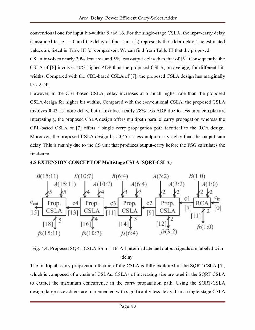
4.5 EXTENSION CONCEPT OF Multistage CSLA (SQRT-CSLA)
Fig. 4.4. Proposed SQRT-CSLA for n = 16. All intermediate and output signals are labeled with
delay
The multipath carry propagation feature of the CSLA is fully exploited in the SQRT-CSLA [5],
which is composed of a chain of CSLAs. CSLAs of increasing size are used in the SQRT-CSLA
to extract the maximum concurrence in the carry propagation path. Using the SQRT-CSLA
design, large-size adders are implemented with significantly less delay than a single-stage CSLA
Page 40

Area–Delay–Power Efficient Carry-Select Adder
of same size. However, carry propagation delay between the CSLA stages of SQRT-CSLA is
critical for the overall adder delay. Due to early generation of output-carry with multipath carry
propagation feature, the proposed CSLA design is more favorable than the existing CSLA
designs for area–delay efficient implementation of SQRT-CSLA. A 16-bit SQRT-CSLA design
using the proposed CSLA is shown in Fig. 4.4, where the 2-bit RCA, 2-bit CSLA, 3-bit CSLA,
4-bit CSLA, and 5-bit CSLA are used. We have considered the cascaded configuration of (2-bit
RCA and 2-, 3-, 4-, 6-, 7-, and 8-bit CSLAs) and (2-bit RCA and 2-, 3-, 4-, 6-, 7-, 8-, 9-, 11-, and
12-bit CSLAs), respectively, for the 32-bit SQRTCSLA and the 64-bit SQRT-CSLA to optimize
adder delay. To demonstrate the advantage of the proposed CSLA design in SQRT-CSLA, we
have estimated the area and delay of SQRTCSLA using the proposed CSLA design and the BEC-
based CSLA of [6] and the CBL-based CSLA of [7] for bit-widths 16, 32, and 64.
CHAPTER-5
SOFTWARE TOOLS
5.1 Introduction to FPGA’s:
Field programmable gate arrays ( FPGA ) are a class of general purpose devices that can
be configured for a wide variety of applications. Field programmable gate arrays were first
Page 41
Area–Delay–Power Efficient Carry-Select Adder
introduced by Xilinx in the mid-1980’s. Before the availability of FPGA ’s, a designer had the
options for implementing digital logic in dis crete logic devices (VLSI or SSI), programmable
devices (PAL ’s or PLD ’s), and cell-based Application Specific Integrated Circuits ( ASIC ’s ).
At this stage it is necessary to see the difference between an ASIC and an FPGA and determine
the need to carry out the implementation of the circuit in FPGA ’s. Up to this point in this thesis,
what was presented was more of a custom hardware circuit design-- often known as application
specific integrated circuits. ASIC ’s provide the exact functionality required for a specific task .
They are smaller, faster, cheaper and consume less power than a programmable processor and
will solve the specific problem for which it was designed. But in a situation where we would
require a slightly modified alternative to the developed ASIC the approach would probably
require rebuilding the entire chip which would be both costly and time consuming. It is in such a
situation that FPGA ’s could come into play. A discrete device can be used to implement a small
amount of logic, while a programmable device, by comparison, is a general-purpose device
capable of implementing extremely large logic . The flexibility here is that it is capable of being
programmed by the users at their site using programming hardware. Hence, FPGA’ s provide the
benefits of custom VLSI, while avoiding the initial cost and time delay associated with ASIC
design. They allow the implementation of integrated digital electronic circuits without requiring
the complex approach used in a conventional chip fabrication. These are highly tuned hardware
circuits that can be modified at any point during use and consist of configurable logic blocks
( CLB ’s ) which implement the logical functions of gates. This architecture would be discussed
in the next section. In FPGA ’s, the logic function performed within the logic blocks as well as
the interconnections between the blocks can be programmed repeatedly, and this configuration
within the chip can be accomplished in a few milliseconds. ASIC ’s definitely have their
advantages over FPGA ’s, but FPGA ’s are highly recommended where time and money are a
factor. In fact, the field programmable gate array is the preferred first step into application
specific integrated circuits. In order to clearly illustrate the above discussion with a simple
example, imagine yourself on a warship in the middle of an ocean. The ship obviously has a
great deal of sophisticated equipment built using a number of important IC’s. When such an IC
fails to perform its desired task and the ship does not happen to have a stock of the required
chips, it obviously would be extremely beneficial to program an FPGA and use it in place of the
custom IC rather than the ship returning to the dock for the device. 5.2 Architecture ( Xilinx
Page 42
Area–Delay–Power Efficient Carry-Select Adder
4000 series FPGA ) In the FPGA ’s the architecture and technology determine the methods of
interconnections and programming. The most important technologies are
1. SRAM technology
2. Anti-fuse technology
3. EPROM/EEPROM technology
5.1.1 SRAM Technology
In the static RAM technology, programmable interconnections are made using pass
transistors, transmission gates or multiplexers that are controlled by SRAM cells. The advantage
is that it allows fast in circuit reconfiguration. 2. Anti-Fuse Technology In this technology an
anti-fuse resides in high impedence and can be programmed into low impedence or fused state.
3. EPROM/EEPROM Technology This concept is similar to that used in EPROM memories. In
this technology there is no necessity for an external storage of the configuration. The FPGA used
in this thesis which is the Xilinx XC4010XLPC84 is SRAM based. The major building blocks in
an FPGA are
1. Configurable Logic Blocks ( CLB ’s).
2. Input /Output Blocks ( IOB ’s ).
3. Programmable interconnects.
Page 43

Area–Delay–Power Efficient Carry-Select Adder
Fig 5.1 – FPGA architecture:
Xilinx FPGA’s consisted of a matrix of logic cells or the above mentioned CLB ’s
surrounded by vertical and horizontal channels of programmable interconnects and the periphery
being surrounded by IOB ’s. A basic block diagram of this architecture is shown above.
FPGA ’s that are fine grained structure have large number of simple CLB ’s while those
with coarse grained structure have smaller number of powerful blocks. 5.2.1 Configurable Logic
Blocks Each CLB contains of a pair of flips and two independent four input function generators.
The flip flops are accessed through the thirteen inputs and four outputs of the configurable logic
blocks. The configurable logic blocks are responsible for implementing most of the logic in an
FPGA. A third function generator is also available and has three inputs. One or two of these
inputs can be the outputs from the other two function generators while the other input(s) are from
outside the CLB.
Hence each CLB would be capable of implementing functions of up to nine variables.
The outputs from these function generators are stored in flip-flops within the CLB. Implementing
large functions in a single CLB would reduce the number of cells needed and the delay
associated therefore resulting in both area and speed efficiency. 5.2.2 Input / Output Blocks The
Page 44
Area–Delay–Power Efficient Carry-Select Adder
input/output blocks in an FPGA provide interface between the external package pins and the
internal logic. Each IOB is defined as either as an input, an output or a bidirectional signal. Here
two paths are responsible for bringing the input signals into the array and also connect to an
input register that is capable of being programmed either as an edge-triggered flop-flop or as a
level sensitive latch. The inputs can be globally configured for either TTL or CMOS logic.
Programmable interconnects internally the connection are achieved using metal
segments with programmable switching points. These switching points or switching matrices
basically consists of six pass transistors that can turned on and off to provide the desired routing.
The major interconnections within the FPGA are provided by single length lines which are
vertical lines that intersect at a switch matrix, double length lines which are twice as long as the
single length lines and long lines that run the entire length or width of the array of cells. The
various interconnections inside an FPGA are made using these routing channels. CLB outputs are
routed to the long lines through tri-state buffers or the single length interconnect lines. In
addition there is also a routing resource around the IOB known as the versa ring which facilitates
the swapping of the pins and facilitates redesign.
5.2 History Evolution of Programmable Logic Devices:
The first type of user-programmable chip that could implement logic circuits was the
Programmable Read-Only Memory (PROM), in which address lines can be used as logic circuit
inputs andData lines as outputs. Logic functions, however, rarely require more than a few
product terms, and A PROM contains a full decoder for its address inputs. PROMS are thus an
inefficient architecture For realizing logic circuits, and so are rarely used in practice for that
purpose. The first device Developed later specifically for implementing logic circuits was the
Field-Programmable Logic Array (FPLA), or simply PLA for short. A PLA consists of two levels
of logic gates.
Mable “wired” AND-plane followed by a programmable “wired” OR-plane. A PLA is
structured So that any of its inputs (or their complements) can be Ended together in the AND-
plane; each AND-plane output can thus correspond to any product term of the inputs. Similarly,
each OR plane Output can be configured to produce the logical sum of any of the AND-plane
Page 45

Area–Delay–Power Efficient Carry-Select Adder
outputs. With This structure, PLAs are well-suited for implementing logic functions in sum-of-
products form.
They are also quite versatile, since both the AND terms and OR terms can have many
inputs (this Feature is often referred to as wide AND and OR gates). When PLAs were
introduced in the early 1970s, by Philips, their main drawbacks were that They were expensive to
manufacture and offered somewhat poor speed-performance. Both disadvantages Were due to the
two levels of configurable logic, because programmable logic planes Were difficult to
manufacture and introduced significant propagation delays. To overcome these Weaknesses,
Programmable Array Logic (PAL) devices were developed. As Figure 1 illustrates, PALs feature
only a single level of programmability, consisting of a programmable “wired” AND plane That
feeds fixed OR-gates. To compensate for lack of generality incurred because the OR- Outputs
Figure 5.2 Structure Of Pal
Plane is fixed, several variants of PALs are produced, with different numbers of inputs and
outputs,And various sizes of OR-gates. PALs usually contain flip-flops connected to the OR-gate
outputs So that sequential circuits can be realized. PAL devices are important because when
introduced they had a profound effect on digital hardware design, and also they are the basis for
Some of the newer, more sophisticated architectures that will be described shortly. Variants of the
Basic PAL architecture is featured in several other products known by different
acronyms. All Small PLDs, including PLAs, PALs, and PAL-like devices are grouped into a
single category Called Simple PLDs (SPLDs), whose most important characteristics are low cost
and very high Pin-to-pin speed-performance.
Page 46
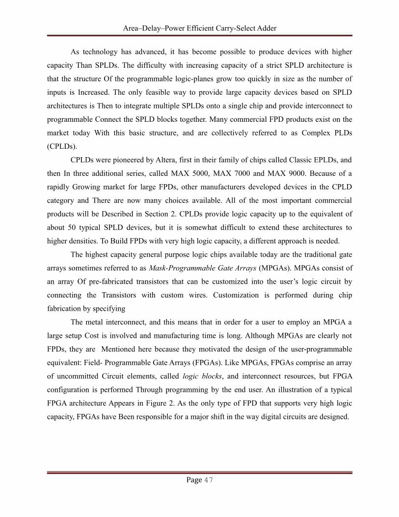
Area–Delay–Power Efficient Carry-Select Adder
As technology has advanced, it has become possible to produce devices with higher
capacity Than SPLDs. The difficulty with increasing capacity of a strict SPLD architecture is
that the structure Of the programmable logic-planes grow too quickly in size as the number of
inputs is Increased. The only feasible way to provide large capacity devices based on SPLD
architectures is Then to integrate multiple SPLDs onto a single chip and provide interconnect to
programmable Connect the SPLD blocks together. Many commercial FPD products exist on the
market today With this basic structure, and are collectively referred to as Complex PLDs
(CPLDs).
CPLDs were pioneered by Altera, first in their family of chips called Classic EPLDs, and
then In three additional series, called MAX 5000, MAX 7000 and MAX 9000. Because of a
rapidly Growing market for large FPDs, other manufacturers developed devices in the CPLD
category and There are now many choices available. All of the most important commercial
products will be Described in Section 2. CPLDs provide logic capacity up to the equivalent of
about 50 typical SPLD devices, but it is somewhat difficult to extend these architectures to
higher densities. To Build FPDs with very high logic capacity, a different approach is needed.
The highest capacity general purpose logic chips available today are the traditional gate
arrays sometimes referred to as Mask-Programmable Gate Arrays (MPGAs). MPGAs consist of
an array Of pre-fabricated transistors that can be customized into the user’s logic circuit by
connecting the Transistors with custom wires. Customization is performed during chip
fabrication by specifying
The metal interconnect, and this means that in order for a user to employ an MPGA a
large setup Cost is involved and manufacturing time is long. Although MPGAs are clearly not
FPDs, they are Mentioned here because they motivated the design of the user-programmable
equivalent: Field- Programmable Gate Arrays (FPGAs). Like MPGAs, FPGAs comprise an array
of uncommitted Circuit elements, called logic blocks, and interconnect resources, but FPGA
configuration is performed Through programming by the end user. An illustration of a typical
FPGA architecture Appears in Figure 2. As the only type of FPD that supports very high logic
capacity, FPGAs have Been responsible for a major shift in the way digital circuits are designed.
Page 47
Area–Delay–Power Efficient Carry-Select Adder
Figure 5.3 Structure of FPGA
Figure 3 summarizes the categories of FPDs by listing the logic capacities available in
each of The three categories. In the figure, “equivalent gates” refers loosely to “number of 2-
input NAND Gates”. The chart serves as a guide for selecting a specific device for a given
application, depending on the logic capacity needed. However, as we will discuss shortly, each
type of FPD is inherently better suited for some applications than for others. It should also be
mentioned that there Exist other special-purpose devices optimized for specific applications (e.g.
state machines, analog Gate arrays, large interconnection problems). However, since use of such
devices is limited They will not be described here. The next sub-section discusses the methods
used to implement the User-programmable switches that are the key to the user-customization of
FPDs.
5.3 Commercially Available FPGAs:
As one of the largest growing segments of the semiconductor industry, the FPGA market-
place is volatile. As such, the pool of companies involved changes rapidly and it is somewhat
difficult to Say which products will be the most significant when the industry reaches a stable
state. For this reason, and to provide a more focused discussion, we will not mention all of the
FPGA manufacturers That currently exists, but will instead focus on those companies whose
products are in widespread Use at this time. In describing each device we will list its capacity,
nominally in 2-input NAND gates as given by the vendor. Gate count is an especially contentious
issue in the FPGA Industry, and so the numbers given in this paper for all manufacturers should
Page 48
Area–Delay–Power Efficient Carry-Select Adder
not be taken too seriously. Wags have taken to calling them “dog” gates, in reference to the
traditional ratio between Human and dog years.
There are two basic categories of FPGAs on the market today:
1. SRAM-based FPGAs and
2. antifuse-based FPGAs.
In the first category, Xilinx and Altera are the leading manufacturers in Terms of number of
users, with the major competitor being AT&T. For antifuse-based products, Actel, Quicklogic
and Cypress, and Xilinx offer competing products.
5.4 Applications of FPGAs
FPGAs have gained rapid acceptance and growth over the past decade because they can be
applied to a very wide range of applications. A list of typical applications includes: random logic,
integrating multiple SPLDs, device controllers, communication encoding and filtering, small to
Medium sized systems with SRAM blocks, and many more.
Other interesting applications of FPGAs are prototyping of designs later to be
implemented in Gate arrays, and also emulation of entire large hardware systems. The former of
these applications Might be possible using only a single large FPGA (which corresponds to a
small Gate Array in Terms of capacity), and the latter would entail many FPGAs connected by
some sort of interconnect; For emulation of hardware, Quick Turn [Wolff90] (and others) has
developed products that Comprise many FPGAs and the necessary software to partition and map
circuits. Another promising area for FPGA application, which is only beginning to be developed,
is the Usage of FPGAs as custom computing machines. This involves using the programmable
parts to “Execute” software, rather than compiling the software for execution on a regular CPU.
The Reader is referred to the FPGA-Based Custom Computing Workshop (FCCM) held for the
last Four years and published by the IEEE.
It was mentioned in Section 2.2.8 that when designs are mapped into CPLDs, pieces of
the Design often map naturally to the SPLD-like blocks. However, designs mapped into an
FPGA are Broken up into logic block-sized pieces and distributed through an area of the FPGA.
Depending On the FPGA’s interconnect structure, there may be various delays associated with
the interconnections Between these logic blocks. Thus, FPGA performance often depends more
upon how CAD tools map circuits into the chip than is the case for CPLDs.
5.5 Design Implementation in FPGA ’s:
Page 49

Area–Delay–Power Efficient Carry-Select Adder
In the process for the implementation of the design a sequence of basic steps are
followed. The 32-bit conditional sum adder described in Chapter 4 is implemented here in FPGA
’s. The implementation is done using the following procedure.
Firstly the digital design of the circuit is created using either schematic design software
or a hardware description language. In this case, for the design of the 32-bit adder both the
methods have been tested. A schematic design of the 32 bit adder is implemented in a
hierarchical fashion, and the schematics are shown in Figure 5.2 in order of their hierarchy
starting with the lowest level blocks. In the approach using hardware description language,
VHDL code has been generated from the schematic circuit previously implemented using
Mentor Graphics tools. This VHDL code generated is used in the HDL editor of the Xilinx
Software to carry out the implementation.
Netlists are generated from the code and it is necessary to be sure that the library sets of
the targeted FPGA are available in the tool. The entire code is attached in the Appendix. 2. The
netlist produced by the design entry is transformed into a bit stream file which is used to
configure the FPGA. The design here is initially mapped onto the FPGA. This is followed by the
placement of the logic blocks created in the mapping process and, finally, the routing takes place.
This entire process is shown in the Xilinx tool as a design flow. The logic cell array file thus
obtained is converted into the bit stream file to configure the FPGA.. 3.
The final stage would be the configuration in which the circuit is downloaded onto the
FPGA. The chip used for the configuration is the Xilinx XC4010XLPC84. The demo board used
here is shown in the photograph inFigure 5.3. The board, in addition to the FPGA, also has the
PROM which is used to configure the FPGA. The FPGA could actively read the configuration
data from the PROM, or the configuration could be written into the FPGA.
5.6 VHDL (VHSIC HARDWARE DESCRIPTION LANGUAGE)
EVOLUTION OF HARDWARE DESCRIPTION LANGUAGES:
HDL’s are used to describe hardware for simulation, modeling, testing, design
and documentation. This HDL’s provide a convenient & compact format for
hierarchical representation of functional and wiring details of digital system. The
simulation process is used to verify the code. The simulation can be done at various
levels of the design from code simulation to the hard simulation. The synthesis tool is
Page 50

Area–Delay–Power Efficient Carry-Select Adder
used to directly generate the hardware by using design automation. Some of the
Languages available are
• Language for the Behavioral Model is the ISPS (Instruction Set Process
Specification) by G.Bell in 1971 from Carnegie Mellon University. It is the easy
and close to way the designer first thinks about the hardware behavior.
• Language for the Dataflow Model is the AHPL (A Hardware Programming
languages) from Arizone University.
• Language for the Structural Model or net list Model is the Verilog.
We use the test data for checking errors in the hardware i.e. using stimuli hardware
simulation is done..Generally, simulators are classified into oblivious and event
driven simulators.
• Oblivious simulator can simulate the each circuit component evaluated of
fixed time points.
• Event driven simulator can simulate the components that are evaluated.
Silicon compilers arc used to generate layout from netlists. Testing of hard
includes fault simulation, fault collapsing, test generation, test application,
test compaction, fault dictionaries.
5.7 LEVELS OF ABSTRACTION:
Behavioral: It is the most abstract model. It gives function of the design in software like
procedural form and pros ides no details as to how to implement. It is appropriate for fast
simulation of complex hardware unit, verification and functional simulation of design
ideas, modeling standard components and documentation. For simulation and functional
analysis Behavioral style doesn’t require details of the components. Description at this
level can be accessible to engineers as well as end users. It also serve as good
documentation media.
Dataflow: Concurrent representation of flow of control and movement of data. Concurrent
data components & carriers communicate through buses and interconnection and a control.
Hardware issues signals for the control of this communication. It is abstract to technical
Page 51
Area–Delay–Power Efficient Carry-Select Adder
oriented designer simulation requires flow of data through registers and busses therefore is
slower than the Input to output mapping of behavioral.
Structural: It is the lowest and most detailed level of description. It is simplest to synthesize
the hardware this includes concurrently active components and their interconnection. The
corresponding function of components is not evident description unless component used are
know A structural description that describes wiring of logic gates is said to be the Hardware
description at gate level.
A gate level description provides input for detailed timing specification
3.VHDL SOFTWARE AND ITS HISTORY
The requirements for the language were first generated in 1981 under the VHS1C program.
Since there is no standard hardware description language, the reprocurement, reuse and
exchange of designs with one another is a big issue. Thus, a need for a standardized
hardware description language for the design, documentation, and verification of digital
systems was generated. Initially the United States DoD and Woods Hole University of
Massachusetts’s started the initialization and then a team of three companies, IBM, Texas
Instruments, and Intermetrics, were first awarded the contract by the DoD (Department of
Defense) to develop a version of the language in summer 1983. They developed the
versions VHDL 2.0 after 6 months i.e. in December of 1983 VHDL 6.0 in December 1984
Version 7.2 of VHDL was developed and released to the public in 19S5 and it was called
as Language reference model (LRM). After the release of version 7.2 the language
standardization was handed to the IEEE under REVCOM Committee. They had
standardized the language and released the later versions of VDHL i.e. IEEE 1076 (A
VHDL LRM) and B VHDL LRM in the year 1987. Then the authority is turned to DASC
(Design Automation Standards Committee). TF.FF under DASC developed the VHDL’93
version.
VHDL (VHSIC HARDWARE DESCRIPTION LANGUAGE)
VHDL is the acronym of VHSIC (Very High Speed Integrated Circuit Hardware
DescriptionLanguage). It can he used to model a digital system. It contains elements that can he
Page 52
Area–Delay–Power Efficient Carry-Select Adder
used to describe the behavior or structure of the digital system, with the provision for specifying
its timing explicitly.
The language provides support for modeling the system hierarchically and
also supports top-do and bottom-up design methodologies. The system and its
subsystems can be described at any level of abstraction ranging from the architecture
level to the gate level. Precise simulation semantics are associated with all the language
constructs, and therefore, models written in this language can be verified using a
VHDL simulator.
The VHDL language can he regarded as an integrated amalgamation of thefollowing languages:
Sequential languages+
Concurrent language+
Net-list language+
Timing specifications+
Waveform generation language =>VHDL
Therefore the language has constructs that enable you to express the concurrent
or sequential behavior of a digital system with or without timing. It also allows you to
model the system as an interconnection of components. Test waveforms can also be
generated using the same constructs. The entire above constructs ma he combined to
pro a comprehensive description of the system in a single model. The language not
only defines the syntax hut also defines very clear simulation semantics for each
language construct.
VHDL is aiming at high level abstractions, portability, and design automation not
only is VHDL a description language but also a design methodology and environment.
Designers are building next- generation design technologies on VHDL. The emerging
field of electronic design automation will result in tools that allow developers to create
designs graphically at a high level of abstraction. Since
VHDL allows designing a circuit and later fabricated with the most advanced
technology VHDL is intended to provide a tool that can be used by the digital systems
Page 53

Area–Delay–Power Efficient Carry-Select Adder
community to distribute their designs in a standard format. Using VHDL, they are able
to talk to each other about their complex digital circuits in common languages without
difficulties of revealing technical details. It is a standard and unambiguous way of
exchanging de ice and system models so that engineers have a clear idea early in the
design process where components format separate contractors may need more work to
function together properly. It enables manufacturers to document and archive electronic
systems and components in a common format allowing various parties to understand
and participate in a system’s development.
As a standard description of digital systems, VHDL is used as input and output to
various simulation, synthesis and layout tools. The language provides the ability to
describe systems. Networks and components at a very high behavioral level as well as
very low gate level In a typical programming language such as C, each assignment
statement executes one after another in the specified order of the statements in the
source file.
REQUIREMENTS
The following areVHDL requirements
General Features: It should he usable for design documentation, high-level design, simulation,
synthesis and testing of hardware and as a driver for physical design tools. The description
from system to gate level concurrency.
Need for hierarchical specification of hardware
The language should provide access to various libraries user and system defined primitive and
descriptors reside in library system.
The language should provide software like sequential control Sequential & Procedural
capability is only for convenience and overall structure of VHDL remaining highly concurrent.
Languages should allow designer to configure the generic description include size, physical
Page 54
Area–Delay–Power Efficient Carry-Select Adder
characteristic timing,. Loading and environment conditions.
VHDL should allow integer, floating point, enumerate type as well as user defined types.
The languages should be strongly typed language and strong type checking.
Ability to define and use functions and procedures
Ability to specify timing at all levels is another requirement for VHDL language.
Constructs for specifying structural decomposition of hardware at all levels.
CAPABILITIES
The following are the major capabilities that the language provides along with the features
that differentiates it from other hard description languages. The language can he used as an exchange medium between chip vendors and CAD tool users.
Different chip vendors can provide VHDL descriptions of their components to system designers.
CAD tool users can use it to capture the behavior of the design at a high level of abstraction of
or functional simulation.
The language can also be used as a communication medium between different CAD and CAE
tools, for example, a schematic capture program may be used to generate a VHDL description
for the design, which can be used as an input to a simulation program.
The language supports hierarchy that is, a digital s can he modeled as a set of interconnected
components: each component, in turn, can be modeled as a set of interconnected
subcomponents.
The language supports flexible design methodologies: top-down, bottom-up, or mixed.
The language is not technology-specific, but is capable of supporting technology
specific features. It can also support various hardware technologies.
It supports both synchronous and as asynchronous timing models.
Various digital modeling techniques such as finite-state machine descriptions,
algorithmic descriptions, and Boolean equations can be modeled using the language.
The language is publicly available human-readable, machine-readable, and above all, it is not
proprietary.
The language supports three basic different description styles: structural. Data flow and
Page 55

Area–Delay–Power Efficient Carry-Select Adder
behavioral. A design may also be expressed in any combination of these three descriptive
styles.
It supports a wide range of abstraction levels ranging from abstract behavioral descriptions to
very precise gate-level descriptions. It does not, however support modeling at or below the
transistor level. It allows a design to be captured at a mixed level using a single coherent
language.
Arbitrarily large designs can be modeled using the language and there are no limitations
imposed by the language on the size of a design.
Test benches can he written using the same language to test other VHDL models.
The use of generics and attributes in the models facilitate back-annotation of static
information such as timing or placement information.
Generics and attributes are also useful in describing parameterized designs.
A model can not only describe the functionality of a design but can also contain information
about the design itself in terms of user-defined attributes, such as total area and speed.
Models written in this language can be verified by simulation since precise simulation
semantics are defined for each language construct.
BASIC TERMINOLOGY
VHDL is hardware description languages that can be used to model a digital
system. The digital system can be as simple as a logic gate or as complex as a complete
electronic system A hardware abstraction of this digital system is called an entity.
To describe an entity VHDL provides five different types of primary
constructs, called design units. They are:
1. Entity declaration
2. Architecture body
3. Configuration declaration
4. Package declaration
5. Package body
Page 56
Area–Delay–Power Efficient Carry-Select Adder
ENTITY DECLARATION:
The entity declaration specifies the name of the entity being modeled and lists the
set of interface ports. Ports are signals through which the entity communicates with the
other models in its external environment. An entity is modeled using an entity
declaration and at least one architecture.
ENTITY Component name is (INPUT & OUT PUT PORTS
Physical &Other parameters)
END Component name.
ARCHITECTURE BODY:
The internal details of an entity are specified by an architecture body using any of the
following modeling styles.
1. As a set of interconnected components (to represent structure).
2. As a set of concurrent assignment statements (to represent dataflow).
3. As a set of sequential assignment statements (to represent behavior).
4. As any combination of the above three.
ARCHITECTURE identifier of Component name is
Signals and Components declarations
Begin
(Specification of the functionality of the Component in terms of its input lines and Influencedby physical and other parameters)
End identifier;
Library Clause
The library clause makes visible the logical names of design libraries that can be referenced
within a design unit. The format of a library clause is library list-of-logical-library-names;
The following example of a library clause
library TTL, CMOS;
Page 57

Area–Delay–Power Efficient Carry-Select Adder
makes the logical names, TTL and CMOS, visible in the design unit that follows. Note
that the library clause does not make design units or items present in the library visible, it makes
only the library name visible (it is like a declaration for a library name). For example, it would be
illegal to use the expression "TTL.SYNTH_PACK.MVL" within a design unit without first
declaring the library name using the "library 1TL;" clause.
The following library clause
library STD, WORK;
is implicitly declared for every design unit.
Use Clause
There are two main forms of the use clause.
use library-name. primafy-unit-name ; --Form 1.
use library-name. primafy-unit-name. Item ; --Form 2.
The first form of the use clause allows the specified primary unit name from the specified design
library to be referenced in a design description. For example,
library CMOS;
use CMOS.NOR2;
configuration...
. . . use entity NOR2( . . . );
end;
Note that entity NOR2 must be available in compiled form in the design library, CMOS,
before attempting to compile the design unit where it is used.
The second form of the use clause makes the item declared in the pri- ' mary unit visible
and the item can, therefore, be referenced within the following design unit. For example,
library ATTLIB;
use ATTLIB.SYNTH_PACK.MVL;
-- MVL is a type declared in SYNTH_PACK package.
-- The package, SYNTH_PACK, is stored in the ATTLIB design library.
entity NAND2 is
port (A, B: in MVL; ...)...
If all items within a primary unit are to be made visible, the keyword all can be used. For
example,
Page 58

Area–Delay–Power Efficient Carry-Select Adder
use ATTLIB.SYNTH_PACK.all;
makes all items declared in package SYNTH_PACK in design library ATTLIB visible.
Items external to a design unit can be accessed by other means as well. One way is to use
a selected name. An example of using a selected name is
library ATTLIB;
use ATTLIB.SYNTH_PACK;
entity NOR2 is
port (A, B: in SYNTH_PACK.MVL; ...)...
Since only the primary unit name was made visible by the use clause, the complete name
of the item, that is, SYNTH_PACK.MVL must be specified. Another example is shown next. The
type VALUE_9 is defined in package SIMPACK that has been compiled into the CMOS design
library.
library CMOS;
package P1 is
procedure LOAD (A, B: CMOS.SIMPACK.VALUE_9; ...)...
end P1;
In this case, the primary unit name was specified only at the time of usage.
So far, we talked about exporting items across design libraries. What if it is necessary to export
items from design units that are in the same library? In this case, there is no need to specify a
library clause since every design unit has the following library clause implicitly declared.
library WORK;
The predefined design library STD contains the package STANDARD. The package
STANDARD contains the declarations for the predefined types such as CHARACTER,
BOOLEAN, BIT_VECTOR, and INTEGER. The following two clauses are also implicitly
declared for every design unit:
library STD;
use STD.STANDARD.all;
Thus all items declared within the package STANDARD are available for use in every VHDL
description.
CONFIGURATION DECLARATION:
Page 59
Area–Delay–Power Efficient Carry-Select Adder
A configuration declaration is used to select one of the possibly many architecture
bodies that an entity may have and to bind components, used to represent structure in that
architecture body to entities represented by an entity-architecture pair or by a
configuration, which reside in a design library.
PACKAGES AND PACKAGE BODY
A package provides a convenient mechanism to store and share declarations that are
common across many design units. A package is represented by
1. a package declaration, and optionally,
2. a package body.
Package Declaration
A package declaration contains a set of declarations that may possibly be shared by many
design units. It defines the interface to the package, that is, it defines items that can be made
visible to other design units, for example, a function declaration. A package body, in contrast,
contains the hidden details of a package, for example, a function body.
The syntax of a package declaration is
package package-name is
package-item-declarations "> These may be:
- subprogram declarations ~ type declarations
- subtype declarations
- constant declarations
- signal declarations
- file declarations
- alias declarations
- component declarations
- attribute declarations
- attribute specifications
- disconnection specifications
- use clauses
end [ package-name ] ;
An example of a package declaration is given next.
package SYNTH_PACK is
Page 60

Area–Delay–Power Efficient Carry-Select Adder
constant LOW2HIGH: TIME := 20ns:
type ALU_OP is (ADD, SUB, MUL, DIV, EQL);
attribute PIPELINE: BOOLEAN;
type MVL is ('U', '0', '1', 'Z');
type MVL_VECTOR is array (NATURAL range <>) of MVL;
subtype MY_ALU_OP is ALU_OP range ADD to DIV;
component NAND2
port (A, B: in MVL; C: out MVL);
end component;
end SYNTH_PACK;
Items declared in a package declaration can be accessed by other design units by using
the library and use context clauses. The set of common declarations may also include function
and procedure declarations and deferred constant declarations. In this case, the behavior of the
subprograms and the values of the deferred constants are specified in a separate design unit
called the package body. Since the previous package example did not contain any subprogram
declarations and deferred constant declarations, a package body was not necessary.
Consider the following package declaration.
use WORK.SYNTH_PACK.all:
package PROGRAM_PACK is
constant PROP_DELAY: TIME; -A deferred constant.
function "and" (L, R: MVL) return MVL;
procedure LOAD (signal ARRAY_NAME: inout MVL_VECTOR;
START_BIT, STOP_BIT, INT_VALUE: in INTEGER);
end PROGRAM_PACK;
In this case, a package body is required.
Package Body
A package body primarily contains the behavior of the subprograms and the values of the
deferred constants declared in a package declaration. It may contain other declarations as well, as
shown by the following syntax of a package body.
package body package-name is
package-body-item-daclarations "> These are:
Page 61

Area–Delay–Power Efficient Carry-Select Adder
- subprogram bodies -- complete constant declarations
- subprogram declarations
- type and subtype declarations
- file and alias declarations
- use clauses
end [ package-name ];
The package name must be the same as the name of its corresponding package
declaration. A package body is not necessary if its associated package declaration does not have
any subprogram or deferred constant declarations. The associated package body for the package
declaration, PROGRAM_PACK, described in the previous section is
package body PROGRAM_PACK is
constant PROP_DELAY: TIME := 15ns;
function "and" (L, R: MVL) return MVL is
begin
return TABLE_AND(L, R);
-- TABLE_AND is a 2-D constant defined elsewhere.
end "and";
procedure LOAD (signal ARRAY_NAME: inout MVL_VECTOR;
START_BIT, STOP_BIT, INT_VALUE: in INTEGER) is
-- Local declarations here.
begin
-- Procedure behavior here.
end LOAD;
end PROGRAM_PACK;
An item declared inside a package body has its scope restricted to be within the package
body and it cannot be made visible in other design units. This is in contrast to items declared in a
package declaration that can be accessed by other design units. Therefore, a package body is
used to store private declarations that should not be visible, while a package declaration is used
to store public declarations which other design units can access. This is very similar to
declarations within an architecture body which are not visible outside of its scope while items
declared in an entity declaration can be made visible to other design units. An important
Page 62

Area–Delay–Power Efficient Carry-Select Adder
difference between a package declaration and an entity declaration is that an entity can have
multiple architecture bodies with different names, while a package declaration can have exactly
one package body, the names for both being the same.
A subprogram written in any other language can be made accessible to design units by
specifying a subprogram declaration in a package declaration without a subprogram body in the
corresponding package body. The association of this subprogram with its declaration in the
package is not defined by the language and is, therefore, tool implementation-specific.
Design Libraries
A compiled VHDL description is stored in a design library. A design library is an area of
storage in the file system of the host environment. The format of this storage is not defined by
the language. Typically, a design library is implemented on a host system as a file directory and
the compiled descriptions are stored as files in this directory. The management of the design
libraries is also not defined by the language and is again tool implementation-specific.
An arbitrary number of design libraries may be specified. Each design library has a logical name
with which it is referenced inside a VHDL description. The association of the logical names with
their physical storage names is maintained by the host environment. There is one design library
with the logical name, STD, predefined in the language; this library contains the compiled
descriptions for the two predefined packages, STANDARD and TEXTIO. Exactly one design
library must be designated as the working library with the logical name, WORK. When a VHDL
description is compiled, the compiled description is always stored in the working library.
Therefore, before compilation begins, the logical name WORK must point to one of the design
libraries. The VHDL source is present in an ASCII file called the design file. This is processed by
the VHDL analyzer, which after verifying the syntactic and semantic correctness of the source,
compiles it into an intermediate form. The intermediate form is stored in the design library that
has been designated as the working library.
Design File
The design file is an ASCII file containing the VHDL source. It can contain one or more design
units, where a design unit is one of the following:
• entity declaration,
• architecture body,
• configuration declaration,
Page 63

Area–Delay–Power Efficient Carry-Select Adder
• package declaration,
• package body.
This means that each design unit can also be compiled separately.
A design library consists of a number of compiled design units. Design units are further
classified as
1. Primary units: These units allow items to be exported out of the design unit. They are
a. entity declaration: The items declared in an entity declaration are implicitly visible
within the associated architecture bodies.
b. package declaration: Items declared within a package declaration can be exported to
other design units using context clauses.
c. configuration declaration.
2. Secondary units: These units do not allow items declared within them to be exported out of the
design unit, that is, these items cannot be referenced in other design units. These are
a. architecture l)ody: A signal declared in an architecture body, for example, cannot be
referenced in other design units.
b. package body.
There can be exactly one primary unit with a given name in a single design library.
Secondary units associated with different primary units can have identical names in the same
design library; also a secondary unit may have the same name as its associated primary unit. For
example, assume there exists an entity called AND_GATE in a design library. It may have an
architecture body with the same name, and another entity, MY_GATE, in the same design library
may have an architecture body that also has the name, AND_GATE.
Secondary units must coexist with their associated primary units in the same design
library, for example, an entity declaration and all of its architecture bodies must reside in the
same library. Similarly, a package declaration and its associated package body must reside in a
single library. Even though a configuration declaration is a primary unit, it must reside in the
same library as the entity declaration to which it is associated.
IDENTIFIERS:
There are two kinds of identifiers in VHDL. basic identifier and extended
identifier. A basic identifier in VHDL composed of a sequence of one or more characters.
Page 64

Area–Delay–Power Efficient Carry-Select Adder
The first character in basic identifier must be a letter and last character may not be an
underscore. Lower case and upper case letters are considered to be identical when used
in basic identifier; as an example, Count, COUNT and all refer to be the same basic
identifier.
Extended identifier is a .sequence of characters written between two backlashes.
Any of allowable character can be used, including characters like. !., @ etc.. Within the
extended identifier lower and upper case letters are considered to be distinct.
DATA OBJECTS:
A data object holds the value of a specified type. It is created by means of an object’’
declaration. An example is:
Variable COUNT: INTEGER;
These resultants in creation of a data object called COUNT, which can hold integer values, the
object COUINT is also declared to be of variable class. Every data object belongs to one of the
following four classes.
1) Constants:
An object of constant class can hold a single value of a given type. This value is
assigned to the constant before simulation starts, and value cannot he changed during the
course of the simulation. For a constant declared in subprogram, the value assigned to the
constant every time the subprograms is called.
Constant declaration:
Example of constant declaration is
Constant rise_ time: Time: 10ns
It declares the object rise time, which can hold a value of type ‘time’, and value
assigned to the object at the start of simulation is 10ns.
2) Variables:
An object of variable class can also hold a single value of a given type. But different
Page 65

Area–Delay–Power Efficient Carry-Select Adder
values can he assigned to the variable at different times using a variable assignment
statement. Variable declaration:
Example of variable declaration is:
Variable CTRL_STATUS :BIT_ VECTOR (10 downto 0);
It specifies a variable object CTRL_ STATUS as an array of 11 elements. With each array
element of type BIT.
3) Signal:
An object belonging to the signal class holds a list of values, which includes the current
value of the signal and a set of possible future values that are appeared on the signal. Future
values can assign to the’ signal assignment statement. ’
Signal declaration:
Example of signal declaration:
Signal CLOCK: BIT;
The interpretation of these signal declarations is similar to that of variable
declarations. It declares the signal objects CLOCK of type BIT and gives an initial value of
‘O’.
4) File:
An object belonging to the file class contains a sequence of values. Values can he reador written to the file using read procedures and rite procedures File declaration:
A file is declared using a file declaration .The syntax of the file declaration is:
File file-name: file -type-name [open model is string expressions]
The string expression is interpreted by the host environment as the physical name of the file.
The mode specifies whether the file is to he used as a read only or write-only, or in the
appended mode.
DATA TYPES:
Every data object in VHDL can hold a value that belongs to a set of values. Using
Page 66
Area–Delay–Power Efficient Carry-Select Adder
a type declaration specifies this set of values. A type is a name that has associated with it a
set of values and set of operations.
The language also provides the facility to define new types by using type declarations
and also to define a set of operations on these types by writing functions that returns values of
this new type. All the possible types that can exist in the language can be categorized into the
following four major categories:
1) Scalar type:
Value belonging to this type appears in sequential order.
2) Composite types:
3) Access types:
4) File type:
These provide access to objects that contain a sequence of values of a given type.
OPERATORS
The predefined operators in the language are classified into the following six categories:
1) Logical operators
1 2) Relational operators
2 3) Shift operators
3 4) Adding operators
4 5) Multiplying operators
5 6) Miscellaneous operators
1) Logical operators
The seven logical operators are: And or no nand or xor xnor not
These are defined for the predefined types BIT and BOOLEAN. During evaluation of
logical operators, bit value O’ and 1’ are treated as FALSE and TRUE values of BOOLEAN
type, respectively.
2) Relational operators these are:
= < <= > >= /=
Page 67

Area–Delay–Power Efficient Carry-Select Adder
The result type for all relational operators is always a predefined type BOOLEAN.
3) Shift operators
These are:
SRL, SRR, SLA, SRA, ROL, ROR
Each of the operators takes an array an array of BIT or BOOLEAN as the tell operand
and an integer value as the right operand and performs and specified operation. If the integer
value is negative number, the opposite action is performed, that is a left shift or rotate
becomes a right shift or rotate, respectively and vice versa.
4) Adding operators these are:
+ - &
The operation for the - and operators must he of same type, with the result being of same
numeric type. The operands for the & operators can be either a one dimensional array type or an
element type.
5) Multiplying operators
These are: .
* / mod rem
The operation for the mod and rem operators on operands of’ integer type . with the result
being of same numeric type.
6) Miscellaneous operators
Page 68

Area–Delay–Power Efficient Carry-Select Adder
The miscellaneous operators are: Abs **
The abs operator is defined for any numeric type. The ** operator is defined the operand
to be of integer or floating point type and for the right operand to the of integer type only.
BEHAVIORAL MODELING
In this modeling style, the behavior of the entity is expressed using sequentially executed,
procedural type code, that is very similar in syntax and. semantics to that of a high-level
programming language like C or Pascal. A process statement is the primary mechanism used to
model the procedural type behavior of an entity. This chapter describes the process statement and
the various kinds of sequential statements that can be used within a process statement to model
such behavior.
Irrespective of the modeling style used, every entity is represented using an entity
declaration and at least one architecture body. The first two sections describe these in detail.
Entity Declaration
An entity declaration describes the external interface of the entity, that is, it gives the black-box
view. It specifies the name of the entity, the names of interface ports, their mode (i.e., direction),
and the type of ports. The syntax for an entity declaration is
entity entity-name is
[ generic ( list-of-generics-and-their-types ) ; ]
[ port ( list-of-interface-port-names-and-their-types) ; ]
[ entity-item-declarations ]
[ begin
Page 69

Area–Delay–Power Efficient Carry-Select Adder
entity-statements ]
end [ entity-name ];
The entity-name is the name of the entity and the interface ports are the signals through which
the entity passes information to and from its external environment. Each interface port can have
one of the following modes:
1. in: the value of an input port can only be read within the entity model.
2. out: the value of an output port can only be updated within the entity model; it cannot be read.
3. inout: the value of a bidirectional port can be read and updated within the entity model.
4. buffer: the value of a buffer port can be read and updated within the entity model. However, it
differs from the inout mode in that it cannot have more than one source and that the only kind of
signal that can be connected to it can be another buffer port or a signal with at most one source.
Declarations that are placed in the entity-item-declarations section are common to all the
design units that are associated with that entity declaration (these may be architecture bodies and
configuration declarations).
entity AOI is
port (A, B, C, D: in BIT; Z: out BIT);
end AOI;
The entity declaration specifies that the name of the entity is AOI and that it has four input
signals of type BIT and one output signal of type BIT. Note that it does not specify the
composition or functionality of the entity.
Architecture Body
An architecture body describes the internal view of an entity. It describes the functionality or the
structure of the entity. The syntax of an architecture body is
architecture architecture-name of entity-name is
[ architecture-item-declarations ]
begin
concurrent-statements; these are —>
process-statement
block-statement
concurrent-procedure-call
concurrent-assertion-statement
Page 70

Area–Delay–Power Efficient Carry-Select Adder
concurrent-signal-assignment-statement
component-instantiation-statement
generate-statement
end [ architecture-name ] ;
The concurrent statements describe the internal composition of the entity. All concurrent
statements execute in parallel, and therefore, their textual order of appearance within the
architecture body has no impact on the implied behavior. The internal composition of an entity
can be expressed in terms of structure, dataflow and sequential behavior. These are described
using concurrent statements. For example, component instantiations are used to express
structure, concurrent signal assignment statements are used to express dataflow and process
statements are used to express sequential behavior. Each concurrent statement is a different
element operating in parallel in a similar sense that individual gates of a design are operating in
parallel. The item declarations declare items that are available for use within the architecture
body. The names of items declared in the entity declaration, including ports and generics, are
available for use within the architecture body
due to the association of the entity name with the architecture body by the statement
architecture architecture-name of entity-name is . . .
An entity can have many internal views, each of which is described using a separate architecture
body. In general, an entity is represented using one entity declaration (that provides the external
view) and one or more architecture bodies (that provide die internal view). Here are two
examples of architecture bodies for the same AOI entity.
architecture AOI_CONCURRENT of AOI is
begin
Z <= not ( (A and B) or (C and D) );
end AOI_CONCURRENT;
architecture AOI_SEQUENTIAL of AOI is
begin
process (A, B, C, D)
variable TEMPI ,TEMP2: BIT;
begin
TEMP1 := A and B; -- statement 1
Page 71

Area–Delay–Power Efficient Carry-Select Adder
\TEMP2:=C and D; --statement 2
TEMP1 := TEMP1 or TEMP2; -- statement 3
Z<= not TEMP1; --statement 4
end process;
end AOI_SEQUENTIAL;
The first architecture body, AOI_CONCURRENT, describes the AOI entity using the dataflow
style of modeling; the second architecture body, AOI_SEQUENTIAL, uses the behavioral style
of modeling. In this chapter, we are concerned with describing an entity using the behavioral
modeling style. A process statement, which is a concurrent statement, is the primary mechanism
used to describe the functionality of an entity in this modeling style.
Process Statement
A process statement contains sequential statements that describe the functionality of a portion of
an entity in sequential terms. The syntax of a process statement is
[ process-label: ] process [ ( sensitivity-list ) ]
[process-item-declarations]
begin
sequential-statements; these are ->
variable-assignment-statement
signal-assignment-statement
wait-statement
if-statement
case-statement
loop-statement
null-statement
exit-statement
next-statement
assertion-statement
procedure-call-statement
return-statement.
end process [ process-label];
Page 72
Area–Delay–Power Efficient Carry-Select Adder
A set of signals that the process is sensitive to is defined by the sensitivity list. In other
words, each time an event occurs on any of the signals in the sensitivity list, the sequential
statements within the process are executed in a sequential order, that is, in the order in which
they appear (similar to statements in a high-level programming language like C or Pascal). The
process then suspends after executing the last sequential statement and waits for another event to
occur on a signal in the sensitivity list. Items declared in the item declarations part are available
for use only within the process.
The architecture body, AOI_SEQUENTIAL, presented earlier, contains one process
statement. This process statement has four signals in its sensitivity list and has one variable
declaration. If an event occurs on any of the signals, A, B, C, or D, the process is executed. This
is accomplished by executing statement I first, then statement 2, followed by statement 3, and
then statement 4. After this, the process suspends (simulation does not stop, however) and waits
for another event to occur on a signal in the sensitivity list
Variable Assignment Statement
Variables can be declared and used inside a process statement. A variable is assigned a value
using the variable assignment statement that typically has the form
variable-object := expression;
The expression is evaluated when the statement is executed and the computed value is assigned
to the variable object instantaneously, that is, at the current simulation time.
Variables are created at the time of elaboration and retain their values throughout the entire
simulation run (like static variables in C high-level programming language). This is because a
process is never exited; it is either in an active state, that is, being executed, or in a suspended
state, that is, waiting for a certain event to occur. A process is first entered at the start of
simulation (actually, during the initialization phase of simulation) at which time it is executed
until it suspends because of a wait statement (wait statements are described later in this chapter)
or a sensitivity list.
Consider the following process statement.
process (A)
variable EVENTS_ON_A: INTEGER := 0;
begin
EVENTS_ON_A := EVENTS_ON_A+1;
Page 73

Area–Delay–Power Efficient Carry-Select Adder
end process;
At start of simulation, the process is executed once. The variable EVENTS_ON_A gets
initialized to 0 and then incremented by 1. After that, any time an event occurs on signal A, the
process is activated and the single variable assignment statement is executed. This causes the
variable EVENTS_ON_A to be incremented. At the end of simulation, variable EVENTS_ON_A
contains the total number of events that occurred on signal A plus one.
Here is another example of a process statement.
signal A, Z: INTEGER; . . .
PZ: process (A) --PZ is a label for the process.
variable V1, V2: INTEGER;
begin
V1 := A - V2; --statement 1
Z <= - V1; --statement 2
V2 := Z+V1 * 2; -- statement 3
end process PZ;
If an event occurred on signal A at time T1 and variable V2 was assigned a value, say 10,
in statement 3, then when the next time an event occurs on signal A, say at time T2, the value of
V2 used in statement 1 would still be 10.
DATA FLOW MODELING
A dataflow model specifies the functionality of the entity without explicitly specifying its
structure. This functionality shows the flow of information through the entity, which is expressed
primarily using concurrent signal assignment statements and block statements. This is in contrast
to the behavioral style of modeling, in which the functionality of the entity is expressed using
procedural type statements that are executed sequentially. .
Concurrent Signal Assignment Statement
One of the primary mechanisms for modeling the dataflow behavior of an entity is by
using the concurrent signal assignment statement.
An example of a dataflow model for a 2-input or gate, shown .
entity OR2 is
port (signal A, B: in BIT; signal Z: out BIT);
end OR2;
Page 74
Area–Delay–Power Efficient Carry-Select Adder
Architecture OR2 of OR2 is
begin
Z <= A or B after 9 ns;
end OR2;
The architecture body contains a single concurrent signal assignment statement that
represents the dataflow of the or gate. The semantic interpretation of this statement is that
whenever there is an event (a change of value) on either signal A or B (A and B are signals in the
expression for Z), the expression on the right is evaluated and its value is scheduled to appear on
signal Z after a delay of 9 ns. The signals in the expression, A and B, form the "sensitivity list"
for the signal assignment statement.
There are two other points to mention about this example. First, the input and output
ports have their object class "signal" explicitly specified in the entity declaration. If it were not
so, the ports would still have been signals, since this is the default and the only object class that
is allowed for ports. The second point to note is that the architecture name and the entity name
are the same. This is not a problem since architecture bodies are considered to be secondary units
while entity declarations are primary units and the language allows secondary units to have the
same names as the primary units.
An architecture body can contain any number of concurrent signal assignment statements.
Since they are concurrent statements, the ordering of the statements is not important. Concurrent
signal assignment statements are executed whenever events occur on signals that are used in their
expressions. An example of a dataflow model for a 1-bit full-adder,
entity FULL_ADDER is
port (A, B, CIN: in BIT; SUM, COUT: out BIT);
end FULL_ADDER;
architecture FULL_ADDER of FULL_ADDER is
begin
SUM <= (A xor B) xor CIN after 15 ns;
COUT <= (A and B) or (B and CIN) or (CIN and A) after 10 ns;
end FULL_ADDER;
Two signal assignment statements are used to represent the dataflow of the FULL_ADDER
entity. Whenever an event occurs on signals A, B, or CIN, expressions of both the statements are
Page 75

Area–Delay–Power Efficient Carry-Select Adder
evaluated and the value to SUM is scheduled to appear after 15 ns while the value to COUT is
scheduled to appear after 10 ns. The after clause models the delay of the logic represented by the
expression. Contrast this with the statements that appear inside a process statement. Statements
within a process are executed sequentially while statements in an architecture body are all
concurrent statements and are order independent. A process statement is itself a concurrent
statement. What this means is that if there were any concurrent signal assignment statements and
process statements within an architecture body, the order of these statements also would not
matter.
Concurrent versus Sequential Signal Assignment
In the previous behaviour model we saw that signal assignment statements can also
appear within the body of a process statement. Such statements are called sequential signal
assignment statements, while signal assignment statements that appear outside of a process are
called concurrent signal assignment statements. Concurrent signal assignment statements are
event triggered, that is, they are executed whenever there is an event on a signal that appears in
its expression, while sequential signal assignment statements are not event triggered and are
executed in sequence in relation to the other sequential statements that appear within the process.
To further understand the difference between these two kinds of signal assignment statements,
consider the following two architecture bodies.
architecture SEQ_SIG_ASG of FRAGMENT1 is
- A, B and Z are signals.
begin
process (B)
begin -- Following are sequential signal assignment statements:
A<=B;
Z<=A;
end process;
end;
architecture CON_SIG_ASG of FRAGMENT2 is
begin -- Following are concurrent signal assignment statements:
Page 76
Area–Delay–Power Efficient Carry-Select Adder
A<=B;
Z<=A;
end;
In architecture SEQ_SIG_ASG, the two signal assignments are sequential signal
assignments. Therefore, whenever signal B has an event, say at time T, the first signal
assignment statement is executed and then the second signal assignment statement is executed,
both in zero time. However, signal A is scheduled to get its new value of B only at time T+Δ (the
delta delay is implicit), and Z is scheduled to be assigned the old value of A (not the value of B)
at time T+Δ also.
In architecture CON_SIG_ASG, the two statements are concurrent signal assignment
statements. When an event occurs on signal B, say at time T, signal A gets the value of B after
delta delay, that is, at time T+Δ. When simulation time advances to T+Δ, signal A will get its
new value and this event on A (assuming there is a change of value on signal A) will trigger the
second signal assignment statement that will cause the new value of A to be assigned to Z after
another delta delay, that is, at time T+2Δ. The delta delay model is explored in more detail in the
next section.
Aside from the previous difference, the concurrent signal assignment statement is
identical to the sequential signal assignment statement.
For every concurrent signal assignment statement, there is an equivalent process statement with
the same semantic meaning. The concurrent signal assignment statement:
CLEAR <= RESET or PRESET after 15 ns;
-- RESET and PRESET are signals.
is equivalent to the following process statement:.
process
begin
CLEAR <= RESET or PRESET after 15 ns;
wait on RESET, PRESET;
end process;
An identical signal assignment statement (this is now a sequential signal assignment)
appears in the body of the process statement along with a wait statement whose sensitivity list
comprises of signals used in the expression of the concurrent signal assignment statement
Page 77
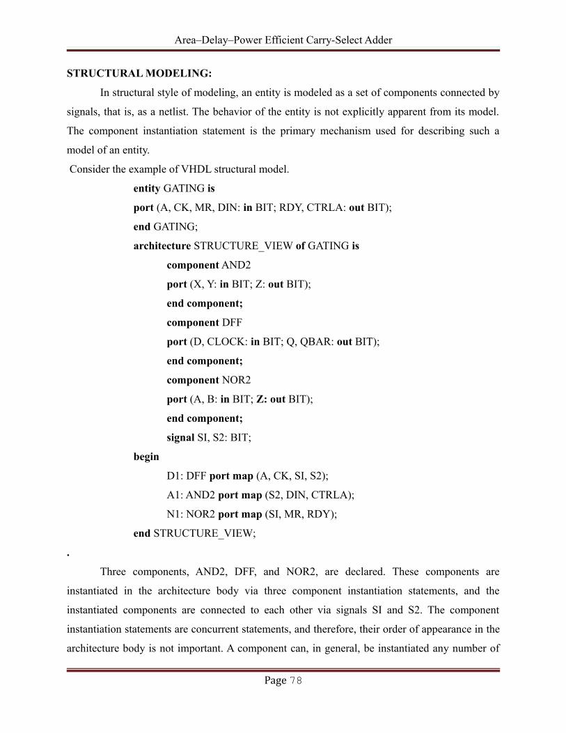
Area–Delay–Power Efficient Carry-Select Adder
STRUCTURAL MODELING:
In structural style of modeling, an entity is modeled as a set of components connected by
signals, that is, as a netlist. The behavior of the entity is not explicitly apparent from its model.
The component instantiation statement is the primary mechanism used for describing such a
model of an entity.
Consider the example of VHDL structural model.
entity GATING is
port (A, CK, MR, DIN: in BIT; RDY, CTRLA: out BIT);
end GATING;
architecture STRUCTURE_VIEW of GATING is
component AND2
port (X, Y: in BIT; Z: out BIT);
end component;
component DFF
port (D, CLOCK: in BIT; Q, QBAR: out BIT);
end component;
component NOR2
port (A, B: in BIT; Z: out BIT);
end component;
signal SI, S2: BIT;
begin
D1: DFF port map (A, CK, SI, S2);
A1: AND2 port map (S2, DIN, CTRLA);
N1: NOR2 port map (SI, MR, RDY);
end STRUCTURE_VIEW;
.
Three components, AND2, DFF, and NOR2, are declared. These components are
instantiated in the architecture body via three component instantiation statements, and the
instantiated components are connected to each other via signals SI and S2. The component
instantiation statements are concurrent statements, and therefore, their order of appearance in the
architecture body is not important. A component can, in general, be instantiated any number of
Page 78
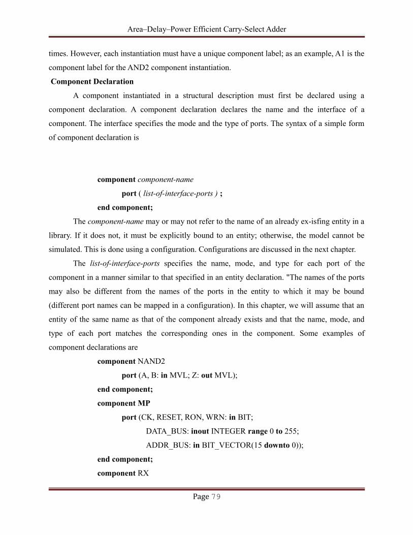
Area–Delay–Power Efficient Carry-Select Adder
times. However, each instantiation must have a unique component label; as an example, A1 is the
component label for the AND2 component instantiation.
Component Declaration
A component instantiated in a structural description must first be declared using a
component declaration. A component declaration declares the name and the interface of a
component. The interface specifies the mode and the type of ports. The syntax of a simple form
of component declaration is
component component-name
port ( list-of-interface-ports ) ;
end component;
The component-name may or may not refer to the name of an already ex-isfing entity in a
library. If it does not, it must be explicitly bound to an entity; otherwise, the model cannot be
simulated. This is done using a configuration. Configurations are discussed in the next chapter.
The list-of-interface-ports specifies the name, mode, and type for each port of the
component in a manner similar to that specified in an entity declaration. "The names of the ports
may also be different from the names of the ports in the entity to which it may be bound
(different port names can be mapped in a configuration). In this chapter, we will assume that an
entity of the same name as that of the component already exists and that the name, mode, and
type of each port matches the corresponding ones in the component. Some examples of
component declarations are
component NAND2
port (A, B: in MVL; Z: out MVL);
end component;
component MP
port (CK, RESET, RON, WRN: in BIT;
DATA_BUS: inout INTEGER range 0 to 255;
ADDR_BUS: in BIT_VECTOR(15 downto 0));
end component;
component RX
Page 79

Area–Delay–Power Efficient Carry-Select Adder
port (CK, RESET, ENABLE, DATAIN, RD: in BIT;
DATA_OUT: out INTEGER range 0 to (2**8 - 1);
PARITY_ERROR, FRAME_ERROR,
OVERRUN_ERROR: out BOOLEAN);
end component;
Component declarations appear in the declarations part of an architecture body.
Alternately, they may also appear in a package declaration. Items declared in this package
can then be made visible within any architecture body by using the library and use
context clauses. For example, consider the entity GATING described in the previous
section. A package such as the one shown next may be created to hold the component
declarations.
package COMP_LIST is
component AND2
port (X, Y: in BIT: Z: out BIT):
end component;
component DFF
port (D, CLOCK: in BIT; Q, QBAR: out BIT);
end component;
component NOR2
port (A, B: in BIT; Z: out BIT);
end component;
end COMP_LIST;
Assuming that this package has been compiled into design library DES_LIB, the
architecture body can be rewritten as
library DES_LIB;
use DES_LIB.COMP_LIST.all;
architecture STRUCTURE_VIEW of GATING is
signal S1, S2: BIT;
-- No need for specifying component declarations here, since they
-- are made visible to architecture body using the context clauses.
begin
Page 80
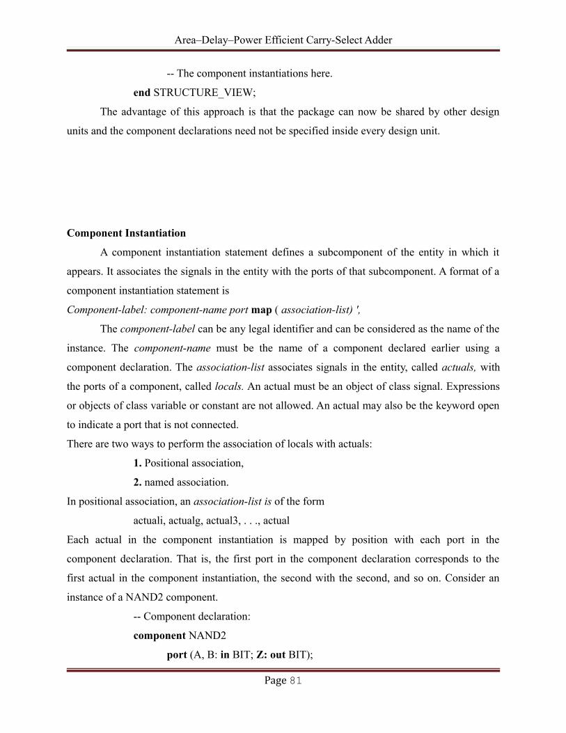
Area–Delay–Power Efficient Carry-Select Adder
-- The component instantiations here.
end STRUCTURE_VIEW;
The advantage of this approach is that the package can now be shared by other design
units and the component declarations need not be specified inside every design unit.
Component Instantiation
A component instantiation statement defines a subcomponent of the entity in which it
appears. It associates the signals in the entity with the ports of that subcomponent. A format of a
component instantiation statement is
Component-label: component-name port map ( association-list) ',
The component-label can be any legal identifier and can be considered as the name of the
instance. The component-name must be the name of a component declared earlier using a
component declaration. The association-list associates signals in the entity, called actuals, with
the ports of a component, called locals. An actual must be an object of class signal. Expressions
or objects of class variable or constant are not allowed. An actual may also be the keyword open
to indicate a port that is not connected.
There are two ways to perform the association of locals with actuals:
1. Positional association,
2. named association.
In positional association, an association-list is of the form
actuali, actualg, actual3, . . ., actual
Each actual in the component instantiation is mapped by position with each port in the
component declaration. That is, the first port in the component declaration corresponds to the
first actual in the component instantiation, the second with the second, and so on. Consider an
instance of a NAND2 component.
-- Component declaration:
component NAND2
port (A, B: in BIT; Z: out BIT);
Page 81

Area–Delay–Power Efficient Carry-Select Adder
end component;
-- Component instantiation:
N1: NAND2 port map (S1, S2, S3);
N1 is the component label for the current instantiation of the NAND2 component. Signal S1
(which is an actual) is associated with port A (which is a local) of the NAND2 component, S2 is
associated with port B of the NAND2 component, and S3 is associated with port Z. Signals S1
and S2 thus provide the two input values to the NAND2 component and signal S3 receives the
output value from the component. The ordering of the actuals is, therefore, important.
If a port in a component instantiation is not connected to any signal, the keyword open
can be used to signify that the port is not connected. For example,
N3: NAND2 port map (S1, open, S3);
The second input port of the NAND2 component is not connected to any signal. An input
port may be left open only if its declaration specifies an initial value. For the previous
component instantiation statement to be legal, a component declaration for NAND2 may appear
like
component NAND2
port (A, B: in BIT := '0'; Z: out BIT);
- Both A and B have an initial value of '0'; however, only
- the initial value of B is necessary in this case.
end component;
A port of any other mode may be left unconnected as long as it is not an unconstrained
array.
In named association, an association-list is of the form
locale => actual1, local2 => actual2, ..., localn => actualn
For example, consider the component NOR2 in the entity GATING described in the first section.
The instantiation using named association may be written as
N1: NOR2 port map (B=>MR, Z=>RDY, A=>S1);
In this case, the signal MR (an actual), that is declared in the entity port list, is associated
with the second port (port B, a local) of the NOR2 gate, signal RDY is associated with the third
port (port Z) and signal S1 is associated with the first port (port A) of the NOR2 gate. In named
association, the ordering of the associations is not important since the mapping between the
Page 82
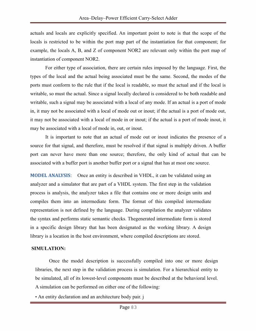
Area–Delay–Power Efficient Carry-Select Adder
actuals and locals are explicitly specified. An important point to note is that the scope of the
locals is restricted to be within the port map part of the instantiation for that component; for
example, the locals A, B, and Z of component NOR2 are relevant only within the port map of
instantiation of component NOR2.
For either type of association, there are certain rules imposed by the language. First, the
types of the local and the actual being associated must be the same. Second, the modes of the
ports must conform to the rule that if the local is readable, so must the actual and if the local is
writable, so must the actual. Since a signal locally declared is considered to be both readable and
writable, such a signal may be associated with a local of any mode. If an actual is a port of mode
in, it may not be associated with a local of mode out or inout; if the actual is a port of mode out,
it may not be associated with a local of mode in or inout; if the actual is a port of mode inout, it
may be associated with a local of mode in, out, or inout.
It is important to note that an actual of mode out or inout indicates the presence of a
source for that signal, and therefore, must be resolved if that signal is multiply driven. A buffer
port can never have more than one source; therefore, the only kind of actual that can be
associated with a buffer port is another buffer port or a signal that has at most one source.
MODEL ANALYSIS: Once an entity is described in VHDL, it can be validated using an
analyzer and a simulator that are part of a VHDL system. The first step in the validation
process is analysis, the analyzer takes a file that contains one or more design units and
compiles them into an intermediate form. The format of this compiled intermediate
representation is not defined by the language. During compilation the analyzer validates
the syntax and performs static semantic checks. Thegenerated intermediate form is stored
in a specific design library that has been designated as the working library. A design
library is a location in the host environment, where compiled descriptions are stored.
SIMULATION:
Once the model description is successfully compiled into one or more design
libraries, the next step in the validation process is simulation. For a hierarchical entity to
be simulated, all of its lowest-level components must be described at the behavioral level.
A simulation can be performed on either one of the following:
• An entity declaration and an architecture body pair. j
Page 83

Area–Delay–Power Efficient Carry-Select Adder
• A configuration
Preceding the actual simulation are two major steps:
1. ELABORATION PHASE: In this phase, the hierarchy of the entity is expanded and
linked, components are bound to entities in a library, and the top-level entity is built as a
network of behavioral models that is ready to be simulated.
2. INITIALIZATION PHASE: Driving and effective values for all explicitly declared
signals are computed, implicitly signals are assigned values, processes are executed once
until they suspended and simulation time is set to 0 ns.
Simulation commences by advancing time to that of the next event. Values that are
scheduled to be assigned to signals at this time are assigned.
DESIGN AUTOMATION:
The design phase is complete when idea is transformed to architecture or a data
path description. The remaining is a routine work and involves tasks that a machine can
do much faster than a talented engineer. Activities such as transforming one form to
another form of design & certification of each design stage and generating test data are
ref to as design automation. Modeling is an art and designer uses modeling tools for
representing an idea. Modeling tools include paper & pencil, schematic capture
programs, bread boarding felicities and hardware description Languages.
GENERAL PROCEDURE TO USE PROJECT NAVIGATOR
❖ Click on “ Project Navigator Icon”
❖ Go to File Icon on the tool bar
❖ Go to “New Project”
❖ Project Location E:/
❖ Project name xxxx.
❖ Device family - vertex 2
❖ Click on Next
Next
Next
Page 84
Area–Delay–Power Efficient Carry-Select Adder
Finish
❖ New file ( ctrl+n) my project will be seen in “ sources in project’
❖ File save as “xxxx vhd”
❖ Type the VHDL code in the space and save and save
❖ Go to project tool bar add “source”
❖ And click on the “xxxx .vhd”
❖ Observe that the “xxxx .VHD” file is added to the current project work space along
with the entity name
❖ Go to processes for source click on the “syntax”
❖ Check for errors in “error window :. If any errors correct them again check syntax up to
get check syntax ok (-/)
❖ Then click on the “Launch Model sim”
❖ Then you can get signal window, wave default window and structure window
❖ Apply appropriate signals in signals window and observe signals on wave default
window after clicking Run icon (Jfj)
GENERAL PROCEDURE FOR DUMPING VHDL PROGRAM IN TARGET DEVICE
LIKE FPGA OR CPLD:
1.Connect FPGA/CPLD to CPU through JTAG cable and give power supply through
5V adapter( In FPGA Slave Serial Mode and in CPLD Boundary Scan Mode is used)
2.Go to user constraints then
3.Assign package pins and double click on it then give pin no’s like
“p74”,’P76”,”p100’’.
4.Go to Synthesis XST then double click on it
5.Go to Implementation design then double click on it
6.Go to Configure divice (IMPACT ) then double click on it
7.Progress dialog box will appear and wait until it completes
8.Right click device on Xilinx chip diagram to dump the program
9.Now the VHDL program dumping is completed
10.Outputs are verified by varying different combinations of inputs accroding to the
truth table.
Page 85

Area–Delay–Power Efficient Carry-Select Adder
CHAPTER-6
RESULTS
FIG 7.1 Comparison of areas
Fig 7.2 comparison of delays
Figure 7.3 Power delay comparison
7.1 Experimental results:(A) RIPPLE CARRY ADDER:
Page 86

Area–Delay–Power Efficient Carry-Select Adder
Fig schematic diagram
Figure 7.4 32 bit ripple carry adder
(B) PROPOSED RESULTS
Page 87
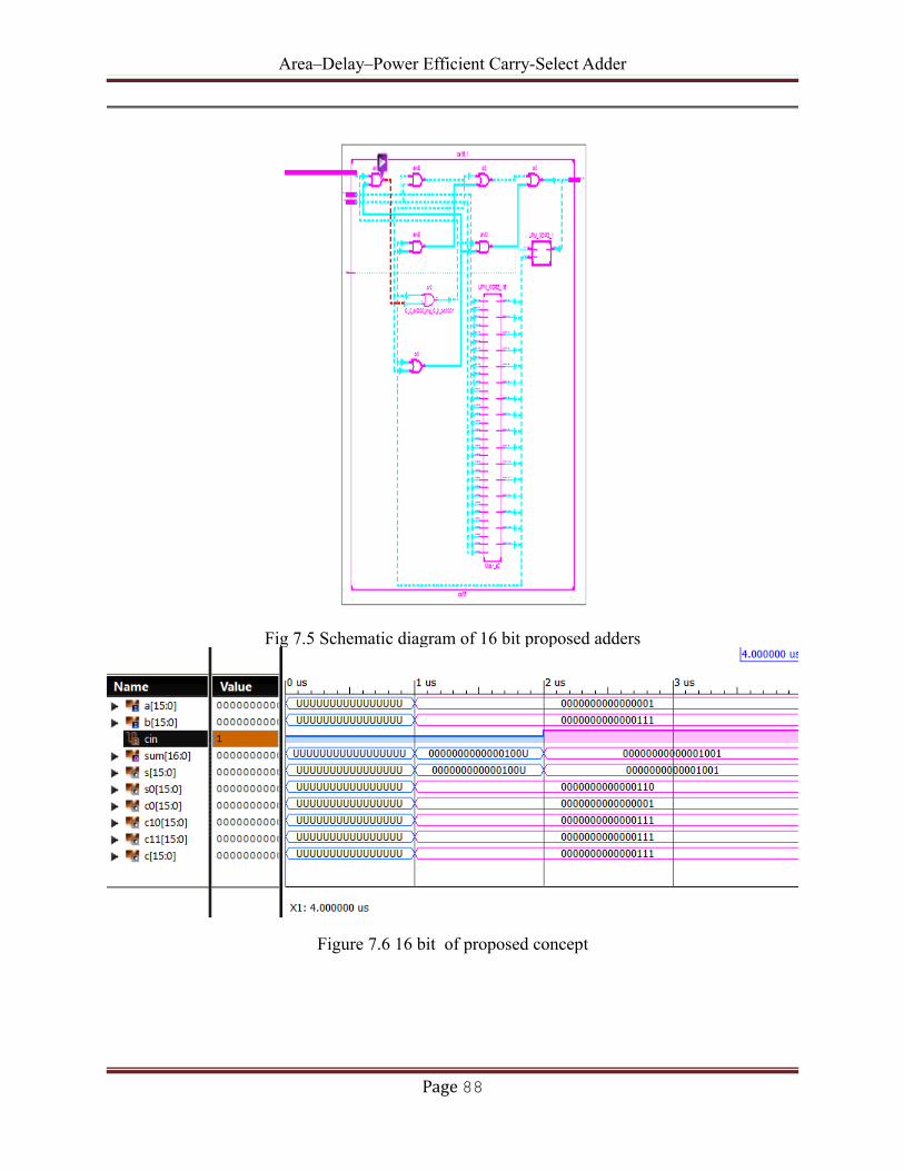
Area–Delay–Power Efficient Carry-Select Adder
Fig 7.5 Schematic diagram of 16 bit proposed adders
Figure 7.6 16 bit of proposed concept
Page 88

Area–Delay–Power Efficient Carry-Select Adder
Fig 7.7 32 bit of proposed concept
Fig 7.8 Results of 32 bit proposed adders
EXTENSION RESULTS:
Page 89

Area–Delay–Power Efficient Carry-Select Adder
Fig 7.9 Extension schematic diagram
Fig 7.10 Results of extension 16 bit
CHAPTER-7
CONCLUSION
CONCLUSION
Thus in order to reduce the area and power of SQRT CSLA architecture that we have
implemented in this Project, a simple approach has been used. In this work, the numbers of gates
Page 90

Area–Delay–Power Efficient Carry-Select Adder
have been reduced and this feature offers a greater advantage in the area and power reduction.
The simulation results indicate that the modified SQRT CSLA is suffering from larger delay
whereas the in 32-bit modified SQRT CSLA, area and power are significantly reduced. The
delay calculations used here can be computed using the mentor graphics tool.
FUTURE SCOPE
Now a day’s Carry Select Adder (CSLA) used in many data-processing processors to perform
fast arithmetic functions. The speed of SQRT CSLA greater than Modified SQRT CSLA, but the
area and power reduced compared to SQRT CSLA. So, SQRT CSLA can be replaced by
Modified SQRT CSLA Where the area and power major constraints than speed.
REFERENCES
[1] K. K. Parhi, VLSI Digital Signal Processing. New York, NY, USA: Wiley, 1998.
[2] A. P. Chandrakasan, N. Verma, and D. C. Daly, “Ultralow-power electron ics for biomedical
applications,” Annu. Rev. Biomed. Eng., vol. 10, pp. 247– 274, Aug. 2008.
[3] O. J. Bedrij, “Carry-select adder,” IRE Trans. Electron. Comput., vol. EC-11, no. 3, pp. 340–
344, Jun. 1962.
[4] Y. Kim and L.-S. Kim, “64-bit carry-select adder with reduced area,” Electron. Lett., vol. 37,
no. 10, pp. 614–615, May 2001.
[5] Y. He, C. H. Chang, and J. Gu, “An area-efficient 64-bit square root carry select adder for low
power application,” in Proc. IEEE Int. Symp. Circuits Syst., 2005, vol. 4, pp. 4082–4085.
[6] B. Ramkumar and H. M. Kittur, “Low-power and area-efficient carry-select adder,” IEEE
Trans. Very Large Scale Integr. (VLSI) Syst., vol. 20, no. 2,
Page 91

Area–Delay–Power Efficient Carry-Select Adder
pp. 371–375, Feb. 2012.
[7] I.-C. Wey, C.-C. Ho, Y.-S. Lin, and C. C. Peng, “An area-efficient carry select adder design
by sharing the common Boolean logic term,” in Proc. IMECS, 2012, pp. 1–4.
[8] S. Manju and V. Sornagopal, “An efficient SQRT architecture of carry select adder design by
common Boolean logic,” in Proc. VLSI ICEVENT, 2013, pp. 1–5.
[9] B. Parhami, Computer Arithmetic: Algorithms and Hardware Designs, 2nd ed. New York,
NY, USA: Oxford Univ. Press, 2010.
Page 92